Embed Size (px)
Citation preview
Plasma Sourcesfor EUV Lithography
David Attwood
University of California, Berkeley
(http://www.coe.berkeley.edu/AST/sxr2009)
Lecture 18 / EUV Plasma Sources / Spring 2009
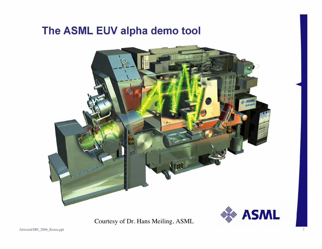
SPIE 2004 Santa Clara, CA / Intro to EUV Lithography 2Attwood/SRI_2006_Korea.ppt
Courtesy of Dr. Hans Meiling, ASML
CU_Jan12_04.pptD. Attwood 10
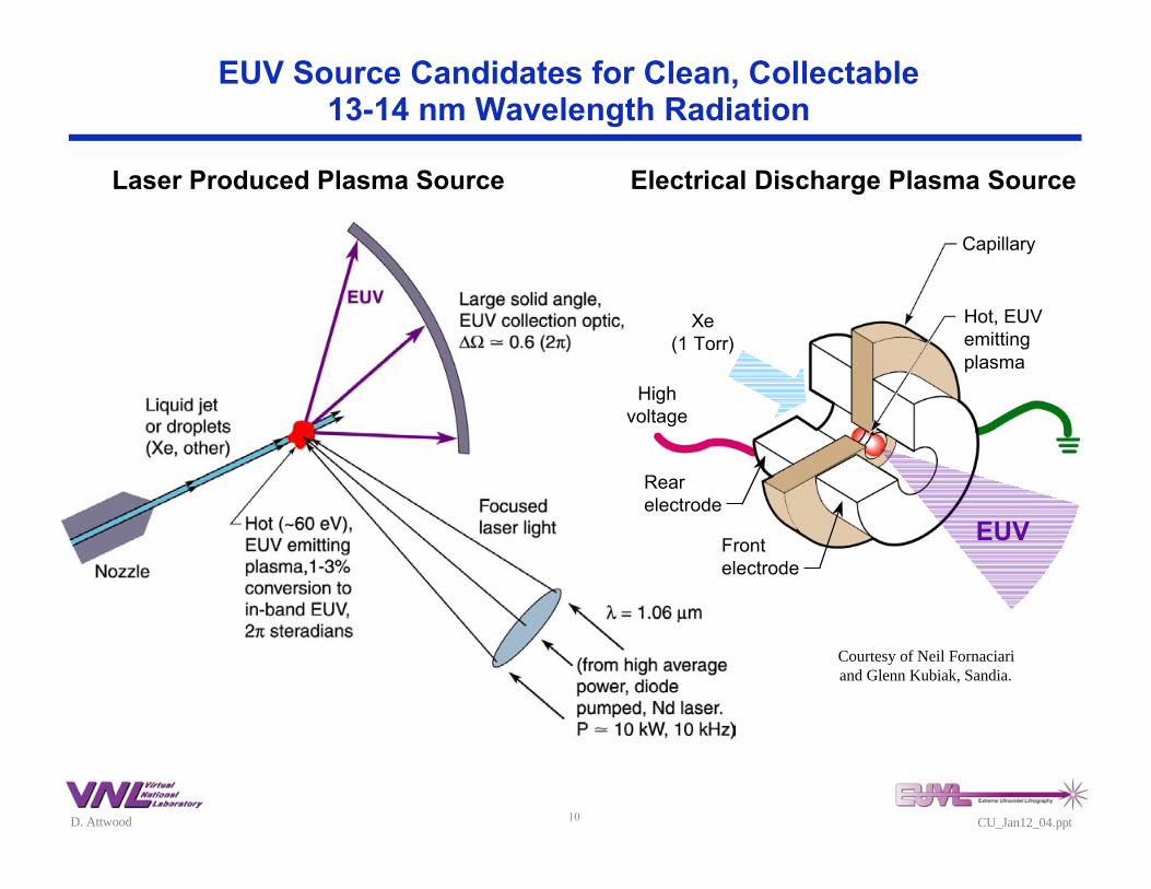
EUV Source Candidates for Clean, Collectable13-14 nm Wavelength Radiation
Laser Produced Plasma Source Electrical Discharge Plasma Source
Courtesy of Neil Fornaciariand Glenn Kubiak, Sandia.
EUV
Rearelectrode
Frontelectrode
Capillary
Hot, EUVemittingplasma
Xe(1 Torr)
Highvoltage
J. Phys. D: Appl. Phys. (London) 37, 3207(2004)
Ch10_thruputModls_June08.ai
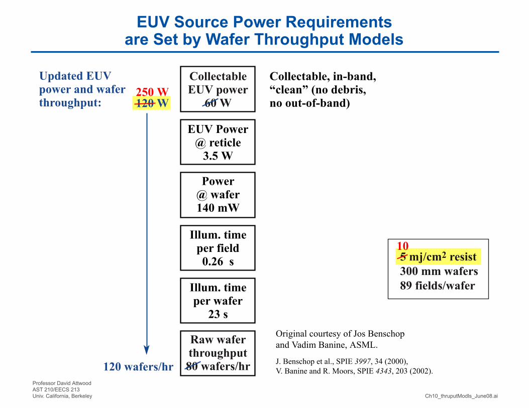
EUV Source Power Requirementsare Set by Wafer Throughput Models
Professor David AttwoodAST 210/EECS 213Univ. California, Berkeley
Original courtesy of Jos Benschopand Vadim Banine, ASML.
J. Benschop et al., SPIE 3997, 34 (2000),V. Banine and R. Moors, SPIE 4343, 203 (2002).
CollectableEUV power
60 W
Updated EUVpower and waferthroughput:
5 mj/cm2 resist300 mm wafers89 fields/wafer
Collectable, in-band,“clean” (no debris,no out-of-band)
EUV Power@ reticle
3.5 W
Power@ wafer140 mW
Illum. timeper field0.26 s
Illum. timeper wafer
23 s
Raw waferthroughput80 wafers/hr
120 W250 W
10
120 wafers/hr
Jason Dimkoff AST 213
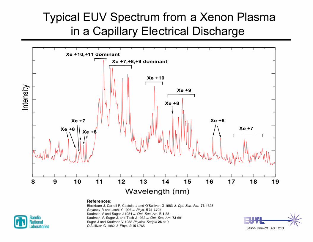
Typical EUV Spectrum from a Xenon Plasmain a Capillary Electrical Discharge
8 9 10 11 12 13 14 15 16 17 18 19
Xe +7,+8,+9 dominant
Xe +8
Xe +10,+11 dominant
Xe +10
Xe +7
Xe +8
Xe +8
Xe +8
Xe +7
Xe +9
Inte
nsity
Wavelength (nm)
References:Blackburn J, Carroll P, Costello J and O’Sullivan G 1983 J. Opt. Soc. Am. 73 1325Gayasov R and Joshi Y 1998 J. Phys. B 31 L705Kaufman V and Sugar J 1984 J. Opt. Soc. Am. B 1 38Kaufman V, Sugar J, and Tech J 1983 J. Opt. Soc. Am. 73 691Sugar J and Kaufman V 1982 Physica Scripta 26 419O’Sullivan G 1982 J. Phys. B 15 L765
VirtualNational
Laboratory
Jason Dimkoff SNL EUVL
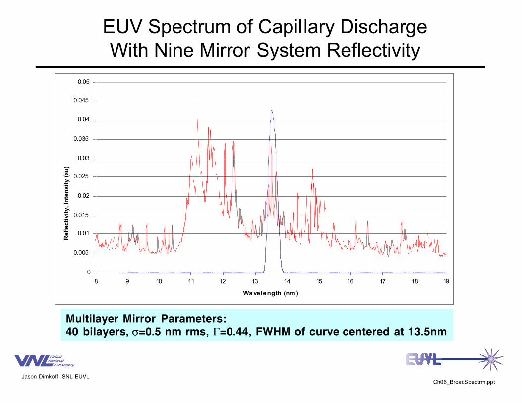
EUV Spectrum of Capillary DischargeWith Nine Mirror System Reflectivity
Multilayer Mirror Parameters:40 bilayers, σ=0.5 nm rms, Γ=0.44, FWHM of curve centered at 13.5nm
0
0.005
0.01
0.015
0.02
0.025
0.03
0.035
0.04
0.045
0.05
8 9 10 11 12 13 14 15 16 17 18 19
Wa velength (nm )
Re
fle
cti
vit
y,
Inte
ns
ity
(a
u)
Ch06_BroadSpectrm.ppt
Ch06_Xe_Sn_Spectra.ai
Professor David AttwoodAST 210/EECS 213Univ. California, Berkeley
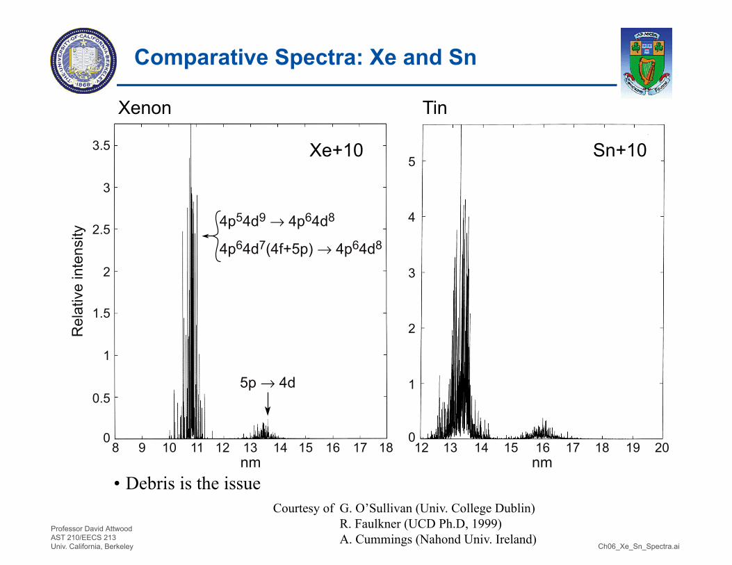
Comparative Spectra: Xe and Sn
80 0
1
2
3
4
5
0.5
1.5
1
2.5
2
3.5
3
9 10 11 12 13
4p54d9 → 4p64d8
5p → 4d
4p64d7(4f+5p) → 4p64d8
Xe+10
Xenon
• Debris is the issue
Tin
Sn+10
Rel
ativ
e in
tens
ity
14 15 16 17 18 12 13 14 15 16 1817 19 20nmnm
Courtesy of G. O’Sullivan (Univ. College Dublin) R. Faulkner (UCD Ph.D, 1999) A. Cummings (Nahond Univ. Ireland)
Laser Plasma Laboratory College of Optics & Photonics: CREOL & FPCE at UCF
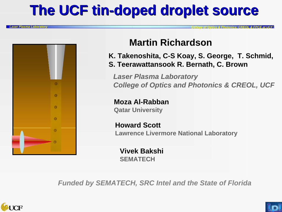
The UCF tinThe UCF tin--doped droplet sourcedoped droplet source
Martin RichardsonK. Takenoshita, C-S Koay, S. George, T. Schmid, S. Teerawattansook R. Bernath, C. Brown
Laser Plasma LaboratoryCollege of Optics and Photonics & CREOL, UCF
Moza Al-RabbanQatar University
Howard ScottLawrence Livermore National Laboratory
Vivek BakshiSEMATECH
Funded by SEMATECH, SRC Intel and the State of Florida
Laser Plasma Laboratory College of Optics & Photonics: CREOL & FPCE at UCF
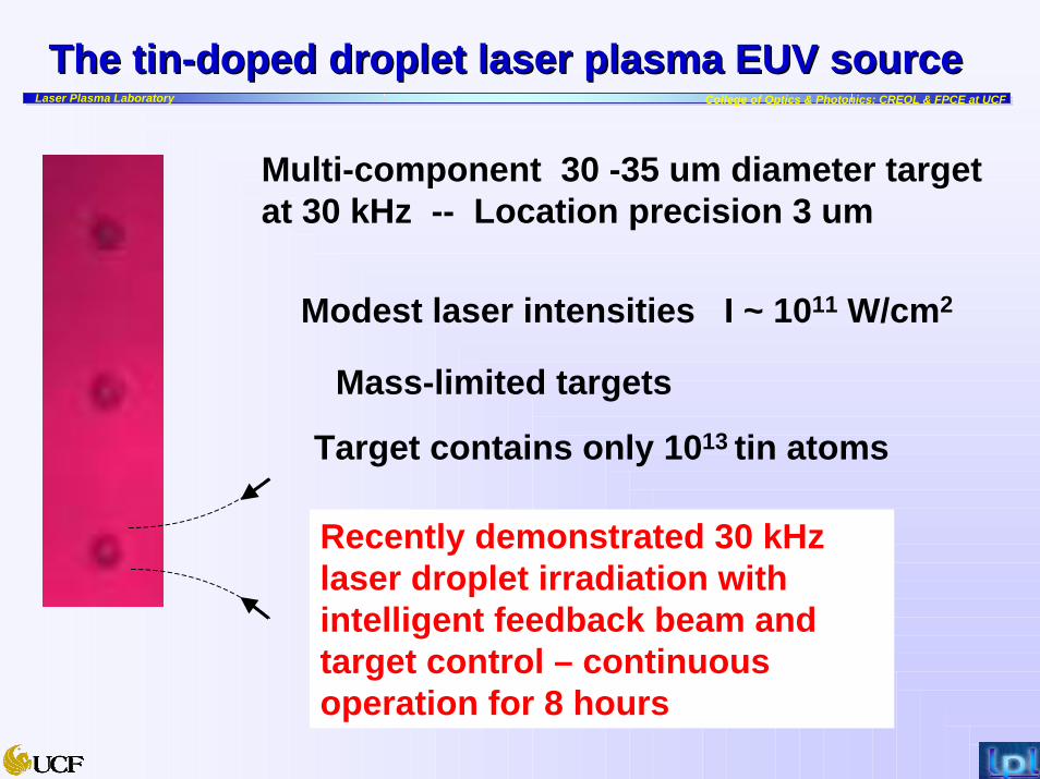
The tinThe tin--doped droplet laser plasma EUV sourcedoped droplet laser plasma EUV source
Multi-component 30 -35 um diameter target at 30 kHz -- Location precision 3 um
Modest laser intensities I ~ 1011 W/cm2
Mass-limited targets
Target contains only 1013 tin atoms
Recently demonstrated 30 kHz laser droplet irradiation with intelligent feedback beam and target control – continuous operation for 8 hours
Laser Plasma Laboratory College of Optics & Photonics: CREOL & FPCE at UCF
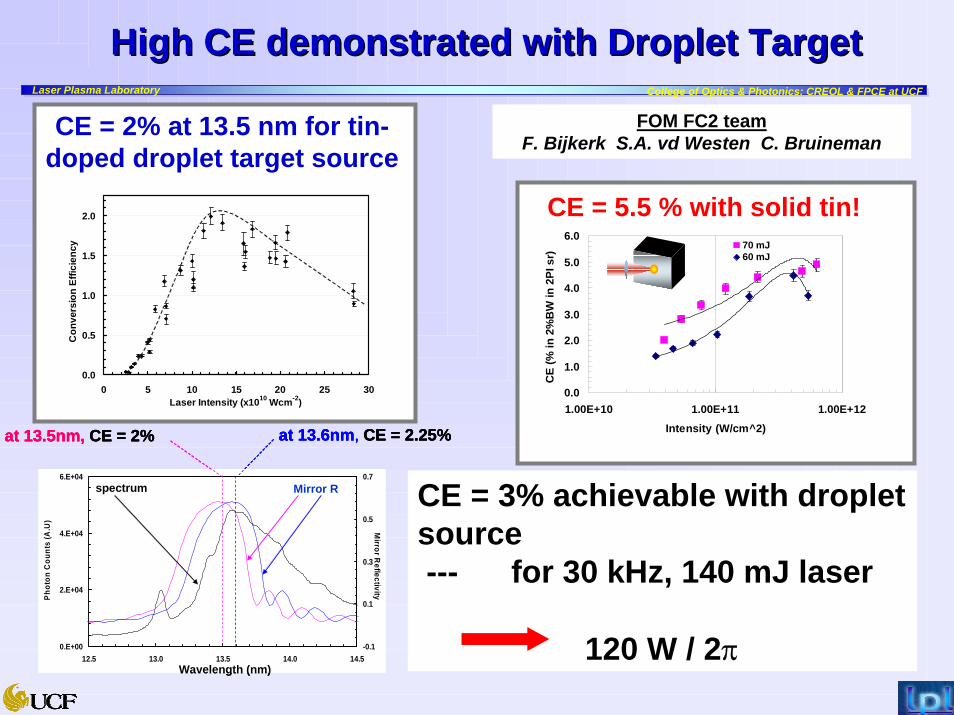
High CE demonstrated with Droplet TargetHigh CE demonstrated with Droplet Target
CE = 2% at 13.5 nm for tin-doped droplet target source
0.0
0.5
1.0
1.5
2.0
0 5 10 15 20 25 30
Co
nv
ers
ion
Eff
icie
ncy
Laser Intensity (x1010 Wcm-2)
0.0
0.5
1.0
1.5
2.0
0 5 10 15 20 25 30
Co
nv
ers
ion
Eff
icie
ncy
Laser Intensity (x1010 Wcm-2)
0.E+00
2.E+04
4.E+04
6.E+04
12.5 13.0 13.5 14.0 14.5
-0.1
0.1
0.3
0.5
0.7
Mirro
r Refle
ctivityPh
oto
n C
ou
nts
(A.U
)
spectrum Mirror R
at 13.5nm, CE = 2% at 13.6nm, CE = 2.25%
Wavelength (nm)
0.E+00
2.E+04
4.E+04
6.E+04
12.5 13.0 13.5 14.0 14.5
-0.1
0.1
0.3
0.5
0.7
Mirro
r Refle
ctivityPh
oto
n C
ou
nts
(A.U
)
spectrum Mirror R
at 13.5nm, CE = 2% at 13.6nm, CE = 2.25%
0.E+00
2.E+04
4.E+04
6.E+04
12.5 13.0 13.5 14.0 14.5
-0.1
0.1
0.3
0.5
0.7
Mirro
r Refle
ctivityPh
oto
n C
ou
nts
(A.U
)
spectrum Mirror R
0.E+00
2.E+04
4.E+04
6.E+04
12.5 13.0 13.5 14.0 14.5
-0.1
0.1
0.3
0.5
0.7
Mirro
r Refle
ctivityPh
oto
n C
ou
nts
(A.U
)
spectrum Mirror R
0.E+00
2.E+04
4.E+04
6.E+04
12.5 13.0 13.5 14.0 14.5
-0.1
0.1
0.3
0.5
0.7
Mirro
r Refle
ctivityPh
oto
n C
ou
nts
(A.U
)
spectrum Mirror R
at 13.5nm, CE = 2% at 13.6nm, CE = 2.25%
Wavelength (nm)
0.0
1.0
2.0
3.0
4.0
5.0
6.0
1.00E+10 1.00E+11 1.00E+12
Intensity (W/cm^2)
CE
(%
in 2
%B
W in
2P
I sr)
70 mJ60 mJ
CE = 5.5 % with solid tin!
CE = 3% achievable with droplet source--- for 30 kHz, 140 mJ laser
120 W / 2π
FOM FC2 teamF. Bijkerk S.A. vd Westen C. Bruineman
yrotarobaL amsalP resaL FCU ta ECPF & LOERC :scinotohP & scitpO fo egelloC
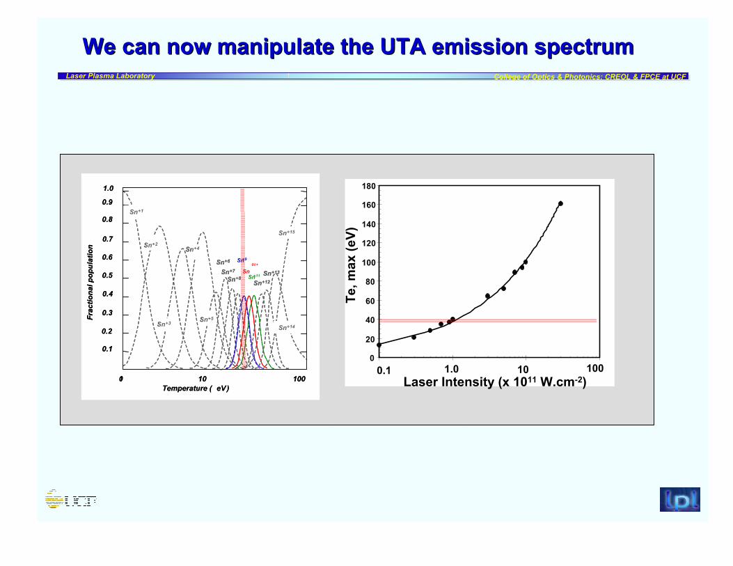
murtceps noissime ATU eht etalupinam won nac eW murtceps noissime ATU eht etalupinam won nac eWal
ized
Pho
ton
Cou
nt(A
.U.)
f::g:h
x 1.1 01 21:ix 6.8 01 11x 8.3 01 11x 4.1 01 11 /W mc 2
1x5.0 0 31
1x0.1 0 31
08 09 01 0 11 0 21 0 031 41 0 51 0 61 0Wa ev le ( htgn Å)
1x5.0 0 31
1x0.1 0 31
1x5.1 0 31
1x0.2 0 31
08 09 01 0 11 0 21 0 31 0 41 0 051 061 71 0 81 0 91 0 002Wa ev le ( htgn Å)
1x5.0 0 31
1x0.1 0 31
1x5.1 0 31
1x0.2 0 31
1x5.2 0 31
1x0.3 0 31
08 09 01 0 11 0 21 0 31 0 41 0 051 061 71 0 81 0 91 0 002
nS 9+
-bN Like t inAg ces( 1- )
aW velength ( Å)
nS 9+
0
21 .5 31 .0 13.5 14.0 14.5 51 .0 51 .5
Waveleng ht n( )m
Nor
mal
ized
Pho
ton
Co
a
b
c
d
.0 01x5 31
.1 01x0 31
.1 01x5 31
.2 01x0 31
.2 01x5 31
.3 01x0 31
08 09 001 011 021 031 041 51
nS 11+
-Y -Like t inAg (sec 1- )
Wa lev tgne h
.0 5x 01 31
.1 0x 01 31
.1 5x 01 31
.2 0x 01 31
.2 5x 01 31
.3 0x 01 31
08 09 01 0 011 21 0 31 0 041 51 0 61 0 071 81 0 91 0 002
Z L-r ki e t in( Ag s ce 1- )
Wave el ng ht Å( )
nS 1+ 0 nS 1+ 0
1x0.2 0 31
1x5.2 0 31
1x0.3 0 31
nS 9+
-bN Like t inAg ces( 1- )
nS 9+
0
02
04
06
08
001
021
041
061
1.0 0.1 01 01 00
02
04
06
08
001
021
041
061
1.0 0.1 01 01 0ytisnetnI resaL 01 x( 11 mc.W 2- )
Te, m
ax (e
V)0 01 001
eT pm re ruta e ( eV )
9.0
8.0
7.0
6.0
5.0
4.0
3.0
2.0
1.0
nS 1+
nS 2+
nS 3+
nS 4+
nS 5+
nS 6+
nS 7+
nS
nS 1+ 0
nS 8+nS 21+
nS 31+
nS 41+
nS 51+
Frac
tiona
l pop
ulat
ion
1 01 001eT pm re ruta e ( eV )
9.0
8.0
7.0
6.0
5.0
4.0
3.0
2.0
1.0
nS 1+
nS 2+
nS 3+
nS 4+
nS 5+
nS 6+
nS 7+
9+
nS
1+0
nS 1+ 1nS 8+
nS 21+nS 31+
nS 41+
nS 51+
Frac
tiona
l pop
ulat
ion
0
02
04
06
08
001
021
041
061
081
1.0 0.1 01 01 00
02
04
06
08
001
021
041
061
081
1.0 0.1 01 01 0ytisnetnI resaL 01 x( 11 mc.W 2- )
Te, m
ax (e
V)
0 01 001eT pm re ruta e ( eV )
0.1
9.0
8.0
7.0
6.0
5.0
4.0
3.0
2.0
1.0
nS 1+
nS 2+
nS 3+
nS 4+
nS 5+
nS 6+
nS 7+
nS
nS 1+ 0
nS 8+nS 21+
nS 31+
nS 41+
nS 51+
Frac
tiona
l pop
ulat
ion
1 01 001eT pm re ruta e ( eV )
0.1
9.0
8.0
7.0
6.0
5.0
4.0
3.0
2.0
1.0
nS 1+
nS 2+
nS 3+
nS 4+
nS 5+
nS 6+
nS 7+
9+
nS
1+0
nS 1+ 1nS 8+
nS 21+nS 31+
nS 41+
nS 51+
Frac
tiona
l pop
ulat
ion
Laser Plasma Laboratory College of Optics & Photonics: CREOL & FPCE at UCF
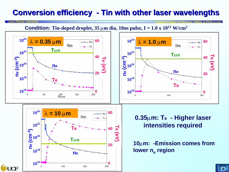
Hydrodynamic Modeling: Effects of Laser WavelengthConversion efficiency Conversion efficiency -- Tin with other laser wavelengthsTin with other laser wavelengths
Condition: Tin-doped droplet, 35 µm dia, 10ns pulse, I = 1.0 x 10¹¹ W/cm2
0.35µm: Te - Higher laser intensities required
1.0E+16
1.0E+18
1.0E+20
1.0E+22
1.0E+24
0 50 100 150 200
0
20
40
60Ne
Te
R(≅m)
0nsλ = 0.35 µm
Te
ne
Tcrit
1016
1018
1020
1022
1024
20
0
40
60
ne
(cm
-3) T
e (eV)
1.0E+16
1.0E+18
1.0E+20
1.0E+22
1.0E+24
0 100 200
0
20
40
60Ne
Te0nsλ = 1.0 µm
1016
1018
1020
1022
1024
20
0
40
60
ne
(cm
-3)
Te (eV
)
Tcrit
ne
Te
1.0E+16
1.0E+18
1.0E+20
1.0E+22
1.0E+24
0 100 200 300
0
20
40
60Ne
Te0nsλ = 10 µm
1016
1018
1020
1022
1024
ne
(cm
-3)
20
0
40
60T
e (eV)Tcrit
ne
Te
10µm: -Emission comes from lower ne region
Laser Plasma Laboratory College of Optics & Photonics: CREOL & FPCE at UCF
SummarySummary
Multi-component droplet laser plasma droplet plasma
30 kHz laser irradiated droplet system demonstrated
CE = 2.3% with a droplet – 5.5 % (solid tin) - > 3% possible
Droplet has only 1013 per target
Low energy ions only at mirror – no anomalous fast ions
Repeller Field stops both ions AND particles
Combination of mitigation schemes should provide enough mirror protection
EUVL Symposium 2008 – Lake Tahoe CA September 30, 2008
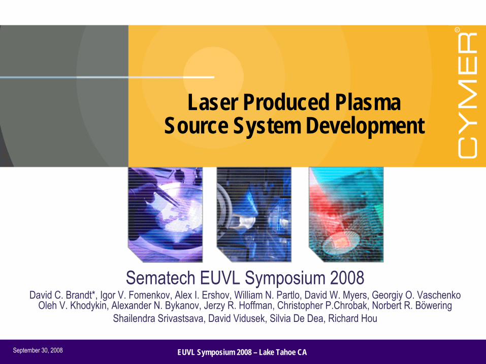
Laser Produced Plasma Source System Development
Sematech
EUVL Symposium 2008David C. Brandt*, Igor V. Fomenkov, Alex I. Ershov, William N. Partlo, David W. Myers, Georgiy
O. Vaschenko
Oleh
V. Khodykin, Alexander N. Bykanov, Jerzy
R. Hoffman, Christopher P.Chrobak, Norbert R. BöweringShailendra
Srivastsava, David Vidusek, Silvia De Dea, Richard Hou
3EUVL Symposium 2008 – Lake Tahoe CASeptember 30, 2008
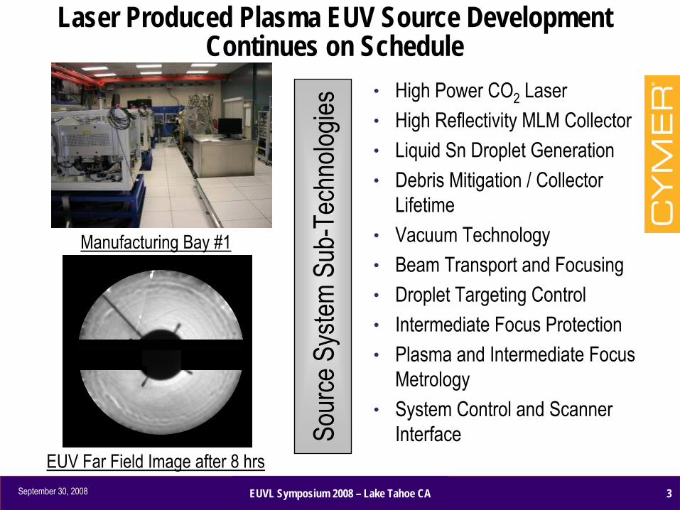
Laser Produced Plasma EUV Source Development Continues on Schedule
h
High Power CO2
Laserh
High Reflectivity MLM Collectorh
Liquid Sn
Droplet Generationh
Debris Mitigation / Collector Lifetime
h
Vacuum Technologyh
Beam Transport and Focusingh
Droplet Targeting Controlh
Intermediate Focus Protectionh
Plasma and Intermediate Focus Metrology
h
System Control and Scanner InterfaceSo
urce
Sys
tem S
ub-T
echn
ologie
s
Manufacturing Bay #1
EUV Far Field Image after 8 hrs
7March 2, 2005 5751-26 Emerging Lithographic Technologies IX, Microlithography 2005, San Jose, California
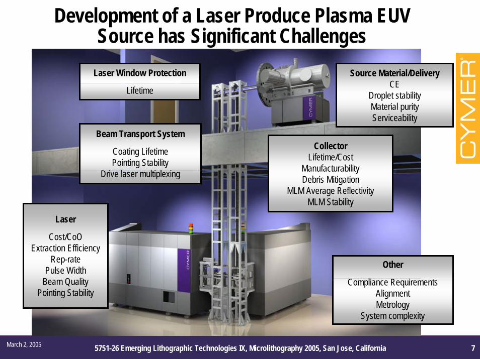
Development of a Laser Produce Plasma EUV Source has Significant Challenges
Laser
Cost/CoOExtraction Efficiency
Rep-ratePulse Width
Beam QualityPointing Stability
Beam Transport System
Coating LifetimePointing Stability
Drive laser multiplexing
Source Material/DeliveryCE
Droplet stabilityMaterial purityServiceability
Laser Window Protection
Lifetime
CollectorLifetime/Cost
ManufacturabilityDebris Mitigation
MLM Average ReflectivityMLM Stability
Other
Compliance RequirementsAlignmentMetrology
System complexity
11March 2, 2005 5751-26 Emerging Lithographic Technologies IX, Microlithography 2005, San Jose, California
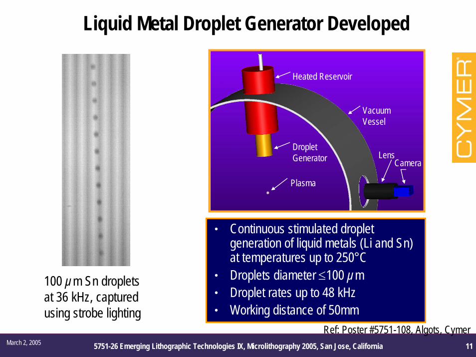
Liquid Metal Droplet Generator Developed
Heated Reservoir
Droplet Generator
Vacuum Vessel
Lens
Plasma
Camera
h Continuous stimulated droplet generation of liquid metals (Li and Sn) at temperatures up to 250°C
h Droplets diameter ≤100 µmh Droplet rates up to 48 kHzh Working distance of 50mm
100 µm Sn droplets at 36 kHz, captured using strobe lighting
Ref: Poster #5751-108, Algots, Cymer
19EUVL Symposium 2008 – Lake Tahoe CASeptember 30, 2008
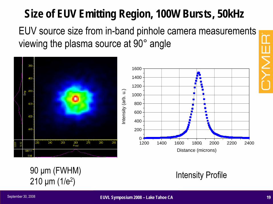
Size of EUV Emitting Region, 100W Bursts, 50kHzEUV source size from in-band pinhole camera measurements viewing the plasma source at 90°
angle
90 μm (FWHM)210 μm (1/e2)
Intensity Profile
1200 1400 1600 1800 2000 2200 24000
200
400
600
800
1000
1200
1400
1600
Inte
nsity
(arb
. u.)
Distance (microns)
5EUVL Symposium 2008 – Lake Tahoe CASeptember 30, 2008
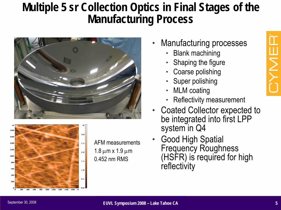
Multiple 5 sr Collection Optics in Final Stages of the Manufacturing Process
h
Manufacturing processesh
Blank machiningh
Shaping the figureh
Coarse polishingh
Super polishingh
MLM coatingh
Reflectivity measurementh
Coated Collector expected to be integrated into first LPP system in Q4
h
Good High Spatial Frequency Roughness (HSFR) is required for high reflectivity
AFM measurements1.8 μm x 1.9 μm0.452 nm RMS
13March 2, 2005 5751-26 Emerging Lithographic Technologies IX, Microlithography 2005, San Jose, California
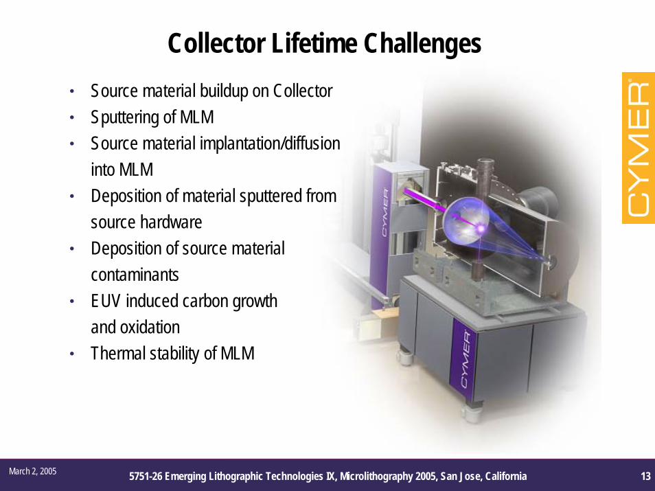
Collector Lifetime Challengesh Source material buildup on Collectorh Sputtering of MLMh Source material implantation/diffusion
into MLMh Deposition of material sputtered from
source hardwareh Deposition of source material
contaminantsh EUV induced carbon growth
and oxidationh Thermal stability of MLM
10EUVL Symposium 2008 – Lake Tahoe CASeptember 30, 2008October 14, 2008©
Copyright 2007 Cymer, Inc.
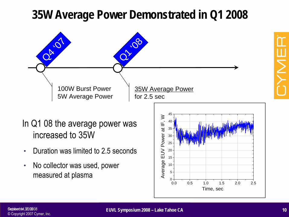
35W Average Power Demonstrated in Q1 2008
In Q1 08 the average power was increased to 35W
h
Duration was limited to 2.5 seconds
h
No collector was used, power measured at plasma
100W Burst Power5W Average Power
Q4 ‘07
35W Average Power for 2.5 sec
Q1 ‘08
0.0 0.5 1.0 1.5 2.0 2.50
5
10
15
20
25
30
35
40
45
Ave
rage
EU
V P
ower
at I
F, W
Time, sec
15EUVL Symposium 2008 – Lake Tahoe CASeptember 30, 2008
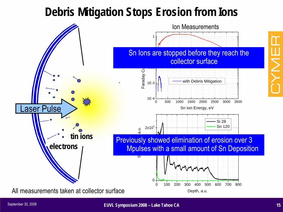
Debris Mitigation Stops Erosion from Ions
tin ionselectrons
Laser Pulse0 500 1000 1500 2000 2500 3000 3500
1E-4
1E-3
0.01
0.1
1
with Debris Mitigation
Fara
day
Cup
Sig
nal,
V
Sn Ion Energy, eV
without Debris Mitigation
Ion Measurements
0 100 200 300 400 500 600 700 8000
1x10⁵
2x10⁵
SIM
S s
igna
l, a.
u.
Depth, a.u.
Si 28 Sn 120
Sn
Ions are stopped before they reach the collector surface
Previously showed elimination of erosion over 3 Mpulses
with a small amount of Sn
Deposition
All measurements taken at collector surface
20EUVL Symposium 2008 – Lake Tahoe CASeptember 30, 2008
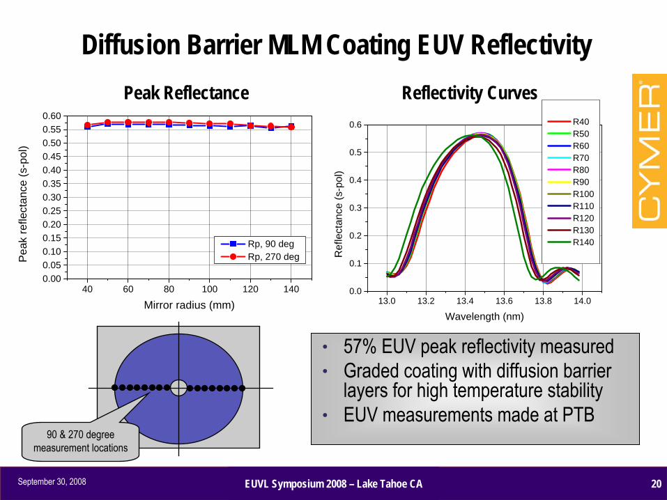
Diffusion Barrier MLM Coating EUV Reflectivity
h
57% EUV peak reflectivity measured h
Graded coating with diffusion barrier layers for high temperature stability
h
EUV measurements made at PTB
Peak Reflectance Reflectivity Curves
13.0 13.2 13.4 13.6 13.8 14.00.0
0.1
0.2
0.3
0.4
0.5
0.6 R40 R50 R60 R70 R80 R90 R100 R110 R120 R130 R140
Ref
lect
ance
(s-p
ol)
Wavelength (nm)
40 60 80 100 120 1400.000.050.100.150.200.250.300.350.400.450.500.550.60
Rp, 90 deg Rp, 270 degPea
k re
flect
ance
(s-p
ol)
Mirror radius (mm)
90 & 270 degree measurement locations
16EUVL Symposium 2008 – Lake Tahoe CASeptember 30, 2008
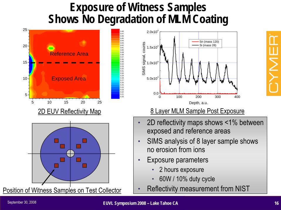
Exposure of Witness Samples Shows No Degradation of MLM Coating
h
2D reflectivity maps shows <1% between exposed and reference areas
h
SIMS analysis of 8 layer sample shows no erosion from ions
h
Exposure parametersh
2 hours exposureh
60W / 10% duty cycleh
Reflectivity measurement from NIST
5 10 15 20 25
5
10
15
20
25
0.200.210.220.230.240.250.260.270.280.290.300.310.320.330.340.350.360.370.380.390.400.410.420.430.440.450.460.470.48
Exposed Area
Reference Area
0 100 200 300 4000.0
5.0x10³
1.0x10⁴
1.5x10⁴
2.0x10⁴
SIM
S s
igna
l, co
unts
Depth, a.u.
Sn (mass 120) Si (mass 28)
2D EUV Reflectivity Map 8 Layer MLM Sample Post Exposure
Position of Witness Samples on Test Collector
23EUVL Symposium 2008 – Lake Tahoe CASeptember 30, 2008
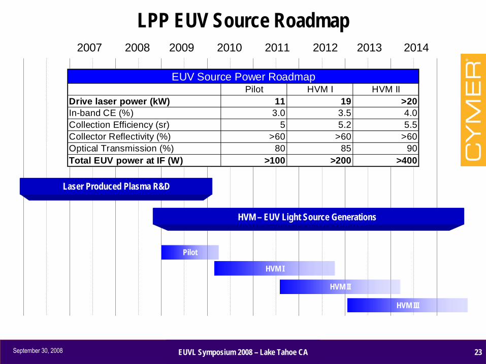
2007 2008 2009 2010 2011 2012 2013 2014
Laser Produced Plasma R&D
HVM – EUV Light Source Generations
Pilot
HVM I
HVM II
HVM III
LPP EUV Source Roadmap
Pilot HVM I HVM IIDrive laser power (kW) 11 19 >20In-band CE (%) 3.0 3.5 4.0Collection Efficiency (sr) 5 5.2 5.5Collector Reflectivity (%) >60 >60 >60Optical Transmission (%) 80 85 90Total EUV power at IF (W) >100 >200 >400
EUV Source Power Roadmap
24EUVL Symposium 2008 – Lake Tahoe CASeptember 30, 2008
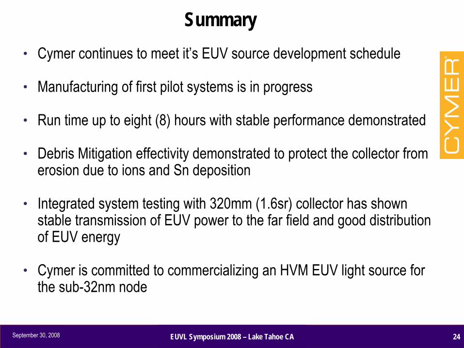
Summaryh
Cymer continues to meet it’s EUV source development schedule
h
Manufacturing of first pilot systems is in progress
h
Run time up to eight (8) hours with stable performance demonstrated
h
Debris Mitigation effectivity demonstrated to protect the collector from erosion due to ions and Sn
deposition
h
Integrated system testing with 320mm (1.6sr) collector has shown stable transmission of EUV power to the far field and good distribution
of EUV energy
h
Cymer is committed to commercializing an HVM EUV light source for the sub-32nm node
SPIE 2009, San Jose, February 24, 2009
Philips’s EUV Source:
Update and Issues
J. Pankert, EUV Source Workshop San Jose 2005
Sn DPP source-collector modules:
Status of Alpha sources, Beta developments, and
HVM experiments
Marc Corthout, Masaki Yoshioka, et al.
SPIE Advanced Lithography San Jose, February 24, 2009
Philips Extreme UV
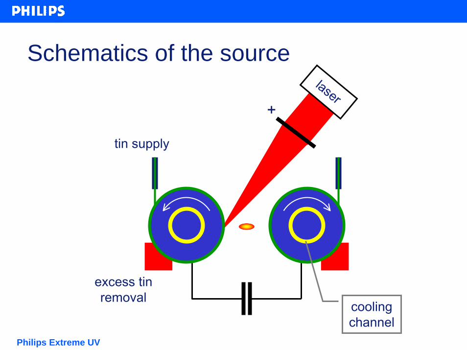
Schematics of the source
+
laser
tin supply
excess tinremoval
cooling channel
SPIE 2009, San Jose, February 24, 2009
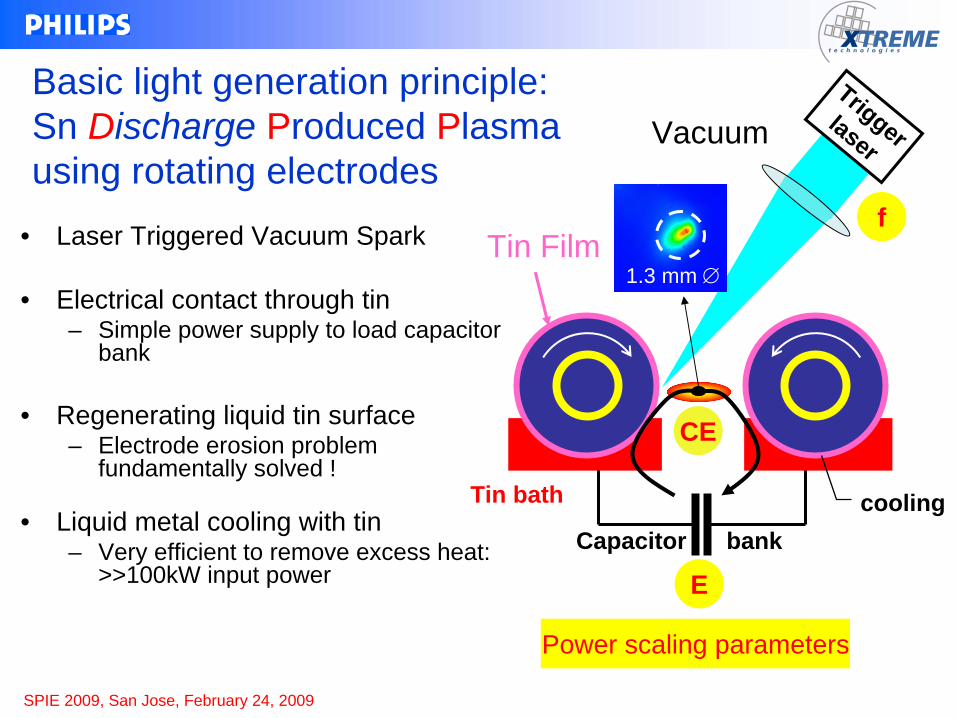
Basic light generation principle: Sn Discharge Produced Plasma using rotating electrodes
• Laser Triggered Vacuum Spark
• Electrical contact through tin – Simple power supply to load capacitor
bank
• Regenerating liquid tin surface– Electrode erosion problem
fundamentally solved !
• Liquid metal cooling with tin– Very efficient to remove excess heat:
>>100kW input power
Tin bath
Capacitor bank
TriggerlaserVacuum
Tin Film
cooling
1.3 mm
Power scaling parameters
E
CE
f
SPIE 2009, San Jose, February 24, 2009
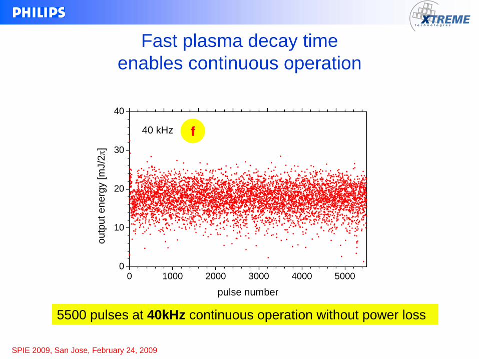
Fast plasma decay time enables continuous operation
0 1000 2000 3000 4000 50000
10
20
30
400.00 0.02 0.04 0.06 0.08 0.10 0.12
40 kHz
outp
ut e
nerg
y [m
J/2
]
pulse number
time [s]
5500 pulses at 40kHz continuous operation without power loss
f

Philips Extreme UV
Summary of the properties• Electrodes
– Rotating: scalability to very high powers– Regenerative electrodes:
• Liquid tin surface• Erosion problem fundamentally solved
• General properties– CE 2%– Pinch size < 1mm– 5 kHz demonstrated– 120 W continuous operation– 260 W short term (limited by vacuum vessel)
SPIE 2009, San Jose, February 24, 2009
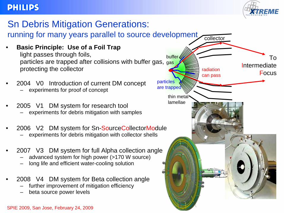
radiation can pass
buffergas
particles are trapped
collector
thin metal lamellae
Sn Debris Mitigation Generations: running for many years parallel to source development• Basic Principle: Use of a Foil Trap
light passes through foils,particles are trapped after collisions with buffer gas,protecting the collector
• 2004 V0 Introduction of current DM concept– experiments for proof of concept
• 2005 V1 DM system for research tool– experiments for debris mitigation with samples
• 2006 V2 DM system for Sn-SourceCollectorModule– experiments for debris mitigation with collector shells
• 2007 V3 DM system for full Alpha collection angle– advanced system for high power (>170 W source)– long life and efficient water-cooling solution
• 2008 V4 DM system for Beta collection angle– further improvement of mitigation efficiency– beta source power levels
ToIntermediate
Focus
SPIE 2009, San Jose, February 24, 2009
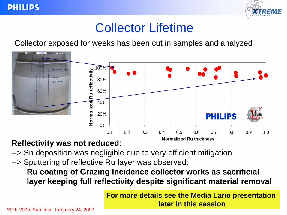
0%
20%
40%
60%
80%
100%
0.1 0.2 0.3 0.4 0.5 0.6 0.7 0.8 0.9 1.0Normalized Ru thickness
No
rma
lized
Ru
ref
lec
tivity
Collector LifetimeCollector exposed for weeks has been cut in samples and analyzed
Reflectivity was not reduced:--> Sn deposition was negligible due to very efficient mitigation--> Sputtering of reflective Ru layer was observed:
Ru coating of Grazing Incidence collector works as sacrificial layer keeping full reflectivity despite significant material removal
For more details see the Media Lario presentation later in this session
SPIE 2009, San Jose, February 24, 2009
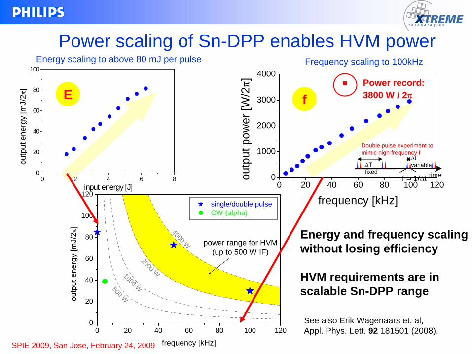
Energy scaling to above 80 mJ per pulse
0 2 4 6 80
20
40
60
80
100
outp
ut e
nerg
y [m
J/2
]
input energy [J]
Frequency scaling to 100kHz
timeT fixed
t variable
f = 1/t
Double pulse experiment to mimic high frequency f
0 20 40 60 80 100 1200
1000
2000
3000
4000
outp
ut p
ower
[W/2]
frequency [kHz]
Power record:3800 W / 2
0 20 40 60 80 100 1200
20
40
60
80
100
120 single/double pulse CW (alpha)
power range for HVM(up to 500 W IF)
2000 W1000 W500 W
4000 W
outp
ut e
nerg
y [m
J/2
]
frequency [kHz]
Energy and frequency scaling without losing efficiency
HVM requirements are in scalable Sn-DPP range
Power scaling of Sn-DPP enables HVM power
See also Erik Wagenaars et. al,Appl. Phys. Lett. 92 181501 (2008).
E f
SPIE 2009, San Jose, February 24, 2009
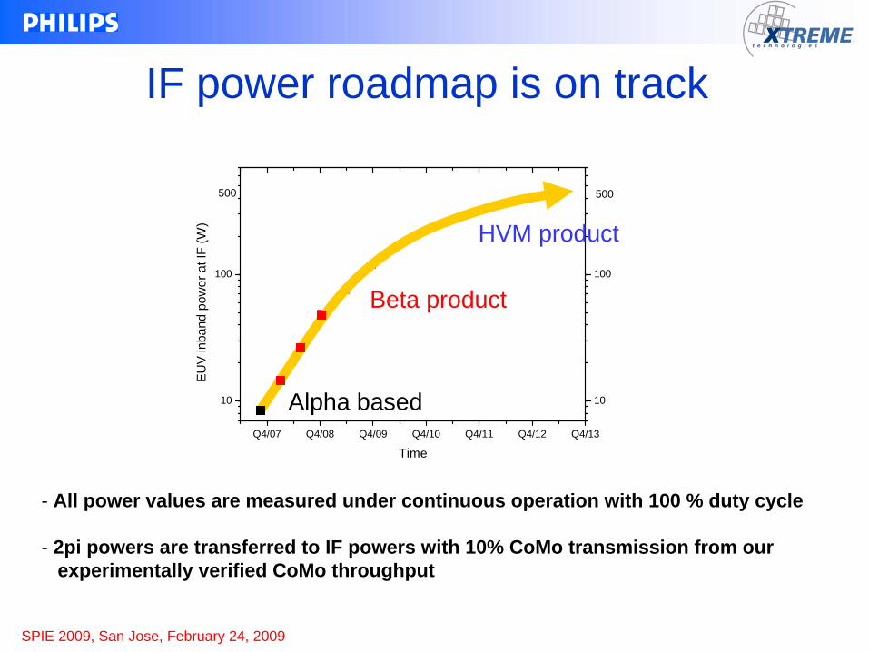
IF power roadmap is on track
- All power values are measured under continuous operation with 100 % duty cycle
- 2pi powers are transferred to IF powers with 10% CoMo transmission from our experimentally verified CoMo throughput
Q4/07 Q4/08 Q4/09 Q4/10 Q4/11 Q4/12 Q4/13
10
100
10
100
EU
V in
band
pow
er a
t IF
(W)
Time
Alpha based
Beta product
500500
HVM product
EUV Sources for Lithography (SPIE, November 2005)Vivek Bakshi, Editor
This comprehensive volume, edited by a senior technical staff member at SEMATECH, is the authoritative reference book on EUV source technology. The volume contains 38 chapters contributed by leading researchers and suppliers in the EUV source field. Topics range from a state-of-the-art overview and in-depth explanation of EUV source requirements, to fundamental atomic data and theoretical models of EUV sources based on discharge-produced plasmas (DPPs) and laser-produced plasmas (LPPs), to a description of prominent DPP and LPP designs and other technologies for producing EUV radiation. Addi-tional topics include EUV source metrology and components (collectors, electrodes), debris mitigation, and mechanisms of compo-nent erosion in EUV sources. The volume is intended to meet the needs of both practitioners of the technology and readers seeking an introduc-tion to the subject.
Prices: $127 / $150 (SPIE Member/List)(Available November 2005)
EUV LithographyVivek Bakshi, Editor
SPIE.org
Ch06_VUVSpec.ai
Professor David AttwoodAST 210/EECS 213Univ. California, Berkeley