Embed Size (px)
Citation preview
February 2011 Doc ID 18376 Rev 1 1/47
AN3329Application note
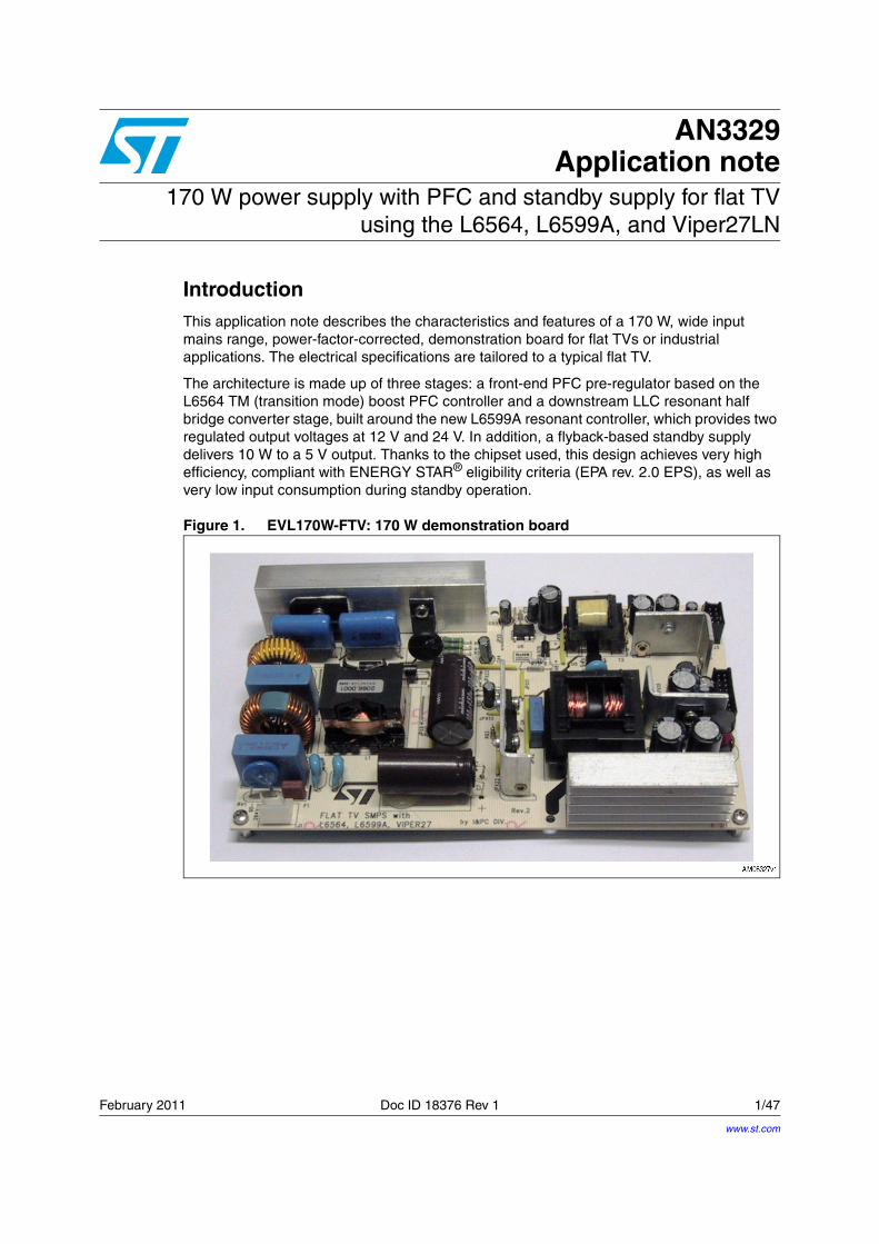
170 W power supply with PFC and standby supply for flat TVusing the L6564, L6599A, and Viper27LN
IntroductionThis application note describes the characteristics and features of a 170 W, wide input mains range, power-factor-corrected, demonstration board for flat TVs or industrial applications. The electrical specifications are tailored to a typical flat TV.
The architecture is made up of three stages: a front-end PFC pre-regulator based on the L6564 TM (transition mode) boost PFC controller and a downstream LLC resonant half bridge converter stage, built around the new L6599A resonant controller, which provides two regulated output voltages at 12 V and 24 V. In addition, a flyback-based standby supply delivers 10 W to a 5 V output. Thanks to the chipset used, this design achieves very high efficiency, compliant with ENERGY STAR® eligibility criteria (EPA rev. 2.0 EPS), as well as very low input consumption during standby operation.
Figure 1. EVL170W-FTV: 170 W demonstration board
www.st.com
Contents AN3329
2/47 Doc ID 18376 Rev 1
Contents
1 Main characteristics and circuit description . . . . . . . . . . . . . . . . . . . . . 6
2 Efficiency measurement . . . . . . . . . . . . . . . . . . . . . . . . . . . . . . . . . . . . . . 9
3 Harmonic content measurement . . . . . . . . . . . . . . . . . . . . . . . . . . . . . . 11
4 Functional check . . . . . . . . . . . . . . . . . . . . . . . . . . . . . . . . . . . . . . . . . . . 13
5 Conducted emission pre-compliance test . . . . . . . . . . . . . . . . . . . . . . 29
6 Bill of materials . . . . . . . . . . . . . . . . . . . . . . . . . . . . . . . . . . . . . . . . . . . . 31
7 PFC coil specifications . . . . . . . . . . . . . . . . . . . . . . . . . . . . . . . . . . . . . . 39
8 Resonant power transformer specifications . . . . . . . . . . . . . . . . . . . . 41
9 Auxiliary flyback transformer specifications . . . . . . . . . . . . . . . . . . . . 43
10 Revision history . . . . . . . . . . . . . . . . . . . . . . . . . . . . . . . . . . . . . . . . . . . 46

AN3329 List of tables
Doc ID 18376 Rev 1 3/47
List of tables
Table 1. Overall efficiency measured at different AC input voltages . . . . . . . . . . . . . . . . . . . . . . . . . 9Table 2. Bill of materials . . . . . . . . . . . . . . . . . . . . . . . . . . . . . . . . . . . . . . . . . . . . . . . . . . . . . . . . . . 31Table 3. PFC coil winding data . . . . . . . . . . . . . . . . . . . . . . . . . . . . . . . . . . . . . . . . . . . . . . . . . . . . . 39Table 4. Resonant transformer winding data . . . . . . . . . . . . . . . . . . . . . . . . . . . . . . . . . . . . . . . . . . 41Table 5. DC output voltage and load . . . . . . . . . . . . . . . . . . . . . . . . . . . . . . . . . . . . . . . . . . . . . . . . 43Table 6. Standby transformer winding data . . . . . . . . . . . . . . . . . . . . . . . . . . . . . . . . . . . . . . . . . . . 44Table 7. Document revision history . . . . . . . . . . . . . . . . . . . . . . . . . . . . . . . . . . . . . . . . . . . . . . . . . 46
List of figures AN3329
4/47 Doc ID 18376 Rev 1
List of figures
Figure 1. EVL170W-FTV: 170 W demonstration board . . . . . . . . . . . . . . . . . . . . . . . . . . . . . . . . . . . . 1Figure 2. Electrical diagram . . . . . . . . . . . . . . . . . . . . . . . . . . . . . . . . . . . . . . . . . . . . . . . . . . . . . . . . . 8Figure 3. Overall efficiency vs. output power . . . . . . . . . . . . . . . . . . . . . . . . . . . . . . . . . . . . . . . . . . . 10Figure 4. Average efficiency acc. ES-2 . . . . . . . . . . . . . . . . . . . . . . . . . . . . . . . . . . . . . . . . . . . . . . . 10Figure 5. Standby supply efficiency vs. output power . . . . . . . . . . . . . . . . . . . . . . . . . . . . . . . . . . . . 10Figure 6. Standby supply efficiency vs. light load output power . . . . . . . . . . . . . . . . . . . . . . . . . . . . 10Figure 7. EN61000-3-2 compliance at 230 Vac - 50 Hz, full load . . . . . . . . . . . . . . . . . . . . . . . . . . . 11Figure 8. JEITA-MITI compliance at 100 Vac - 50 Hz, full load . . . . . . . . . . . . . . . . . . . . . . . . . . . . . 11Figure 9. EN61000-3-2 compliance at 230 Vac - 50 Hz, 75 W . . . . . . . . . . . . . . . . . . . . . . . . . . . . . 11Figure 10. JEITA-MITI compliance at 100 Vac - 50 Hz, 75 W . . . . . . . . . . . . . . . . . . . . . . . . . . . . . . . 11Figure 11. Input voltage and current at 100 Vac, full load . . . . . . . . . . . . . . . . . . . . . . . . . . . . . . . . . . 12Figure 12. Input voltage and current at 230 Vac, full load . . . . . . . . . . . . . . . . . . . . . . . . . . . . . . . . . . 12Figure 13. Standby supply waveforms at 115 Vac - 60 Hz, full load . . . . . . . . . . . . . . . . . . . . . . . . . . 13Figure 14. Standby supply waveforms at 230 Vac - 50 Hz, full load . . . . . . . . . . . . . . . . . . . . . . . . . . 13Figure 15. Standby supply waveforms at 400 Vdc, full load . . . . . . . . . . . . . . . . . . . . . . . . . . . . . . . . 14Figure 16. Standby supply output rectifiers PIV at 400 Vdc, full load . . . . . . . . . . . . . . . . . . . . . . . . . 14Figure 17. Standby supply 5 V ripple at 115 Vac - 60 Hz, full load . . . . . . . . . . . . . . . . . . . . . . . . . . . 14Figure 18. Standby supply startup at 115 Vac - 60 Hz, full load . . . . . . . . . . . . . . . . . . . . . . . . . . . . . 14Figure 19. Standby supply burst mode operation at 230 Vac - 50 Hz - 10 mA load . . . . . . . . . . . . . . 15Figure 20. Standby supply burst mode operation at 230 Vac - 50 Hz - 10 mA load-detail . . . . . . . . . 15Figure 21. Standby supply OVP at 115 Vac - 60 Hz, full load . . . . . . . . . . . . . . . . . . . . . . . . . . . . . . . 15Figure 22. Standby supply OVP at 230 Vac - 50 Hz - 0.5 A . . . . . . . . . . . . . . . . . . . . . . . . . . . . . . . . 15Figure 23. Standby supply OVP at 115 Vac - 60 Hz - PFC on - 1 A . . . . . . . . . . . . . . . . . . . . . . . . . . 16Figure 24. Standby supply OVP at 115 Vac - 60 Hz - PFC on - 1 A . . . . . . . . . . . . . . . . . . . . . . . . . . 16Figure 25. Standby supply output short-circuit at 230 Vac - 50 Hz, full load . . . . . . . . . . . . . . . . . . . . 16Figure 26. Standby supply output short-circuit at 230 Vac - 50 Hz, full load - detail . . . . . . . . . . . . . . 16Figure 27. Standby supply dynamic load at 115 Vac - 60 Hz - PFC off . . . . . . . . . . . . . . . . . . . . . . . . 17Figure 28. Standby supply dynamic load at 115 Vac - 60 Hz - PFC on. . . . . . . . . . . . . . . . . . . . . . . . 17Figure 29. PFC Vds and inductor current at 115 Vac - 60 Hz, full load . . . . . . . . . . . . . . . . . . . . . . . . 18Figure 30. PFC Vds and inductor current at 115 Vac - 60 Hz, full load - detail . . . . . . . . . . . . . . . . . . 18Figure 31. PFC Vds and inductor current at 230 Vac - 50 Hz, full load . . . . . . . . . . . . . . . . . . . . . . . . 19Figure 32. PFC Vds and inductor current at 230 Vac - 50 Hz, full load - detail . . . . . . . . . . . . . . . . . . 19Figure 33. L6564 signals-1 at 115 Vac - 60 Hz, full load . . . . . . . . . . . . . . . . . . . . . . . . . . . . . . . . . . . 19Figure 34. L6564 signals-2 at 115 Vac - 60 Hz, full load . . . . . . . . . . . . . . . . . . . . . . . . . . . . . . . . . . . 19Figure 35. PFC signals-1 at 115 Vac - 60 Hz, full load . . . . . . . . . . . . . . . . . . . . . . . . . . . . . . . . . . . . 20Figure 36. PFC signals-2 at 115 Vac - 60 Hz, full load . . . . . . . . . . . . . . . . . . . . . . . . . . . . . . . . . . . . 20Figure 37. Resonant stage waveforms at 115 V - 60 Hz, full load. . . . . . . . . . . . . . . . . . . . . . . . . . . . 21Figure 38. Resonant stage waveforms at 115 V - 60 Hz, full load. . . . . . . . . . . . . . . . . . . . . . . . . . . . 21Figure 39. Output rectifiers PIV waveforms . . . . . . . . . . . . . . . . . . . . . . . . . . . . . . . . . . . . . . . . . . . . . 22Figure 40. No load operation at 115 Vac - 60 Hz. . . . . . . . . . . . . . . . . . . . . . . . . . . . . . . . . . . . . . . . . 22Figure 41. No load operation at 115 Vac - 60 Hz - L6599A signals . . . . . . . . . . . . . . . . . . . . . . . . . . . 22Figure 42. 12 V - 2 A; 24 V 0 ÷ 6 A transition at 115 Vac - 60 Hz . . . . . . . . . . . . . . . . . . . . . . . . . . . . 23Figure 43. 24 V - 6 A; 12 V 0 ÷ 2 A transition at 115 Vac - 60 Hz . . . . . . . . . . . . . . . . . . . . . . . . . . . . 23Figure 44. 12 V - 2 A; 24 V 0 ÷ 6 A - 300 Hz transition at 115 Vac - 60 Hz . . . . . . . . . . . . . . . . . . . . . 24Figure 45. 24 V - 6 A; 12 V 1 ÷ 2 A - 300 Hz transition at 115 Vac - 60 Hz . . . . . . . . . . . . . . . . . . . . . 24Figure 46. 12 V short-circuit at full load and 115 Vac - 60 Hz . . . . . . . . . . . . . . . . . . . . . . . . . . . . . . . 25Figure 47. 12 V short-circuit at full load and 115 Vac - 60 Hz - detail . . . . . . . . . . . . . . . . . . . . . . . . . 25Figure 48. 24 V short-circuit at full load and 115 Vac - 60 Hz . . . . . . . . . . . . . . . . . . . . . . . . . . . . . . . 25Figure 49. 24 V short-circuit at full load and 115 Vac - 60 Hz - detail . . . . . . . . . . . . . . . . . . . . . . . . . 25
AN3329 List of figures
Doc ID 18376 Rev 1 5/47
Figure 50. Startup by on-off signal at full load and 115 Vac - 60 Hz . . . . . . . . . . . . . . . . . . . . . . . . . . 26Figure 51. Startup by on-off signal at full load and 115 Vac - 60 Hz - L6599A signals . . . . . . . . . . . . 26Figure 52. Startup by on/off signal at full load and 115 Vac - 60 Hz O/P voltage rising . . . . . . . . . . . 27Figure 53. Turn-off at full load and 115 Vac - 60 Hz by on/off signal . . . . . . . . . . . . . . . . . . . . . . . . . . 27Figure 54. OVP at full load and 115 Vac - 60 Hz on 12 V - 24 V . . . . . . . . . . . . . . . . . . . . . . . . . . . . . 27Figure 55. OVP at full load and 115 Vac - 60 Hz on 12 V - 24 V - outputs detail . . . . . . . . . . . . . . . . 27Figure 56. Half cycle mains dip at full load and 115 Vac - 60 Hz. . . . . . . . . . . . . . . . . . . . . . . . . . . . . 28Figure 57. Full cycle mains dip at full load and 115 Vac - 60 Hz . . . . . . . . . . . . . . . . . . . . . . . . . . . . . 28Figure 58. CE peak measurement at 115 V - 60 Hz and full load - phase wire . . . . . . . . . . . . . . . . . . 29Figure 59. CE peak measurement at 115 V - 60 Hz and full load - neutral wire . . . . . . . . . . . . . . . . . 29Figure 60. CE peak measurement at 230 V - 50 Hz and full load - phase wire . . . . . . . . . . . . . . . . . . 30Figure 61. CE peak measurement at 230 V - 50 Hz and full load - neutral wire . . . . . . . . . . . . . . . . . 30Figure 62. PFC coil electrical diagram . . . . . . . . . . . . . . . . . . . . . . . . . . . . . . . . . . . . . . . . . . . . . . . . . 39Figure 63. PFC coil mechanical aspect . . . . . . . . . . . . . . . . . . . . . . . . . . . . . . . . . . . . . . . . . . . . . . . . 40Figure 64. Transformer overall drawing . . . . . . . . . . . . . . . . . . . . . . . . . . . . . . . . . . . . . . . . . . . . . . . . 41Figure 65. Transformer electrical diagram . . . . . . . . . . . . . . . . . . . . . . . . . . . . . . . . . . . . . . . . . . . . . . 42Figure 66. Transformer construction . . . . . . . . . . . . . . . . . . . . . . . . . . . . . . . . . . . . . . . . . . . . . . . . . . 44Figure 67. Mechanical aspect and pin numbering . . . . . . . . . . . . . . . . . . . . . . . . . . . . . . . . . . . . . . . . 44Figure 68. Mechanical aspect and pin numbering . . . . . . . . . . . . . . . . . . . . . . . . . . . . . . . . . . . . . . . . 45
Main characteristics and circuit description AN3329
6/47 Doc ID 18376 Rev 1
1 Main characteristics and circuit description
The main features of the SMPS are:
● Universal input mains range: 90 ÷ 264 Vac - frequency 45 ÷ 65 Hz
● Output voltage 1: 24 V ± 5 % at 6 A for backlight and audio supply
● Output voltage 2: 12 V ± 3 % at 2 A for TV panel supply
● Output voltage 3: 5 V ± 2 % at 2 A for microprocessor supply
● Mains harmonics: acc. to EN61000-3-2 Class-D or JEITA-MITI Class-D
● Standby mains consumption: at 230 Vac <150 mW with 50 mW load
● Overall efficiency at full load: above 90 %
● EMI: according to EN55022-Class-B
● Safety: according to EN60065
● Dimensions: 197x115 mm, 25 mm maximum component height from PCB
● PCB: single side, 70 µm, CEM-1, mixed PTH/SMT.
The circuit is made up of two sections; a 10 W supply generating 5 V standby output, dedicated to supplying the TV microprocessor and the logic circuitry, and a larger section made up of a PFC front-end and an LLC resonant converter which provides two output voltages, one dedicated to supplying the TV panel, and one for the backlight and audio power amplifiers. The PFC stage delivers 400 V constant voltage and acts as a pre-regulator for both the LLC stage and the standby supply. An external signal, referred to as secondary ground, turns the PFC and LLC stages on and off.
Startup
At turn-on the standby supply starts up and delivers 5 V dedicated to the TV microprocessor and other logic circuitry. It also generates the auxiliary supply voltage for the PFC and LLC controllers at primary side via the linear regulator Q7. Q7 is activated by the optocoupler U5, that is driven by the logic signal on/off (active high). At startup, the on/off signal (delivered by the microprocessor) is supposed to be low, so the PFC and the LLC are off. Once the on/off signal is asserted high, the regulator Q7 provides 14 V to the L6564 PFC controller and the L6599A LLC controller; to always ensure proper operation of the LLC, the circuit is designed so that the PFC starts first, then the downstream converter. The LINE pin of L6599A allows the resonant stage to operate only if the PFC output is delivering its rated output voltage. It prevents the resonant converter from working with an input voltage that is too low which may cause the undesirable capacitive-mode operation. The L6599A LINE pin internal comparator has a hysteresis allowing to set the turn-on and turn-off thresholds independently. The LLC turn-on voltage (PFC output) and the turn-off threshold are set to 380 V and 300 V respectively. This last value prevents the LLC stage operating in capacitive-mode but allows the resonant stage to operate even in the case of mains sag or dips lowering the PFC output voltage.
Brownout protection
Brownout protection prevents the circuit from working with abnormal mains levels. It is accomplished by both the Viper, through the brownout pin, and the L6564, through an internal comparator internally connected to the VFF pin (#5), which detects the mains voltage peak value. The internal comparators allow the IC operation with proper mains level only, as defined by power supply specifications, therefore, if the input voltage is below around 80 Vac (typ.), the circuit is not allowed to start up.
AN3329 Main characteristics and circuit description
Doc ID 18376 Rev 1 7/47
Resonant power stage
The downstream converter features the ST L6599A, which embeds all the functions needed to drive properly the resonant converter with 50 % fixed duty cycle and variable frequency. The converter makes use of a transformer designed with the integrated magnetic approach, using the primary leakage as the resonant series inductance and the magnetizing inductance as the resonant shunt inductance. The transformer secondary-side is center-tapped and power Schottky diodes are used as output rectifiers. Additional LC filter stages have been added on each output to minimize high-frequency ripple.
Output voltage feedback loop
The regulation feedback loop is implemented through a typical circuit using a TL431, which modulates the current through the optocoupler diode. In order to improve the cross regulation, the two resonant stage output voltages are regulated by a weighted feedback control, that is using a single rail to regulate multiple outputs. The feedback loop is closed to the primary side by R37, which connects the RFMIN (#4) pin of the resonant controller L6599A to the optocoupler phototransistor and sets the maximum switching frequency at around 130 kHz. This value has been chosen to limit the switching losses at light load operation. On the same pin, R36 connected to ground, sets the minimum switching frequency. The RC series R22 and C21 sets both soft-start maximum frequency as well as duration.
L6599A overload and short-circuit protection
Half bridge primary-side current is sensed by the lossless circuit consisting of R53, C36, D14, D12, R55, and C38 and is fed into the ISEN pin (#6). During an overcurrent event, the pin voltage rises to the internal comparator threshold (0.8 V), triggering the following protection sequence: the soft-start capacitor (C10) connected to the DELAY pin (#2) is charged by an internal 150 µA current generator and is slowly discharged by the resistor R12. This pin is connected to the DIS (#8) pin and, if the voltage reaches 1.85 V, the IC stops switching, being latched off. Once latched, an on/off signal recycle is needed to restart the converter.
Overvoltage and open loop protection
Both PFC and resonant stages are provided with their own overvoltage protections. The PFC controller L6564 monitors its output voltage through the resistor divider connected to the PFC_OK pin (#6) protecting the circuit in case of loop failure, disconnection, or deviation from the nominal value of the feedback loop divider. When a fault condition is detected, the L6564 is shut down and latched off by an internal circuit monitoring the voltage on the PFC_OK and INV pins, until the mains voltage is recycled. Upon the occurrence of an overvoltage condition, of either the 24 V or 12 V output of the resonant stage, the Zener diodes D16 and D17 conduct, respectively, forcing Q10 to be turned on by the resulting base current, which causes Q9 to conduct. These two transistors form a pnp-npn SCR (silicon controlled rectifier) structure that shorts to ground the anode of the U5 optocoupler in such a way that the IC supply voltage Vcc cannot be delivered to controllers by Q7, forcing them to be latched off until the mains voltage is recycled.
Main characteristics and circuit description AN3329
8/47 Doc ID 18376 Rev 1
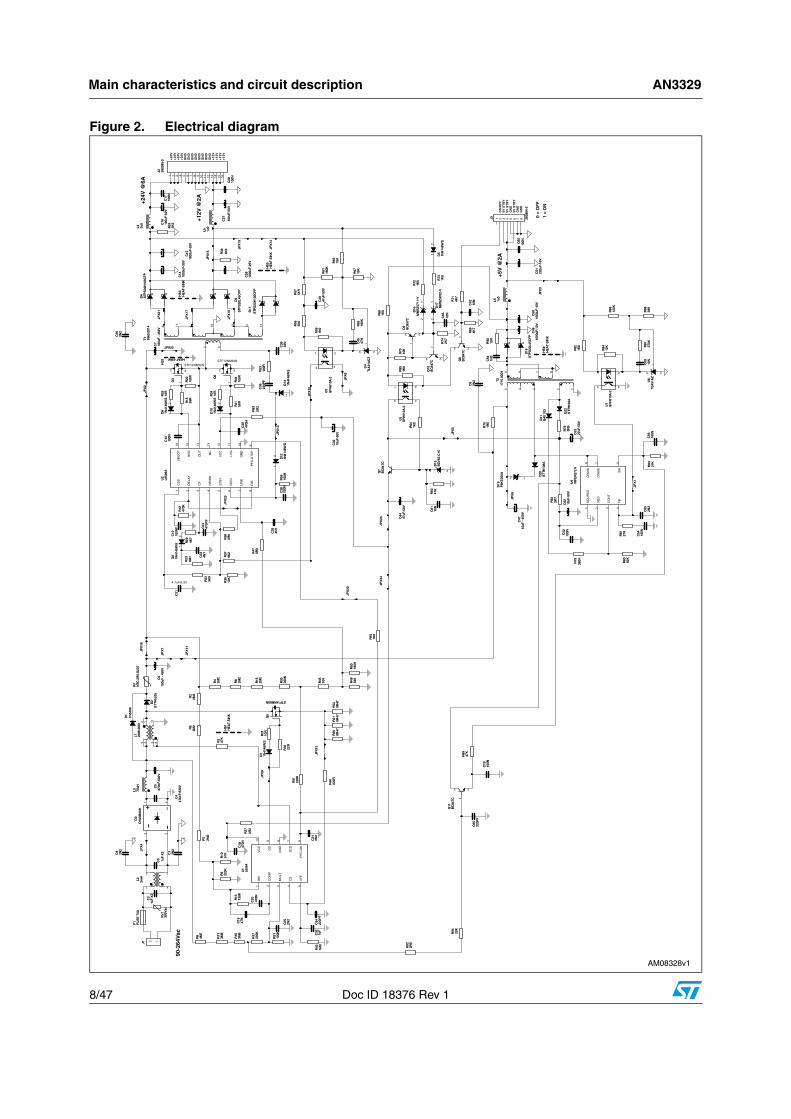
Figure 2. Electrical diagram
AN3329 Efficiency measurement
Doc ID 18376 Rev 1 9/47
2 Efficiency measurement
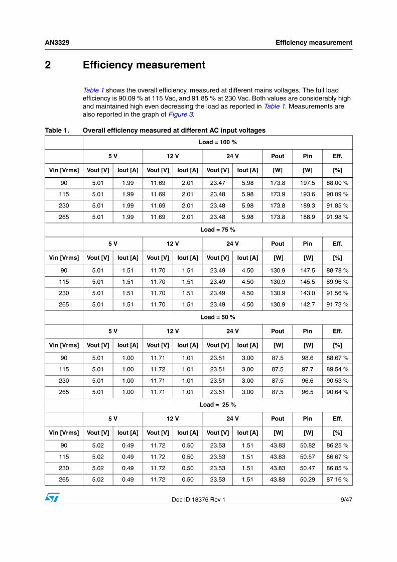
Table 1 shows the overall efficiency, measured at different mains voltages. The full load efficiency is 90.09 % at 115 Vac, and 91.85 % at 230 Vac. Both values are considerably high and maintained high even decreasing the load as reported in Table 1. Measurements are also reported in the graph of Figure 3.
Table 1. Overall efficiency measured at different AC input voltages
Load = 100 %
5 V 12 V 24 V Pout Pin Eff.
Vin [Vrms] Vout [V] Iout [A] Vout [V] Iout [A] Vout [V] Iout [A] [W] [W] [%]
90 5.01 1.99 11.69 2.01 23.47 5.98 173.8 197.5 88.00 %
115 5.01 1.99 11.69 2.01 23.48 5.98 173.9 193.6 90.09 %
230 5.01 1.99 11.69 2.01 23.48 5.98 173.8 189.3 91.85 %
265 5.01 1.99 11.69 2.01 23.48 5.98 173.8 188.9 91.98 %
Load = 75 %
5 V 12 V 24 V Pout Pin Eff.
Vin [Vrms] Vout [V] Iout [A] Vout [V] Iout [A] Vout [V] Iout [A] [W] [W] [%]
90 5.01 1.51 11.70 1.51 23.49 4.50 130.9 147.5 88.78 %
115 5.01 1.51 11.70 1.51 23.49 4.50 130.9 145.5 89.96 %
230 5.01 1.51 11.70 1.51 23.49 4.50 130.9 143.0 91.56 %
265 5.01 1.51 11.70 1.51 23.49 4.50 130.9 142.7 91.73 %
Load = 50 %
5 V 12 V 24 V Pout Pin Eff.
Vin [Vrms] Vout [V] Iout [A] Vout [V] Iout [A] Vout [V] Iout [A] [W] [W] [%]
90 5.01 1.00 11.71 1.01 23.51 3.00 87.5 98.6 88.67 %
115 5.01 1.00 11.72 1.01 23.51 3.00 87.5 97.7 89.54 %
230 5.01 1.00 11.71 1.01 23.51 3.00 87.5 96.6 90.53 %
265 5.01 1.00 11.71 1.01 23.51 3.00 87.5 96.5 90.64 %
Load = 25 %
5 V 12 V 24 V Pout Pin Eff.
Vin [Vrms] Vout [V] Iout [A] Vout [V] Iout [A] Vout [V] Iout [A] [W] [W] [%]
90 5.02 0.49 11.72 0.50 23.53 1.51 43.83 50.82 86.25 %
115 5.02 0.49 11.72 0.50 23.53 1.51 43.83 50.57 86.67 %
230 5.02 0.49 11.72 0.50 23.53 1.51 43.83 50.47 86.85 %
265 5.02 0.49 11.72 0.50 23.53 1.51 43.83 50.29 87.16 %
Efficiency measurement AN3329
10/47 Doc ID 18376 Rev 1
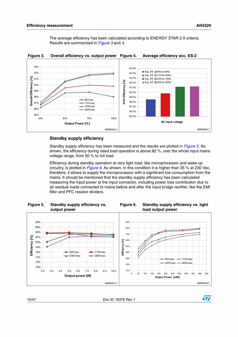
The average efficiency has been calculated according to ENERGY STAR 2.0 criteria. Results are summarized in Figure 3 and 4.
Standby supply efficiency
Standby supply efficiency has been measured and the results are plotted in Figure 5. As shown, the efficiency during rated load operation is above 82 %, over the whole input mains voltage range, from 50 % to full load.
Efficiency during standby operation at very light load, like microprocessor and wake-up circuitry, is plotted in Figure 6. As shown, in this condition it is higher than 35 % at 230 Vac, therefore, it allows to supply the microprocessor with a significant low consumption from the mains. It should be mentioned that the standby supply efficiency has been calculated measuring the input power at the input connector, including power loss contribution due to all residual loads connected to mains before and after the input bridge rectifier, like the EMI filter and PFC resistor dividers.
Figure 3. Overall efficiency vs. output power Figure 4. Average efficiency acc. ES-2
Figure 5. Standby supply efficiency vs. output power
Figure 6. Standby supply efficiency vs. light load output power
AN3329 Harmonic content measurement
Doc ID 18376 Rev 1 11/47
3 Harmonic content measurement
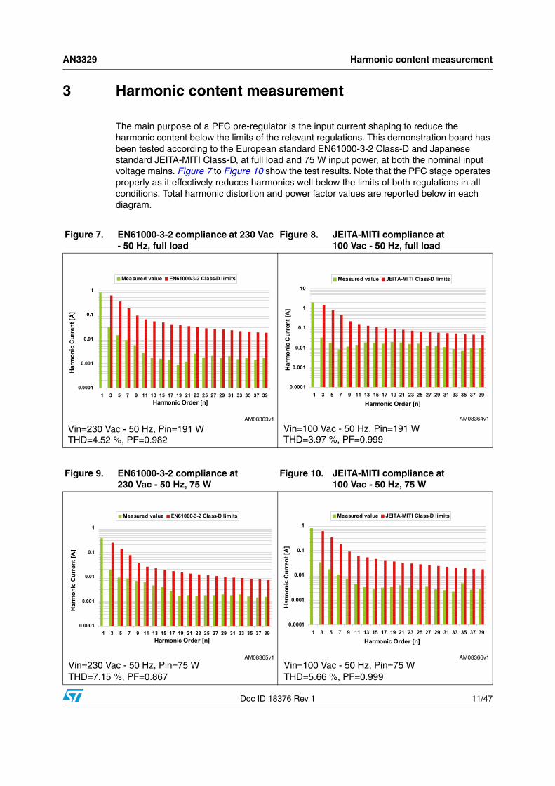
The main purpose of a PFC pre-regulator is the input current shaping to reduce the harmonic content below the limits of the relevant regulations. This demonstration board has been tested according to the European standard EN61000-3-2 Class-D and Japanese standard JEITA-MITI Class-D, at full load and 75 W input power, at both the nominal input voltage mains. Figure 7 to Figure 10 show the test results. Note that the PFC stage operates properly as it effectively reduces harmonics well below the limits of both regulations in all conditions. Total harmonic distortion and power factor values are reported below in each diagram.
Figure 7. EN61000-3-2 compliance at 230 Vac - 50 Hz, full load
Figure 8. JEITA-MITI compliance at 100 Vac - 50 Hz, full load
Vin=230 Vac - 50 Hz, Pin=191 WTHD=4.52 %, PF=0.982
Vin=100 Vac - 50 Hz, Pin=191 WTHD=3.97 %, PF=0.999
Figure 9. EN61000-3-2 compliance at 230 Vac - 50 Hz, 75 W
Figure 10. JEITA-MITI compliance at 100 Vac - 50 Hz, 75 W
Vin=230 Vac - 50 Hz, Pin=75 WTHD=7.15 %, PF=0.867
Vin=100 Vac - 50 Hz, Pin=75 WTHD=5.66 %, PF=0.999
Harmonic content measurement AN3329
12/47 Doc ID 18376 Rev 1
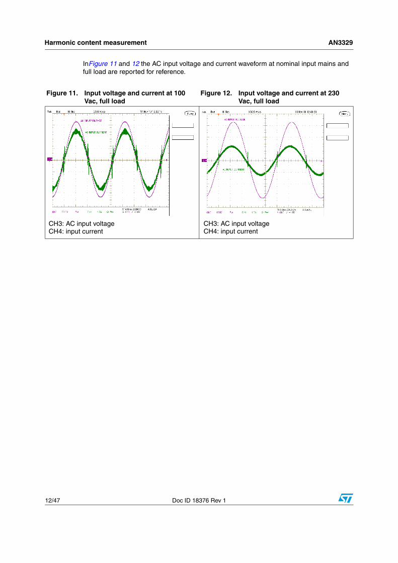
InFigure 11 and 12 the AC input voltage and current waveform at nominal input mains and full load are reported for reference.
Figure 11. Input voltage and current at 100 Vac, full load
Figure 12. Input voltage and current at 230 Vac, full load
CH3: AC input voltageCH4: input current
CH3: AC input voltageCH4: input current
AN3329 Functional check
Doc ID 18376 Rev 1 13/47
4 Functional check
Standby supply
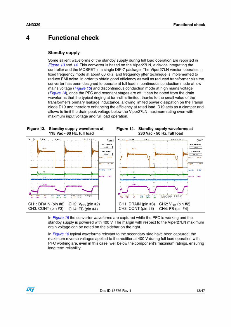
Some salient waveforms of the standby supply during full load operation are reported in Figure 13 and 14. This converter is based on the Viper27LN, a device integrating the controller and the MOSFET in a single DIP-7 package. The Viper27LN version operates in fixed frequency mode at about 60 kHz, and frequency jitter technique is implemented to reduce EMI noise. In order to obtain good efficiency as well as reduced transformer size the converter has been designed to operate at full load in continuous conduction mode at low mains voltage (Figure 13) and discontinuous conduction mode at high mains voltage (Figure 14), once the PFC and resonant stages are off. It can be noted from the drain waveforms that the typical ringing at turn-off is limited, thanks to the small value of the transformer's primary leakage inductance, allowing limited power dissipation on the Transil diode D19 and therefore enhancing the efficiency at rated load. D19 acts as a clamper and allows to limit the drain peak voltage below the Viper27LN maximum rating even with maximum input voltage and full load operation.
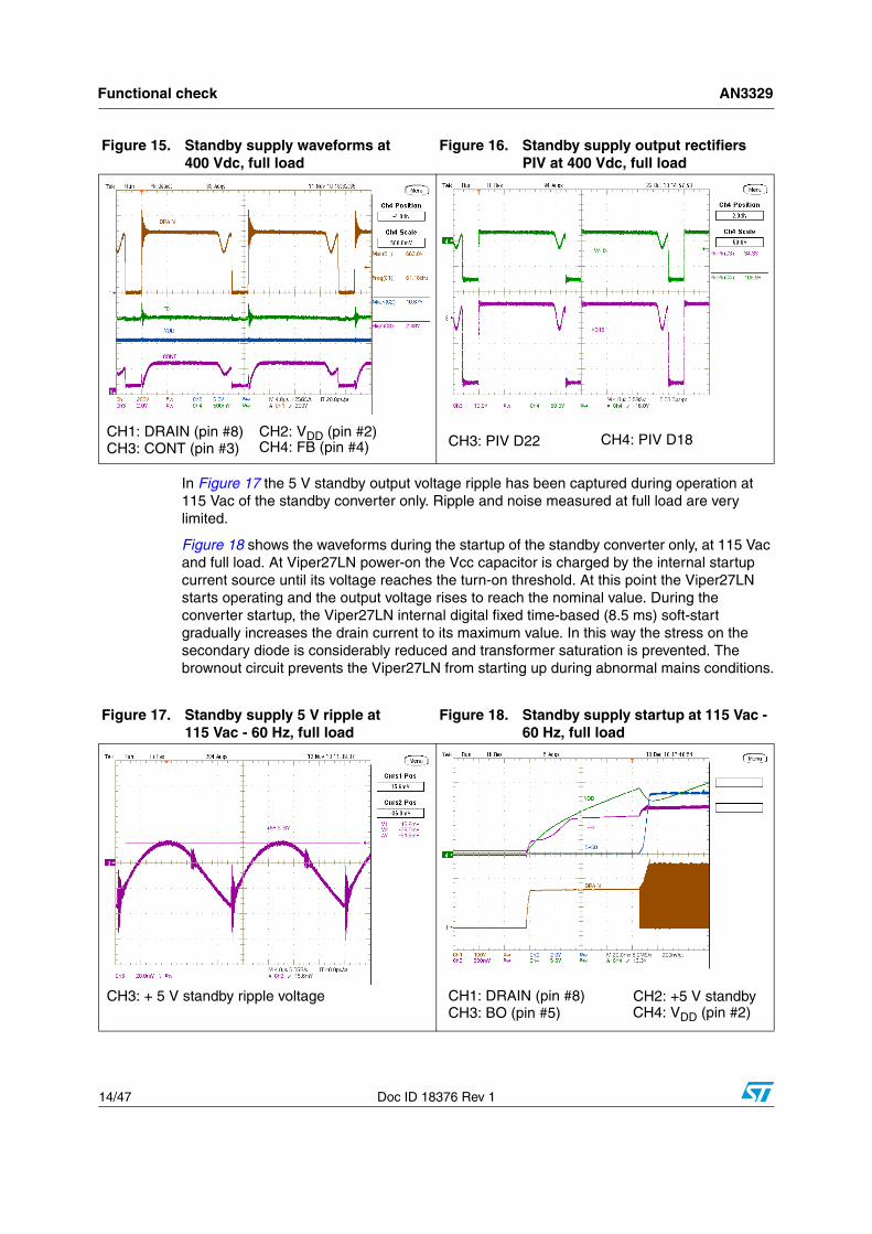
In Figure 15 the converter waveforms are captured while the PFC is working and the standby supply is powered with 400 V. The margin with respect to the Viper27LN maximum drain voltage can be noted on the sidebar on the right.
In Figure 16 typical waveforms relevant to the secondary side have been captured; the maximum reverse voltages applied to the rectifier at 400 V during full load operation with PFC working are, even in this case, well below the component's maximum ratings, ensuring long term reliability.
Figure 13. Standby supply waveforms at 115 Vac - 60 Hz, full load
Figure 14. Standby supply waveforms at 230 Vac - 50 Hz, full load
CH1: DRAIN (pin #8)CH3: CONT (pin #3)
CH2: VDD (pin #2)CH4: FB (pin #4)
CH1: DRAIN (pin #8)CH3: CONT (pin #3)
CH2: VDD (pin #2)CH4: FB (pin #4)
Functional check AN3329
14/47 Doc ID 18376 Rev 1
In Figure 17 the 5 V standby output voltage ripple has been captured during operation at 115 Vac of the standby converter only. Ripple and noise measured at full load are very limited.
Figure 18 shows the waveforms during the startup of the standby converter only, at 115 Vac and full load. At Viper27LN power-on the Vcc capacitor is charged by the internal startup current source until its voltage reaches the turn-on threshold. At this point the Viper27LN starts operating and the output voltage rises to reach the nominal value. During the converter startup, the Viper27LN internal digital fixed time-based (8.5 ms) soft-start gradually increases the drain current to its maximum value. In this way the stress on the secondary diode is considerably reduced and transformer saturation is prevented. The brownout circuit prevents the Viper27LN from starting up during abnormal mains conditions.
Figure 15. Standby supply waveforms at 400 Vdc, full load
Figure 16. Standby supply output rectifiers PIV at 400 Vdc, full load
CH1: DRAIN (pin #8)CH3: CONT (pin #3)
CH2: VDD (pin #2)CH4: FB (pin #4) CH3: PIV D22 CH4: PIV D18
Figure 17. Standby supply 5 V ripple at 115 Vac - 60 Hz, full load
Figure 18. Standby supply startup at 115 Vac - 60 Hz, full load
CH3: + 5 V standby ripple voltage CH1: DRAIN (pin #8) CH2: +5 V standbyCH3: BO (pin #5) CH4: VDD (pin #2)
AN3329 Functional check
Doc ID 18376 Rev 1 15/47
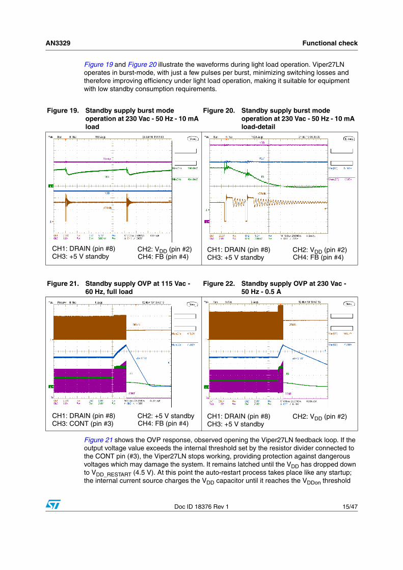
Figure 19 and Figure 20 illustrate the waveforms during light load operation. Viper27LN operates in burst-mode, with just a few pulses per burst, minimizing switching losses and therefore improving efficiency under light load operation, making it suitable for equipment with low standby consumption requirements.
Figure 21 shows the OVP response, observed opening the Viper27LN feedback loop. If the output voltage value exceeds the internal threshold set by the resistor divider connected to the CONT pin (#3), the Viper27LN stops working, providing protection against dangerous voltages which may damage the system. It remains latched until the VDD has dropped down to VDD_RESTART (4.5 V). At this point the auto-restart process takes place like any startup; the internal current source charges the VDD capacitor until it reaches the VDDon threshold
Figure 19. Standby supply burst mode operation at 230 Vac - 50 Hz - 10 mA load
Figure 20. Standby supply burst mode operation at 230 Vac - 50 Hz - 10 mA load-detail
CH1: DRAIN (pin #8) CH2: VDD (pin #2)CH3: +5 V standby CH4: FB (pin #4)
CH1: DRAIN (pin #8) CH2: VDD (pin #2)CH3: +5 V standby CH4: FB (pin #4)
Figure 21. Standby supply OVP at 115 Vac - 60 Hz, full load
Figure 22. Standby supply OVP at 230 Vac - 50 Hz - 0.5 A
CH1: DRAIN (pin #8) CH2: +5 V standbyCH3: CONT (pin #3) CH4: FB (pin #4)
CH1: DRAIN (pin #8) CH2: VDD (pin #2)CH3: +5 V standby
Functional check AN3329
16/47 Doc ID 18376 Rev 1
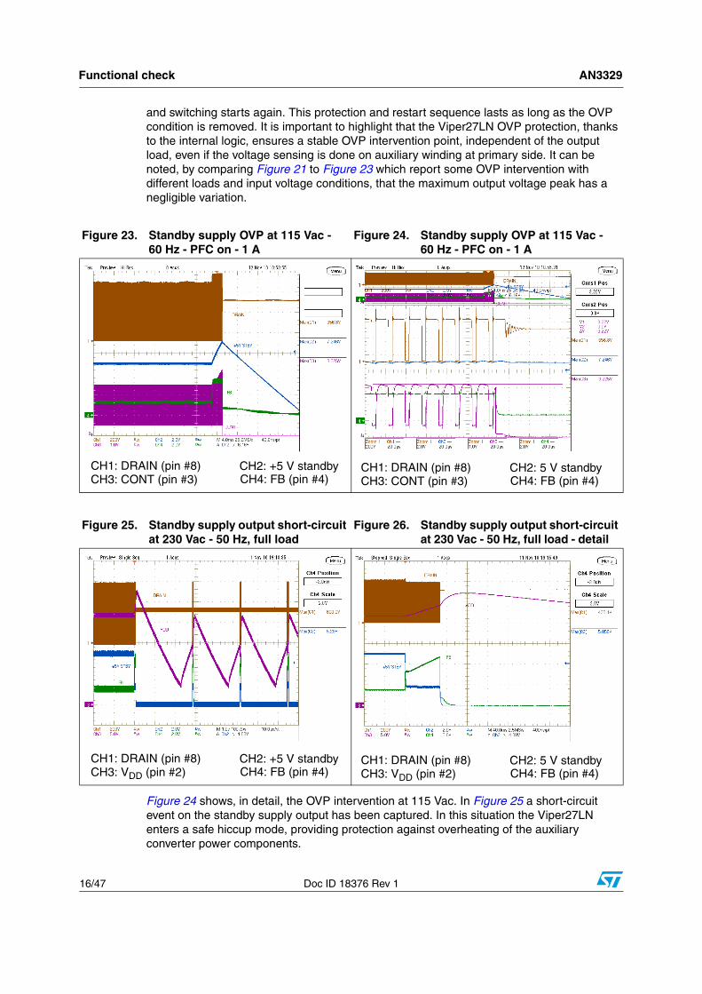
and switching starts again. This protection and restart sequence lasts as long as the OVP condition is removed. It is important to highlight that the Viper27LN OVP protection, thanks to the internal logic, ensures a stable OVP intervention point, independent of the output load, even if the voltage sensing is done on auxiliary winding at primary side. It can be noted, by comparing Figure 21 to Figure 23 which report some OVP intervention with different loads and input voltage conditions, that the maximum output voltage peak has a negligible variation.
Figure 24 shows, in detail, the OVP intervention at 115 Vac. In Figure 25 a short-circuit event on the standby supply output has been captured. In this situation the Viper27LN enters a safe hiccup mode, providing protection against overheating of the auxiliary converter power components.
Figure 23. Standby supply OVP at 115 Vac - 60 Hz - PFC on - 1 A
Figure 24. Standby supply OVP at 115 Vac - 60 Hz - PFC on - 1 A
CH1: DRAIN (pin #8) CH2: +5 V standbyCH3: CONT (pin #3) CH4: FB (pin #4)
CH1: DRAIN (pin #8) CH2: 5 V standbyCH3: CONT (pin #3) CH4: FB (pin #4)
Figure 25. Standby supply output short-circuit at 230 Vac - 50 Hz, full load
Figure 26. Standby supply output short-circuit at 230 Vac - 50 Hz, full load - detail
CH1: DRAIN (pin #8) CH2: +5 V standbyCH3: VDD (pin #2) CH4: FB (pin #4)
CH1: DRAIN (pin #8) CH2: 5 V standbyCH3: VDD (pin #2) CH4: FB (pin #4)
AN3329 Functional check
Doc ID 18376 Rev 1 17/47
In Figure 26 details of Viper27LN operation at short detection is captured; once an output short-circuit is detected, an internal current source charges the device internal circuitry and stops the auxiliary converter operation until the VDD voltage drops down to VDD_RESTART (4.5 V). At that time the internal HV current source is activated and charges the VDD capacitor until it reaches the VDDon threshold, then the Viper27LN restarts switching via a soft-start cycle. Hiccup cycles are repeated as long as the short-circuit condition lasts. Viper27LN is resumed back to normal operation only when the short-circuit condition is removed.
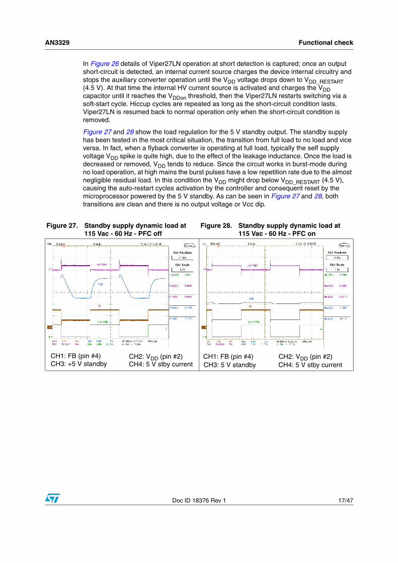
Figure 27 and 28 show the load regulation for the 5 V standby output. The standby supply has been tested in the most critical situation, the transition from full load to no load and vice versa. In fact, when a flyback converter is operating at full load, typically the self supply voltage VDD spike is quite high, due to the effect of the leakage inductance. Once the load is decreased or removed, VDD tends to reduce. Since the circuit works in burst-mode during no load operation, at high mains the burst pulses have a low repetition rate due to the almost negligible residual load. In this condition the VDD might drop below VDD_RESTART (4.5 V), causing the auto-restart cycles activation by the controller and consequent reset by the microprocessor powered by the 5 V standby. As can be seen in Figure 27 and 28, both transitions are clean and there is no output voltage or Vcc dip.
Figure 27. Standby supply dynamic load at 115 Vac - 60 Hz - PFC off
Figure 28. Standby supply dynamic load at 115 Vac - 60 Hz - PFC on
CH2: VDD (pin #2)CH3: +5 V standby CH4: 5 V stby currentCH1: FB (pin #4)
CH3: 5 V standbyCH1: FB (pin #4) CH2: VDD (pin #2)
CH4: 5 V stby current
Functional check AN3329
18/47 Doc ID 18376 Rev 1
Power factor corrector stage
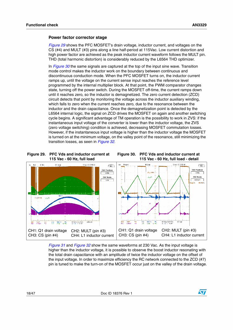
Figure 29 shows the PFC MOSFET's drain voltage, inductor current, and voltages on the CS (#4) and MULT (#3) pins along a line half-period at 115Vac. Low current distortion and high power factor are achieved as the peak inductor current waveform follows the MULT pin. THD (total harmonic distortion) is considerably reduced by the L6564 THD optimizer.
In Figure 30 the same signals are captured at the top of the input sine wave. Transition mode control makes the inductor work on the boundary between continuous and discontinuous conduction mode. When the PFC MOSFET turns on, the inductor current ramps up, until the voltage on the current sense input reaches the reference level programmed by the internal multiplier block. At that point, the PWM comparator changes state, turning off the power switch. During the MOSFET off-time, the current ramps down until it reaches zero, so the inductor is demagnetized. The zero current detection (ZCD) circuit detects that point by monitoring the voltage across the inductor auxiliary winding, which falls to zero when the current reaches zero, due to the resonance between the inductor and the drain capacitance. Once the demagnetization point is detected by the L6564 internal logic, the signal on ZCD drives the MOSFET on again and another switching cycle begins. A significant advantage of TM operation is the possibility to work in ZVS: if the instantaneous input voltage of the converter is lower than the inductor voltage, the ZVS (zero voltage switching) condition is achieved, decreasing MOSFET commutation losses. However, if the instantaneous input voltage is higher than the inductor voltage the MOSFET is turned on at the minimum voltage, on the valley point of the resonance, still minimizing the transition losses, as seen in Figure 32.
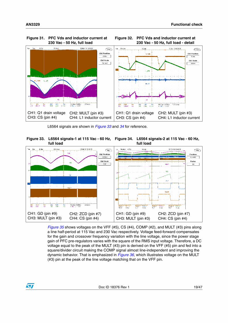
Figure 31 and Figure 32 show the same waveforms at 230 Vac. As the input voltage is higher than the inductor voltage, it is possible to observe the boost inductor resonating with the total drain capacitance with an amplitude of twice the inductor voltage on the offset of the input voltage. In order to maximize efficiency the RC network connected to the ZCD (#7) pin is tuned to make the turn-on of the MOSFET occur just on the valley of the drain voltage.
Figure 29. PFC Vds and inductor current at 115 Vac - 60 Hz, full load
Figure 30. PFC Vds and inductor current at 115 Vac - 60 Hz, full load - detail
CH2: MULT (pin #3)CH3: CS (pin #4) CH4: L1 inductor currentCH1: Q1 drain voltage
CH3: CS (pin #4)CH1: Q1 drain voltage CH2: MULT (pin #3)
CH4: L1 inductor current
AN3329 Functional check
Doc ID 18376 Rev 1 19/47
L6564 signals are shown in Figure 33 and 34 for reference.
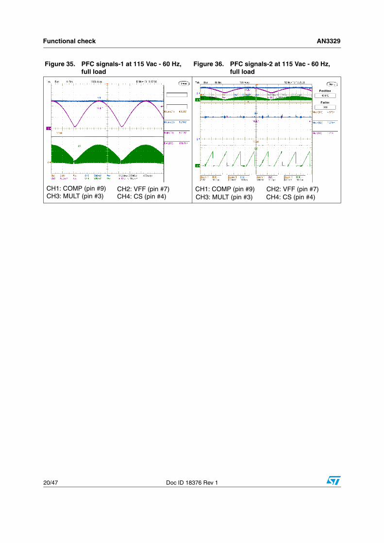
Figure 35 shows voltages on the VFF (#5), CS (#4), COMP (#2), and MULT (#3) pins along a line half-period at 115 Vac and 230 Vac respectively. Voltage feed-forward compensates for the gain and crossover frequency variation with the line voltage, since the power stage gain of PFC pre-regulators varies with the square of the RMS input voltage. Therefore, a DC voltage equal to the peak of the MULT (#3) pin is derived on the VFF (#5) pin and fed into a square/divider circuit making the COMP signal almost line-independent and improving the dynamic behavior. That is emphasized in Figure 36, which illustrates voltage on the MULT (#3) pin at the peak of the line voltage matching that on the VFF pin.
Figure 31. PFC Vds and inductor current at 230 Vac - 50 Hz, full load
Figure 32. PFC Vds and inductor current at 230 Vac - 50 Hz, full load - detail
CH2: MULT (pin #3)CH3: CS (pin #4) CH4: L1 inductor currentCH1: Q1 drain voltage
CH3: CS (pin #4)CH1: Q1 drain voltage CH2: MULT (pin #3)
CH4: L1 inductor current
Figure 33. L6564 signals-1 at 115 Vac - 60 Hz, full load
Figure 34. L6564 signals-2 at 115 Vac - 60 Hz, full load
CH2: ZCD (pin #7)CH3: MULT (pin #3) CH4: CS (pin #4)CH1: GD (pin #9)
CH3: MULT (pin #3)CH1: GD (pin #9) CH2: ZCD (pin #7)
CH4: CS (pin #4)
Functional check AN3329
20/47 Doc ID 18376 Rev 1
Figure 35. PFC signals-1 at 115 Vac - 60 Hz, full load
Figure 36. PFC signals-2 at 115 Vac - 60 Hz, full load
CH2: VFF (pin #7)CH3: MULT (pin #3) CH4: CS (pin #4)CH1: COMP (pin #9)
CH3: MULT (pin #3)CH1: COMP (pin #9) CH2: VFF (pin #7)
CH4: CS (pin #4)
AN3329 Functional check
Doc ID 18376 Rev 1 21/47
Resonant stage
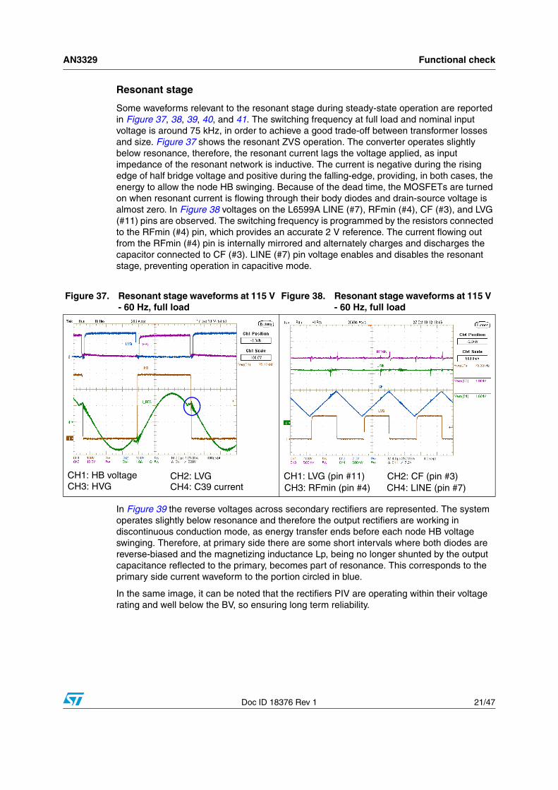
Some waveforms relevant to the resonant stage during steady-state operation are reported in Figure 37, 38, 39, 40, and 41. The switching frequency at full load and nominal input voltage is around 75 kHz, in order to achieve a good trade-off between transformer losses and size. Figure 37 shows the resonant ZVS operation. The converter operates slightly below resonance, therefore, the resonant current lags the voltage applied, as input impedance of the resonant network is inductive. The current is negative during the rising edge of half bridge voltage and positive during the falling-edge, providing, in both cases, the energy to allow the node HB swinging. Because of the dead time, the MOSFETs are turned on when resonant current is flowing through their body diodes and drain-source voltage is almost zero. In Figure 38 voltages on the L6599A LINE (#7), RFmin (#4), CF (#3), and LVG (#11) pins are observed. The switching frequency is programmed by the resistors connected to the RFmin (#4) pin, which provides an accurate 2 V reference. The current flowing out from the RFmin (#4) pin is internally mirrored and alternately charges and discharges the capacitor connected to CF (#3). LINE (#7) pin voltage enables and disables the resonant stage, preventing operation in capacitive mode.
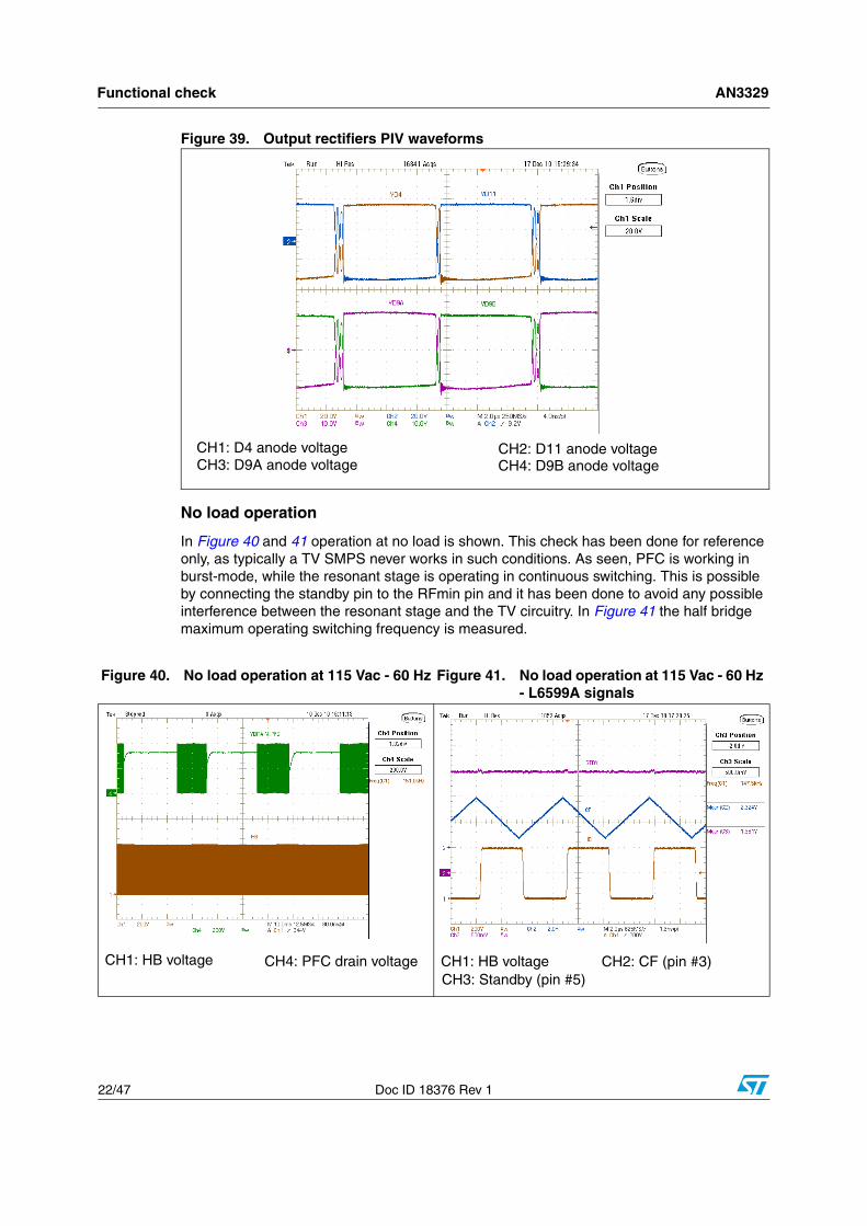
In Figure 39 the reverse voltages across secondary rectifiers are represented. The system operates slightly below resonance and therefore the output rectifiers are working in discontinuous conduction mode, as energy transfer ends before each node HB voltage swinging. Therefore, at primary side there are some short intervals where both diodes are reverse-biased and the magnetizing inductance Lp, being no longer shunted by the output capacitance reflected to the primary, becomes part of resonance. This corresponds to the primary side current waveform to the portion circled in blue.
In the same image, it can be noted that the rectifiers PIV are operating within their voltage rating and well below the BV, so ensuring long term reliability.
Figure 37. Resonant stage waveforms at 115 V - 60 Hz, full load
Figure 38. Resonant stage waveforms at 115 V - 60 Hz, full load
CH2: LVGCH3: HVG CH4: C39 currentCH1: HB voltage
CH3: RFmin (pin #4)CH1: LVG (pin #11) CH2: CF (pin #3)
CH4: LINE (pin #7)
Functional check AN3329
22/47 Doc ID 18376 Rev 1
Figure 39. Output rectifiers PIV waveforms
No load operation
In Figure 40 and 41 operation at no load is shown. This check has been done for reference only, as typically a TV SMPS never works in such conditions. As seen, PFC is working in burst-mode, while the resonant stage is operating in continuous switching. This is possible by connecting the standby pin to the RFmin pin and it has been done to avoid any possible interference between the resonant stage and the TV circuitry. In Figure 41 the half bridge maximum operating switching frequency is measured.
CH2: D11 anode voltageCH3: D9A anode voltage CH4: D9B anode voltageCH1: D4 anode voltage
Figure 40. No load operation at 115 Vac - 60 Hz Figure 41. No load operation at 115 Vac - 60 Hz - L6599A signals
CH4: PFC drain voltageCH1: HB voltageCH3: Standby (pin #5)CH1: HB voltage CH2: CF (pin #3)
AN3329 Functional check
Doc ID 18376 Rev 1 23/47
Dynamic load operation and output voltage regulation
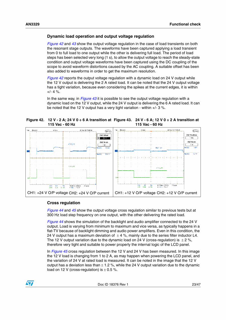
Figure 42 and 43 show the output voltage regulation in the case of load transients on both the resonant stage outputs. The waveforms have been captured applying a load transient from 0 to full load to one output while the other is delivering full load. The period of load steps has been selected very long (1 s), to allow the output voltage to reach the steady-state condition and output voltage waveforms have been captured using the DC coupling of the scope to avoid waveform distortions caused by the AC coupling. A suitable offset has been also added to waveforms in order to get the maximum resolution.
Figure 42 reports the output voltage regulation with a dynamic load on 24 V output while the 12 V output is delivering the 2 A rated load. It can be noted that the 24 V output voltage has a tight variation, because even considering the spikes at the current edges, it is within +/- 4 %.
In the same way, in Figure 43 it is possible to see the output voltage regulation with a dynamic load on the 12 V output, while the 24 V output is delivering the 6 A rated load. It can be noted that the 12 V output has a very tight variation - within +/- 3 %.
Cross regulation
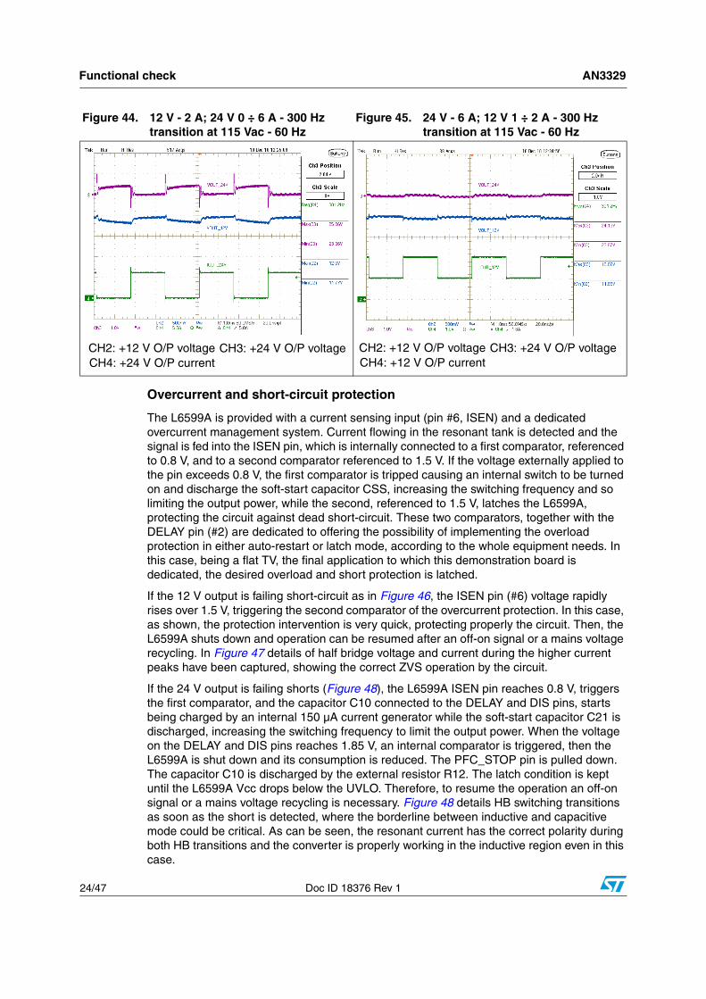
Figure 44 and 45 show the output voltage cross regulation similar to previous tests but at 300 Hz load step frequency on one output, with the other delivering the rated load.
Figure 44 shows the simulation of the backlight and audio amplifier connected to the 24 V output. Load is varying from minimum to maximum and vice versa, as typically happens in a flat-TV because of backlight dimming and audio power amplifiers. Even in this condition, the 24 V output has a maximum deviation of ± 4 %, mainly due to the series filter inductor L4. The 12 V output variation due to the dynamic load on 24 V (cross-regulation) is ± 2 %, therefore very tight and suitable to power properly the internal logic of the LCD panel.
In Figure 45 cross regulation between the 12 V and 24 V has been measured. In this image the 12 V load is changing from 1 to 2 A, as may happen when powering the LCD panel, and the variation of 24 V at rated load is measured. It can be noted in the image that the 12 V output has a deviation less than ± 1.2 %, while the 24 V output variation due to the dynamic load on 12 V (cross-regulation) is ± 0.5 %.
Figure 42. 12 V - 2 A; 24 V 0 ÷ 6 A transition at 115 Vac - 60 Hz
Figure 43. 24 V - 6 A; 12 V 0 ÷ 2 A transition at 115 Vac - 60 Hz
CH2: +24 V O/P currentCH1: +24 V O/P voltage CH1: +12 V O/P voltage CH2: +12 V O/P current
Functional check AN3329
24/47 Doc ID 18376 Rev 1
Overcurrent and short-circuit protection
The L6599A is provided with a current sensing input (pin #6, ISEN) and a dedicated overcurrent management system. Current flowing in the resonant tank is detected and the signal is fed into the ISEN pin, which is internally connected to a first comparator, referenced to 0.8 V, and to a second comparator referenced to 1.5 V. If the voltage externally applied to the pin exceeds 0.8 V, the first comparator is tripped causing an internal switch to be turned on and discharge the soft-start capacitor CSS, increasing the switching frequency and so limiting the output power, while the second, referenced to 1.5 V, latches the L6599A, protecting the circuit against dead short-circuit. These two comparators, together with the DELAY pin (#2) are dedicated to offering the possibility of implementing the overload protection in either auto-restart or latch mode, according to the whole equipment needs. In this case, being a flat TV, the final application to which this demonstration board is dedicated, the desired overload and short protection is latched.
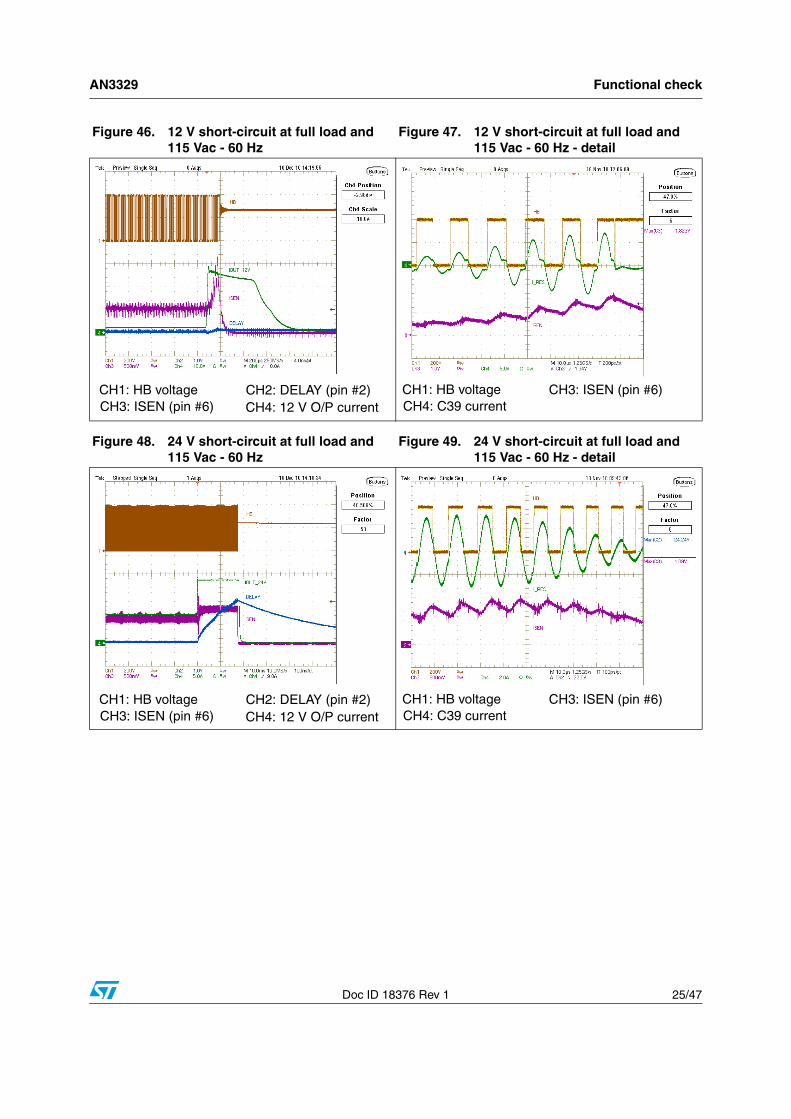
If the 12 V output is failing short-circuit as in Figure 46, the ISEN pin (#6) voltage rapidly rises over 1.5 V, triggering the second comparator of the overcurrent protection. In this case, as shown, the protection intervention is very quick, protecting properly the circuit. Then, the L6599A shuts down and operation can be resumed after an off-on signal or a mains voltage recycling. In Figure 47 details of half bridge voltage and current during the higher current peaks have been captured, showing the correct ZVS operation by the circuit.
If the 24 V output is failing shorts (Figure 48), the L6599A ISEN pin reaches 0.8 V, triggers the first comparator, and the capacitor C10 connected to the DELAY and DIS pins, starts being charged by an internal 150 µA current generator while the soft-start capacitor C21 is discharged, increasing the switching frequency to limit the output power. When the voltage on the DELAY and DIS pins reaches 1.85 V, an internal comparator is triggered, then the L6599A is shut down and its consumption is reduced. The PFC_STOP pin is pulled down. The capacitor C10 is discharged by the external resistor R12. The latch condition is kept until the L6599A Vcc drops below the UVLO. Therefore, to resume the operation an off-on signal or a mains voltage recycling is necessary. Figure 48 details HB switching transitions as soon as the short is detected, where the borderline between inductive and capacitive mode could be critical. As can be seen, the resonant current has the correct polarity during both HB transitions and the converter is properly working in the inductive region even in this case.
Figure 44. 12 V - 2 A; 24 V 0 ÷ 6 A - 300 Hz transition at 115 Vac - 60 Hz
Figure 45. 24 V - 6 A; 12 V 1 ÷ 2 A - 300 Hz transition at 115 Vac - 60 Hz
CH4: +24 V O/P currentCH2: +12 V O/P voltage CH3: +24 V O/P voltage
CH4: +12 V O/P currentCH2: +12 V O/P voltage CH3: +24 V O/P voltage
AN3329 Functional check
Doc ID 18376 Rev 1 25/47
Figure 46. 12 V short-circuit at full load and 115 Vac - 60 Hz
Figure 47. 12 V short-circuit at full load and 115 Vac - 60 Hz - detail
Figure 48. 24 V short-circuit at full load and 115 Vac - 60 Hz
Figure 49. 24 V short-circuit at full load and 115 Vac - 60 Hz - detail
CH3: ISEN (pin #6)CH1: HB voltage CH2: DELAY (pin #2)
CH4: 12 V O/P current CH4: C39 currentCH1: HB voltage CH3: ISEN (pin #6)
CH3: ISEN (pin #6)CH1: HB voltage CH2: DELAY (pin #2)
CH4: 12 V O/P current CH4: C39 currentCH1: HB voltage CH3: ISEN (pin #6)
Functional check AN3329
26/47 Doc ID 18376 Rev 1
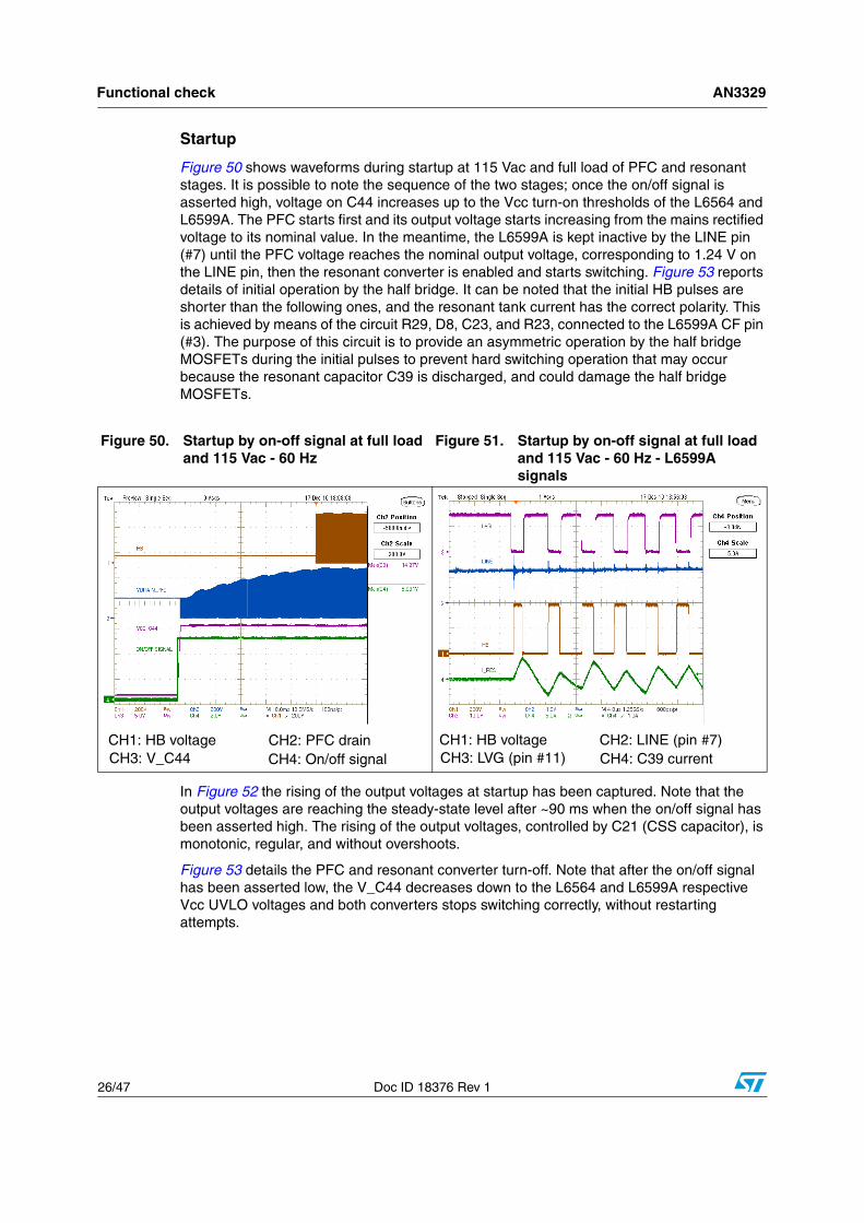
Startup
Figure 50 shows waveforms during startup at 115 Vac and full load of PFC and resonant stages. It is possible to note the sequence of the two stages; once the on/off signal is asserted high, voltage on C44 increases up to the Vcc turn-on thresholds of the L6564 and L6599A. The PFC starts first and its output voltage starts increasing from the mains rectified voltage to its nominal value. In the meantime, the L6599A is kept inactive by the LINE pin (#7) until the PFC voltage reaches the nominal output voltage, corresponding to 1.24 V on the LINE pin, then the resonant converter is enabled and starts switching. Figure 53 reports details of initial operation by the half bridge. It can be noted that the initial HB pulses are shorter than the following ones, and the resonant tank current has the correct polarity. This is achieved by means of the circuit R29, D8, C23, and R23, connected to the L6599A CF pin (#3). The purpose of this circuit is to provide an asymmetric operation by the half bridge MOSFETs during the initial pulses to prevent hard switching operation that may occur because the resonant capacitor C39 is discharged, and could damage the half bridge MOSFETs.
In Figure 52 the rising of the output voltages at startup has been captured. Note that the output voltages are reaching the steady-state level after ~90 ms when the on/off signal has been asserted high. The rising of the output voltages, controlled by C21 (CSS capacitor), is monotonic, regular, and without overshoots.
Figure 53 details the PFC and resonant converter turn-off. Note that after the on/off signal has been asserted low, the V_C44 decreases down to the L6564 and L6599A respective Vcc UVLO voltages and both converters stops switching correctly, without restarting attempts.
Figure 50. Startup by on-off signal at full load and 115 Vac - 60 Hz
Figure 51. Startup by on-off signal at full load and 115 Vac - 60 Hz - L6599A signals
CH3: V_C44CH1: HB voltage CH2: PFC drain
CH4: On/off signal CH3: LVG (pin #11)CH1: HB voltage CH2: LINE (pin #7)
CH4: C39 current
AN3329 Functional check
Doc ID 18376 Rev 1 27/47
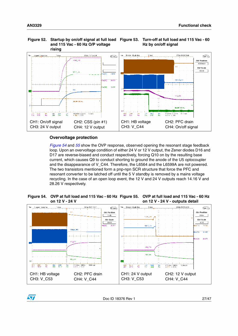
Overvoltage protection
Figure 54 and 55 show the OVP response, observed opening the resonant stage feedback loop. Upon an overvoltage condition of either 24 V or 12 V output, the Zener diodes D16 and D17 are reverse-biased and conduct respectively, forcing Q10 on by the resulting base current, which causes Q9 to conduct shorting to ground the anode of the U5 optocoupler and the disappearance of V_C44. Therefore, the L6564 and the L6599A are not powered. The two transistors mentioned form a pnp-npn SCR structure that force the PFC and resonant converter to be latched off until the 5 V standby is removed by a mains voltage recycling. In the case of an open loop event, the 12 V and 24 V outputs reach 14.16 V and 28.26 V respectively.
Figure 52. Startup by on/off signal at full load and 115 Vac - 60 Hz O/P voltage rising
Figure 53. Turn-off at full load and 115 Vac - 60 Hz by on/off signal
CH3: 24 V outputCH1: On/off signal CH2: CSS (pin #1)
CH4: 12 V output CH3: V_C44CH1: HB voltage CH2: PFC drain
CH4: On/off signal
Figure 54. OVP at full load and 115 Vac - 60 Hz on 12 V - 24 V
Figure 55. OVP at full load and 115 Vac - 60 Hz on 12 V - 24 V - outputs detail
CH3: V_C53CH1: HB voltage CH2: PFC drain
CH4: V_C44 CH3: V_C53CH1: 24 V output CH2: 12 V output
CH4: V_C44
Functional check AN3329
28/47 Doc ID 18376 Rev 1
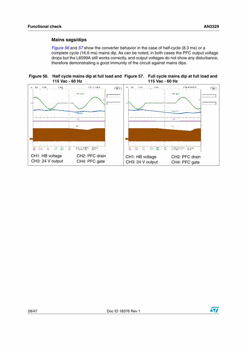
Mains sags/dips
Figure 56 and 57 show the converter behavior in the case of half-cycle (8.3 ms) or a complete cycle (16.6 ms) mains dip. As can be noted, in both cases the PFC output voltage drops but the L6599A still works correctly, and output voltages do not show any disturbance, therefore demonstrating a good immunity of the circuit against mains dips.
Figure 56. Half cycle mains dip at full load and 115 Vac - 60 Hz
Figure 57. Full cycle mains dip at full load and 115 Vac - 60 Hz
CH3: 24 V outputCH1: HB voltage CH2: PFC drain
CH4: PFC gate CH3: 24 V outputCH1: HB voltage CH2: PFC drain
CH4: PFC gate
AN3329 Conducted emission pre-compliance test
Doc ID 18376 Rev 1 29/47
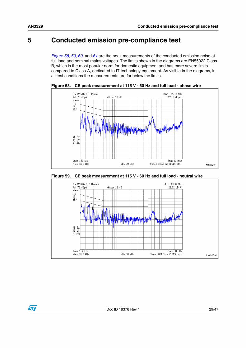
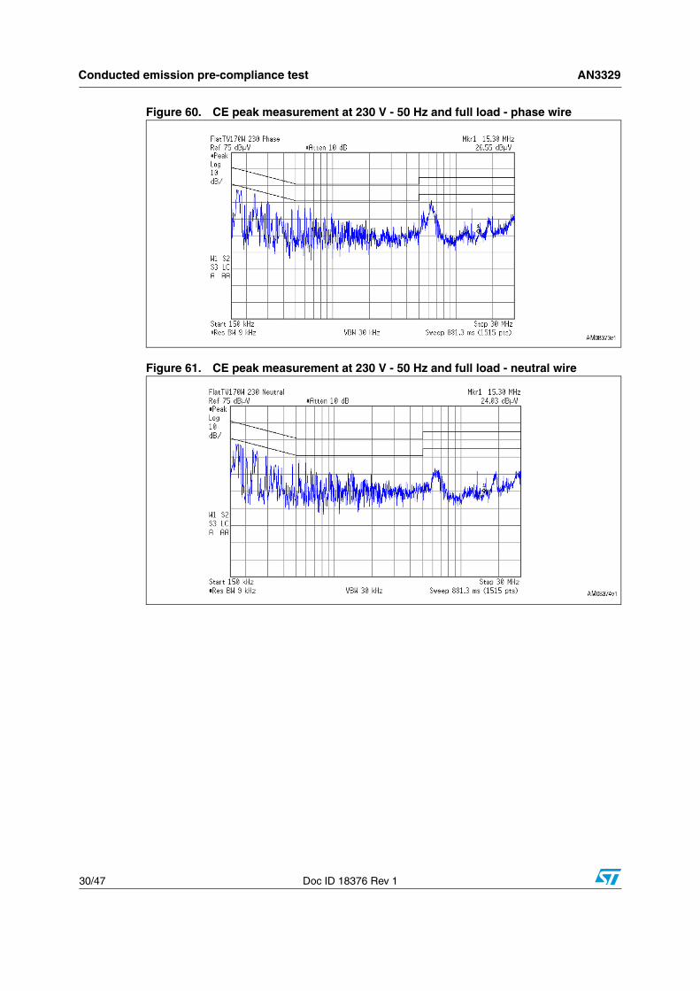
5 Conducted emission pre-compliance test
Figure 58, 59, 60, and 61 are the peak measurements of the conducted emission noise at full load and nominal mains voltages. The limits shown in the diagrams are EN55022 Class-B, which is the most popular norm for domestic equipment and has more severe limits compared to Class-A, dedicated to IT technology equipment. As visible in the diagrams, in all test conditions the measurements are far below the limits.
Figure 58. CE peak measurement at 115 V - 60 Hz and full load - phase wire
Figure 59. CE peak measurement at 115 V - 60 Hz and full load - neutral wire
Conducted emission pre-compliance test AN3329
30/47 Doc ID 18376 Rev 1
Figure 60. CE peak measurement at 230 V - 50 Hz and full load - phase wire
Figure 61. CE peak measurement at 230 V - 50 Hz and full load - neutral wire
AN3329 Bill of materials
Doc ID 18376 Rev 1 31/47
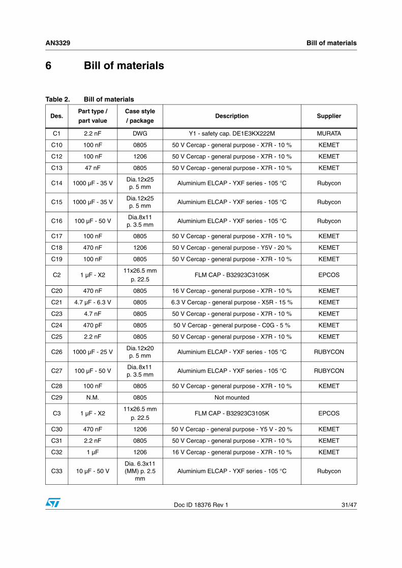
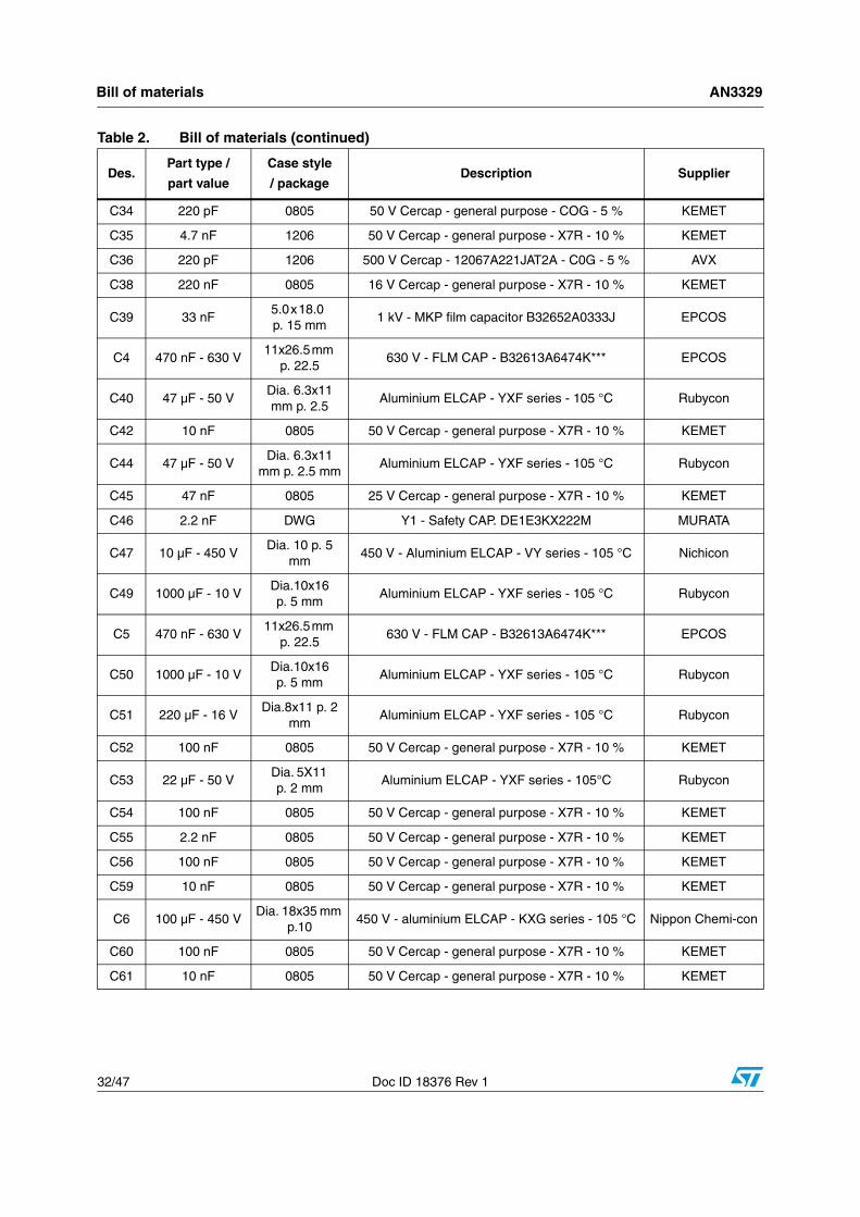
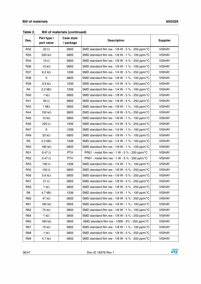
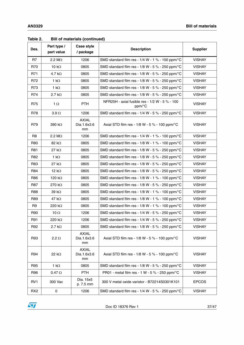
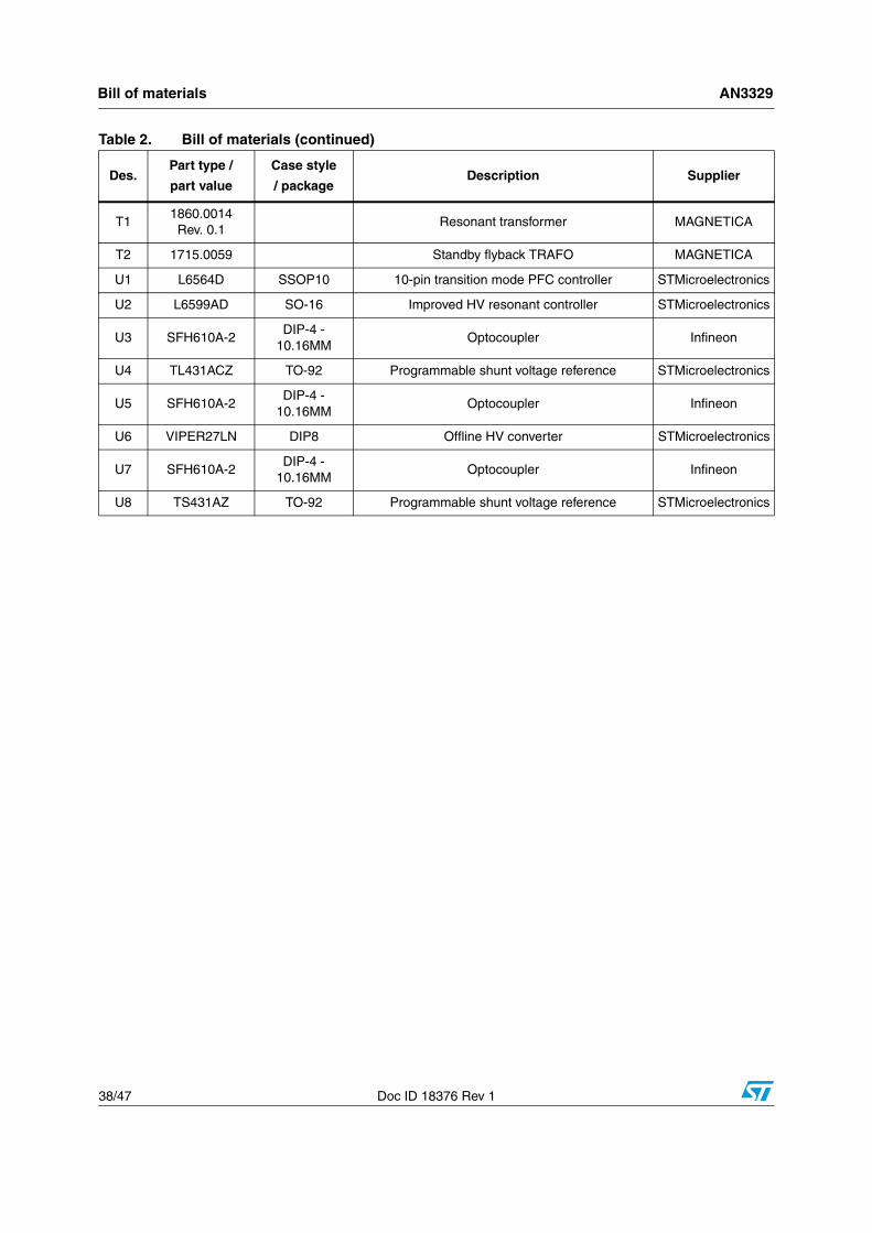
6 Bill of materials
Table 2. Bill of materials
Des.Part type /
part value
Case style
/ packageDescription Supplier
C1 2.2 nF DWG Y1 - safety cap. DE1E3KX222M MURATA
C10 100 nF 0805 50 V Cercap - general purpose - X7R - 10 % KEMET
C12 100 nF 1206 50 V Cercap - general purpose - X7R - 10 % KEMET
C13 47 nF 0805 50 V Cercap - general purpose - X7R - 10 % KEMET
C14 1000 µF - 35 VDia.12x25 p. 5 mm
Aluminium ELCAP - YXF series - 105 °C Rubycon
C15 1000 µF - 35 VDia.12x25 p. 5 mm
Aluminium ELCAP - YXF series - 105 °C Rubycon
C16 100 µF - 50 VDia.8x11 p. 3.5 mm
Aluminium ELCAP - YXF series - 105 °C Rubycon
C17 100 nF 0805 50 V Cercap - general purpose - X7R - 10 % KEMET
C18 470 nF 1206 50 V Cercap - general purpose - Y5V - 20 % KEMET
C19 100 nF 0805 50 V Cercap - general purpose - X7R - 10 % KEMET
C2 1 µF - X211x26.5 mm
p. 22.5FLM CAP - B32923C3105K EPCOS
C20 470 nF 0805 16 V Cercap - general purpose - X7R - 10 % KEMET
C21 4.7 µF - 6.3 V 0805 6.3 V Cercap - general purpose - X5R - 15 % KEMET
C23 4.7 nF 0805 50 V Cercap - general purpose - X7R - 10 % KEMET
C24 470 pF 0805 50 V Cercap - general purpose - C0G - 5 % KEMET
C25 2.2 nF 0805 50 V Cercap - general purpose - X7R - 10 % KEMET
C26 1000 µF - 25 VDia.12x20 p. 5 mm
Aluminium ELCAP - YXF series - 105 °C RUBYCON
C27 100 µF - 50 VDia. 8x11 p. 3.5 mm
Aluminium ELCAP - YXF series - 105 °C RUBYCON
C28 100 nF 0805 50 V Cercap - general purpose - X7R - 10 % KEMET
C29 N.M. 0805 Not mounted
C3 1 µF - X211x26.5 mm
p. 22.5FLM CAP - B32923C3105K EPCOS
C30 470 nF 1206 50 V Cercap - general purpose - Y5 V - 20 % KEMET
C31 2.2 nF 0805 50 V Cercap - general purpose - X7R - 10 % KEMET
C32 1 µF 1206 16 V Cercap - general purpose - X7R - 10 % KEMET
C33 10 µF - 50 VDia. 6.3x11 (MM) p. 2.5
mmAluminium ELCAP - YXF series - 105 °C Rubycon
Bill of materials AN3329
32/47 Doc ID 18376 Rev 1
C34 220 pF 0805 50 V Cercap - general purpose - COG - 5 % KEMET
C35 4.7 nF 1206 50 V Cercap - general purpose - X7R - 10 % KEMET
C36 220 pF 1206 500 V Cercap - 12067A221JAT2A - C0G - 5 % AVX
C38 220 nF 0805 16 V Cercap - general purpose - X7R - 10 % KEMET
C39 33 nF5.0 x 18.0 p. 15 mm
1 kV - MKP film capacitor B32652A0333J EPCOS
C4 470 nF - 630 V11x26.5 mm
p. 22.5630 V - FLM CAP - B32613A6474K*** EPCOS
C40 47 µF - 50 VDia. 6.3x11 mm p. 2.5
Aluminium ELCAP - YXF series - 105 °C Rubycon
C42 10 nF 0805 50 V Cercap - general purpose - X7R - 10 % KEMET
C44 47 µF - 50 VDia. 6.3x11
mm p. 2.5 mmAluminium ELCAP - YXF series - 105 °C Rubycon
C45 47 nF 0805 25 V Cercap - general purpose - X7R - 10 % KEMET
C46 2.2 nF DWG Y1 - Safety CAP. DE1E3KX222M MURATA
C47 10 µF - 450 VDia. 10 p. 5
mm450 V - Aluminium ELCAP - VY series - 105 °C Nichicon
C49 1000 µF - 10 VDia.10x16 p. 5 mm
Aluminium ELCAP - YXF series - 105 °C Rubycon
C5 470 nF - 630 V11x26.5 mm
p. 22.5630 V - FLM CAP - B32613A6474K*** EPCOS
C50 1000 µF - 10 VDia.10x16 p. 5 mm
Aluminium ELCAP - YXF series - 105 °C Rubycon
C51 220 µF - 16 VDia.8x11 p. 2
mmAluminium ELCAP - YXF series - 105 °C Rubycon
C52 100 nF 0805 50 V Cercap - general purpose - X7R - 10 % KEMET
C53 22 µF - 50 VDia. 5X11 p. 2 mm
Aluminium ELCAP - YXF series - 105°C Rubycon
C54 100 nF 0805 50 V Cercap - general purpose - X7R - 10 % KEMET
C55 2.2 nF 0805 50 V Cercap - general purpose - X7R - 10 % KEMET
C56 100 nF 0805 50 V Cercap - general purpose - X7R - 10 % KEMET
C59 10 nF 0805 50 V Cercap - general purpose - X7R - 10 % KEMET
C6 100 µF - 450 VDia. 18x35 mm
p.10450 V - aluminium ELCAP - KXG series - 105 °C Nippon Chemi-con
C60 100 nF 0805 50 V Cercap - general purpose - X7R - 10 % KEMET
C61 10 nF 0805 50 V Cercap - general purpose - X7R - 10 % KEMET
Table 2. Bill of materials (continued)
Des.Part type /
part value
Case style
/ packageDescription Supplier
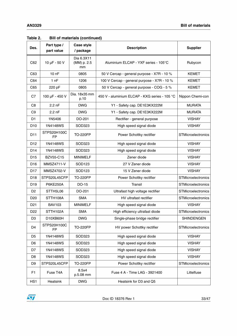
AN3329 Bill of materials
Doc ID 18376 Rev 1 33/47
C62 10 µF - 50 VDia 6.3X11 (MM) p. 2.5
mmAluminium ELCAP - YXF series - 105°C Rubycon
C63 10 nF 0805 50 V Cercap - general purpose - X7R - 10 % KEMET
C64 1 nF 1206 100 V Cercap - general purpose - X7R - 10 % KEMET
C65 220 pF 0805 50 V Cercap - general purpose - COG - 5 % KEMET
C7 100 µF - 450 VDia. 18x35 mm
p.10450 V - aluminium ELCAP - KXG series - 105 °C Nippon Chemi-con
C8 2.2 nF DWG Y1 - Safety cap. DE1E3KX222M MURATA
C9 2.2 nF DWG Y1 - Safety cap. DE1E3KX222M MURATA
D1 1N5406 DO-201 Rectifier - general purpose VISHAY
D10 1N4148WS SOD323 High speed signal diode VISHAY
D11STPS20H100C
FPTO-220FP Power Schottky rectifier STMicroelectronics
D12 1N4148WS SOD323 High speed signal diode VISHAY
D14 1N4148WS SOD323 High speed signal diode VISHAY
D15 BZV55-C15 MINIMELF Zener diode VISHAY
D16 MMSZ4711-V SOD123 27 V Zener diode VISHAY
D17 MMSZ4702-V SOD123 15 V Zener diode VISHAY
D18 STPS20L45CFP TO-220FP Power Schottky rectifier STMicroelectronics
D19 P6KE250A DO-15 Transil STMicroelectronics
D2 STTH5L06 DO-201 Ultrafast high voltage rectifier STMicroelectronics
D20 STTH108A SMA HV ultrafast rectifier STMicroelectronics
D21 BAV103 MINIMELF High speed signal diode VISHAY
D22 STTH102A SMA High efficiency ultrafast diode STMicroelectronics
D3 D10XB60H DWG Single-phase bridge rectifier SHINDENGEN
D4STPS20H100C
FPTO-220FP HV power Schottky rectifier STMicroelectronics
D5 1N4148WS SOD323 High speed signal diode VISHAY
D6 1N4148WS SOD323 High speed signal diode VISHAY
D7 1N4148WS SOD323 High speed signal diode VISHAY
D8 1N4148WS SOD323 High speed signal diode VISHAY
D9 STPS20L45CFP TO-220FP Power Schottky rectifier STMicroelectronics
F1 Fuse T4A8.5x4
p.5.08 mmFuse 4 A - Time LAG - 3921400 Littelfuse
HS1 Heatsink DWG Heatsink for D3 and Q5
Table 2. Bill of materials (continued)
Des.Part type /
part value
Case style
/ packageDescription Supplier
Bill of materials AN3329
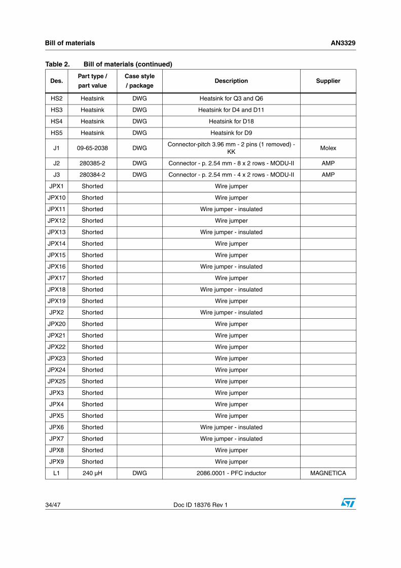
34/47 Doc ID 18376 Rev 1
HS2 Heatsink DWG Heatsink for Q3 and Q6
HS3 Heatsink DWG Heatsink for D4 and D11
HS4 Heatsink DWG Heatsink for D18
HS5 Heatsink DWG Heatsink for D9
J1 09-65-2038 DWGConnector-pitch 3.96 mm - 2 pins (1 removed) -
KKMolex
J2 280385-2 DWG Connector - p. 2.54 mm - 8 x 2 rows - MODU-II AMP
J3 280384-2 DWG Connector - p. 2.54 mm - 4 x 2 rows - MODU-II AMP
JPX1 Shorted Wire jumper
JPX10 Shorted Wire jumper
JPX11 Shorted Wire jumper - insulated
JPX12 Shorted Wire jumper
JPX13 Shorted Wire jumper - insulated
JPX14 Shorted Wire jumper
JPX15 Shorted Wire jumper
JPX16 Shorted Wire jumper - insulated
JPX17 Shorted Wire jumper
JPX18 Shorted Wire jumper - insulated
JPX19 Shorted Wire jumper
JPX2 Shorted Wire jumper - insulated
JPX20 Shorted Wire jumper
JPX21 Shorted Wire jumper
JPX22 Shorted Wire jumper
JPX23 Shorted Wire jumper
JPX24 Shorted Wire jumper
JPX25 Shorted Wire jumper
JPX3 Shorted Wire jumper
JPX4 Shorted Wire jumper
JPX5 Shorted Wire jumper
JPX6 Shorted Wire jumper - insulated
JPX7 Shorted Wire jumper - insulated
JPX8 Shorted Wire jumper
JPX9 Shorted Wire jumper
L1 240 µH DWG 2086.0001 - PFC inductor MAGNETICA
Table 2. Bill of materials (continued)
Des.Part type /
part value
Case style
/ packageDescription Supplier
AN3329 Bill of materials
Doc ID 18376 Rev 1 35/47
L2 3 mH DWG 1606.0007 EMI filter MAGNETICA
L3 70 µH 26x13 mm 2190.0001 DM inductor MAGNETICA
L4 2.2 µH DIA12 p. 5 mm 10610041 - 3 µH - 11 A inductor MAGNETICA
L5 1 µH DIA8 p. 5 mm 10710083 - 1 µ - 5 A inductor MAGNETICA
L6 1 µH DIA8 p. 5 mm 10710083 - 1 µ - 5 A inductor MAGNETICA
PCB PCB rev. 2 Single Layer - 2 OZ. - CEM-1
Q10 BC847C SOT-23 NPN small signal BJT VISHAY
Q11 BC847C SOT-23 NPN small signal BJT VISHAY
Q3 STF12NM50N TO-220FP N-channel Power MOSFET STMicroelectronics
Q5 STF14NM50N TO-220FP N-channel Power MOSFET STMicroelectronics
Q6 STF12NM50N TO-220FP N-channel Power MOSFET STMicroelectronics
Q7 BC847C SOT-23 NPN small signal BJT VISHAY
Q8 BC847C SOT-23 NPN small signal BJT VISHAY
Q9 BC857C SOT-23 PNP small signal BJT VISHAY
R1 NTC 2R5-S237 DWG NTC resistor P/N B57237S0259M000 EPCOS
R10 51 kΩ 0805 SMD standard film res - 1/8 W - 1 % - 100 ppm/°C VISHAY
R11 3.9 MΩ 1206 SMD standard film res - 1/4W - 1 % - 100 ppm/°C VISHAY
R12 470 kΩ 0805 SMD standard film res - 1/8 W - 5 % - 250 ppm/°C VISHAY
R13 130 kΩ 0805 SMD standard film res - 1/8 W - 5 % - 250 ppm/°C VISHAY
R15 2.2 MΩ 1206 SMD standard film res - 1/4 W - 1 % - 100 ppm/°C VISHAY
R16 3.9 MΩ 1206 SMD standard film res - 1/4 W - 1 % - 100 ppm/°C VISHAY
R17 200 kΩ 1206 SMD standard film res - 1/4 W - 1 % - 100 ppm/°C VISHAY
R18 56 Ω 0805 SMD standard film res - 1/8 W - 5 % - 250 ppm/°C VISHAY
R2 2.2 MΩ 1206 SMD standard film res - 1/4 W - 1 % - 100 ppm/°C VISHAY
R20 100 kΩ 0805 SMD standard film res - 1/8 W - 5 % - 250 ppm/°C VISHAY
R21 10 Ω 0805 SMD standard film res - 1/8 W - 5 % - 250 ppm/°C VISHAY
R22 3.9 kΩ 1206 SMD standard film res - 1/4 W - 5 % - 250 ppm/°C VISHAY
R23 4.7 MΩ 0805 SMD standard film res - 1/8 W - 5 % - 250 ppm/°C VISHAY
R24 3.3 kΩ 1206 SMD standard film res - 1/4 W - 5 % - 250 ppm/°C VISHAY
R25 10 Ω 0805 SMD standard film res - 1/8 W - 5 % - 250 ppm/°C VISHAY
R27 2.2 Ω 0805 SMD standard film res - 1/8 W - 5 % - 250 ppm/°C VISHAY
R29 4.7 kΩ 1206 SMD standard film res - 1/4 W - 5 % - 250 ppm/°C VISHAY
R3 27 kΩ 0805 SMD standard film res - 1/8 W - 1 % - 100 ppm/°C VISHAY
R31 100 kΩ 0805 SMD standard film res - 1/8 W - 5 % - 250 ppm/°C VISHAY
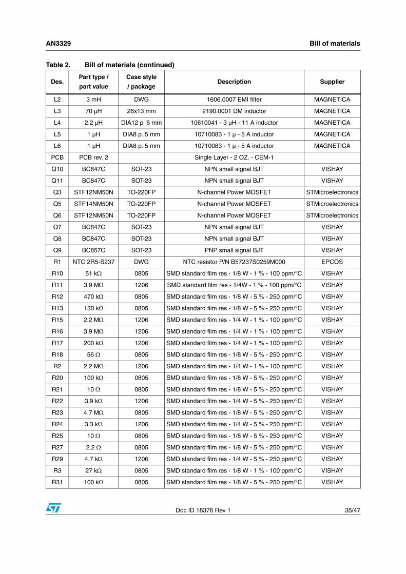
Table 2. Bill of materials (continued)
Des.Part type /
part value
Case style
/ packageDescription Supplier
Bill of materials AN3329
36/47 Doc ID 18376 Rev 1
R32 22 Ω 0805 SMD standard film res - 1/8 W - 5 % - 250 ppm/°C VISHAY
R33 200 kΩ 0805 SMD standard film res - 1/8 W - 1 % - 100 ppm/°C VISHAY
R34 10 Ω 0805 SMD standard film res - 1/8 W - 5 % - 250 ppm/°C VISHAY
R36 13 kΩ 0805 SMD standard film res - 1/8 W - 1 % - 100 ppm/°C VISHAY
R37 6.2 kΩ 1206 SMD standard film res - 1/4 W - 5 % - 250 ppm/°C VISHAY
R38 0 0805 SMD standard film res - 1/8 W - 1 % - 100 ppm/°C VISHAY
R39 3.9 kΩ 1206 SMD standard film res - 1/4 W - 5 % - 250 ppm/°C VISHAY
R4 2.2 MΩ 1206 SMD standard film res - 1/4 W - 1 % - 100 ppm/°C VISHAY
R40 1 kΩ 0805 SMD standard film res - 1/8 W - 5 % - 250 ppm/°C VISHAY
R41 56 Ω 0805 SMD standard film res - 1/8 W - 5 % - 250 ppm/°C VISHAY
R43 1 MΩ 0805 SMD standard film res - 1/8 W - 1 % - 100 ppm/°C VISHAY
R44 100 kΩ 0805 SMD standard film res - 1/8 W - 5 % - 250 ppm/°C VISHAY
R45 10 kΩ 0805 SMD standard film res - 1/8 W - 1 % - 100 ppm/°C VISHAY
R46 220 Ω 1206 SMD standard film res - 1/4 W - 5 % - 250 ppm/°C VISHAY
R47 0 1206 SMD standard film res - 1/4 W - 1 % - 100 ppm/°C VISHAY
R49 33 kΩ 0805 SMD standard film res - 1/8 W - 1 % - 100 ppm/°C VISHAY
R5 2.2 MΩ 1206 SMD standard film res - 1/4 W - 1 % - 100 ppm/°C VISHAY
R50 180 kΩ 0805 SMD standard film res - 1/8 W - 1 % - 100 ppm/°C VISHAY
R51 0.47 Ω PTH PR01 - metal film res - 1 W - 5 % - 250 ppm/°C VISHAY
R52 0.47 Ω PTH PR01 - metal film res - 1 W - 5 % - 250 ppm/°C VISHAY
R53 100 Ω 1206 SMD standard film res - 1/4 W - 1 % - 100 ppm/°C VISHAY
R55 150 Ω 0805 SMD standard film res - 1/8 W - 5 % - 250 ppm/°C VISHAY
R56 5.6 kΩ 0805 SMD standard film res - 1/8 W - 5 % - 250 ppm/°C VISHAY
R57 51 Ω 0805 SMD standard film res - 1/8 W - 5 % - 250 ppm/°C VISHAY
R59 1 kΩ 0805 SMD standard film res - 1/8 W - 5 % - 250 ppm/°C VISHAY
R6 4.7 MΩ 1206 SMD standard film res - 1/4 W - 1 % - 100 ppm/°C VISHAY
R60 47 kΩ 0805 SMD standard film res - 1/8 W - 5 % - 250 ppm/°C VISHAY
R61 180 kΩ 0805 SMD standard film res - 1/8 W - 1 % - 100 ppm/°C VISHAY
R62 75 kΩ 0805 SMD standard film res - 1/8 W - 1 % - 100 ppm/°C VISHAY
R64 1 kΩ 0805 SMD standard film res - 1/8 W - 5 % - 250 ppm/°C VISHAY
R65 180 kΩ 0805 SMD standard film res - 1/8W - 5% - 250 ppm/°C VISHAY
R67 10 kΩ 0805 SMD standard film res - 1/8 W - 1 % - 100 ppm/°C VISHAY
R68 1 kΩ 0805 SMD standard film res - 1/8 W - 5 % - 250 ppm/°C VISHAY
R69 4.7 kΩ 0805 SMD standard film res - 1/8 W - 5 % - 250 ppm/°C VISHAY
Table 2. Bill of materials (continued)
Des.Part type /
part value
Case style
/ packageDescription Supplier
AN3329 Bill of materials
Doc ID 18376 Rev 1 37/47
R7 2.2 MΩ 1206 SMD standard film res - 1/4 W - 1 % - 100 ppm/°C VISHAY
R70 10 kΩ 0805 SMD standard film res - 1/8 W - 5 % - 250 ppm/°C VISHAY
R71 4.7 kΩ 0805 SMD standard film res - 1/8 W - 5 % - 250 ppm/°C VISHAY
R72 1 kΩ 0805 SMD standard film res - 1/8 W - 5 % - 250 ppm/°C VISHAY
R73 1 kΩ 0805 SMD standard film res - 1/8 W - 5 % - 250 ppm/°C VISHAY
R74 2.7 kΩ 0805 SMD standard film res - 1/8 W - 5 % - 250 ppm/°C VISHAY
R75 1 Ω PTHNFR25H - axial fusible res - 1/2 W - 5 % - 100
ppm/°CVISHAY
R78 3.9 Ω 1206 SMD standard film res - 1/4 W - 5 % - 250 ppm/°C VISHAY
R79 390 kΩAXIAL
Dia.1.6x3.6 mm
Axial STD film res - 1/8 W - 5 % - 100 ppm/°C VISHAY
R8 2.2 MΩ 1206 SMD standard film res - 1/4 W - 1 % - 100 ppm/°C VISHAY
R80 82 kΩ 0805 SMD standard film res - 1/8 W - 1 % - 100 ppm/°C VISHAY
R81 27 kΩ 0805 SMD standard film res - 1/8 W - 5 % - 250 ppm/°C VISHAY
R82 1 kΩ 0805 SMD standard film res - 1/8 W - 5 % - 250 ppm/°C VISHAY
R83 27 kΩ 0805 SMD standard film res - 1/8 W - 5 % - 250 ppm/°C VISHAY
R84 12 kΩ 0805 SMD standard film res - 1/8 W - 5 % - 250 ppm/°C VISHAY
R86 120 kΩ 0805 SMD standard film res - 1/8 W - 1 % - 100 ppm/°C VISHAY
R87 270 kΩ 0805 SMD standard film res - 1/8 W - 5 % - 250 ppm/°C VISHAY
R88 39 kΩ 0805 SMD standard film res - 1/8 W - 1 % - 100 ppm/°C VISHAY
R89 47 kΩ 0805 SMD standard film res - 1/8 W - 1 % - 100 ppm/°C VISHAY
R9 220 kΩ 0805 SMD standard film res - 1/8 W - 1 % - 100 ppm/°C VISHAY
R90 10 Ω 1206 SMD standard film res - 1/4 W - 5 % - 250 ppm/°C VISHAY
R91 220 kΩ 1206 SMD standard film res - 1/4 W - 5 % - 250 ppm/°C VISHAY
R92 2.7 kΩ 0805 SMD standard film res - 1/8 W - 5 % - 250 ppm/°C VISHAY
R93 2.2 ΩAXIAL
Dia.1.6x3.6 mm
Axial STD film res - 1/8 W - 5 % - 100 ppm/°C VISHAY
R94 22 kΩAXIAL
Dia.1.6x3.6 mm
Axial STD film res - 1/8 W - 5 % - 100 ppm/°C VISHAY
R95 1 kΩ 0805 SMD standard film res - 1/8 W - 5 % - 250 ppm/°C VISHAY
R96 0.47 Ω PTH PR01 - metal film res - 1 W - 5 % - 250 ppm/°C VISHAY
RV1 300 VacDia. 15x5 p. 7.5 mm
300 V metal oxide varistor - B72214S0301K101 EPCOS
RX2 0 1206 SMD standard film res - 1/4 W - 5 % - 250 ppm/°C VISHAY
Table 2. Bill of materials (continued)
Des.Part type /
part value
Case style
/ packageDescription Supplier
Bill of materials AN3329
38/47 Doc ID 18376 Rev 1
T11860.0014 Rev. 0.1
Resonant transformer MAGNETICA
T2 1715.0059 Standby flyback TRAFO MAGNETICA
U1 L6564D SSOP10 10-pin transition mode PFC controller STMicroelectronics
U2 L6599AD SO-16 Improved HV resonant controller STMicroelectronics
U3 SFH610A-2DIP-4 -
10.16MMOptocoupler Infineon
U4 TL431ACZ TO-92 Programmable shunt voltage reference STMicroelectronics
U5 SFH610A-2DIP-4 -
10.16MMOptocoupler Infineon
U6 VIPER27LN DIP8 Offline HV converter STMicroelectronics
U7 SFH610A-2DIP-4 -
10.16MMOptocoupler Infineon
U8 TS431AZ TO-92 Programmable shunt voltage reference STMicroelectronics
Table 2. Bill of materials (continued)
Des.Part type /
part value
Case style
/ packageDescription Supplier
AN3329 PFC coil specifications
Doc ID 18376 Rev 1 39/47
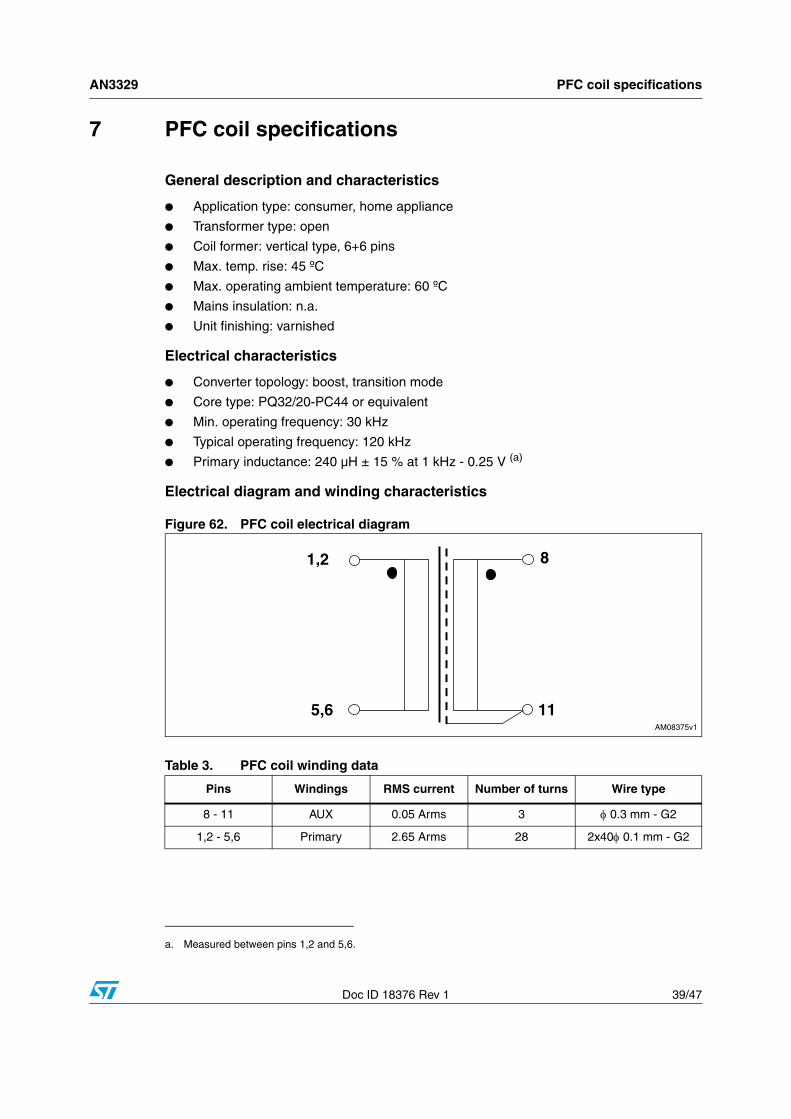
7 PFC coil specifications
General description and characteristics
● Application type: consumer, home appliance
● Transformer type: open
● Coil former: vertical type, 6+6 pins
● Max. temp. rise: 45 ºC
● Max. operating ambient temperature: 60 ºC
● Mains insulation: n.a.
● Unit finishing: varnished
Electrical characteristics
● Converter topology: boost, transition mode
● Core type: PQ32/20-PC44 or equivalent
● Min. operating frequency: 30 kHz
● Typical operating frequency: 120 kHz
● Primary inductance: 240 µH ± 15 % at 1 kHz - 0.25 V (a)
Electrical diagram and winding characteristics
Figure 62. PFC coil electrical diagram
a. Measured between pins 1,2 and 5,6.
Table 3. PFC coil winding data
Pins Windings RMS current Number of turns Wire type
8 - 11 AUX 0.05 Arms 3 φ 0.3 mm - G2
1,2 - 5,6 Primary 2.65 Arms 28 2x40φ 0.1 mm - G2
PFC coil specifications AN3329
40/47 Doc ID 18376 Rev 1
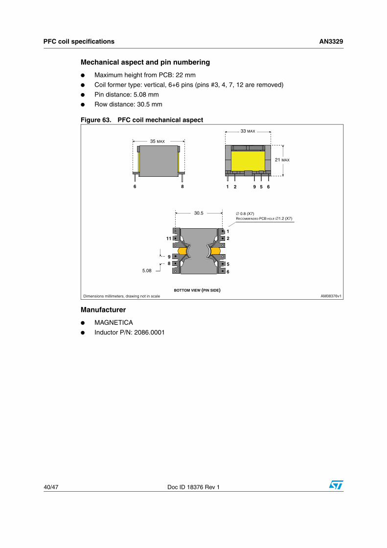
Mechanical aspect and pin numbering
● Maximum height from PCB: 22 mm
● Coil former type: vertical, 6+6 pins (pins #3, 4, 7, 12 are removed)
● Pin distance: 5.08 mm
● Row distance: 30.5 mm
Figure 63. PFC coil mechanical aspect
Manufacturer
● MAGNETICA
● Inductor P/N: 2086.0001
AM08376v1
BOTTOM VIEW (PIN SIDE)
∅ 0.8 (X7) RECOMMENDED PCB HOLE ∅1.2 (X7)
35 MAX
6 8 1 2 9 5 6
33 MAX
21 MAX
1
2
5
6
11
9 8
5.08
30.5
Dimensions millimeters, drawing not in scale
AN3329 Resonant power transformer specifications
Doc ID 18376 Rev 1 41/47
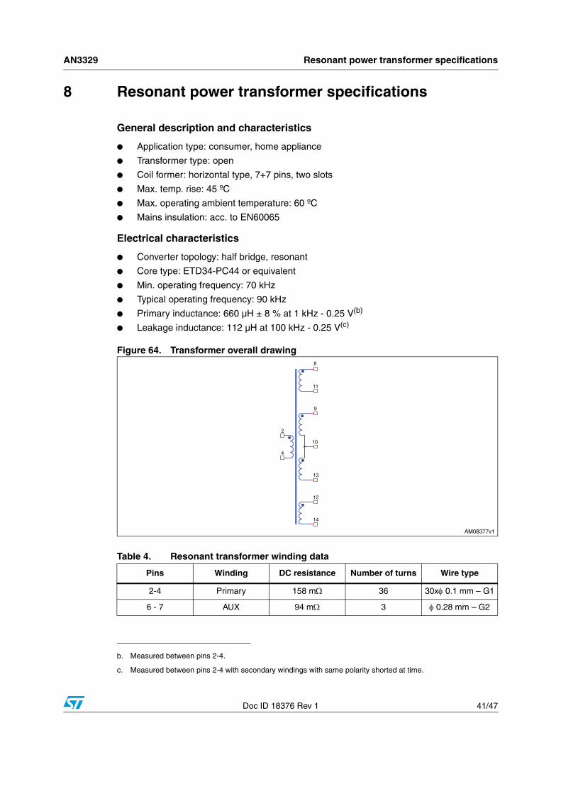
8 Resonant power transformer specifications
General description and characteristics
● Application type: consumer, home appliance
● Transformer type: open
● Coil former: horizontal type, 7+7 pins, two slots
● Max. temp. rise: 45 ºC
● Max. operating ambient temperature: 60 ºC
● Mains insulation: acc. to EN60065
Electrical characteristics
● Converter topology: half bridge, resonant
● Core type: ETD34-PC44 or equivalent
● Min. operating frequency: 70 kHz
● Typical operating frequency: 90 kHz
● Primary inductance: 660 µH ± 8 % at 1 kHz - 0.25 V(b)
● Leakage inductance: 112 µH at 100 kHz - 0.25 V(c)
Figure 64. Transformer overall drawing
b. Measured between pins 2-4.
c. Measured between pins 2-4 with secondary windings with same polarity shorted at time.
Table 4. Resonant transformer winding data
Pins Winding DC resistance Number of turns Wire type
2-4 Primary 158 mΩ 36 30xφ 0.1 mm – G1
6 - 7 AUX 94 mΩ 3 φ 0.28 mm – G2
Resonant power transformer specifications AN3329
42/47 Doc ID 18376 Rev 1
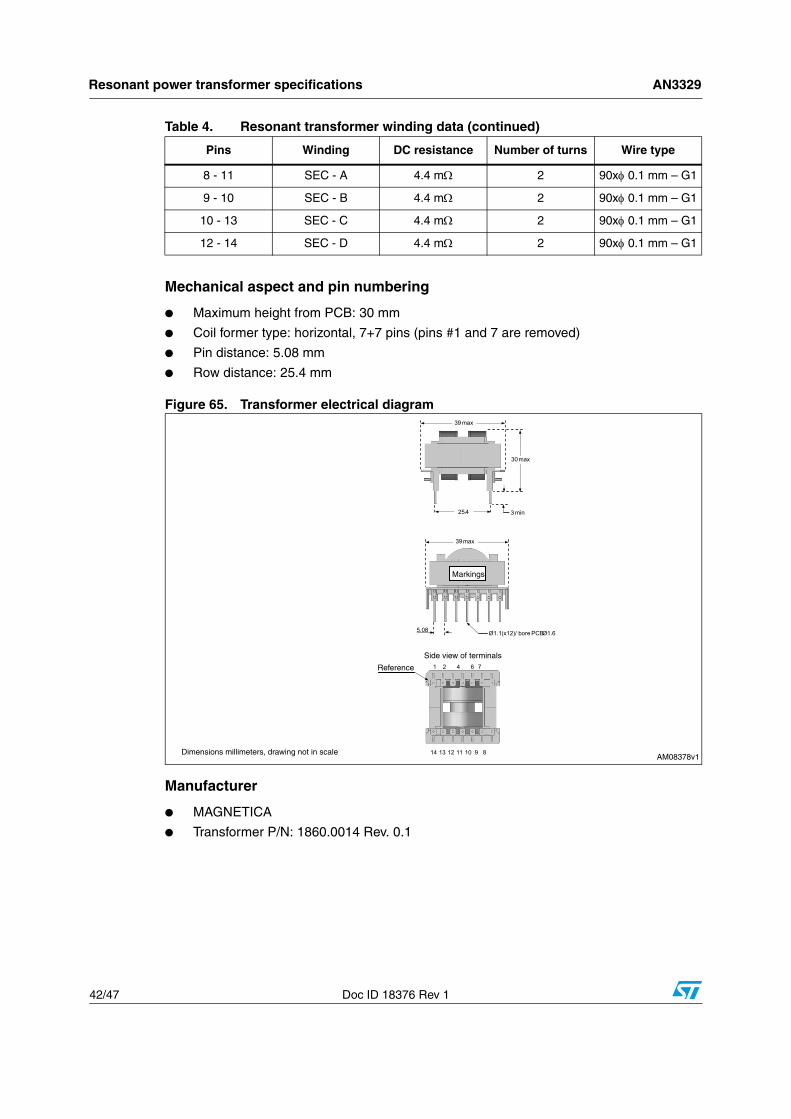
Mechanical aspect and pin numbering
● Maximum height from PCB: 30 mm
● Coil former type: horizontal, 7+7 pins (pins #1 and 7 are removed)
● Pin distance: 5.08 mm
● Row distance: 25.4 mm
Figure 65. Transformer electrical diagram
Manufacturer
● MAGNETICA
● Transformer P/N: 1860.0014 Rev. 0.1
8 - 11 SEC - A 4.4 mΩ 2 90xφ 0.1 mm – G1
9 - 10 SEC - B 4.4 mΩ 2 90xφ 0.1 mm – G1
10 - 13 SEC - C 4.4 mΩ 2 90xφ 0.1 mm – G1
12 - 14 SEC - D 4.4 mΩ 2 90xφ 0.1 mm – G1
Table 4. Resonant transformer winding data (continued)
Pins Winding DC resistance Number of turns Wire type
AN3329 Auxiliary flyback transformer specifications
Doc ID 18376 Rev 1 43/47
9 Auxiliary flyback transformer specifications
General description and characteristics
● Application type: consumer, home appliance
● Transformer type: open
● Winding type: layer
● Coil former: horizontal type, 4+5 pins, two slots
● Max. temp. rise: 45 ºC
● Max. operating ambient temperature: 60 ºC
● Mains insulation: acc. to EN60950
● Unit finishing: varnished
Electrical characteristics
● Converter topology: flyback, CCM/DCM mode
● Core type: E20-PC44 or equivalent
● Typical operating frequency: 60 kHz
● Primary inductance: 2.380 mH ± 10 % at 1 kHz - 0.25 V(d)
● Leakage inductance: 30 µH at 50 kHz - 0.25 V(e)
● Max. peak primary current: 0.5 Apk
● RMS primary current: 0.17 Arms
DC output characteristics
● Converter topology: flyback, CCM/DCM mode
d. Measured between pins 4-5.
e. Measured between pins 2-4 with secondary windings with same polarity shorted at time.
Table 5. DC output voltage and load
DC output voltage DC load
5 V 2 ADC
16 V 0.05 ADC
Auxiliary flyback transformer specifications AN3329
44/47 Doc ID 18376 Rev 1
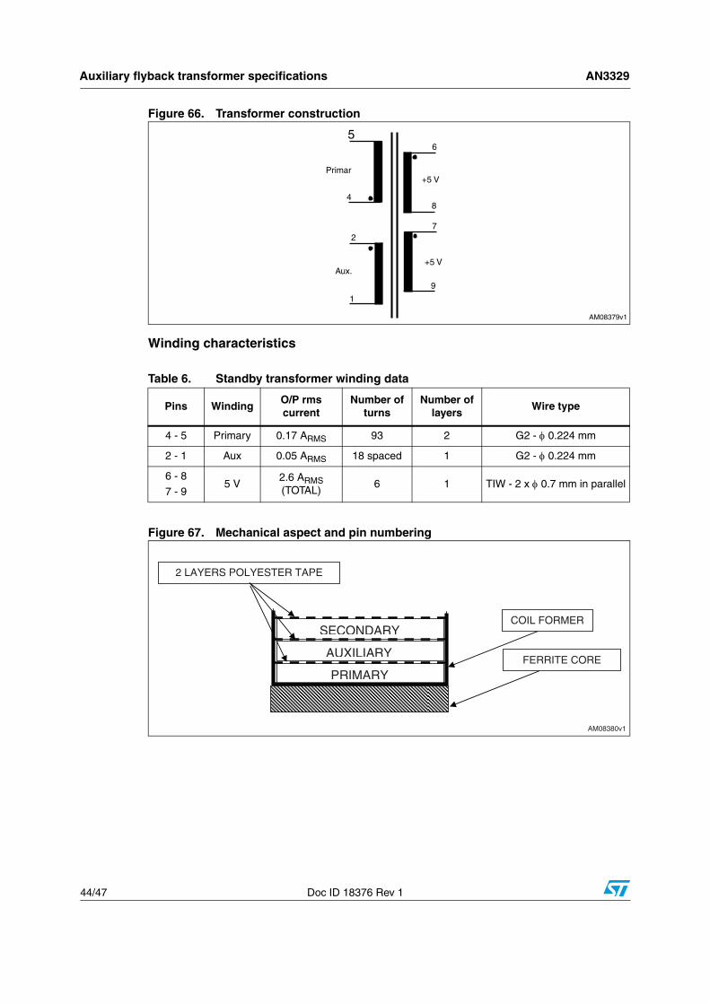
Figure 66. Transformer construction
Winding characteristics
Figure 67. Mechanical aspect and pin numbering
Table 6. Standby transformer winding data
Pins WindingO/P rms current
Number of turns
Number of layers
Wire type
4 - 5 Primary 0.17 ARMS 93 2 G2 - φ 0.224 mm
2 - 1 Aux 0.05 ARMS 18 spaced 1 G2 - φ 0.224 mm
6 - 8
7 - 95 V
2.6 ARMS (TOTAL)
6 1 TIW - 2 x φ 0.7 mm in parallel
AM08380v1
AUXILIARY
PRIMARY
SECONDARYCOIL FORMER
2 LAYERS POLYESTER TAPE
FERRITE CORE
AN3329 Auxiliary flyback transformer specifications
Doc ID 18376 Rev 1 45/47
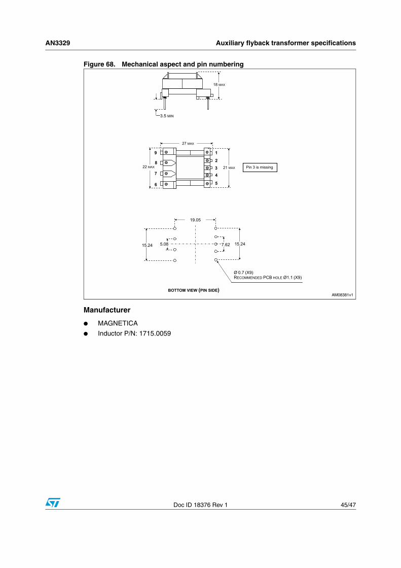
Figure 68. Mechanical aspect and pin numbering
Manufacturer
● MAGNETICA
● Inductor P/N: 1715.0059

Revision history AN3329
46/47 Doc ID 18376 Rev 1
10 Revision history
Table 7. Document revision history
Date Revision Changes
25-Feb-2011 1 Initial release.
AN3329
Doc ID 18376 Rev 1 47/47
Please Read Carefully:
Information in this document is provided solely in connection with ST products. STMicroelectronics NV and its subsidiaries (“ST”) reserve theright to make changes, corrections, modifications or improvements, to this document, and the products and services described herein at anytime, without notice.
All ST products are sold pursuant to ST’s terms and conditions of sale.
Purchasers are solely responsible for the choice, selection and use of the ST products and services described herein, and ST assumes noliability whatsoever relating to the choice, selection or use of the ST products and services described herein.
No license, express or implied, by estoppel or otherwise, to any intellectual property rights is granted under this document. If any part of thisdocument refers to any third party products or services it shall not be deemed a license grant by ST for the use of such third party productsor services, or any intellectual property contained therein or considered as a warranty covering the use in any manner whatsoever of suchthird party products or services or any intellectual property contained therein.
UNLESS OTHERWISE SET FORTH IN ST’S TERMS AND CONDITIONS OF SALE ST DISCLAIMS ANY EXPRESS OR IMPLIEDWARRANTY WITH RESPECT TO THE USE AND/OR SALE OF ST PRODUCTS INCLUDING WITHOUT LIMITATION IMPLIEDWARRANTIES OF MERCHANTABILITY, FITNESS FOR A PARTICULAR PURPOSE (AND THEIR EQUIVALENTS UNDER THE LAWSOF ANY JURISDICTION), OR INFRINGEMENT OF ANY PATENT, COPYRIGHT OR OTHER INTELLECTUAL PROPERTY RIGHT.
UNLESS EXPRESSLY APPROVED IN WRITING BY AN AUTHORIZED ST REPRESENTATIVE, ST PRODUCTS ARE NOTRECOMMENDED, AUTHORIZED OR WARRANTED FOR USE IN MILITARY, AIR CRAFT, SPACE, LIFE SAVING, OR LIFE SUSTAININGAPPLICATIONS, NOR IN PRODUCTS OR SYSTEMS WHERE FAILURE OR MALFUNCTION MAY RESULT IN PERSONAL INJURY,DEATH, OR SEVERE PROPERTY OR ENVIRONMENTAL DAMAGE. ST PRODUCTS WHICH ARE NOT SPECIFIED AS "AUTOMOTIVEGRADE" MAY ONLY BE USED IN AUTOMOTIVE APPLICATIONS AT USER’S OWN RISK.
Resale of ST products with provisions different from the statements and/or technical features set forth in this document shall immediately voidany warranty granted by ST for the ST product or service described herein and shall not create or extend in any manner whatsoever, anyliability of ST.
ST and the ST logo are trademarks or registered trademarks of ST in various countries.
Information in this document supersedes and replaces all information previously supplied.
The ST logo is a registered trademark of STMicroelectronics. All other names are the property of their respective owners.
© 2011 STMicroelectronics - All rights reserved
STMicroelectronics group of companies
Australia - Belgium - Brazil - Canada - China - Czech Republic - Finland - France - Germany - Hong Kong - India - Israel - Italy - Japan - Malaysia - Malta - Morocco - Philippines - Singapore - Spain - Sweden - Switzerland - United Kingdom - United States of America
www.st.com