Embed Size (px)
Citation preview
Deep Sub-100 nm Ge CMOS Devices on Si with the Recessed S/D and Channel Heng Wu, Wei Luo, Mengwei Si, Jingyun Zhang, Hong Zhou and Peide D. Ye*
School of Electrical and Computer Engineering, Purdue University, West Lafayette, IN 47906, U.S.A. *Tel: 1-765-494-7611, Fax: 1-765-496-6443, Email: [email protected]
Abstract We report on comprehensive studies of Ge CMOS devices
with the recessed channel and S/D fabricated on a Ge-on-insulator (GeOI) substrate. Both nFETs and pFETs with channel lengths (Lch) from 500 to 20 nm, channel thicknesses (Tch) from 90 to 15 nm, EOTs from 5 to 3 nm, and gate stacks with and without the post oxidation (PO) are investigated. Benefiting from the fully depleted ultra-thin body (FD-UTB) channel with a reasonable interface, a low sub-threshold slope (SS) of 95 mV/dec is obtained in a 60 nm Lch nFET and a record high ION/IOFF ratio of 106 is realized in a 300 nm Lch nFET. The recessed contact strongly dependents on the recessed depth and optimized recessed depth significantly improves the Ge contacts.
Introduction Ge is considered as a promising channel material in the post Si
CMOS era, due to its higher and near symmetrical carrier mobilities for both electrons and holes, large density of states, and Si-compatible low temperature process. Recently, many important progresses have been achieved [1-7]. In our previous report [8], a novel recessed channel and S/D technique is used to improve the Ge n-contact and the gate electrostatic control. In this paper, we carried out a comprehensive study of the device performance dependence on Lch, Tch, EOT and the interface passivation of both nFETs and pFETs with the recessed channel and S/D. The post oxidation process improves the Al2O3/GeOx/Ge interface. Determined by ion implantation profiles, the characteristics of nFETs are much more sensitive to Tch than those of pFETs. To better understand the temperature-dependent device OFF- and ON-state characteristics, the OFF-state band-to-band-tunneling (BTBT) generation rate and the ON-state injection velocity are simulated by TCAD.
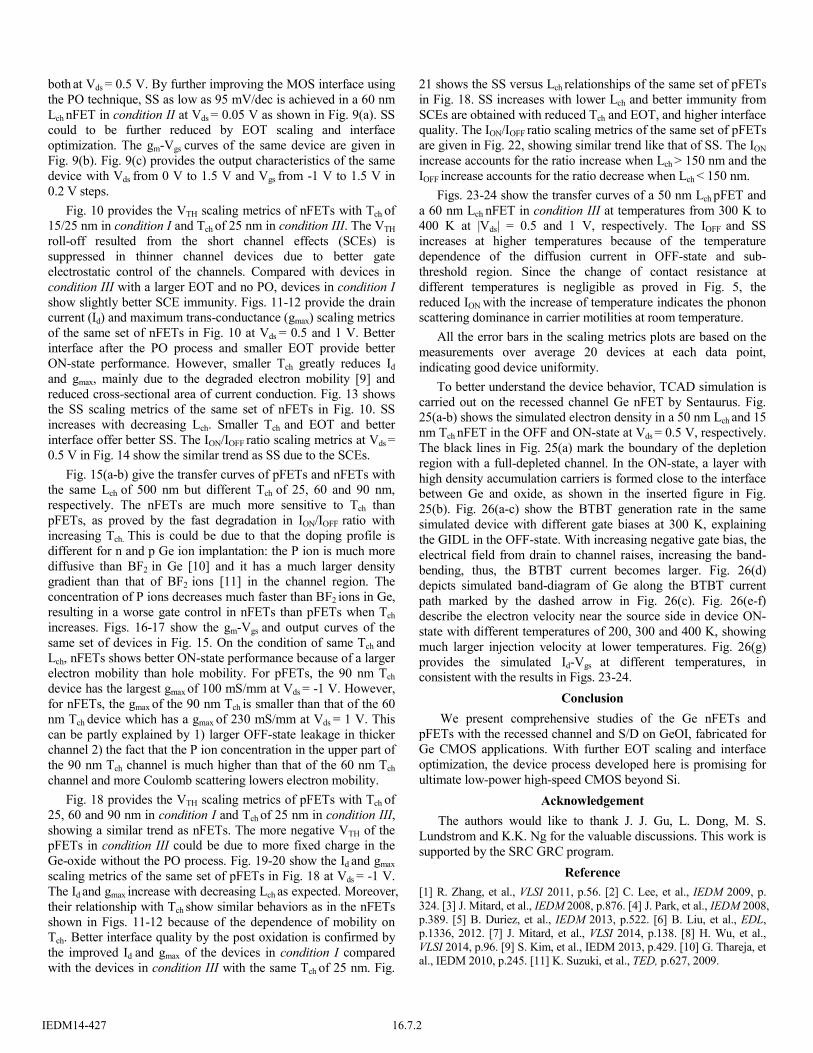
Experiment Fig. 1 shows the experiment process flows for both Ge nFETs
and pFETs. The device cross section at each main step is given in Fig. 2 and a brief summary on experimental splits is also included. The near-Gaussian distribution of the implanted ions in the Ge is plotted as the color-map shown in the cross section.
The starting material is a GeOI wafer with 180 nm lightly Sb-doped (100) Ge and 400 nm SiO2 on (100) Si from Soitec (step 1 in Fig. 2). An over-etched testing recess channel structure is given in Fig. 3, showing the layers of the substrate. The pFETs and nFETs were fabricated in parallel for better comparison. After cleaning and mesa isolation using SF6 based inductively coupled plasma (ICP) dry etching, ion implantation (step 2 in Fig. 2) was carried out for nFETs and pFETs using P and BF2 respectively, which were then separately activated by rapid thermal anneal (RTA) in different conditions. Then, the channel was formed by a SF6 ICP dry etching (step 3 in Fig. 2). For the recessed channels, depending on the etching time, Tch of 15, 25, 60 and 90 nm are realized, as shown in Fig. 3 (b-d). Next, the samples were
cyclically rinsed in 2% HF for 3 times as the surface wet clean. For the gate dielectrics, three conditions: 5 nm Al2O3 gate dielectric with the Ge post oxidation (PO) (condition I, EOT = 3 nm), 8 nm Al2O3 gate dielectric with the Ge PO (condition II, EOT = 4.5 nm) and 8 nm Al2O3 gate dielectric without the Ge PO (condition III, EOT = 5 nm), are studied. After the gate dielectric formation, the oxide in the S/D was first etched away and then a BCl3/Ar ICP dry etching was conducted to partially remove the top doped Ge layer as the recessed S/D etch. The etch rate is calibrated to be 15 nm/min. Determined by etching time, different recess depths were studied to optimize the quality of metal contacts on Ge, as shown in Fig. 4(a-b). Next, 100 nm Ni was deposited as the metal contacts for both nFETs and pFETs (step 4 in Fig. 2), followed by an Ohmic annealing by RTA. Finally, the gate metal was defined by 40/60 nm Ti/Au for the pFETs and 40/60 nm Ni/Au for the nFETs (step 5 in Fig. 2). All of the split conditions are applied to both nFETs and pFETs.
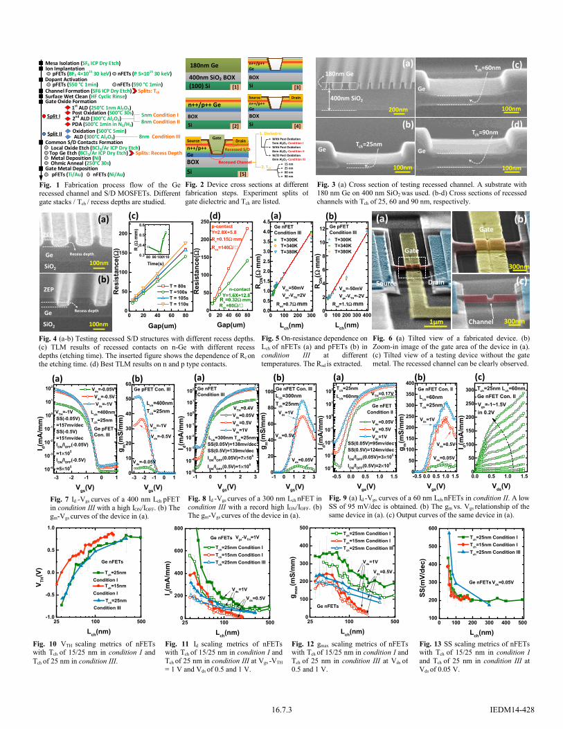
Results and Discussion Fig 4(c) shows the n-Ge TLM results with varying recess
etching time (recess depths). The inserted figure depicts the contact resistance (Rc) versus the etching time, demonstrating that Rc first decreases and then increases quickly with the etching time (recess depth). This is resulted from the near-Gaussian distribution profile of doping ions: with extended etching time, the doping concentration at the newly formed surface first increases and then decreases rapidly, hence, there is an optimized recess etching time or depth for low-resistivity Ohmic contacts on ion-implanted Ge. Fig. 5(a) shows the best TLM results, where the low Rc of 0.32 and 0.15 Ω·mm and sheet resistance (Rsh) of 80 and 140 Ω/ are achieved on n- and p-type Ge contacts, respectively. The difference of Rsh between n- and p-type contacts is mainly attributed to the difference of mobility between holes and electrons in Ge. Fig. 5(b-c) provide the ON-resistance (RON) versus Lch of pFETs and nFETs in condition III at |Vgs-VTH| = 2 V, |Vds| = 0.05 V at different temperatures. The source/drain series resistance (Rsd) is extracted to be 0.7 and 1.1 Ω·mm for nFETs and pFETs. Although the Rc of p-type Ge contact is smaller than that of n-type Ge contact, Rsd of pFETs is larger than that of nFETs because of a factor of 2 larger Rsh. The Rsd shows negligible dependence on temperature, indicating the dominance of the tunneling current in the Ohmic contacts.
Fig. 6(a) provides the titled SEM image of a fabricated device. The device gate area is enlarged in Fig. 6(b). The recessed channel can be clearly seen in the testing device without the gate metal in Fig. 6(c). Fig. 7(a) shows the transfer curves of a 400 nm Lch pFET in condition III at Vgs from 1 V to -3V and Vds = -0.05, -0.5 and -1 V. The device has a reasonable SS of 151 mV/dec and a high ION/IOFF ratio of 5×10⁵, both at Vds = -0.5 V. The gm-Vgs curves of the same device are given in Fig. 7(b). For comparison, a 300 nm Lch nFET in the same condition is given in Fig. 8, showing a decent SS of 139 mV/dec and a record high ION/IOFF ratio of 106,
16.7.1 IEDM14-426978-1-4799-8001-7/14/$31.00 ©2014 IEEE
both at Vds = 0.5 V. By further improving the MOS interface using the PO technique, SS as low as 95 mV/dec is achieved in a 60 nm Lch nFET in condition II at Vds = 0.05 V as shown in Fig. 9(a). SS could to be further reduced by EOT scaling and interface optimization. The gm-Vgs curves of the same device are given in Fig. 9(b). Fig. 9(c) provides the output characteristics of the same device with Vds from 0 V to 1.5 V and Vgs from -1 V to 1.5 V in 0.2 V steps.
Fig. 10 provides the VTH scaling metrics of nFETs with Tch of 15/25 nm in condition I and Tch of 25 nm in condition III. The VTH roll-off resulted from the short channel effects (SCEs) is suppressed in thinner channel devices due to better gate electrostatic control of the channels. Compared with devices in condition III with a larger EOT and no PO, devices in condition I show slightly better SCE immunity. Figs. 11-12 provide the drain current (Id) and maximum trans-conductance (gmax) scaling metrics of the same set of nFETs in Fig. 10 at Vds = 0.5 and 1 V. Better interface after the PO process and smaller EOT provide better ON-state performance. However, smaller Tch greatly reduces Id and gmax, mainly due to the degraded electron mobility [9] and reduced cross-sectional area of current conduction. Fig. 13 shows the SS scaling metrics of the same set of nFETs in Fig. 10. SS increases with decreasing Lch. Smaller Tch and EOT and better interface offer better SS. The ION/IOFF ratio scaling metrics at Vds = 0.5 V in Fig. 14 show the similar trend as SS due to the SCEs.
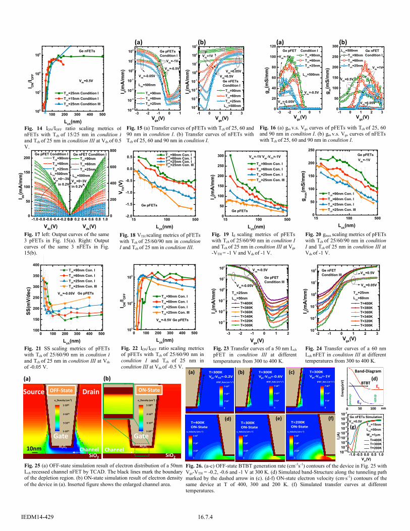
Fig. 15(a-b) give the transfer curves of pFETs and nFETs with the same Lch of 500 nm but different Tch of 25, 60 and 90 nm, respectively. The nFETs are much more sensitive to Tch than pFETs, as proved by the fast degradation in ION/IOFF ratio with increasing Tch. This is could be due to that the doping profile is different for n and p Ge ion implantation: the P ion is much more diffusive than BF2 in Ge [10] and it has a much larger density gradient than that of BF2 ions [11] in the channel region. The concentration of P ions decreases much faster than BF2 ions in Ge, resulting in a worse gate control in nFETs than pFETs when Tch increases. Figs. 16-17 show the gm-Vgs and output curves of the same set of devices in Fig. 15. On the condition of same Tch and Lch, nFETs shows better ON-state performance because of a larger electron mobility than hole mobility. For pFETs, the 90 nm Tch device has the largest gmax of 100 mS/mm at Vds = -1 V. However, for nFETs, the gmax of the 90 nm Tch is smaller than that of the 60 nm Tch device which has a gmax of 230 mS/mm at Vds = 1 V. This can be partly explained by 1) larger OFF-state leakage in thicker channel 2) the fact that the P ion concentration in the upper part of the 90 nm Tch channel is much higher than that of the 60 nm Tch channel and more Coulomb scattering lowers electron mobility.
Fig. 18 provides the VTH scaling metrics of pFETs with Tch of 25, 60 and 90 nm in condition I and Tch of 25 nm in condition III, showing a similar trend as nFETs. The more negative VTH of the pFETs in condition III could be due to more fixed charge in the Ge-oxide without the PO process. Fig. 19-20 show the Id and gmax scaling metrics of the same set of pFETs in Fig. 18 at Vds = -1 V. The Id and gmax increase with decreasing Lch as expected. Moreover, their relationship with Tch show similar behaviors as in the nFETs shown in Figs. 11-12 because of the dependence of mobility on Tch. Better interface quality by the post oxidation is confirmed by the improved Id and gmax of the devices in condition I compared with the devices in condition III with the same Tch of 25 nm. Fig.
21 shows the SS versus Lch relationships of the same set of pFETs in Fig. 18. SS increases with lower Lch and better immunity from SCEs are obtained with reduced Tch and EOT, and higher interface quality. The ION/IOFF ratio scaling metrics of the same set of pFETs are given in Fig. 22, showing similar trend like that of SS. The ION increase accounts for the ratio increase when Lch > 150 nm and the IOFF increase accounts for the ratio decrease when Lch < 150 nm.
Figs. 23-24 show the transfer curves of a 50 nm Lch pFET and a 60 nm Lch nFET in condition III at temperatures from 300 K to 400 K at |Vds| = 0.5 and 1 V, respectively. The IOFF and SS increases at higher temperatures because of the temperature dependence of the diffusion current in OFF-state and sub-threshold region. Since the change of contact resistance at different temperatures is negligible as proved in Fig. 5, the reduced ION with the increase of temperature indicates the phonon scattering dominance in carrier motilities at room temperature.
All the error bars in the scaling metrics plots are based on the measurements over average 20 devices at each data point, indicating good device uniformity.
To better understand the device behavior, TCAD simulation is carried out on the recessed channel Ge nFET by Sentaurus. Fig. 25(a-b) shows the simulated electron density in a 50 nm Lch and 15 nm Tch nFET in the OFF and ON-state at Vds = 0.5 V, respectively. The black lines in Fig. 25(a) mark the boundary of the depletion region with a full-depleted channel. In the ON-state, a layer with high density accumulation carriers is formed close to the interface between Ge and oxide, as shown in the inserted figure in Fig. 25(b). Fig. 26(a-c) show the BTBT generation rate in the same simulated device with different gate biases at 300 K, explaining the GIDL in the OFF-state. With increasing negative gate bias, the electrical field from drain to channel raises, increasing the band-bending, thus, the BTBT current becomes larger. Fig. 26(d) depicts simulated band-diagram of Ge along the BTBT current path marked by the dashed arrow in Fig. 26(c). Fig. 26(e-f) describe the electron velocity near the source side in device ON-state with different temperatures of 200, 300 and 400 K, showing much larger injection velocity at lower temperatures. Fig. 26(g) provides the simulated Id-Vgs at different temperatures, in consistent with the results in Figs. 23-24.
Conclusion We present comprehensive studies of the Ge nFETs and
pFETs with the recessed channel and S/D on GeOI, fabricated for Ge CMOS applications. With further EOT scaling and interface optimization, the device process developed here is promising for ultimate low-power high-speed CMOS beyond Si.
Acknowledgement The authors would like to thank J. J. Gu, L. Dong, M. S.
Lundstrom and K.K. Ng for the valuable discussions. This work is supported by the SRC GRC program.
Reference [1] R. Zhang, et al., VLSI 2011, p.56. [2] C. Lee, et al., IEDM 2009, p. 324. [3] J. Mitard, et al., IEDM 2008, p.876. [4] J. Park, et al., IEDM 2008, p.389. [5] B. Duriez, et al., IEDM 2013, p.522. [6] B. Liu, et al., EDL, p.1336, 2012. [7] J. Mitard, et al., VLSI 2014, p.138. [8] H. Wu, et al., VLSI 2014, p.96. [9] S. Kim, et al., IEDM 2013, p.429. [10] G. Thareja, et al., IEDM 2010, p.245. [11] K. Suzuki, et al., TED, p.627, 2009.
16.7.2IEDM14-427
Source DrainGate
n++/p++ Ge
BOX
Si
n++/p++ GeBOX
Si
n++/p++ Ge
BOX
Si
Source Drain
n++/p++ Ge
BOX
Si
400nm SiO2 BOX(100) Si
180nm Ge
Recessed Channel
Recessed S/D
2. Tch
1. Dielectric• With Post Oxidation
5nm Al2O3 -Condition I• With Post Oxidation
8nm Al2O3 -Condition II• W/O Post Oxidation
8nm Al2O3 -Condition III• 15 nm• 25 nm • 60 nm • 90 nm
[1]
[2]
[3]
[4]
[5]100nm
Ge
Tch=90nm
100nm
Ge
Tch=60nm
100nm
Tch=25nm
200nm
400nm SiO2
180nm Ge
Ge
(a)
(b)
(c)
(d)
25 100 500-1.0
-0.5
0.0
0.5
1.0
Tch=25nm Condition III
V TH(V
)
Lch(nm)
Tch=25nm Condition I
Tch=15nm Condition I
Ge nFETs
25 100 5000
100
200
300
400
500
Vds=1V
Ge nFETs
g max
(mS/
mm
)
Lch(nm)
Tch=25nm Condition I Tch=15nm Condition I Tch=25nm Condition III
Vds=0.5V
0 100 200 300 400 500100
200
300
400
500
600 Tch=25nm Condition I Tch=15nm Condition I Tch=25nm Condition III
SS(m
V/de
c)
Lch(nm)
Vds=0.05VGe nFETs
25 100 5000
200
400
600
800
Tch=25nm Condition I Tch=15nm Condition I Tch=25nm Condition III
Vds=0.5V
Vds=1V
Ge nFETs
I d(m
A/m
m)
Lch(nm)
Vgs-VTH=1V
Fig. 1 Fabrication process flow of the Gerecessed channel and S/D MOSFETs. Differentgate stacks / Tch / recess depths are studied.
Fig. 2 Device cross sections at differentfabrication steps. Experiment splits ofgate dielectric and Tch are listed.
Mesa Isolation (SF6 ICP Dry Etch)
Gate Oxide Formation
Metal Deposition (Ni)
Gate Metal Deposition
Channel Formation (SF6 ICP Dry Etch) Splits: Tch
Ion Implantation
Surface Wet Clean (HF Cyclic Rinse)
Common S/D Contacts FormationLocal Oxide Etch (BCl3/Ar ICP Dry Etch)
Top Ge Etch (BCl3/Ar ICP Dry Etch) Splits: Recess Depth
Ohmic Anneal (250°C 30s)
Dopant Activation
pFETs (Ti/Au) nFETs (Ni/Au)
pFETs (BF2 4×10¹⁵ 30 keV) nFETs (P 5×10¹⁵ 30 keV)
pFETs (550 °C 1min) nFETs (590 °C 1min)
1st ALD (250°C 1nm Al2O3)Post Oxidation (500°C 30s)
PDA (500°C 1min in N2/H2)
ALD (300°C Al2O3)Oxidation (500°C 5min)
Split I
Split II
5nm Condition I 8nm Condition II2nd ALD (300°C Al2O3)
8nm Condition III
Fig. 3 (a) Cross section of testing recessed channel. A substrate with 180 nm Ge on 400 nm SiO2 was used. (b-d) Cross sections of recessed channels with Tch of 25, 60 and 90 nm, respectively.
Fig. 9 (a) Id -Vgs curves of a 60 nm Lch nFETs in condition II. A low SS of 95 mV/dec is obtained. (b) The gm vs. Vgs relationship of the same device in (a). (c) Output curves of the same device in (a).
Fig. 7 Id -Vgs curves of a 400 nm Lch pFET in condition III with a high ION/IOFF. (b) The gm-Vgs curves of the device in (a).
Fig. 10 VTH scaling metrics of nFETs with Tch of 15/25 nm in condition I and Tch of 25 nm in condition III.
Fig. 11 Id scaling metrics of nFETswith Tch of 15/25 nm in condition I andTch of 25 nm in condition III at Vgs -VTH
= 1 V and Vds of 0.5 and 1 V.
Fig. 12 gmax scaling metrics of nFETswith Tch of 15/25 nm in condition I and Tch of 25 nm in condition III at Vds of 0.5 and 1 V.
Fig. 13 SS scaling metrics of nFETswith Tch of 15/25 nm in condition Iand Tch of 25 nm in condition III atVds of 0.05 V.
1µm
Source Drain
Gate
(a)
300nm
Gate(b)
300nmChannel
(c)
100nm
Recess depth
SiO2
Ge
100nm
Recess depth
SiO2
Ge
ZEP
ZEP
(a)
(b)
Fig. 4 (a-b) Testing recessed S/D structures with different recess depths.(c) TLM results of recessed contacts on n-Ge with different recessdepths (etching time). The inserted figure shows the dependence of Rc onthe etching time. (d) Best TLM results on n and p type contacts.
Fig. 5 On-resistance dependence on Lch of nFETs (a) and pFETs (b) in condition III at different temperatures. The Rsd is extracted.
Fig. 6 (a) Tilted view of a fabricated device. (b) Zoom-in image of the gate area of the device in (a). (c) Tilted view of a testing device without the gate metal. The recessed channel can be clearly observed.
-0.5 0.0 0.5 1.0 1.510-4
10-3
10-2
10-1
100
101
102
Ge nFET
Vds=0.05V Vds=0.5V Vds=1V
VTH=0.17V
Condition II
Tch=25nm Lch=60nm
SS(0.05V)=95mv/decSS(0.5V)=124mv/decION/IOFF(0.05V)=3×105
ION/IOFF(0.5V)=2×105
I d(mA
/mm
)
Vgs(V)-0.5 0.0 0.5 1.0 1.50
50
100
150
200
250
300
350
400
Vds=1V
Vds=0.5V
Vds=0.05V
Ge nFET Con. IILch=60nmTch=25nm
g m(m
S/m
m)
Vgs(V)0.0 0.5 1.0 1.50
50
100
150
200
250
300 Tch=25nm Lch=60nmGe nFET Con. II
I d(m
A/m
m)
Vds(V)
Vgs=-1~1.5Vin 0.2V
(a) (b) (c)
-1 0 1 2 30
20
40
60
80
100
Vds=0.5V
Vds=0.05V
Lch=300nmTch=25nm
Ge nFET Con. III
g m(m
S/m
m)
Vgs(V)
Vds=1V
-1 0 1 2 310-5
10-4
10-3
10-2
10-1
100
101
102
VTH=0.4V
Lch=300nm Tch=25nm
I d(mA
/mm
)
Vgs(V)
Vds=0.05V Vds=0.5V Vds=1V
Ge nFET Condition III
SS(0.05V)=138mv/decSS(0.5V)=139mv/decION/IOFF(0.05V)=7×105
ION/IOFF(0.5V)=1×106
(a) (b)
-3 -2 -1 0 110-4
10-3
10-2
10-1
100
101
102
Ge pFET Con. III
VTH=-1V SS(-0.05V)=157mv/decSS(-0.5V)=151mv/decION/IOFF(-0.05V)
=1×10⁵
ION/IOFF(-0.5V)
=5×10⁵
Vds=-0.05V Vds=-0.5V Vds=-1V
Lch=400nmTch=25nm
I d(m
A/m
m)
Vgs(V)-3 -2 -1 0 1
0
10
20
30
40
50
60
Vds=-1V
Vds=-0.5V
Vds=-0.05V
g m(m
S/m
m)
Vgs(V)
Lch=400nmTch=25nm
Ge pFET Con. III
(a) (b)
0 20 40 60 800
50
100
150
200
T = 80s T =100s T = 105s T = 110s
Res
ista
nce(
Ω)
Gap(um)
80 90 1001100.3
0.4
0.5
0.6
Rc(Ω
⋅mm
)
Time(s)
(c)
0 20 40 60 800
50
100
150
200
250
Rc=0.32Ω⋅mmRsh=80Ω/
p-contactY=2.8X+5.8Rc=0.15Ω⋅mm
Rsh=140Ω/
Res
ista
nce(
Ω)
Gap(um)
n-contactY=1.6X+12.8
(d)
0 100 200 3000.0
0.5
1.0
1.5
2.0
2.5
3.0
3.5
4.0
4.5
Rsd=0.7Ω⋅mm
T=300KT=340KT=380K
RO
N(Ω
⋅mm
)
Lch(nm)
Vds=50mVVgs-VTH=2V
Ge nFETCondition III
0 100 200 300 4000
2
4
6
8
10
12
RO
N(Ω
⋅mm
)Lch(nm)
Ge pFETCondition III
Rsd=1.1Ω⋅mm
Vds=-50mVVgs-VTH=-2V
T=300KT=340KT=380K
(a) (b)
Fig. 8 Id -Vgs curves of a 300 nm Lch nFET in condition III with a record high ION/IOFF. (b) The gm-Vgs curves of the device in (a).
16.7.3 IEDM14-428
100 200 300 400 500102
103
104
105
Tch=25nm Condition I Tch=15nm Condition I Tch=25nm Condition III
I ON/I O
FF
Lch(nm)
Ge nFETs
Vds=0.5V
-1 0 1 2 30
50
100
150
200
250
300Ge nFETCondition I
Vds=0.5V
Vds=1V
g m(m
S/m
m)
Vgs(V)
Vds=0.05V
Tch=90nmTch=60nmTch=25nm
Lch=500nm
-3 -2 -1 0 10
20
40
60
80
100
120
g m(m
S/m
m)
Ge pFET Condition I
Vds=-0.5V
Vds=-0.05V
Vds=-1V
Lch=500nm
Tch=90nm Tch=60nm Tch=25nm
Vgs(V)
(b)(a)
-1 0 1 2 310-4
10-3
10-2
10-1
100
101
102
103
Ge nFETsCondition I
Vds=0.5V
Vds=1V
Vds=0.05V
Lch=500nm
Tch=90nm Tch=60nm Tch=25nm
I d(m
A/m
m)
Vgs(V)-3 -2 -1 0 1
10-4
10-3
10-2
10-1
100
101
102 Ge pFETsCondition I
Lch=500nm
Tch=90nm Tch=60nm Tch=25nm
Vds=-1V
Vds=-0.5V
I d(mA
/mm
)Vgs(V)
Vds=-0.05V
(b)(a)
15 100 5000
50
100
150
200
250
g max
(mS/
mm
)
Lch(nm)
Tch=90nm Con. I Tch=60nm Con. I Tch=25nm Con. I Tch=25nm Con. III
Vds=-1VGe pFETs
15 100 500-2.0
-1.5
-1.0
-0.5
0.0
0.5 Tch=25nm Con. I Tch=60nm Con. I Tch=90nm Con. I
Tch=25nm Con. III
V TH(V
)
Lch(nm)
Ge pFETs
15 100 5000
50
100
150
200
250
300
Ge pFETs
Tch=90nm Con. I Tch=60nm Con. I Tch=25nm Con. I Tch=25nm Con. III
I d(m
A/m
m)
Lch(nm)
Vds=-1V Vgs-VTH=-1V
-1.0 -0.8 -0.6 -0.4 -0.2 0.00
50
100
150
200
I ds(m
A/m
m)
Ge pFET Condition I Tch=90nm Tch=60nm Tch=25nm
Vds(V)
Vgs=0~-3V in 0.2V
Lch=500nm
0.0 0.2 0.4 0.6 0.8 1.00
200
400
600
800
Tch=90nm Tch=60nm Tch=25nm
Vds(V)
Vgs=0~3Vin 0.2V
Lch=500nm
Ge nFET Condition I
Fig. 14 ION/IOFF ratio scaling metrics ofnFETs with Tch of 15/25 nm in condition Iand Tch of 25 nm in condition III at Vds of 0.5V.
Fig. 15 (a) Transfer curves of pFETs with Tch of 25, 60 and90 nm in condition I. (b) Transfer curves of nFETs withTch of 25, 60 and 90 nm in condition I.
Fig. 16 (a) gm v.s. Vgs curves of pFETs with Tch of 25, 60 and 90 nm in condition I. (b) gm v.s. Vgs curves of nFETs with Tch of 25, 60 and 90 nm in condition I.
Fig. 17 left: Output curves of the same3 pFETs in Fig. 15(a). Right: Outputcurves of the same 3 nFETs in Fig.15(b).
Fig. 18 VTH scaling metrics of pFETswith Tch of 25/60/90 nm in condition I and Tch of 25 nm in condition III.
Fig. 19 Id scaling metrics of pFETs with Tch of 25/60/90 nm in condition Iand Tch of 25 nm in condition III at Vgs -VTH = -1 V and Vds of -1 V.
Fig. 20 gmax scaling metrics of pFETswith Tch of 25/60/90 nm in conditionI and Tch of 25 nm in condition III atVds of -1 V.
Fig. 21 SS scaling metrics of pFETswith Tch of 25/60/90 nm in condition Iand Tch of 25 nm in condition III at Vdsof -0.05 V.
Fig. 22 ION/IOFF ratio scaling metricsof pFETs with Tch of 25/60/90 nm incondition I and Tch of 25 nm incondition III at Vds of -0.5 V.
Fig. 23 Transfer curves of a 50 nm Lch
pFET in condition III at differenttemperatures from 300 to 400 K.
Fig. 24 Transfer curves of a 60 nmLch nFET in condition III at differenttemperatures from 300 to 400 K.
Fig. 25 (a) OFF-state simulation result of electron distribution of a 50nmLch recessed channel nFET by TCAD. The black lines mark the boundaryof the depletion region. (b) ON-state simulation result of electron densityof the device in (a). Inserted figure shows the enlarged channel area.
Fig. 26. (a-c) OFF-state BTBT generation rate (cm-3s-1) contours of the device in Fig. 25 withVgs-VTH = -0.2, -0.6 and -1 V at 300 K. (d) Simulated band-Structure along the tunneling pathmarked by the dashed arrow in (c). (d-f) ON-state electron velocity (cm·s-1) contours of thesame device at T of 400, 300 and 200 K. (f) Simulated transfer curves at differenttemperatures.
0 100 200 300 400 500100
150
200
250
300
350
400 Tch=90nm Con. I Tch=60nm Con. I Tch=25nm Con. I Tch=25nm Con. III
SS(m
V/de
c)
Lch(nm)
Ge pFETsVds=-0.05V
0 100 200 300 400 500103
104
105
Tch=90nm Con. I Tch=60nm Con. I Tch=25nm Con. I Tch=25nm Con. III
I ON/I O
FF
Lch(nm)
Vds=-0.5V Ge pFETs
-3 -2 -1 0 1 2
10-3
10-2
10-1
100
101
102
I d(m
A/m
m)
Vgs(V)
T=400K T=380K T=360K T=340K T=320K T=300K
Tch=25nmLch=50nm
Vds=-0.5V
Vds=-0.05V
Ge pFETCondition III
-2 -1 0 1 2 310-3
10-2
10-1
100
101
102
I d(m
A/m
m)
Vgs(V)
T=400K T=380K T=360K T=340K T=320K T=300K
Tch=25nmLch=60nm
Ge nFETCondition III Vds=0.5V
Vds=0.05V
Gate Gate
SiO2 SiO2
Al2O310nm
OFF-State ON-State
Al2O3
DrainSource
ChannelChannel
e_Density (cm-3)
1·1020
2·1018
1·1013
5·1014
e_Density (cm-3)
1·1020
2·1018
1·1013
5·1014
(b)(a)
T=200KON-State
T=300KVgs-VTH=-0.6V
T=300KVgs-VTH=-0.2V
T=300KVgs-VTH=-1V
T=300KON-State
T=400KON-State
BTBT_Rate (cm-3s-1)
7·1027
7·1017
0
7·107
BTBT_Rate (cm-3s-1)
7·1027
7·1017
0
7·107
BTBT_Rate (cm-3s-1)
7·1027
7·1017
0
7·107
1·107
7·106
1
2·106
e_Velocity (cm·s-1)
(a) (b) (c)
(d) (e) (f)
50 1000 nm
EV
Ec
Band-Diagram
channel
drain
BTBT(d)
-1.0 -0.5 0.0 0.5 1.010-1010-910-810-710-610-510-410-310-2
Vds=0.5VTch=15nmLch=50nmWch=1μm
T=400K T=300K T=200K
I d(A)
Vgs(V)
Ge nFETs Simulation
(g)
Ener
gy(e
V)
1·107
7·106
1
2·106
e_Velocity (cm·s-1)
1·107
7·106
1
2·106
e_Velocity (cm·s-1)
16.7.4IEDM14-429


![Radiation Tolerance of 65 nm CMOS Transistorsepp.fnal.gov/DocDB/0015/001587/007/JINST_030P_0715.pdf · Radiation Tolerance of 65 nm CMOS Transistors M. Krohna, ... A Labview[12] program](https://img.pdfslide.us/doc/110x75/5b515a2b7f8b9adf538be03d/radiation-tolerance-of-65-nm-cmos-radiation-tolerance-of-65-nm-cmos-transistors.jpg)