Embed Size (px)
Citation preview
N◦ d’ordre : 2011-ISAL-XXX
THÈSEprésentee
Devant L ´ Institut National des Sciences Appliquées de Lyon
pour obtenir le grade de :
DocteurEcole Doctorale EEA
Spécialité : Génie Électrique
Par
Lahcen HAMOUCHEMaster Recherche, Université de Rouen
Ingénieur STMicroelectronics(CCDS SRAM CROLLES)
Titre de la thèse :
Conception de Mémoires SRAMen technologie CMOS 32nm
Design of SRAM for CMOS 32nm
Soutenue le xx-xx-2011 devant la commission d’examen composée de :
Patrick GIRARD DR CNRS, LIRMM, Univ. Montpellier RapporteurJean-Michel PORTAL Professeur, IM2NP, Rapporteur
Univ. Provence Polytech’MarseillesAmara AMARA Professeur,
Institut Supérieur d’Electronique de ParisBruno ALLARD Professeur, Ampère, INSA-LyonDavid TURGIS STMicroelectronics, Crolles
Cette thèse est accessible à l'adresse : http://theses.insa-lyon.fr/publication/2011ISAL0013/these.pdf © [L. Hamouche], [2011], INSA de Lyon, tous droits réservés

Cette thèse est accessible à l'adresse : http://theses.insa-lyon.fr/publication/2011ISAL0013/these.pdf © [L. Hamouche], [2011], INSA de Lyon, tous droits réservés
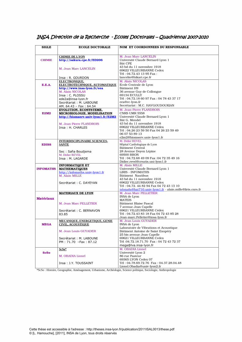
INSA Direction de la Recherche INSA Direction de la Recherche INSA Direction de la Recherche INSA Direction de la Recherche ---- Ecoles Doctorales Ecoles Doctorales Ecoles Doctorales Ecoles Doctorales –––– Quadriennal Quadriennal Quadriennal Quadriennal 2007200720072007----2010201020102010
SIGLE ECOLE DOCTORALE NOM ET COORDONNEES DU RESPONSABLE
CHIMIE
CHIMIE DE LYON http://sakura.cpe.fr/ED206
M. Jean Marc LANCELIN
Insa : R. GOURDON
M. Jean Marc LANCELIN Université Claude Bernard Lyon 1 Bât CPE 43 bd du 11 novembre 1918 69622 VILLEURBANNE Cedex Tél : 04.72.43 13 95 Fax : [email protected]
E.E.A.
ELECTRONIQUE, ELECTROTECHNIQUE, AUTOMATIQUE http://www.insa-lyon.fr/eea M. Alain NICOLAS
Insa : C. PLOSSU [email protected] Secrétariat : M. LABOUNE AM. 64.43 – Fax : 64.54
M. Alain NICOLAS Ecole Centrale de Lyon Bâtiment H9 36 avenue Guy de Collongue 69134 ECULLY Tél : 04.72.18 60 97 Fax : 04 78 43 37 17 [email protected] Secrétariat : M.C. HAVGOUDOUKIAN
E2M2
EVOLUTION, ECOSYSTEME, MICROBIOLOGIE, MODELISATION http://biomserv.univ-lyon1.fr/E2M2 M. Jean-Pierre FLANDROIS
Insa : H. CHARLES
M. Jean-Pierre FLANDROIS CNRS UMR 5558 Université Claude Bernard Lyon 1 Bât G. Mendel 43 bd du 11 novembre 1918 69622 VILLEURBANNE Cédex Tél : 04.26 23 59 50 Fax 04 26 23 59 49 06 07 53 89 13 [email protected]
EDISS
INTERDISCIPLINAIRE SCIENCES-SANTE Sec : Safia Boudjema M. Didier REVEL Insa : M. LAGARDE
M. Didier REVEL Hôpital Cardiologique de Lyon Bâtiment Central 28 Avenue Doyen Lépine 69500 BRON Tél : 04.72.68 49 09 Fax :04 72 35 49 16 [email protected]
INFOMATHS
INFORMATIQUE ET MATHEMATIQUES http://infomaths.univ-lyon1.fr M. Alain MILLE
Secrétariat : C. DAYEYAN
M. Alain MILLE Université Claude Bernard Lyon 1 LIRIS - INFOMATHS Bâtiment Nautibus 43 bd du 11 novembre 1918 69622 VILLEURBANNE Cedex Tél : 04.72. 44 82 94 Fax 04 72 43 13 10 [email protected] - [email protected]
Matériaux
MATERIAUX DE LYON M. Jean Marc PELLETIER
Secrétariat : C. BERNAVON 83.85
M. Jean Marc PELLETIER INSA de Lyon MATEIS Bâtiment Blaise Pascal 7 avenue Jean Capelle 69621 VILLEURBANNE Cédex Tél : 04.72.43 83 18 Fax 04 72 43 85 28 [email protected]
MEGA
MECANIQUE, ENERGETIQUE, GENIE CIVIL, ACOUSTIQUE M. Jean Louis GUYADER
Secrétariat : M. LABOUNE PM : 71.70 –Fax : 87.12
M. Jean Louis GUYADER INSA de Lyon Laboratoire de Vibrations et Acoustique Bâtiment Antoine de Saint Exupéry 25 bis avenue Jean Capelle 69621 VILLEURBANNE Cedex Tél :04.72.18.71.70 Fax : 04 72 43 72 37
ScSo
ScSo* M. OBADIA Lionel
Insa : J.Y. TOUSSAINT
M. OBADIA Lionel Université Lyon 2 86 rue Pasteur 69365 LYON Cedex 07 Tél : 04.78.69.72.76 Fax : 04.37.28.04.48 [email protected]
*ScSo : Histoire, Geographie, Aménagement, Urbanisme, Archéologie, Science politique, Sociologie, Anthropologie
Cette thèse est accessible à l'adresse : http://theses.insa-lyon.fr/publication/2011ISAL0013/these.pdf © [L. Hamouche], [2011], INSA de Lyon, tous droits réservés

ii
Cette thèse est accessible à l'adresse : http://theses.insa-lyon.fr/publication/2011ISAL0013/these.pdf © [L. Hamouche], [2011], INSA de Lyon, tous droits réservés
Author’s Publications and patents
� JOURNALS:
• Hamouche, Lahcen; Allard, Bruno; , "Low power options for 32nm always-on SRAM architecture", (Accepted for publication to) Solid-State ElectronicsJournal, 2011.
� INT. CONFERENCES:
• Hamouche, Lahcen; Allard, Bruno; , "PORTLESS low power mux architecturewith line hard duplication," International Memory Workshop (IMW), 2010 IEEEInternational , vol., no., pp.1-4, 16-19 May 2010 doi: 10.1109/IMW.2010.5488404
• Hamouche, Lahcen; Allard, Bruno; LAFONT Jean-christophe , "SRAM portlessbitcell and current-mode reading," Circuits and Systems (ISCAS), Proceedingsof 2010 IEEE International Symposium on , vol., no., pp.3865-3868, May 302010-June 2 2010 doi: 10.1109/ISCAS.2010.5537704
� Patents :
• Low power robust current mode sensing for 5T-portless SRAM, FR/ 28.07.09/FRA0955274
• Low power multiplexer architecture, FR/ 26.01.10/ FRA 1050487
� Rejected:
• Hamouche, Lahcen; Allard, Bruno; , "5T-Portless SRAM as a candidate for32nm always-on memory", Transactions on Very Large Scale Integration (TVLSI)journal.
Cette thèse est accessible à l'adresse : http://theses.insa-lyon.fr/publication/2011ISAL0013/these.pdf © [L. Hamouche], [2011], INSA de Lyon, tous droits réservés

Cette thèse est accessible à l'adresse : http://theses.insa-lyon.fr/publication/2011ISAL0013/these.pdf © [L. Hamouche], [2011], INSA de Lyon, tous droits réservés
Abstract
More and more specific applications are demanding large SRAM blocs in advancetechnologies. Particularly there is a need for always-on memories that consequentlymust be low energy consuming. For example mobile heterogeneous wireless networksare implementing multiple interfaces that are attached to concurrent networks at thesame time and therefore manage multiple IP addresses simultaneously. The largeamount of memory faces a serious problem of power consumption. The classical strat-egy of bloc extinction comes to a limit in effective energy saving and system dynamicperformances. There is then a need for true always-on but very low power SRAM. Be-sides the design of SRAM memories in advanced technology must take into accountthe problem of reliability in terms of Process-Voltage-Temperature (PVT) variabilities.
Manuscript reviews the technical and industrial challenges regarding embeddedSRAM, with a stress on power consumption. Always-on SRAMs offer a particularchallenging example. State of art compares SRAM architectures from various view-points:
• Performances versus PVT variability
• Robustness of migration in further technology nodes
• Tradeoffs between bit-cell and peripherals complexities
State of the art reviews the exploratory works on analytical modeling for vari-ability statistics
Chapter 3 wishes to discuss analytical modeling for variability statistic as a meanto simplify 32nm SRAM design. A proposal of modeling is presented to describethe statistical behavior of performance key parameters. Modeling is based on variousassumptions but enables to show clear limitations of several target design parameters.
Chapter 4 details a bit-cell alternative to a 6T, 7T, 8T. . . as a 5T bit-cell called5T-Portless SRAM. The performances and advantages of 5T-Portless rely on a currentmode operation that offers a large reduction in dynamic power consumption addition-ally to a low leakage bit-cell. Operation and performance parameters are discussedfrom simulation based on latest update 32nm Design-Kit (high-k metal gate).
Chapter 5 details the design of a memory cut with a special emphasis on linehardcopy, matrix options and required peripherals. Design yields the layout of a1024x64 (64kb) memory that is currently under fabrication. Results and characteri-zations will be included in this chapter and compared to simulation evaluations.
iv
Cette thèse est accessible à l'adresse : http://theses.insa-lyon.fr/publication/2011ISAL0013/these.pdf © [L. Hamouche], [2011], INSA de Lyon, tous droits réservés
Abstract
The conclusion chapter highlights the major contributions of the study and dis-cusses the various simplification assumptions to see possible limitations. It is con-cluded affirmatively about industrial interest of the 5T-Portless SRAM for always-onembedded applications. Perspectives concern the analytical modeling for statistical be-havior of SRAM as the Monte-Carlo approach is no more practicable. The migrationof the 5T-Portless SRAM may be already considered in advanced nodes.
PhD results have received the following attention:
• 2 patent claims with one international extension
• 2 communications in IEEE conferences ( ISCAS 2010, IMW 2010)
• 2 submitted articles to Journal of (Solid State Circuit and Microelectronic Jour-nal)
v
Cette thèse est accessible à l'adresse : http://theses.insa-lyon.fr/publication/2011ISAL0013/these.pdf © [L. Hamouche], [2011], INSA de Lyon, tous droits réservés
Résumé
De plus en plus d’applications spécifiques embarquées exigent de larges blocs de mé-moires statiques SRAM. En particulier il y a un besoin de mémoires incondition-nellement actives pour lesquelles la consommation d’énergie est un paramètre clé.Par exemple les réseaux sans fil hétérogènes sont caractérisés par plusieurs interfacestournées vers des réseaux différents, donc de multiples adresses IP simultanées. Unegrande quantité de mémoire est mobilisée et pose un sérieux problème de consom-mation d’énergie vis-à-vis de l’autonomie de système mobile. La stratégie classiqued’extinction des blocs mémoire momentanément non opérationnelle ne permet qu’uneréduction faible en consommation et limite les performances dynamiques du système.Il y a donc un réel besoin pour une mémoire toujours opérationnelle avec un très faiblebilan énergétique. Par ailleurs les technologies CMOS avancées posent le problème dela variabilité et la conception de mémoire SRAM doit aboutir à un niveau de fiabilitétrès grand.
Le manuscrit décrit les verrous techniques et industriels concernant la mémoireembarquée SRAM très faible consommation. Le cas de la mémoire toujours opéra-tionnelle représente un défi pertinent. Un état de l’art balaie les architectures SRAMavec plusieurs points de vue :
• Niveau des performances en fonction de la variabilité
• Capacité à la migration technologique
• Compromis entre les niveaux cellules et périphérie de la mémoire
L’état de l’art s’intéresse aux tentatives de modélisation statistique vis-à-vis dela variabilité.
Le chapitre 2 offre une discussion à propos de la modélisation analytique statis-tique comme moyen de simplification de la conception en 32nm. En introduisantquelques simplifications, des paramètres clé de la conception sont modélisés pour enobtenir des spécifications et en voir d’éventuelles limites.
Le chapitre 3 décrit une cellule alternative aux 6T , 7T et 8T, laquelle est ap-pelée 5T-Portless. Les avantages et les performances de cette cellule 5T-Portless re-pose sur son fonctionnement en mode courant à l’origine de la réduction significativede la consommation dynamique ajoutée à une cellule intrinsèquement peu fuiteuse.Le fonctionnement et l’analyse de performances sont basés sur des simulations et unDesign-Kit le plus à jour en 32nm.
vi
Cette thèse est accessible à l'adresse : http://theses.insa-lyon.fr/publication/2011ISAL0013/these.pdf © [L. Hamouche], [2011], INSA de Lyon, tous droits réservés
Résumé
Le chapitre 4 détaille la conception d’un bloc mémoire avec une attention par-ticulière pour la recopie analogique de ligne, les possibilités de mise en matrice etdifférents périphériques. Un démonstrateur de 64kb (1024x64b) a été dessiné enCMOS32nm. Les résultats expérimentaux viendront compléter le chapitre et serontcomparés à la simulation.
La conclusion générale reprend les résultats les plus significatifs et rediscute lesprincipales hypothèses. La conclusion est favorable quand à l’intérêt industriel de la5T-Portless comme mémoire embarquée toujours active. Les perspectives concernentla modélisation statistique sachant que l’approche Monte-Carlo n’est plus envisage-able, et la migration de la SRAM dans d’autres Design-Kits.
Les travaux ont donné lieu à :
• Deux dépôts de brevet francais repris en une extension internationale
• Deux articles de conférences IEEE ( ISCAS 2010, IMW 2010)
• Deux articles soumis à des journaux ( Solid State Circuit et MicroelectronicJournal)
vii
Cette thèse est accessible à l'adresse : http://theses.insa-lyon.fr/publication/2011ISAL0013/these.pdf © [L. Hamouche], [2011], INSA de Lyon, tous droits réservés
Contents
List of Figures x
List of Tables xiii
Abbreviations xiv
1 Introduction 1
2 State of art of eSRAM 52.1 6T SRAM . . . . . . . . . . . . . . . . . . . . . . . . . . . . . . . . 7
2.1.1 Read operation . . . . . . . . . . . . . . . . . . . . . . . . . 72.1.2 Write operation . . . . . . . . . . . . . . . . . . . . . . . . . 122.1.3 SRAM bit-cell sizing . . . . . . . . . . . . . . . . . . . . . . 132.1.4 Retention mode . . . . . . . . . . . . . . . . . . . . . . . . . 15
2.2 Power consumption and variability . . . . . . . . . . . . . . . . . . . 172.2.1 Variability and consumption of a SRAM bit-cell . . . . . . . 172.2.2 SRAM Periphery . . . . . . . . . . . . . . . . . . . . . . . . 262.2.3 Conclusion . . . . . . . . . . . . . . . . . . . . . . . . . . . 26
3 Modeling for variability 293.1 Yields and margins in SRAM . . . . . . . . . . . . . . . . . . . . . . 303.2 Discussion on modeling results . . . . . . . . . . . . . . . . . . . . . 38
4 PORTLESS BIT-CELL AND CURRENT MODE OPERATION 454.1 5T SRAM bit-cells . . . . . . . . . . . . . . . . . . . . . . . . . . . 454.2 5T-Portless bit-cell . . . . . . . . . . . . . . . . . . . . . . . . . . . 46
4.2.1 5T-Portless bit-cell parameters . . . . . . . . . . . . . . . . . 514.2.2 Wordline driver . . . . . . . . . . . . . . . . . . . . . . . . 51
4.3 Hard-line duplication technique . . . . . . . . . . . . . . . . . . . . 534.4 Portless Sense and Mux architecture . . . . . . . . . . . . . . . . . . 55
4.4.1 Current mode sensing and writing . . . . . . . . . . . . . . . 574.4.2 Low Power Mux structure . . . . . . . . . . . . . . . . . . . 58
viii
Cette thèse est accessible à l'adresse : http://theses.insa-lyon.fr/publication/2011ISAL0013/these.pdf © [L. Hamouche], [2011], INSA de Lyon, tous droits réservés
Contents
5 Test chip and simulation results 635.1 Test chip design . . . . . . . . . . . . . . . . . . . . . . . . . . . . . 65
5.1.1 Bit-cell to matrix array . . . . . . . . . . . . . . . . . . . . . 655.1.2 Control block . . . . . . . . . . . . . . . . . . . . . . . . . . 68
5.1.2.1 Pulse generator . . . . . . . . . . . . . . . . . . . 705.1.2.2 Signal Generator . . . . . . . . . . . . . . . . . . . 725.1.2.3 Word line driver: WLD . . . . . . . . . . . . . . . 73
5.1.3 Y decoder . . . . . . . . . . . . . . . . . . . . . . . . . . . . 745.1.4 Input/Output . . . . . . . . . . . . . . . . . . . . . . . . . . 77
5.2 Simulation results . . . . . . . . . . . . . . . . . . . . . . . . . . . . 795.2.1 Comparison with the 6T SRAM . . . . . . . . . . . . . . . . 87
5.3 Testchip Results . . . . . . . . . . . . . . . . . . . . . . . . . . . . . 895.3.1 Test Chip environnement . . . . . . . . . . . . . . . . . . . . 905.3.2 Portlesss Results . . . . . . . . . . . . . . . . . . . . . . . . 92
6 Conclusion 95
Bibliography 100
ix
Cette thèse est accessible à l'adresse : http://theses.insa-lyon.fr/publication/2011ISAL0013/these.pdf © [L. Hamouche], [2011], INSA de Lyon, tous droits réservés
List of Figures
2.1 6T SRAM bit-cell . . . . . . . . . . . . . . . . . . . . . . . . . . . . 82.2 6T Butterfly curve (32nm and typical condition simulation) . . . . . . 92.3 SNM evaluation by simulation . . . . . . . . . . . . . . . . . . . . . 92.4 Simulated SNM-curve for a CMOS 45nm SRAM under (a) process
variations, (b) power supply variations and (c) temperature variationsbetween -40◦C and +125◦C . . . . . . . . . . . . . . . . . . . . . . . 10
2.5 Butterfly curve for different sizes of 6T bit-cell in 32nm (simulationsby Mastar) . . . . . . . . . . . . . . . . . . . . . . . . . . . . . . . . 10
2.6 Tree of variation propagation from process to transistor and circuit . . 112.7 Transient simulation result of read and write operation : (a) simulation
without mismatch, (b) simulation with device mismatch . . . . . . . . 112.8 Write operation in 6T Bit-cell . . . . . . . . . . . . . . . . . . . . . . 122.9 Process corners according to the NMOS and PMOS Vth values . . . . 132.10 WM and SNM versus the ratio N=α/β . . . . . . . . . . . . . . . . 142.11 6T SRAM bit-cell lekage versus VDD in CMOS 32nm . . . . . . . . . 152.12 DVR, Leakage and dynamic power comparison . . . . . . . . . . . . 182.13 Most popular leakage reducing techniques . . . . . . . . . . . . . . . 192.14 simulation results of the reducing leakage techniques . . . . . . . . . 202.15 VDD scaling . . . . . . . . . . . . . . . . . . . . . . . . . . . . . . . 212.16 Negative bit-line . . . . . . . . . . . . . . . . . . . . . . . . . . . . 212.17 Word line boosting . . . . . . . . . . . . . . . . . . . . . . . . . . . 222.18 simulated 6T butterfly curve for VDD=1.2V and VDD=.8V . . . . . . 232.19 SNM simulation comparison for 32nm bit-cells . . . . . . . . . . . . 242.20 ∆VBL and VSAO distribution overlapping (Monte Carlo simulations) . 252.21 6T bit-cell Multiplexed structure . . . . . . . . . . . . . . . . . . . . 25
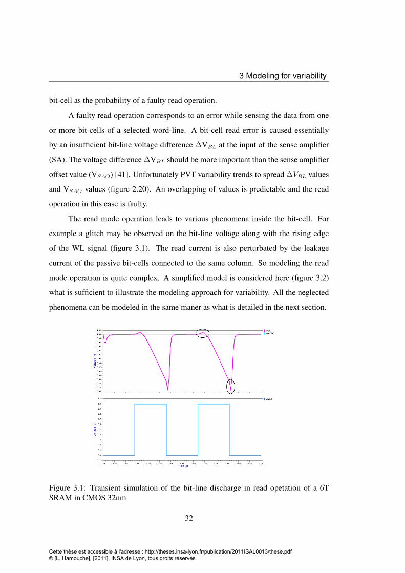
3.1 Transient simulation of the bit-line discharge in read opetation of a 6TSRAM in CMOS 32nm . . . . . . . . . . . . . . . . . . . . . . . . . 32
3.2 Bit-lines’ voltage difference during discharged time ta . . . . . . . . . 333.3 SRAM array with Y decoders and sense amplifier . . . . . . . . . . . 343.4 Distribution function of FZ(0) versus ta with CBL=200 fF . . . . . . . 373.5 VSAO and ∆VBL results of Monte Carlo simulation . . . . . . . . . . 393.6 Monte Carlo simulation results ∆VBL for different ta values . . . . . 413.7 µ∆VBL and σ∆VBL versus the discharge time ta . . . . . . . . . . . . . 41
x
Cette thèse est accessible à l'adresse : http://theses.insa-lyon.fr/publication/2011ISAL0013/these.pdf © [L. Hamouche], [2011], INSA de Lyon, tous droits réservés
List of Figures
3.8 ta margin variation with a 10% σ increasing . . . . . . . . . . . . . . 42
4.1 Schematic and simulated SNM of 45nm 5T asymmetric SRAM (a,c)and 5T Portless SRAM (b,d) . . . . . . . . . . . . . . . . . . . . . . 46
4.2 Portless bit-cell: (a) schematic, (b) layout . . . . . . . . . . . . . . . 474.3 Portless current in read operation . . . . . . . . . . . . . . . . . . . . 474.4 BFC comparison of Monte Carlo simulation with N=104 iteration be-
tween 6T (a) and Portless (b) and gaussian distribution fit (c) . . . . . 484.5 leakage comparison between 6T and Portless bit-cells . . . . . . . . 494.6 Monte Carlo simulation results of Iread for a typical PVT corner in
CMOS 32nm . . . . . . . . . . . . . . . . . . . . . . . . . . . . . . 504.7 Portless bit-cell parameters . . . . . . . . . . . . . . . . . . . . . . . 524.8 ∆VR and Iread Versus VAXS . . . . . . . . . . . . . . . . . . . . . . 524.9 PMOS, NMOS Voltage divider . . . . . . . . . . . . . . . . . . . . 534.10 simulation results of WLD in different PVT corners . . . . . . . . . 544.11 Charge pump circuit and the Word-Lline Driver with RP and WP signal
sets . . . . . . . . . . . . . . . . . . . . . . . . . . . . . . . . . . . 544.12 Proposal of Portless bit-cell arrangement . . . . . . . . . . . . . . . . 564.13 Bit-line and internal nodes voltage in read and write operation . . . . 574.14 Porrtless bit-cell column with IOcell . . . . . . . . . . . . . . . . . . 594.15 Mux bit-cells and Sense . . . . . . . . . . . . . . . . . . . . . . . . 604.16 Vaxs and cells’ internal node voltages during a write operation in a
CMOS32nm Portless arrangement . . . . . . . . . . . . . . . . . . . 614.17 Portless multiplexer architecture . . . . . . . . . . . . . . . . . . . . 62
5.1 Schematic of the 5T-Portless memory cut . . . . . . . . . . . . . . . 645.2 5T-Portless bit-cell, schematic (a), layout (b) . . . . . . . . . . . . . 665.3 Mux cell layout (a) and schematic (b) . . . . . . . . . . . . . . . . . 675.4 precharge circuit (a) layout (b) schematic . . . . . . . . . . . . . . . 685.5 The Sub-matrix column arragement . . . . . . . . . . . . . . . . . . 695.6 Sub-matrix array of 32×64, Mux cell, dummy line and precharge circuit 695.7 Pulse diagram generation according to write or read operations . . . . 705.8 Control blocks with different input output signals . . . . . . . . . . . 715.9 VAXS and OAXS in both write and read operation generated by WP
and WP . . . . . . . . . . . . . . . . . . . . . . . . . . . . . . . . . 725.10 WLD block with different input and output signals . . . . . . . . . . 745.11 Cell’s internal nodes voltages and AXS signals in both write and read
operations . . . . . . . . . . . . . . . . . . . . . . . . . . . . . . . . 755.12 Ydecoder for both sub-matrix word line selection and sub-matrix se-
lection . . . . . . . . . . . . . . . . . . . . . . . . . . . . . . . . . . 765.13 Local decoder and predecoder layout . . . . . . . . . . . . . . . . . . 76
xi
Cette thèse est accessible à l'adresse : http://theses.insa-lyon.fr/publication/2011ISAL0013/these.pdf © [L. Hamouche], [2011], INSA de Lyon, tous droits réservés
List of Figures
5.14 Layout of the sub-matrix including Matrix array, Control block, Mux,and Ydecoder . . . . . . . . . . . . . . . . . . . . . . . . . . . . . . 77
5.15 Schematic and layout of IOcell with Q and Q output data and D andD input data . . . . . . . . . . . . . . . . . . . . . . . . . . . . . . 78
5.16 Cut layout with the 32 sub-matrices and Inpu/Output interfaces . . . . 785.17 Bit effective area . . . . . . . . . . . . . . . . . . . . . . . . . . . . 795.18 A critical path in the matrix array with the critical bit-cells to be simulated 805.19 Simulation of read and write operations for the full memory cut using
the xasimulator . . . . . . . . . . . . . . . . . . . . . . . . . . . . . 825.20 Simulation results for the read delay (Critical Path simulation with Eldo 825.21 Bit-cell read current for different PVT corners . . . . . . . . . . . . . 835.22 Leakage current difference induced by a bit-cell in the retention mode
and the total bit-cell leakage in both FS and SF corners . . . . . . . . 845.23 Bit-cell leakage in different PVT corners, simulated by Eldo in CMOS
32nm . . . . . . . . . . . . . . . . . . . . . . . . . . . . . . . . . . 855.24 Dynamic power consumption during a read operation in different PVT
corners . . . . . . . . . . . . . . . . . . . . . . . . . . . . . . . . . . 865.25 Comparison of 6T SRAM column and Portless column . . . . . . . . 875.26 Current waveforms during read and write operations in both 6T and
Portless SRAM . . . . . . . . . . . . . . . . . . . . . . . . . . . . . 885.27 Portless CUT with other memories and logical IPs . . . . . . . . . . . 905.28 Values of ION of NMOS and PMOS given by the CAD and test chip
measurements . . . . . . . . . . . . . . . . . . . . . . . . . . . . . . 915.29 Test chip results for the full cut leakage current . . . . . . . . . . . . 935.30 Test chip dynamic current measurements and CAD values for the full
memory cut. . . . . . . . . . . . . . . . . . . . . . . . . . . . . . . . 93
xii
Cette thèse est accessible à l'adresse : http://theses.insa-lyon.fr/publication/2011ISAL0013/these.pdf © [L. Hamouche], [2011], INSA de Lyon, tous droits réservés

Cette thèse est accessible à l'adresse : http://theses.insa-lyon.fr/publication/2011ISAL0013/these.pdf © [L. Hamouche], [2011], INSA de Lyon, tous droits réservés
List of Tables
3.1 some values of Y LN
versus ta . . . . . . . . . . . . . . . . . . . . . . 373.2 transistor threshold voltage Vth value and standard deviation across
different technology nodes . . . . . . . . . . . . . . . . . . . . . . . 40
5.1 Testchip PVT Specification . . . . . . . . . . . . . . . . . . . . . . 655.2 Simplified logical equations for AXS, LAXS, GAXS, OAXS signals 735.3 Extracted parameters from the critical path simulation . . . . . . . . . 815.4 Hard line duplication delay in different PVT corners . . . . . . . . . . 835.5 Bit-cell leakage values for different process corners in case of (VDD=1V,
Temp=25◦C ) . . . . . . . . . . . . . . . . . . . . . . . . . . . . . . 845.6 Bit-cell leakage values for different process corners in case of (VDD=1.1V,
Temp= 125◦C) . . . . . . . . . . . . . . . . . . . . . . . . . . . . . 855.7 Bit-cell leakage values for different process corners in case of (VDD=0.9V,
Temp= -40◦C) . . . . . . . . . . . . . . . . . . . . . . . . . . . . . 855.8 Bit-cell leakage values in typical, fastest and slowest corners . . . . . 855.9 Dynamic power consumption of the full cut in typical and worst case
corners . . . . . . . . . . . . . . . . . . . . . . . . . . . . . . . . . . 865.10 Leakage current values comparison between Portless and 6T SRAM
bit-cells . . . . . . . . . . . . . . . . . . . . . . . . . . . . . . . . . 895.11 Leakage current values comparison between Portless and 6T SRAM
bit-cells . . . . . . . . . . . . . . . . . . . . . . . . . . . . . . . . . 89
xiii
Cette thèse est accessible à l'adresse : http://theses.insa-lyon.fr/publication/2011ISAL0013/these.pdf © [L. Hamouche], [2011], INSA de Lyon, tous droits réservés

Cette thèse est accessible à l'adresse : http://theses.insa-lyon.fr/publication/2011ISAL0013/these.pdf © [L. Hamouche], [2011], INSA de Lyon, tous droits réservés

Abbreviations
SRAM Static Random Access MemoryCMOS Complementary metal oxide semi-conductorPU Pull UpPD Pull DownPG Pass GateBLT Bit-Line TrueBLF Bit-Line FalseLBL Local Bit-linesGBL Global Bit-linesSA Sense AmplifierSNM Static Noise MarginWM Write MarginIread Bit-Cell read CurrentPVT Process Voltage TemperatureMC Monte CarloVth threshold VoltageDRV Data Retention VoltageRBB Reverse Body BiasFBB Forward Body Bias∆VBL Bit-Line Voltage differenceVSAO Sense Amplifier Offsetσ Standard deviationµ Average ValueRYL Read Operation YieldAQL Acceptable Quality Levelta Bit-Line discharge delayWLD Word Line DriverGcell Global Mux-cell bit-cellLcell Local Mux-cell bit-cellIOcell Input Output CellVAXSread VAXS voltage for the read operation
xiv
Cette thèse est accessible à l'adresse : http://theses.insa-lyon.fr/publication/2011ISAL0013/these.pdf © [L. Hamouche], [2011], INSA de Lyon, tous droits réservés
List of Tables
VAXSwrite VAXS voltage for the write operationMSB Most Significant BitLSB Least Significant BitRO Ring oscillatorsDRC Design Rule CheckLVS Layout Versus Schematic
xv
Cette thèse est accessible à l'adresse : http://theses.insa-lyon.fr/publication/2011ISAL0013/these.pdf © [L. Hamouche], [2011], INSA de Lyon, tous droits réservés
1
Introduction
Today, systems on Chip are always a fast growing market. They embedded more and
more complex functions that require an increasing memory capacity. The Static Ran-
dom Access Memory SRAM is the mostly used solution where either bandwidth or
low power, or both are principal considerations. SRAM is a type of semiconductor
memory where the word static indicates that, unlike dynamic RAM (DRAM) [1], it
does not need to be periodically refreshed, as SRAM uses bistable latching circuitry to
store each bit. SRAM exhibits data remanence, but is still volatile in the conventional
sense that data is eventually lost when the memory is not powered. SRAM is also eas-
ier to control (interface to) and generally more truly random access than modern types
of DRAM.
An SRAM cell has three different states it can be in: standby when the circuit
is idle, reading when the data has been requested and writing when updating the con-
tents. The SRAM to operate in read mode and write mode should have read- stability
and write-ability respectively. Both conditions become difficult to satisfy in advanced
technologies because of the high degree of variability in thin CMOS transistor param-
eter, essentially technologies beyond 45nm. Increasing the memory size makes the
required degree of reliability hard to please. This makes the first challenge for the
SRAMs in advanced technology nodes.
The power consumption increases with the advanced CMOS technologies. CMOS
scaling requires not only very low threshold voltages to retain the device switching
speeds, but also ultra-thin gate oxides to maintain the current drive and keep thresh-
old voltage variations under control when dealing with short-channel effects. Low
1
Cette thèse est accessible à l'adresse : http://theses.insa-lyon.fr/publication/2011ISAL0013/these.pdf © [L. Hamouche], [2011], INSA de Lyon, tous droits réservés
1 Introduction
threshold voltage results in an exponential increase in the sub-threshold leakage cur-
rent which contributes to the static power consumption. Charging/discharging large
bit-lines’ capacitance represents a large portion of power consumption during a write
or read operations, which represents the dynamic power. Static and Dynamic power
consumption increases with the advanced CMOS technology nodes. This make the
second challenge for the SRAMs in advanced technology nodes.
On-chip cache memory consumes a large percentage of the whole chip area and
power consumption and expectes to increase in advanced technologies [2]. The power
consumption of SRAM varies widely depending on how frequently it is accessed; it
can be as power-hungry as dynamic RAM, when used at high frequencies, and some
ICs can consume many watts at full bandwidth. On the other hand, static RAM used
at a somewhat slower pace, such as in applications with moderately clocked micropro-
cessors, draw very little power and can have a nearly negligible power consumption
when sitting idle, in the region of a few micro-watts.
Static RAM exists primarily as general purpose products with asynchronous in-
terface, such as the 28 pin 32Kx8 chips (usually named XXC256), and similar products
up to 16 Mbit per chip. With synchronous interface, usually used for caches and other
applications requiring burst transfers, up to 18 Mbit (256Kx72) per chip. Secondary as
integrated on chip as RAM or cache memory in micro-controllers (usually from around
32 bytes up to 128 kilobytes). Finally as the primary caches in powerful microproces-
sors, such as the x86 family, and many others (from 8 kB, up to several megabytes).
To store the registers and parts of the state-machines used in some microprocessors or
in application specific ICs, or ASICs (usually in the order of kilobytes) SRAM is used
also in FPGAs and CPLDs (usually in the order of a few kilobytes or less).
Besides many applications require always-on memories and the power consump-
tion issue can be dramatic. When the amount of memory became large, no particular
technique is required providing that the power consumption is small compared to the
2
Cette thèse est accessible à l'adresse : http://theses.insa-lyon.fr/publication/2011ISAL0013/these.pdf © [L. Hamouche], [2011], INSA de Lyon, tous droits réservés
system global power. Besides power consumption in memories brings in the front pos-
sible thermal problems like Negative Biasing Thermal Instability (NBTI). When the
amount of memory becomes large there are two basic approaches to limit the power
consumption. If possible any unused memory is set into a deep sleep mode.
In a heterogeneous overlay wireless network, a mobile node (MN) with multiple
wireless interfaces can attach to various networks and obtains multiple IP addresses
simultaneously. To allow correspondent nodes to connect to a mobile node at anytime
through any mobile nodes’ IP address, an mobile node must keep its interfaces awake
to receive incoming packets. Unfortunately, studies indicate that power consumption
of a mobile node with multiple interfaces poses a serious problem [3], even when
interfaces are idle. The energy-conserving always-on schemes for a mobile node with
multiple interfaces is to only maintain one awake interface and turn off completely
other interfaces to minimize its power consumption [4]. The main limitation is the
necessity of a robust restoring scheme to avoid packet losses. The same complex
approach has been applied to cache memories [5] where turn-off is not practicable
and only a fraction of excessive power consumption is saved. The same global issue is
true for real-time embedded systems [6]: the usage of SDRAM memory for working
context storage enables a power consumption saving with a sufficiently fast wake-up,
but memory content is preserved with self-refresh mechanism. Turning-off unused
amount of memory shows limitations; a trade-off between power saving and content
preservation or wake-up speed must be set. Whatever there are systems where the
latter approach is event not applicable. There is then a need for true always-on but
very low-power SRAM.
A practical technique to limit power consumption in embedded applications is to
turn-off unuseful blocks. There is then a trade-off between the wake-up requirements,
the possible reduction in consumption and the complexity of the power management
controller. Wireless applications suffer now from the lack of effectiveness of the latter
3
Cette thèse est accessible à l'adresse : http://theses.insa-lyon.fr/publication/2011ISAL0013/these.pdf © [L. Hamouche], [2011], INSA de Lyon, tous droits réservés
1 Introduction
technique, i.e. a robust restoring scheme to avoid packet losses. The same complex
approach has been applied to cache memories where turn-off is not practicable and
only a small fraction of excessive power consumption is saved. Power reduction is
unfortunately essential in embedding systems so the need for true always-on but very
low-power SRAM is emerging.
The PhD thesis focuses On the Always-on low power SRAM memories (essen-
tially low dynamic power) in thin CMOS technology node CMOS 32nm and beyond.
chapter 2 reviews the state of the art of the eSRAM and describes different techniques
to reduce the static and dynamic power consumption with respect the variability issue.
Main techniques of power reduction are reviewed with their contributions and their
limitations. Chapter 3 presents a discussion about a statistical variability modeling and
the variability effects on the yield. In Chapter 4 an original low power architecture
based on 5T-Portless bit-cell is presented, with current mode read/write operations, as
an ideal candidate for the always-on SRAM memories. A test chip implementation in
CMOS 32nm of the 5T-Porless is detailed in Chapter 5 and a comparison with an exist-
ing 6T SRAM memory is presented based on simulation. Chapter 5 presents some test
chip functionality results and power consumption. Finally the conclusion in Chapter 6
highlights the major contributions of the study and discusses the various simplification
assumptions to see possible limitations. It is concluded affirmatively about industrial
interest of the 5T-Portless SRAM for always-on embedded applications. Perspectives
concern the analytical modeling for statistical behavior of SRAM as the Monte-Carlo
approach is no more practicable. The migration of the 5T-Portless SRAM may be
already considered in advanced nodes
4
Cette thèse est accessible à l'adresse : http://theses.insa-lyon.fr/publication/2011ISAL0013/these.pdf © [L. Hamouche], [2011], INSA de Lyon, tous droits réservés
2
State of art of eSRAM
Moore’s law, which could be interpreted as a cost reduction law, has been followed
successfully for more than thirty years. It is the reduction in the size of elementary
transistor (area is divided by half each 18 months) that has allowed this [7]. Never-
theless, it is now very difficult to maintain the same pace due to physical limitations
related to size reduction.
The level of accuracy necessary to fabricate a circuit is necessary higher with
successive technology nodes, and it is becoming critical. Small variations affect each
step in the manufacturing process and these variations are gaining importance in terms
of parasitic effects. When a circuit is fabricated, several characteristics are monitored
in order to follow the variations of the process: a lot-to-lot variation is measured and a
wafer-to-wafer variation. Only global variations are thus monitored while variations at
transistor levels are local. Both global and local variations influence the circuit perfor-
mances, hence the manufacturing yield [8]. The semiconductor industry can no longer
count on the reduction of the transistors’ size from generation to generation, there-
fore it requires to find new paradigms to continue the scale reduction. At each new
technological node, some of the initially insignificant physical limitations become im-
portant: the dispersion of performances is now the main difficulty in designing SRAM
circuits. Even if the industry manages to fabricate chips with over one billion of the
smallest transistors and increasing number of inputs-outputs, pertinent applications are
5
Cette thèse est accessible à l'adresse : http://theses.insa-lyon.fr/publication/2011ISAL0013/these.pdf © [L. Hamouche], [2011], INSA de Lyon, tous droits réservés
2 State of art of eSRAM
paradoxally seldom found that require such an amount of these tiny devices. The de-
velopment cost for each new technology node grows exponentially at each step and
a pause in Moore’s law seems to be inevitable [9]. At 32nm, pad rings of one thou-
sand I/Os will be common and the circuit size (amount of transistors) necessary to fill
these I/O rings will be enormous and will pose several problems such as manufacturing
yield limitations, thermal issues, etc. To improve manufacturing yield, it is necessary
to envision the effects of all random variations, i.e. to quantify the variability of vari-
ous phenomena, and then to implement solutions to limit the effect of this variability,
either at technology or design levels.
The huge systems to be invented are predicted to embed a large amount of mem-
ories. Among all types of memory, the embedded Static Random Access Memory (eS-
RAM) is a key product. Numerous SRAM bit-cells exist that are suitable for specific
applications. The topic of the thesis focuses always-on and possibly low frequency op-
eration eSRAMs. Whatever the variability issues remain the limiting factor that push
to invent new architectures of bit-cells and memory peripherals to enable satisfying
manufacturing yield in 32nm CMOS and beyond.
The state of art of eSRAM is discussed from various points of view to enlighten
the hard trade-offs between the layout of the bit-cell, its operations and the additional
circuits to assist the operations, the density, the power consumption and finally the
success to reject the effects of variability. The discussion begins with the six-transistor
SRAM (6T SRAM) as a reference bit-cell and the published techniques to limit the
effect of variability. The power consumption of the SRAMs is discussed but unfor-
tunately the variability limits the efficiency of the industrial techniques to limit the
power consumption. Finally the five-transistor bit-cell is proposed as an interesting
alternative but in a configuration called 5T-Portless.
6
Cette thèse est accessible à l'adresse : http://theses.insa-lyon.fr/publication/2011ISAL0013/these.pdf © [L. Hamouche], [2011], INSA de Lyon, tous droits réservés
2.1 6T SRAM
2.1 6T SRAM
The static random-access memories (SRAM) are most widely used, due to their high
performance: microprocessors may contain up to 70% of SRAMs in transistor count
or area. The trend in the semiconductor market is to push for more integration and
more size reduction: the development and optimization of a technological node is
more and more difficult and expensive. The reduction in size of a SRAM circuit in
coming nodes is nonetheless complex and it faces several limitations. The reliability
of the SRAM bit-cell is degraded with ever smaller technologies and the device func-
tionality is endangered. Designing SRAM circuits in CMOS 32nm requires technical
and technological solutions to overcome the size reduction limitations, while insuring
satisfactory functionality, with a guaranteed reliability so that it can be economically
fabricated.
The manufacturing of a standard SRAM is fully compatible with CMOS core
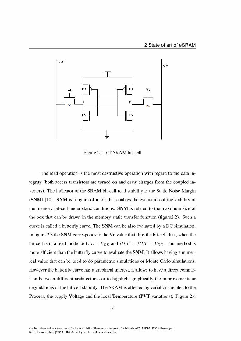
processes. The standard SRAM bit-cell is based on a 6-transistor arrangement: it
is called a 6T-SRAM. Two CMOS inverters, formed by PU and PD transistors, are
connected, one opposite to the other, and two access transistors, PG transistors, are
added (figure 2.1). Three possible operations are: writing a bit data, retaining the bit
data and reading the bit data. The operation is controlled through the word-lines that
activate or block the access transistors PG, so that there is, or not, a connection to the
bit-lines BLT and BLF that propagate the bit value from or to the bit-cell.
2.1.1 Read operation
During a read operation, the bit-lines are floating and converges to the potential dictated
by the bit-cell when the word-line is properly activated: one bit-line is discharged to
ensure the high speed and low power read operation. The voltage between bit-lines’
potentials is sensed by a voltage sense amplifier SA.
7
Cette thèse est accessible à l'adresse : http://theses.insa-lyon.fr/publication/2011ISAL0013/these.pdf © [L. Hamouche], [2011], INSA de Lyon, tous droits réservés
2 State of art of eSRAM
Figure 2.1: 6T SRAM bit-cell
The read operation is the most destructive operation with regard to the data in-
tegrity (both access transistors are turned on and draw charges from the coupled in-
verters). The indicator of the SRAM bit-cell read stability is the Static Noise Margin
(SNM) [10]. SNM is a figure of merit that enables the evaluation of the stability of
the memory bit-cell under static conditions. SNM is related to the maximum size of
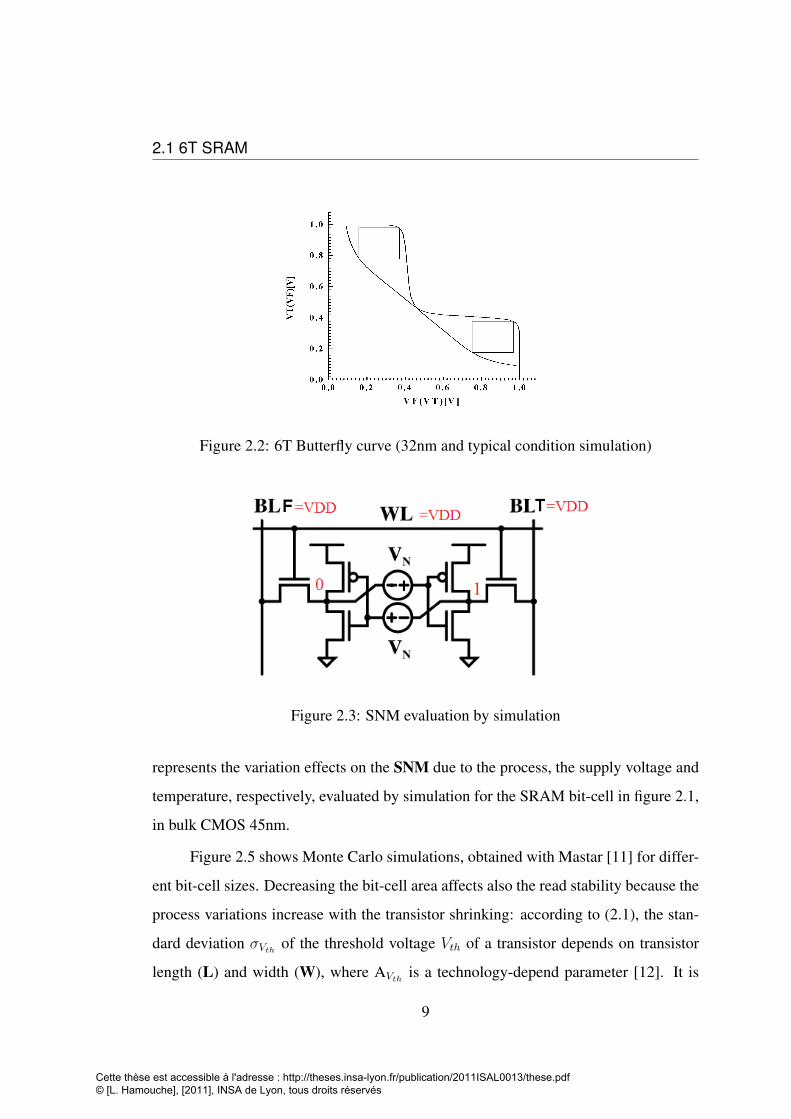
the box that can be drawn in the memory static transfer function (figure2.2). Such a
curve is called a butterfly curve. The SNM can be also evaluated by a DC simulation.
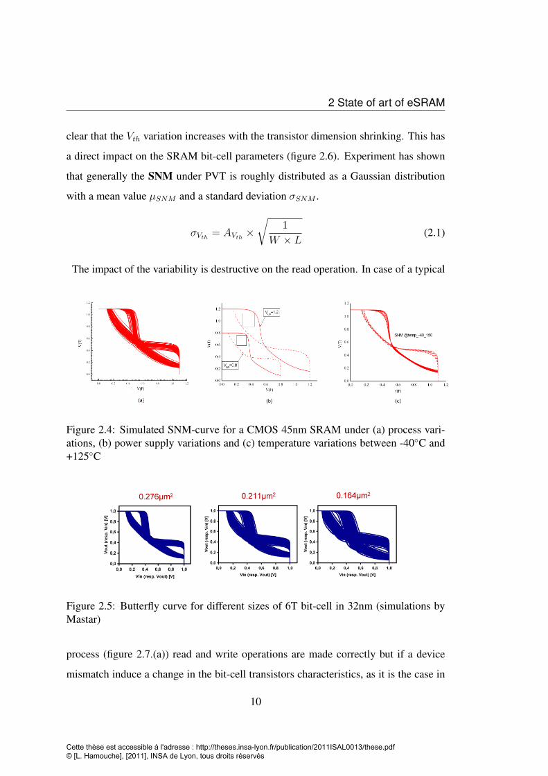
In figure 2.3 the SNM corresponds to the Vn value that flips the bit-cell data, when the
bit-cell is in a read mode i.e WL = VDD and BLF = BLT = VDD. This method is
more efficient than the butterfly curve to evaluate the SNM. It allows having a numer-
ical value that can be used to do parametric simulations or Monte Carlo simulations.
However the butterfly curve has a graphical interest, it allows to have a direct compar-
ison between different architectures or to highlight graphically the improvements or
degradations of the bit-cell stability. The SRAM is affected by variations related to the
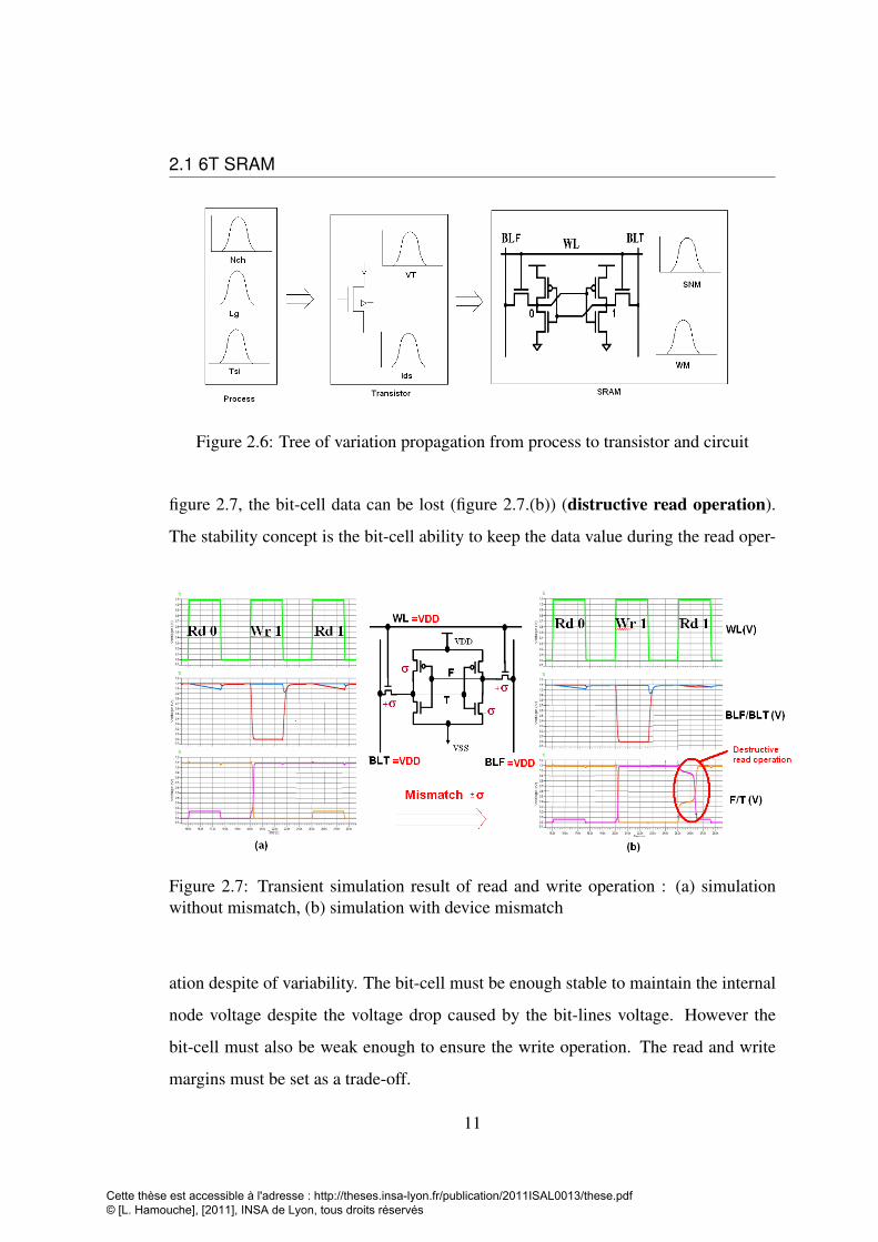
Process, the supply Voltage and the local Temperature (PVT variations). Figure 2.4
8
Cette thèse est accessible à l'adresse : http://theses.insa-lyon.fr/publication/2011ISAL0013/these.pdf © [L. Hamouche], [2011], INSA de Lyon, tous droits réservés
2.1 6T SRAM
Figure 2.2: 6T Butterfly curve (32nm and typical condition simulation)
Figure 2.3: SNM evaluation by simulation
represents the variation effects on the SNM due to the process, the supply voltage and
temperature, respectively, evaluated by simulation for the SRAM bit-cell in figure 2.1,
in bulk CMOS 45nm.
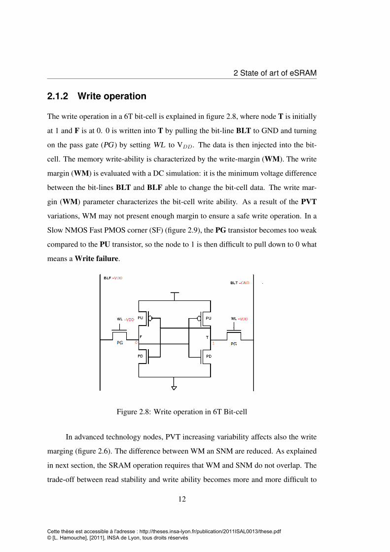
Figure 2.5 shows Monte Carlo simulations, obtained with Mastar [11] for differ-
ent bit-cell sizes. Decreasing the bit-cell area affects also the read stability because the
process variations increase with the transistor shrinking: according to (2.1), the stan-
dard deviation σVth of the threshold voltage Vth of a transistor depends on transistor
length (L) and width (W), where AVth is a technology-depend parameter [12]. It is
9
Cette thèse est accessible à l'adresse : http://theses.insa-lyon.fr/publication/2011ISAL0013/these.pdf © [L. Hamouche], [2011], INSA de Lyon, tous droits réservés
2 State of art of eSRAM
clear that the Vth variation increases with the transistor dimension shrinking. This has
a direct impact on the SRAM bit-cell parameters (figure 2.6). Experiment has shown
that generally the SNM under PVT is roughly distributed as a Gaussian distribution
with a mean value µSNM and a standard deviation σSNM .
σVth = AVth ×√
1
W × L(2.1)
The impact of the variability is destructive on the read operation. In case of a typical
Figure 2.4: Simulated SNM-curve for a CMOS 45nm SRAM under (a) process vari-ations, (b) power supply variations and (c) temperature variations between -40◦C and+125◦C
Figure 2.5: Butterfly curve for different sizes of 6T bit-cell in 32nm (simulations byMastar)
process (figure 2.7.(a)) read and write operations are made correctly but if a device
mismatch induce a change in the bit-cell transistors characteristics, as it is the case in
10
Cette thèse est accessible à l'adresse : http://theses.insa-lyon.fr/publication/2011ISAL0013/these.pdf © [L. Hamouche], [2011], INSA de Lyon, tous droits réservés
2.1 6T SRAM
Figure 2.6: Tree of variation propagation from process to transistor and circuit
figure 2.7, the bit-cell data can be lost (figure 2.7.(b)) (distructive read operation).
The stability concept is the bit-cell ability to keep the data value during the read oper-
Figure 2.7: Transient simulation result of read and write operation : (a) simulationwithout mismatch, (b) simulation with device mismatch
ation despite of variability. The bit-cell must be enough stable to maintain the internal
node voltage despite the voltage drop caused by the bit-lines voltage. However the
bit-cell must also be weak enough to ensure the write operation. The read and write
margins must be set as a trade-off.
11
Cette thèse est accessible à l'adresse : http://theses.insa-lyon.fr/publication/2011ISAL0013/these.pdf © [L. Hamouche], [2011], INSA de Lyon, tous droits réservés
2 State of art of eSRAM
2.1.2 Write operation
The write operation in a 6T bit-cell is explained in figure 2.8, where node T is initially
at 1 and F is at 0. 0 is written into T by pulling the bit-line BLT to GND and turning
on the pass gate (PG ) by setting WL to VDD. The data is then injected into the bit-
cell. The memory write-ability is characterized by the write-margin (WM). The write
margin (WM) is evaluated with a DC simulation: it is the minimum voltage difference
between the bit-lines BLT and BLF able to change the bit-cell data. The write mar-
gin (WM) parameter characterizes the bit-cell write ability. As a result of the PVT
variations, WM may not present enough margin to ensure a safe write operation. In a
Slow NMOS Fast PMOS corner (SF) (figure 2.9), the PG transistor becomes too weak
compared to the PU transistor, so the node to 1 is then difficult to pull down to 0 what
means a Write failure.
Figure 2.8: Write operation in 6T Bit-cell
In advanced technology nodes, PVT increasing variability affects also the write
marging (figure 2.6). The difference between WM an SNM are reduced. As explained
in next section, the SRAM operation requires that WM and SNM do not overlap. The
trade-off between read stability and write ability becomes more and more difficult to
12
Cette thèse est accessible à l'adresse : http://theses.insa-lyon.fr/publication/2011ISAL0013/these.pdf © [L. Hamouche], [2011], INSA de Lyon, tous droits réservés
2.1 6T SRAM
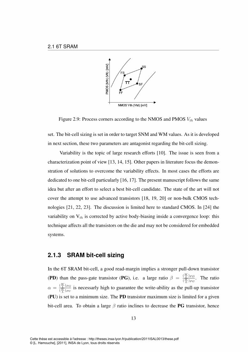
Figure 2.9: Process corners according to the NMOS and PMOS Vth values
set. The bit-cell sizing is set in order to target SNM and WM values. As it is developed
in next section, these two parameters are antagonist regarding the bit-cell sizing.
Variability is the topic of large research efforts [10]. The issue is seen from a
characterization point of view [13, 14, 15]. Other papers in literature focus the demon-
stration of solutions to overcome the variability effects. In most cases the efforts are
dedicated to one bit-cell particularly [16, 17]. The present manuscript follows the same
idea but after an effort to select a best bit-cell candidate. The state of the art will not
cover the attempt to use advanced transistors [18, 19, 20] or non-bulk CMOS tech-
nologies [21, 22, 23]. The discussion is limited here to standard CMOS. In [24] the
variability on Vth is corrected by active body-biasing inside a convergence loop: this
technique affects all the transistors on the die and may not be considered for embedded
systems.
2.1.3 SRAM bit-cell sizing
In the 6T SRAM bit-cell, a good read-margin implies a stronger pull-down transistor
(PD) than the pass-gate transistor (PG), i.e. a large ratio β =(WL
)PD
(WL
)PG. The ratio
α =(WL
)PG
(WL
)PUis necessarly high to guarantee the write-ability as the pull-up transistor
(PU) is set to a minimum size. The PD transistor maximum size is limited for a given
bit-cell area. To obtain a large β ratio inclines to decrease the PG transistor, hence
13
Cette thèse est accessible à l'adresse : http://theses.insa-lyon.fr/publication/2011ISAL0013/these.pdf © [L. Hamouche], [2011], INSA de Lyon, tous droits réservés
2 State of art of eSRAM
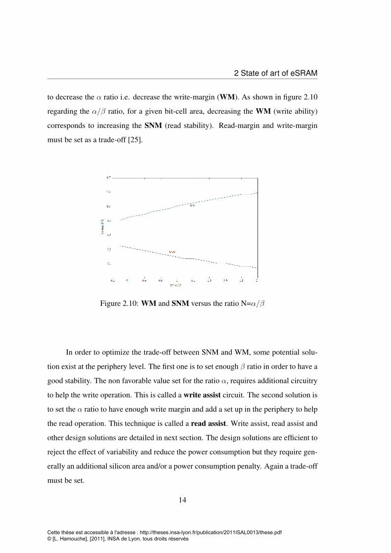
to decrease the α ratio i.e. decrease the write-margin (WM). As shown in figure 2.10
regarding the α/β ratio, for a given bit-cell area, decreasing the WM (write ability)
corresponds to increasing the SNM (read stability). Read-margin and write-margin
must be set as a trade-off [25].
Figure 2.10: WM and SNM versus the ratio N=α/β
In order to optimize the trade-off between SNM and WM, some potential solu-
tion exist at the periphery level. The first one is to set enough β ratio in order to have a
good stability. The non favorable value set for the ratio α, requires additional circuitry
to help the write operation. This is called a write assist circuit. The second solution is
to set the α ratio to have enough write margin and add a set up in the periphery to help
the read operation. This technique is called a read assist. Write assist, read assist and
other design solutions are detailed in next section. The design solutions are efficient to
reject the effect of variability and reduce the power consumption but they require gen-
erally an additional silicon area and/or a power consumption penalty. Again a trade-off
must be set.
14
Cette thèse est accessible à l'adresse : http://theses.insa-lyon.fr/publication/2011ISAL0013/these.pdf © [L. Hamouche], [2011], INSA de Lyon, tous droits réservés
2.1 6T SRAM
2.1.4 Retention mode
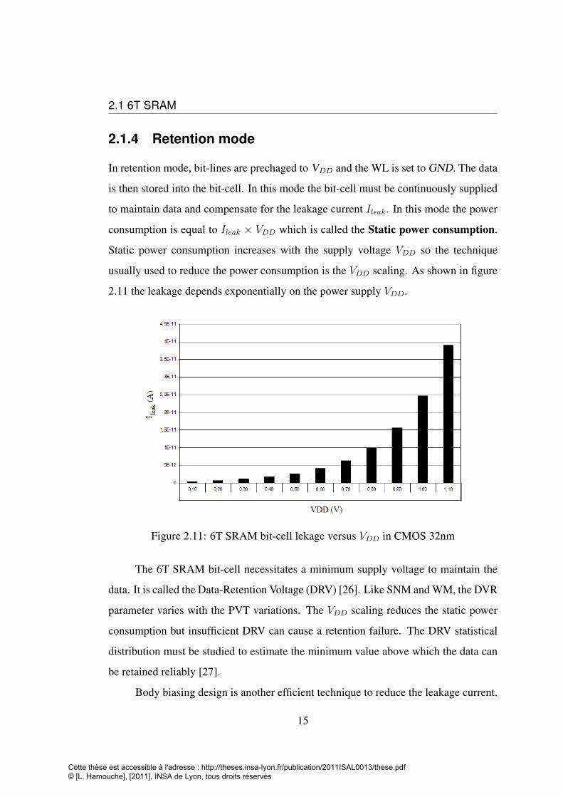
In retention mode, bit-lines are prechaged to VDD and the WL is set to GND. The data
is then stored into the bit-cell. In this mode the bit-cell must be continuously supplied
to maintain data and compensate for the leakage current Ileak. In this mode the power
consumption is equal to Ileak × VDD which is called the Static power consumption.
Static power consumption increases with the supply voltage VDD so the technique
usually used to reduce the power consumption is the VDD scaling. As shown in figure
2.11 the leakage depends exponentially on the power supply VDD.
Figure 2.11: 6T SRAM bit-cell lekage versus VDD in CMOS 32nm
The 6T SRAM bit-cell necessitates a minimum supply voltage to maintain the
data. It is called the Data-Retention Voltage (DRV) [26]. Like SNM and WM, the DVR
parameter varies with the PVT variations. The VDD scaling reduces the static power
consumption but insufficient DRV can cause a retention failure. The DRV statistical
distribution must be studied to estimate the minimum value above which the data can
be retained reliably [27].
Body biasing design is another efficient technique to reduce the leakage current.
15
Cette thèse est accessible à l'adresse : http://theses.insa-lyon.fr/publication/2011ISAL0013/these.pdf © [L. Hamouche], [2011], INSA de Lyon, tous droits réservés
2 State of art of eSRAM
The leakage depends to the value of the threshold voltage Vth of a transistor. According
to (2.2) [28], the threshold voltage can be increased by changing the voltage value of
the transistor’s body. That technique is called the body biasing.
Vth = VFB + (Φs0 −∆Φs) + γ√φs0 − VBS
(1− λXd
L
)(2.2)
In next section VDD scaling and body biasing techniques are compared. This tech-
nique requires generation of different supply voltage levels. Additional circuitry area
is needed and additional power consumption is engendered. The interest of these tech-
niques depends potentially on the dedicated memory application.
Variations of gate length (L), gate width (W), gate oxide thickness (Tox), and
the channel dopant concentration (Na) increase with the technology scaling, thus the
random variation of the MOSFET threshold voltage increases while its value dimin-
ishes to retain the device switching speed with the technology scaling. Variability on
Vth has been demonstrated to vary more rapidly since CMOS 90nm [29]. The SRAM
functionality margin is negatively affected [30, 31]. The transistor leakage current in-
creases with technology scaling and its values can affect the SRAM data in retention
mode. This is an additional but indirect limitation [32] that sets the minimal value of
power supply in retention mode (DVR).
It appears that there are 3 ways to lessen the fluctuations: namely reducing the
technology-dependent parameters, increasing the transistor geometrical factor or intro-
ducing design-level improvements. The latter is related to design options. The former
is related to technology process. The geometrical factor is incompatible with Moore’s
law and ITRS roadmap. The only scalable solutions, apart from an improved technol-
ogy (which will come in time), are based on design improvements.
Next section reviews the existing design techniques to reduce the power con-
16
Cette thèse est accessible à l'adresse : http://theses.insa-lyon.fr/publication/2011ISAL0013/these.pdf © [L. Hamouche], [2011], INSA de Lyon, tous droits réservés
2.2 Power consumption and variability
sumption and reject the effects of variability. It details different solutions that can be
applied at bit-cell, bit-cell array and at periphery level respectively.
2.2 Power consumption and variability
Power consumption in memories is the sum of dynamic and static power. Dynamic
power is the power needed to ensure different operations (read, write, decoding. . . ). It
depends on the number of operations made in a working time. The static power, which
is the power due mainly to the transistors’ leakage, is always present as long as the
memory is biased. The power consumption of a chip can be modeled by (2.3) where
C is the bit-lines and parasitic effective capacitances, VDD is the supply voltage, Ileak
the full chip leakage current and f the operating frequency of the circuit.
P = C × V 2DD × f + Ileak × VDD (2.3)
As discussed previously, the total power is a function of VDD. The mostly used
technique to reduce the power consumption is VDD scaling. In advanced CMOS tech-
nology nodes, transistor’s leakage increases exponentially due to the rapid scaling of
transistor channel and length for each successive technology [32]. Additionally the size
of the memories continues to increase, thus the static and dynamic power consumption
of the memory becomes more and more important.
2.2.1 Variability and consumption of a SRAM bit-cell
In retention mode, leakage is the main power consumption. The memory sleep mode
consists in decreasing the matrix voltage (bit-cells’ supply voltage) and/or switch-off
the periphery supply voltage. The major contribution to leakage is the bit-cell array.
The leakage depends on the bit-cell architecture. In [33] a comparison between 6T, 8T
17
Cette thèse est accessible à l'adresse : http://theses.insa-lyon.fr/publication/2011ISAL0013/these.pdf © [L. Hamouche], [2011], INSA de Lyon, tous droits réservés
2 State of art of eSRAM
and 9T bit-cells in terms of Static Noise Margin SNM, Write Margin WM, DRV and
leakage is presented. Figure 2.12 shows a comparison of static and dynamic power for
6T, 8T and 9T structures respectively, obtained by simulation. Each bit-cell has been
layouted with minimal area in 32nm standard CMOS.
Figure 2.12: DVR, Leakage and dynamic power comparison
Since 9T is more stable than 8T and 8T is more stable than 6T, DRV of 9T is
the lowest and thus offers less leakage than the other bit-cells. However 9T has more
parasitic capacitances so its dynamic power is larger. The memory global consumption
depends on the type of dedicated application. If the memory is frequently operating
and has short retention time, dynamic power is the major contributor to the memory
global consumption and 6T SRAM bit-cell is then favorable. If the memory is not
frequently operating and period of retention is the major state in the memory working
time, then leakage is the major contributor of the full chip power consumption. In this
case bit-cells like 9T or 8T are the best candidate.
Leakage, as discussed previously, can be scaled according to VDD or acting on
the transistor’s body voltage. Three techniques exist to reduce the leakage (figure 2.13)
18
Cette thèse est accessible à l'adresse : http://theses.insa-lyon.fr/publication/2011ISAL0013/these.pdf © [L. Hamouche], [2011], INSA de Lyon, tous droits réservés
2.2 Power consumption and variability
• Reverse Body Bias (RBB): the PMOS transistors’ body (VDDs) initially con-
nected to VDD is supplied with higher voltage and NMOS transistors’ body
(GNDs) initially connected to GND is supplied with a lower voltage. The initial
power voltage (VDD and GND) are kept unchanged.
• Source Body Bias: the body power supplies (VDDs and GNDs) are kept un-
changed but VDD is decreased and GND is increased.
• VDD scaling (VS): both power supply (VDD) and body power supplies (VDDs)
are reduced.
Figure 2.13: Most popular leakage reducing techniques
The most efficient technique to reduce the leakage is the source body bias (SBB)
as shown in figure 2.14, but this technique reduce considerably the bit-cell power sup-
ply and the retention capability. The most stable solution regarding the data retention
is the reverse body bias (RBB). It offers a reduction in power supply without scaling
the bit-cell voltage supply.
19
Cette thèse est accessible à l'adresse : http://theses.insa-lyon.fr/publication/2011ISAL0013/these.pdf © [L. Hamouche], [2011], INSA de Lyon, tous droits réservés
2 State of art of eSRAM
Figure 2.14: simulation results of the reducing leakage techniques
Dynamic power can be reduced also by decreasing VDD but this can arises prob-
lems in the read stability by reduction of the Static Noise Margin (SNM ). Write ability
can also be damaged by reduction of the Write Margin (WM ) [34]. Read assist and
write assist can help to ensure safe write or read operations at low VDD respectively.
There are 3 main write assist techniques:
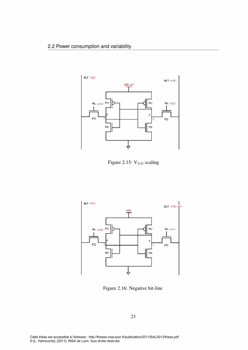
• Supply down scaling (Figure 2.15): it consists in reducing the bit-cell supply to
VDD- ∆V to obtain a less stable bit-cell. PU transistor is weakened versus PG,
so the write ability is improved.
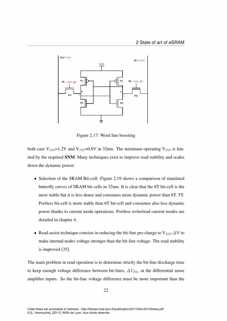
• Negative bit-line (Figure 2.16): the bit-line BL is set to GND- ∆V to create a
stronger PG transistor and enable to flip the bit-cell easily.
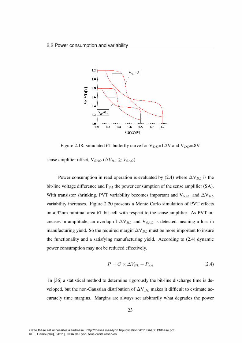
• World line boosting (Figure 2.17): PG can be stronger by increasing WL volt-
age, the current sinking is more important and the write operation is made rapidly.
These techniques allow to perform write functionality at low VDD supply so the dy-
namic power is reduced. Reducing VDD affects also the read stability. SNM decreases
as far as VDD declines. Figure 2.18 shows the simulated 6T bit-cell butterfly curve for
20
Cette thèse est accessible à l'adresse : http://theses.insa-lyon.fr/publication/2011ISAL0013/these.pdf © [L. Hamouche], [2011], INSA de Lyon, tous droits réservés
2.2 Power consumption and variability
Figure 2.15: VDD scaling
Figure 2.16: Negative bit-line
21
Cette thèse est accessible à l'adresse : http://theses.insa-lyon.fr/publication/2011ISAL0013/these.pdf © [L. Hamouche], [2011], INSA de Lyon, tous droits réservés
2 State of art of eSRAM
Figure 2.17: Word line boosting
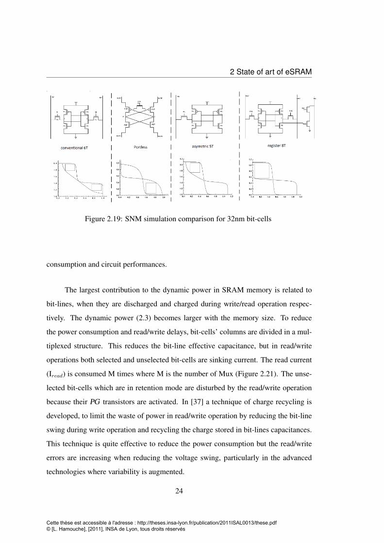
both case VDD=1.2V and VDD=0.8V in 32nm. The minimum operating VDD is lim-
ited by the required SNM. Many techniques exist to improve read stability and scales
down the dynamic power:
• Selection of the SRAM Bit-cell: Figure 2.19 shows a comparison of simulated
butterfly curves of SRAM bit-cells in 32nm. It is clear that the 8T bit-cell is the
most stable but it is less dense and consumes more dynamic power than 6T. 5T-
Portless bit-cell is more stable than 6T bit-cell and consumes also less dynamic
power thanks to current mode operations. Portless write/read current modes are
detailed in chapter 4.
• Read-assist technique consists in reducing the bit-line pre-charge to VDD-∆V to
make internal nodes voltage stronger than the bit-line voltage. The read stability
is improved [35].
The main problem in read operation is to determine strictly the bit-line discharge time
to keep enough voltage difference between bit-lines, ∆VBL, at the differential sense
amplifier inputs. So the bit-line voltage difference must be more important than the
22
Cette thèse est accessible à l'adresse : http://theses.insa-lyon.fr/publication/2011ISAL0013/these.pdf © [L. Hamouche], [2011], INSA de Lyon, tous droits réservés
2.2 Power consumption and variability
Figure 2.18: simulated 6T butterfly curve for VDD=1.2V and VDD=.8V
sense amplifier offset, VSAO (∆VBL ≥ VSAO).
Power consumption in read operation is evaluated by (2.4) where ∆VBL is the
bit-line voltage difference and PSA the power consumption of the sense amplifier (SA).
With transistor shrinking, PVT variability becomes important and VSAO and ∆VBL
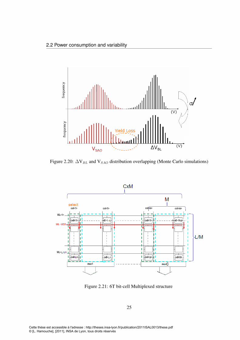
variability increases. Figure 2.20 presents a Monte Carlo simulation of PVT effects
on a 32nm minimal area 6T bit-cell with respect to the sense amplifier. As PVT in-
creases in amplitude, an overlap of ∆VBL and VSAO is detected meaning a loss in
manufacturing yield. So the required margin ∆VBL must be more important to insure
the functionality and a satisfying manufacturing yield. According to (2.4) dynamic
power consumption may not be reduced effectively.
P = C ×∆VBL + PSA (2.4)
In [36] a statistical method to determine rigorously the bit-line discharge time is de-
veloped, but the non-Gaussian distribution of ∆VBL makes it difficult to estimate ac-
curately time margins. Margins are always set arbitrarily what degrades the power
23
Cette thèse est accessible à l'adresse : http://theses.insa-lyon.fr/publication/2011ISAL0013/these.pdf © [L. Hamouche], [2011], INSA de Lyon, tous droits réservés
2 State of art of eSRAM
Figure 2.19: SNM simulation comparison for 32nm bit-cells
consumption and circuit performances.
The largest contribution to the dynamic power in SRAM memory is related to
bit-lines, when they are discharged and charged during write/read operation respec-
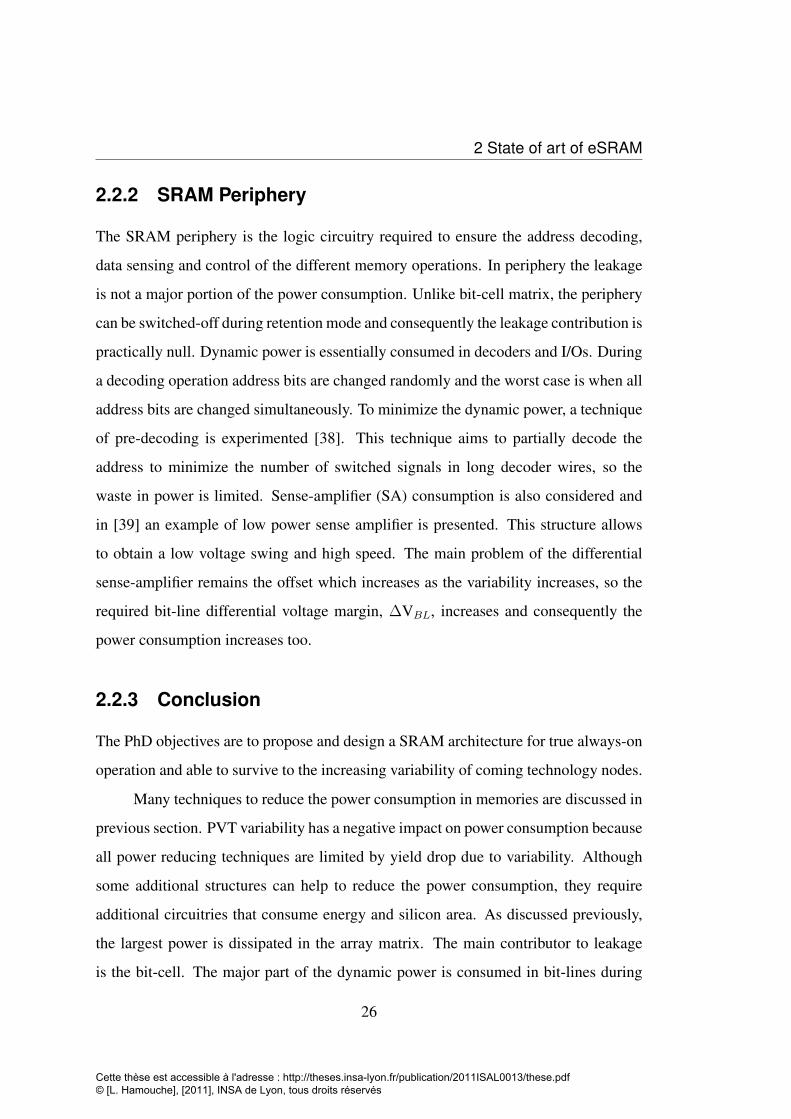
tively. The dynamic power (2.3) becomes larger with the memory size. To reduce
the power consumption and read/write delays, bit-cells’ columns are divided in a mul-
tiplexed structure. This reduces the bit-line effective capacitance, but in read/write
operations both selected and unselected bit-cells are sinking current. The read current
(Iread) is consumed M times where M is the number of Mux (Figure 2.21). The unse-
lected bit-cells which are in retention mode are disturbed by the read/write operation
because their PG transistors are activated. In [37] a technique of charge recycling is
developed, to limit the waste of power in read/write operation by reducing the bit-line
swing during write operation and recycling the charge stored in bit-lines capacitances.
This technique is quite effective to reduce the power consumption but the read/write
errors are increasing when reducing the voltage swing, particularly in the advanced
technologies where variability is augmented.
24
Cette thèse est accessible à l'adresse : http://theses.insa-lyon.fr/publication/2011ISAL0013/these.pdf © [L. Hamouche], [2011], INSA de Lyon, tous droits réservés
2.2 Power consumption and variability
Figure 2.20: ∆VBL and VSAO distribution overlapping (Monte Carlo simulations)
Figure 2.21: 6T bit-cell Multiplexed structure
25
Cette thèse est accessible à l'adresse : http://theses.insa-lyon.fr/publication/2011ISAL0013/these.pdf © [L. Hamouche], [2011], INSA de Lyon, tous droits réservés
2 State of art of eSRAM
2.2.2 SRAM Periphery
The SRAM periphery is the logic circuitry required to ensure the address decoding,
data sensing and control of the different memory operations. In periphery the leakage
is not a major portion of the power consumption. Unlike bit-cell matrix, the periphery
can be switched-off during retention mode and consequently the leakage contribution is
practically null. Dynamic power is essentially consumed in decoders and I/Os. During
a decoding operation address bits are changed randomly and the worst case is when all
address bits are changed simultaneously. To minimize the dynamic power, a technique
of pre-decoding is experimented [38]. This technique aims to partially decode the
address to minimize the number of switched signals in long decoder wires, so the
waste in power is limited. Sense-amplifier (SA) consumption is also considered and
in [39] an example of low power sense amplifier is presented. This structure allows
to obtain a low voltage swing and high speed. The main problem of the differential
sense-amplifier remains the offset which increases as the variability increases, so the
required bit-line differential voltage margin, ∆VBL, increases and consequently the
power consumption increases too.
2.2.3 Conclusion
The PhD objectives are to propose and design a SRAM architecture for true always-on
operation and able to survive to the increasing variability of coming technology nodes.
Many techniques to reduce the power consumption in memories are discussed in
previous section. PVT variability has a negative impact on power consumption because
all power reducing techniques are limited by yield drop due to variability. Although
some additional structures can help to reduce the power consumption, they require
additional circuitries that consume energy and silicon area. As discussed previously,
the largest power is dissipated in the array matrix. The main contributor to leakage
is the bit-cell. The major part of the dynamic power is consumed in bit-lines during
26
Cette thèse est accessible à l'adresse : http://theses.insa-lyon.fr/publication/2011ISAL0013/these.pdf © [L. Hamouche], [2011], INSA de Lyon, tous droits réservés
2.2 Power consumption and variability
read/write operation.
• There is a need for a low leakage bit-cell which allows low dynamic power,
without degrading stability. It is essential for the PhD objectives.
• Moreover the voltage sense operation is limited by constraints on the voltage
sense amplifier offset (VSAO). The bit-lines capacitance charge and discharge are
associated to power consumption difficult to decrease. An alternative technique
must be considered.
• The usefulness of assist circuit is based on the possibility to tune the power sup-
ply without impact on the bit-cell operations. The many trade-off in the design
are even more complex to define. A safe approach is to be demonstrated.
We come to the conclusion that a current mode operation is a candidate to solve most
of the pervious limitations. The 5T-Portless bit-cell has already been presented for this
major improvement. Unfortunately literature indicates that the Portless is not industri-
ally interesting beyond 45nm.
Chapter 4 details a new 5T-Portless SRAM structure where the technology
limitations has been overcome thanks to a new set of operating points. The bit-cell
is less leaky than the 6T SRAM and permits to have a read/write operation based on
original current mode operations called the hard-line copy.
The design of the 5T-Portless bit-cell faces the same ever limitations with respect
to variability. The work presented in chapter 4 has led to a reflexion about an alternative
method to Monte-Carlo simulation. In chapter 3 is presented a tentative modeling
approach to take variability into account prior to design effort. This chapter is isolated
from the Portless issues and details a study of variability modeling developed for the 6T
SRAM margins. the relations between margins and yield is discussed with a projection
in advanced technology nodes.
27
Cette thèse est accessible à l'adresse : http://theses.insa-lyon.fr/publication/2011ISAL0013/these.pdf © [L. Hamouche], [2011], INSA de Lyon, tous droits réservés
2 State of art of eSRAM
Chapter 5 details a test chip design and presents a comparative simulation results
with 6T-SRAM in standard 32nm CMOS. Few experimental results are detailed in
Chapter 5.
28
Cette thèse est accessible à l'adresse : http://theses.insa-lyon.fr/publication/2011ISAL0013/these.pdf © [L. Hamouche], [2011], INSA de Lyon, tous droits réservés
3
Modeling for variability
In a CMOS technology node, process variations are quantified as a mean value and a
standard deviation of a given transistor physical parameter (transistor geometry L and
W , Na dopant chanel concentration, gate oxide thickness Tox . . . ). Indeed variations
at circuit level are not estimated using a direct or explicit method, i.e. functions like
P = f(L,W,Na, Tox...), where P is a given functional parameter, like the SNM for
the SRAM bit-cell for example. Such functions are difficult to determine but they
would ease the design of circuits with an implicit consideration of variability effects.
The design of any sub-block of a large circuit is more efficient when it is based on solid
specification values. In the case of SRAM, the specifications are for example SNM,
WM . . ., i.e. circuits parameters as opposed to transistor parameters and technology
parameters.
In fact a designer develops solutions based on experiment in a trial-correction
manner. The effects of variability are evaluated throughout expensive Monte Carlo
simulations. A Monte Carlo simulation is a set of a predefined simulation scheme
where the physical parameters of the transistor models are tuned randomly. The circuit
parameters values change over the simulation iterations. The distribution of a given
parameter P values is approximated generally as a Gaussian shape of mean value µP
and standard deviation σP . These representations of the cell parameters are used by
the designer to set margins to satisfy a manufacturing yield target. The design exercise
29
Cette thèse est accessible à l'adresse : http://theses.insa-lyon.fr/publication/2011ISAL0013/these.pdf © [L. Hamouche], [2011], INSA de Lyon, tous droits réservés
3 Modeling for variability
may be time consuming in the case of intricate trade-offs between the various margins.
The designer has no way to prove that a trade-off is optimal. Moreover the parameter
distributions are not necessarily Gaussian. This introduces inaccuracies and a satisfy-
ing trade-off for a designer may reveal actually a failure with respect to manufacturing
yield.
In advanced CMOS technology nodes, larger margins in SRAM bit-cell are re-
quired to face variability increases. There is a penalty in bit-cell performances and
density. In [40] authors are engaged to increase the SRAM bit-cell supply voltage to
limit the sensitivity of the bit-cell to variability. There is a direct penalty on power con-
sumption on one hand, and there is a severe limitation to this method with advanced
technology nodes on the other hand. There is a need for an alternative design paradigm
and the parameter functions P as proposed here-above seem to be a first step. It is now
proposed a tentative method to explicit such parameter functions P and yield pertinent
values for the SRAM margins prior to the design effort.
3.1 Yields and margins in SRAM
Usually SRAM margin prediction is difficult to perform. It is a trade-off between
performances and reliability and manufacturing yield. A design performance is the
measurement of the guarantee of a targeted yield. It means to achieve enough SRAM
margins, no more no less. The manufacturing yield concept may be defined in relation
to the probability to have a wrong operation (read, write or retention) in a SRAM cir-
cuit. It is considered globally at a system level. Unfortunately margins are set at the
bit-cell design level. The main problematic in the circuit design is the ability to quan-
tify margins at the cell design level that are required for a given chip manufacturing
yield while featuring maximal performances, i.e. to make the ideal optimization.
A SRAM manufacturing yield may be quantitatively appreciated with an explicit
value, namely the Acceptable Quality Level (AQL), or implicitly in terms of Gaussian
30
Cette thèse est accessible à l'adresse : http://theses.insa-lyon.fr/publication/2011ISAL0013/these.pdf © [L. Hamouche], [2011], INSA de Lyon, tous droits réservés
3.1 Yields and margins in SRAM
distribution. AQL means a maximum number of defective bit-cells per billion of fab-
ricated bit-cells. An issue is to translate this maximum number of defective bit-cells
into quantitative values for acceptable fluctuations, and to work out solutions to meet
the manufacturing yield constraint. For example a typical AQL value for 10 Megabit
of SRAM bit-cells could be 100 ppm. If one million of circuits of 10Mb bit-cells is
considered, it is not allowed more than 100 defective bit-cells globally thus the AQL
evaluation in (3.1).
100 defective bit-cells106 circuits× 10.106 bits
= 10−11 (3.1)
The manufacturing yield may also be expressed as the necessary distribution of
good circuits. The previous AQL value of 10−11 is translated into a requirement for
functional circuits up to 7σ from the nominal process values. Improvements in SRAM
design are sometimes presented in term of gain in sigmas. In literature it means that
the proposed improvement enables to save initially bad circuits up to a certain number
of sigma from the nominal process values.
In this chapter the example of the SRAM read operation is detailed and the re-
lationship between the delay margin and the reading yield is explicated. The reading
yield (RYL) is the probability to have a read success in a memory of N=n×m bits (fig-
ure 3.3) with a given delay margin needful for bit-lines discharging. The delay must
be long enough to ensure a targeted yield but it must be as short as possible to ensure
maximal performances: reducing power consumption and guarantee a good operation
speed.
By an abuse of language, the read or write yield refer to the probability of a fault
instead of the probability of success. Of course one quantity translates easily into the
other. From now on, it is detailed an explicit expression of the read yield in a SRAM
31
Cette thèse est accessible à l'adresse : http://theses.insa-lyon.fr/publication/2011ISAL0013/these.pdf © [L. Hamouche], [2011], INSA de Lyon, tous droits réservés
3 Modeling for variability
bit-cell as the probability of a faulty read operation.
A faulty read operation corresponds to an error while sensing the data from one
or more bit-cells of a selected word-line. A bit-cell read error is caused essentially
by an insufficient bit-line voltage difference ∆VBL at the input of the sense amplifier
(SA). The voltage difference ∆VBL should be more important than the sense amplifier
offset value (VSAO) [41]. Unfortunately PVT variability trends to spread ∆VBL values
and VSAO values (figure 2.20). An overlapping of values is predictable and the read
operation in this case is faulty.
The read mode operation leads to various phenomena inside the bit-cell. For
example a glitch may be observed on the bit-line voltage along with the rising edge
of the WL signal (figure 3.1). The read current is also perturbated by the leakage
current of the passive bit-cells connected to the same column. So modeling the read
mode operation is quite complex. A simplified model is considered here (figure 3.2)
what is sufficient to illustrate the modeling approach for variability. All the neglected
phenomena can be modeled in the same maner as what is detailed in the next section.
Figure 3.1: Transient simulation of the bit-line discharge in read opetation of a 6TSRAM in CMOS 32nm
32
Cette thèse est accessible à l'adresse : http://theses.insa-lyon.fr/publication/2011ISAL0013/these.pdf © [L. Hamouche], [2011], INSA de Lyon, tous droits réservés
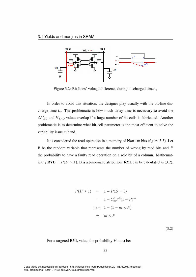
3.1 Yields and margins in SRAM
Figure 3.2: Bit-lines’ voltage difference during discharged time ta
In order to avoid this situation, the designer play usually with the bit-line dis-
charge time ta. The problematic is how much delay time is necessary to avoid the
∆VBL and VSAO values overlap if a huge number of bit-cells is fabricated. Another
problematic is to determine what bit-cell parameter is the most efficient to solve the
variability issue at hand.
It is considered the read operation in a memory of N=n×m bits (figure 3.3). Let
B be the random variable that represents the number of wrong by read bits and P
the probability to have a faulty read operation on a sole bit of a column. Mathemat-
ically RYL = P (B ≥ 1). B is a binomial distribution. RYL can be calculated as (3.2).
P (B ≥ 1) = 1− P (B = 0)
= 1− C0mP
0(1− P )m
≈= 1− (1−m× P )
= m× P
(3.2)
For a targeted RYL value, the probability P must be:
33
Cette thèse est accessible à l'adresse : http://theses.insa-lyon.fr/publication/2011ISAL0013/these.pdf © [L. Hamouche], [2011], INSA de Lyon, tous droits réservés
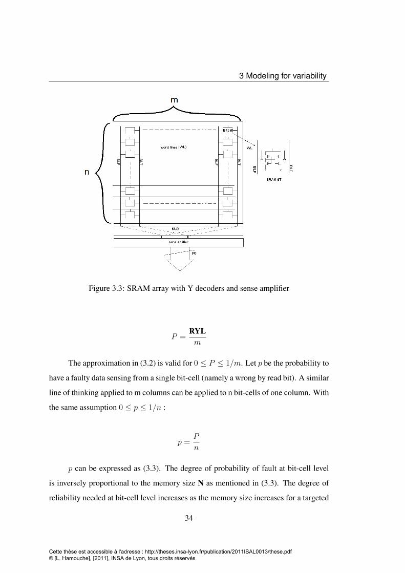
3 Modeling for variability
Figure 3.3: SRAM array with Y decoders and sense amplifier
P =RYLm
The approximation in (3.2) is valid for 0 ≤ P ≤ 1/m. Let p be the probability to
have a faulty data sensing from a single bit-cell (namely a wrong by read bit). A similar
line of thinking applied to m columns can be applied to n bit-cells of one column. With
the same assumption 0 ≤ p ≤ 1/n :
p =P
n
p can be expressed as (3.3). The degree of probability of fault at bit-cell level
is inversely proportional to the memory size N as mentioned in (3.3). The degree of
reliability needed at bit-cell level increases as the memory size increases for a targeted
34
Cette thèse est accessible à l'adresse : http://theses.insa-lyon.fr/publication/2011ISAL0013/these.pdf © [L. Hamouche], [2011], INSA de Lyon, tous droits réservés
3.1 Yields and margins in SRAM
yield RYL.
p =RYLn×m
=RYL
N(3.3)
With the PVT variation, bit-line voltage difference ∆VBL and the sense amplifier
offset VSAO vary correspondingly. Both parameters can be considered as continuous
random variables. The probability p can be expressed as explained in (3.4):
p = P (∆VBL ≤ VSAO)
=
∫ +∞
−∞fSAO(ν)F∆VBL(ν)dν
(3.4)
Where fSAO is the probability density function of VSAO and F∆VBL is the distribution
function of the bit-line voltage difference ∆VBL.
The voltage difference ∆VBL is obtained when the bit-line capacitances are discharged
by the bit-cell’s pull-down transistor PD through the pass-gate transistor PG during a
time-period ta, called discharged time (figure.3.2). Relationship between ∆VBL and ta
is given in (3.5) where Iread is the bit-cell read current and CBL is the bit-line effective
capacitance. Considering Iread constant, ∆VBL can be considered as a linear function
of the discharge time ta.
∆VBL =Iread · taCBL
(3.5)
The probability p expressed in (3.4 ) is then :
p = P
(Iread · taCBL
≤ VSAO
)(3.6)
The parameter RYLN can be identified as the AQL discussed previously with respect to
read operation. AQL can be expressed as (3.7):
AQL =RYL
N= P
(Iread · taCBL
≤ VSAO
)(3.7)
35
Cette thèse est accessible à l'adresse : http://theses.insa-lyon.fr/publication/2011ISAL0013/these.pdf © [L. Hamouche], [2011], INSA de Lyon, tous droits réservés
3 Modeling for variability
The main target in expressing a matrix read yield in function of cell parameters is first
to estimate the required reliability at the cell level to accomplish an acceptable global
read operation yield. Second to have the degree of sensitivity of the read yield versus
the discharge time ta, which is a parameter set by the designer. In next paragraph
the global read yield is expressed as a function of the discharge time ta with several
assumptions.
Let Z be a random variable defined as:
Z =Iread · taCBL
− VSAO
RYL can be expressed as (3.8):
RYLN
= P
(Iread · taCBL
≤ VSAO
)= P (Z ≤ 0) (3.8)
Considering Iread and VSAO as Gaussian variables, Z is also a Gaussian variable with
mean value µZ and the standard variation σZ as:
µZ =µIread × ta
CBL− µSAO
and
σZ =
√(σIread × ta
CBL
)2
+ σ2SAO
Equation 3.8 becames:RYL
N= P (Z ≤ 0) = FZ(0) (3.9)
where FZ is the distribution function of the Z variable. Z depends on the bit-lines’
discharge time ta, so determining the delay margin time, revert to solve equation (3.10)
36
Cette thèse est accessible à l'adresse : http://theses.insa-lyon.fr/publication/2011ISAL0013/these.pdf © [L. Hamouche], [2011], INSA de Lyon, tous droits réservés
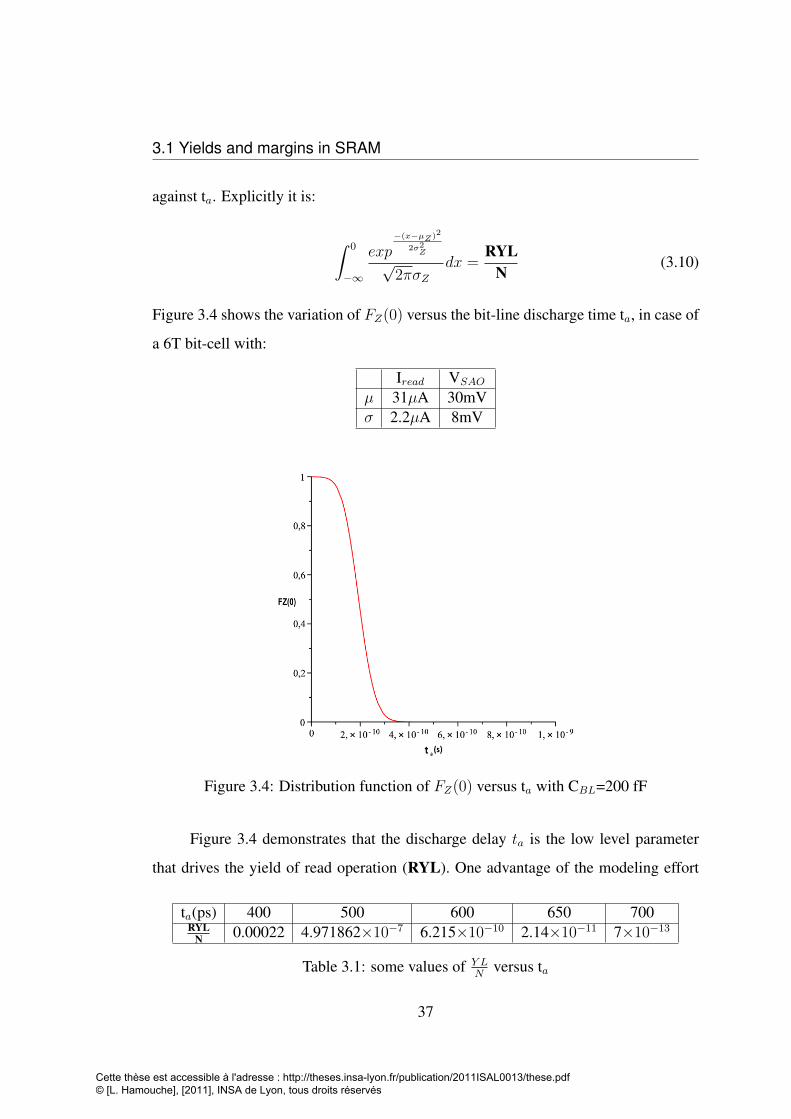
3.1 Yields and margins in SRAM
against ta. Explicitly it is:
∫ 0
−∞
exp−(x−µZ )2
2σ2Z
√2πσZ
dx =RYL
N(3.10)
Figure 3.4 shows the variation of FZ(0) versus the bit-line discharge time ta, in case of
a 6T bit-cell with:
Iread VSAO
µ 31µA 30mVσ 2.2µA 8mV
Figure 3.4: Distribution function of FZ(0) versus ta with CBL=200 fF
Figure 3.4 demonstrates that the discharge delay ta is the low level parameter
that drives the yield of read operation (RYL). One advantage of the modeling effort
ta(ps) 400 500 600 650 700RYL
N 0.00022 4.971862×10⁻⁷ 6.215×10⁻¹⁰ 2.14×10⁻¹¹ 7×10⁻¹³
Table 3.1: some values of Y LN
versus ta
37
Cette thèse est accessible à l'adresse : http://theses.insa-lyon.fr/publication/2011ISAL0013/these.pdf © [L. Hamouche], [2011], INSA de Lyon, tous droits réservés
3 Modeling for variability
presented here is to offer the determination of the critical parameters at the cell level
with respect to high level yields to guarantee. As presented in Table (3.1) Y LN
decrease
three decades after each 100ps of ta for an AQL=Y LN
=10−11, ta should be nearly equal
to 650ps more than that corresponds to an inflated values of RYL and penalize the
operation delay, but less corresponds to an unacceptable value of RYL . FZ shows
that RYL decrease violently so, according to the theoretical calculation made in this
section, the margin estimation can be made with a good precession.
3.2 Discussion on modeling results
In this section, results of theoretical calculation made in previously will be compared
with the result of Monte Carlo circuit simulations.
The 6T SRAM in figure 3.3 is designed in 32nm CMOS. The effect of various
discharge time values is evaluated with respect to read operation yield. The read oper-
ation is simulated selecting nominal values for the temperature and supply voltage. For
a given discharge time ta, 104 simulations are performed in the Monte Carlo scheme.
The read operation is considered as faulty when ∆VBL ≤ VSAO in the simulation re-
sults. The distribution of ∆VBL values is compared to the distribution of the offset in
the sense amplifier. The read operation yield is correlated to the overlapping of the
distributions. Practicaly one Monte Carlo run as in figure 3.5 costs nearly 5 min com-
putation on a computer farm. In order to satisfy a yield target, the designer must iterate
the Monte Carlo runs providing that he is taking action on an efficient circuit parameter
(delay margin ta with respect to read operation).
The modeling effort presented here wishes to give explicitely the circuit param-
eter value from the yield target value.
The Monte Carlo simulation results are plotted in figure 3.6 for increasing dis-
charge time values. The distributions of ∆VBL and VSAO do effectively move away. In
this case the read operation yield evoluates favorably. It appears that a discharge value
38
Cette thèse est accessible à l'adresse : http://theses.insa-lyon.fr/publication/2011ISAL0013/these.pdf © [L. Hamouche], [2011], INSA de Lyon, tous droits réservés
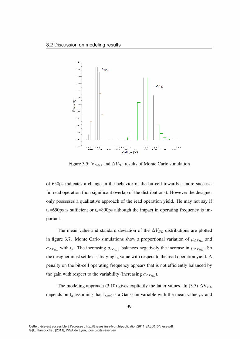
3.2 Discussion on modeling results
Figure 3.5: VSAO and ∆VBL results of Monte Carlo simulation
of 650ps indicates a change in the behavior of the bit-cell towards a more success-
ful read operation (non significant overlap of the distributions). However the designer
only possesses a qualitative approach of the read operation yield. He may not say if
ta=650ps is sufficient or ta=800ps although the impact in operating frequency is im-
portant.
The mean value and standard deviation of the ∆VBL distributions are plotted
in figure 3.7. Monte Carlo simulations show a proportional variation of µ∆VBL and
σ∆VBL with ta. The increasing σ∆VBL balances negatively the increase in µ∆VBL . So
the designer must settle a satisfying ta value with respect to the read operation yield. A
penalty on the bit-cell operating frequency appears that is not efficiently balanced by
the gain with respect to the variability (increasing σ∆VBL).
The modeling approach (3.10) gives explicitly the latter values. In (3.5) ∆VBL
depends on ta assuming that Iread is a Gaussian variable with the mean value µr and
39
Cette thèse est accessible à l'adresse : http://theses.insa-lyon.fr/publication/2011ISAL0013/these.pdf © [L. Hamouche], [2011], INSA de Lyon, tous droits réservés
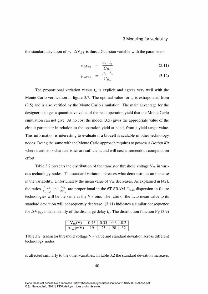
3 Modeling for variability
the standard deviation of σr. ∆VBL is thus a Gaussian variable with the parameters:
σ∆VBL =σr · taCBL
(3.11)
µ∆VBL =µr · taCBL
(3.12)
The proportional variation versus ta is explicit and agrees very well with the
Monte Carlo verification in figure 3.7. The optimal value for ta is extrapolated from
(3.5) and is also verified by the Monte Carlo simulation. The main advantage for the
designer is to get a quantitative value of the read operation yield that the Monte Carlo
simulation can not give. At no cost the model (3.5) gives the appropriate value of the
circuit parameter in relation to the operation yield at hand, from a yield target value.
This information is interesting to evaluate if a bit-cell is scalable in other technology
nodes. Doing the same with the Monte Carlo approach requires to possess a Design Kit
where transistors characteristics are sufficient, and will cost a tremendous computation
effort.
Table 3.2 presents the distribution of the transistor threshold voltage Vth in vari-
ous technology nodes. The standard variaton increases what demonstrates an increase
in the variability. Unfortunately the mean value of Vth decreases. As explained in [42],
the ratios IreadσIread
and VthσVth
are proportional in the 6T SRAM. Iread dispersion in future
technologies will be the same as the Vth one. The ratio of the Iread mean value to its
standard deviation will consequently decrease. (3.11) indicates a similar consequence
for ∆VBL, independently of the discharge delay ta. The distribution function FZ (3.9)
Vth(V) 0.45 0.35 0.3 0.2σVth(mV) 19 25 28 32
Table 3.2: transistor threshold voltage Vth value and standard deviation across differenttechnology nodes
is affected similarly to the other variables. In table 3.2 the standard deviation increases
40
Cette thèse est accessible à l'adresse : http://theses.insa-lyon.fr/publication/2011ISAL0013/these.pdf © [L. Hamouche], [2011], INSA de Lyon, tous droits réservés
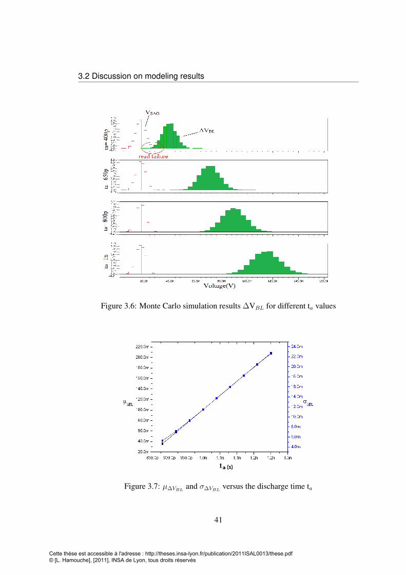
3.2 Discussion on modeling results
Figure 3.6: Monte Carlo simulation results ∆VBL for different ta values
Figure 3.7: µ∆VBL and σ∆VBL versus the discharge time ta
41
Cette thèse est accessible à l'adresse : http://theses.insa-lyon.fr/publication/2011ISAL0013/these.pdf © [L. Hamouche], [2011], INSA de Lyon, tous droits réservés
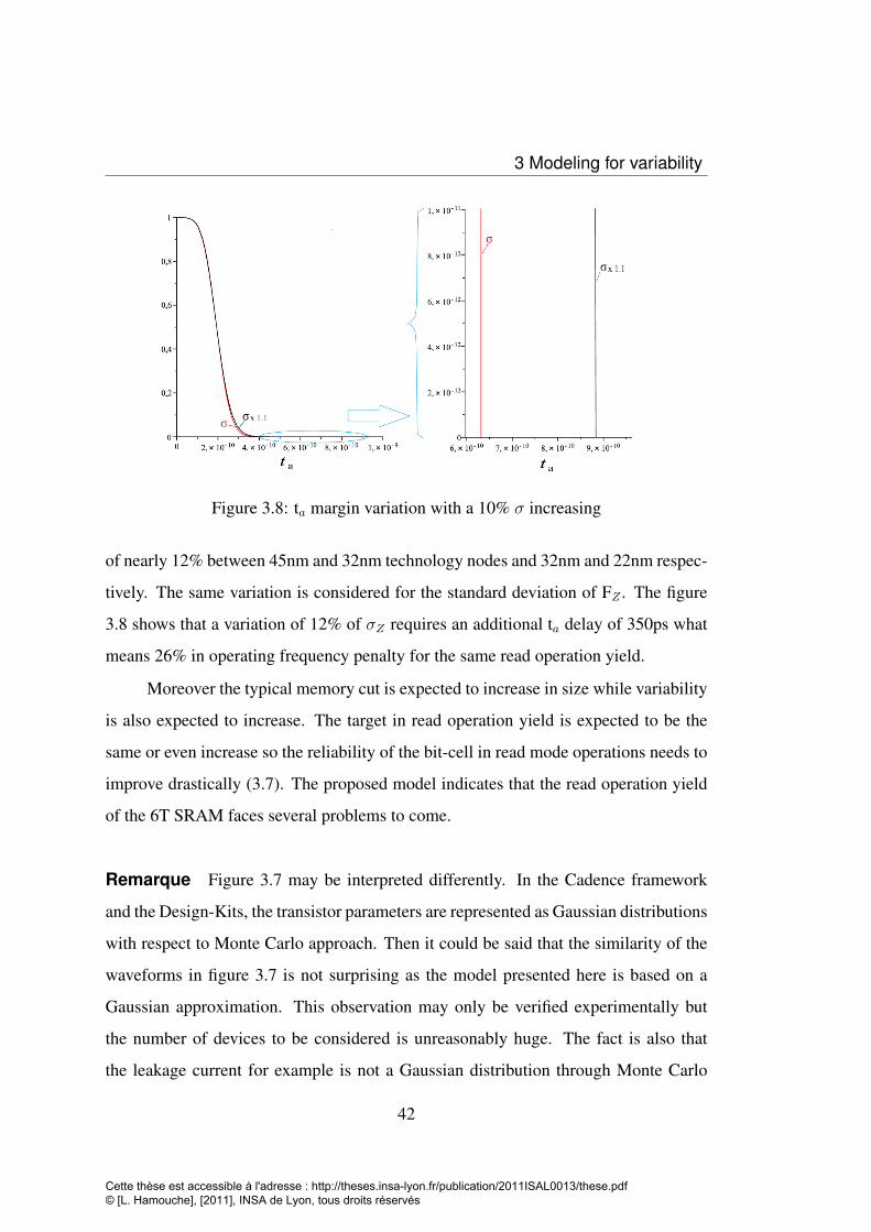
3 Modeling for variability
Figure 3.8: ta margin variation with a 10% σ increasing
of nearly 12% between 45nm and 32nm technology nodes and 32nm and 22nm respec-
tively. The same variation is considered for the standard deviation of FZ . The figure
3.8 shows that a variation of 12% of σZ requires an additional ta delay of 350ps what
means 26% in operating frequency penalty for the same read operation yield.
Moreover the typical memory cut is expected to increase in size while variability
is also expected to increase. The target in read operation yield is expected to be the
same or even increase so the reliability of the bit-cell in read mode operations needs to
improve drastically (3.7). The proposed model indicates that the read operation yield
of the 6T SRAM faces several problems to come.
Remarque Figure 3.7 may be interpreted differently. In the Cadence framework
and the Design-Kits, the transistor parameters are represented as Gaussian distributions
with respect to Monte Carlo approach. Then it could be said that the similarity of the
waveforms in figure 3.7 is not surprising as the model presented here is based on a
Gaussian approximation. This observation may only be verified experimentally but
the number of devices to be considered is unreasonably huge. The fact is also that
the leakage current for example is not a Gaussian distribution through Monte Carlo
42
Cette thèse est accessible à l'adresse : http://theses.insa-lyon.fr/publication/2011ISAL0013/these.pdf © [L. Hamouche], [2011], INSA de Lyon, tous droits réservés
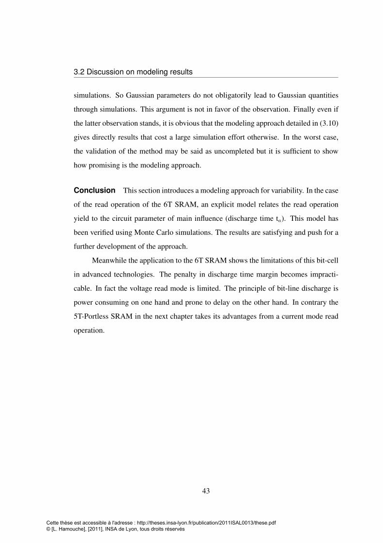
3.2 Discussion on modeling results
simulations. So Gaussian parameters do not obligatorily lead to Gaussian quantities
through simulations. This argument is not in favor of the observation. Finally even if
the latter observation stands, it is obvious that the modeling approach detailed in (3.10)
gives directly results that cost a large simulation effort otherwise. In the worst case,
the validation of the method may be said as uncompleted but it is sufficient to show
how promising is the modeling approach.
Conclusion This section introduces a modeling approach for variability. In the case
of the read operation of the 6T SRAM, an explicit model relates the read operation
yield to the circuit parameter of main influence (discharge time ta). This model has
been verified using Monte Carlo simulations. The results are satisfying and push for a
further development of the approach.
Meanwhile the application to the 6T SRAM shows the limitations of this bit-cell
in advanced technologies. The penalty in discharge time margin becomes impracti-
cable. In fact the voltage read mode is limited. The principle of bit-line discharge is
power consuming on one hand and prone to delay on the other hand. In contrary the
5T-Portless SRAM in the next chapter takes its advantages from a current mode read
operation.
43
Cette thèse est accessible à l'adresse : http://theses.insa-lyon.fr/publication/2011ISAL0013/these.pdf © [L. Hamouche], [2011], INSA de Lyon, tous droits réservés

44
Cette thèse est accessible à l'adresse : http://theses.insa-lyon.fr/publication/2011ISAL0013/these.pdf © [L. Hamouche], [2011], INSA de Lyon, tous droits réservés
4
PORTLESS BIT-CELL AND CURRENT
MODE OPERATION
4.1 5T SRAM bit-cells
There are two kinds of bit-cells with 5T transistors in literature: the 5T asymmetric
[43, 44] and the 5T Portless [45, 46, 47]. Figure 4.1 pictures both 5T SRAM bit-cells
with their respective butterfly curve. The 5T asymmetric bit-cell offers more density
than the 6T bit-cell and a better leakage current margin [43], but it requires a complex
periphery. Because of its single bit-line, the write ability and read stability trade-
off is difficult to obtain. The design of the 5T asymmetric requires thus an additional
periphery to assist the read and/or write operation [44]. The dynamic hopping of supply
voltage is the efficient lever to solve the read/write antagonist assistance. It renders
the memory peripheral more complex than for the 6T. It reduces the possible gain in
density with the missing transistor. This added overhead and the relatively limited
benefits have prevented the widespread use of asymmetric 5T cells. Moreover the 5T
asymmetric has been demonstrated in 45nm but not in 32 nm.
The 5T-Portless remains the alternative bit-cell to the 6T bit-cell for low-power
and always-on applications. The Pass-Gate transistors are missing in the Portless bit-
cell but replaced by a transistor (AXS) connected to the two bit-cell internal nodes.
45
Cette thèse est accessible à l'adresse : http://theses.insa-lyon.fr/publication/2011ISAL0013/these.pdf © [L. Hamouche], [2011], INSA de Lyon, tous droits réservés
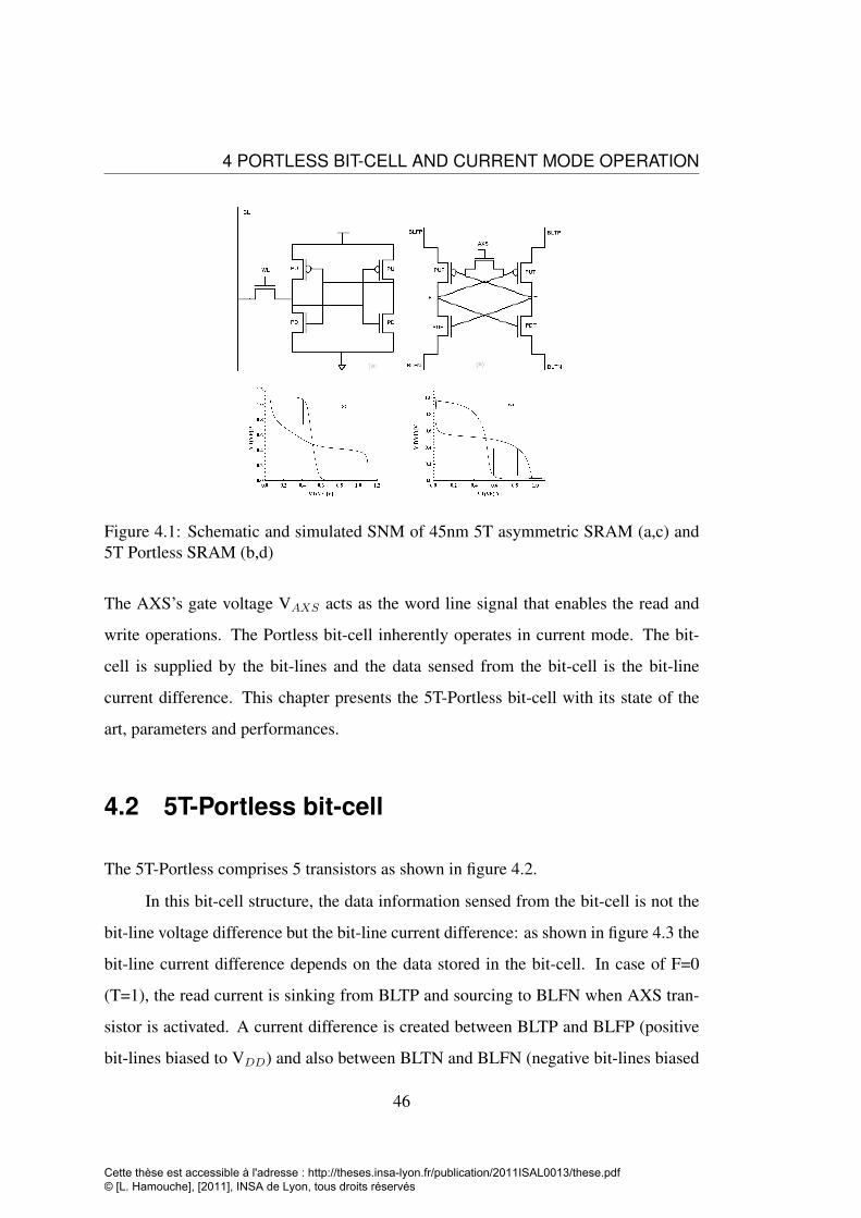
4 PORTLESS BIT-CELL AND CURRENT MODE OPERATION
Figure 4.1: Schematic and simulated SNM of 45nm 5T asymmetric SRAM (a,c) and5T Portless SRAM (b,d)
The AXS’s gate voltage VAXS acts as the word line signal that enables the read and
write operations. The Portless bit-cell inherently operates in current mode. The bit-
cell is supplied by the bit-lines and the data sensed from the bit-cell is the bit-line
current difference. This chapter presents the 5T-Portless bit-cell with its state of the
art, parameters and performances.
4.2 5T-Portless bit-cell
The 5T-Portless comprises 5 transistors as shown in figure 4.2.
In this bit-cell structure, the data information sensed from the bit-cell is not the
bit-line voltage difference but the bit-line current difference: as shown in figure 4.3 the
bit-line current difference depends on the data stored in the bit-cell. In case of F=0
(T=1), the read current is sinking from BLTP and sourcing to BLFN when AXS tran-
sistor is activated. A current difference is created between BLTP and BLFP (positive
bit-lines biased to VDD) and also between BLTN and BLFN (negative bit-lines biased
46
Cette thèse est accessible à l'adresse : http://theses.insa-lyon.fr/publication/2011ISAL0013/these.pdf © [L. Hamouche], [2011], INSA de Lyon, tous droits réservés
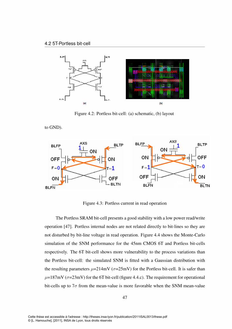
4.2 5T-Portless bit-cell
Figure 4.2: Portless bit-cell: (a) schematic, (b) layout
to GND).
Figure 4.3: Portless current in read operation
The Portless SRAM bit-cell presents a good stability with a low power read/write
operation [47]. Portless internal nodes are not related directly to bit-lines so they are
not disturbed by bit-line voltage in read operation. Figure 4.4 shows the Monte-Carlo
simulation of the SNM performance for the 45nm CMOS 6T and Portless bit-cells
respectively. The 6T bit-cell shows more vulnerability to the process variations than
the Portless bit-cell: the simulated SNM is fitted with a Gaussian distribution with
the resulting parameters µ=214mV (σ=25mV) for the Portless bit-cell. It is safer than
µ=187mV (σ=23mV) for the 6T bit-cell (figure 4.4.c). The requirement for operational
bit-cells up to 7σ from the mean-value is more favorable when the SNM mean-value
47
Cette thèse est accessible à l'adresse : http://theses.insa-lyon.fr/publication/2011ISAL0013/these.pdf © [L. Hamouche], [2011], INSA de Lyon, tous droits réservés
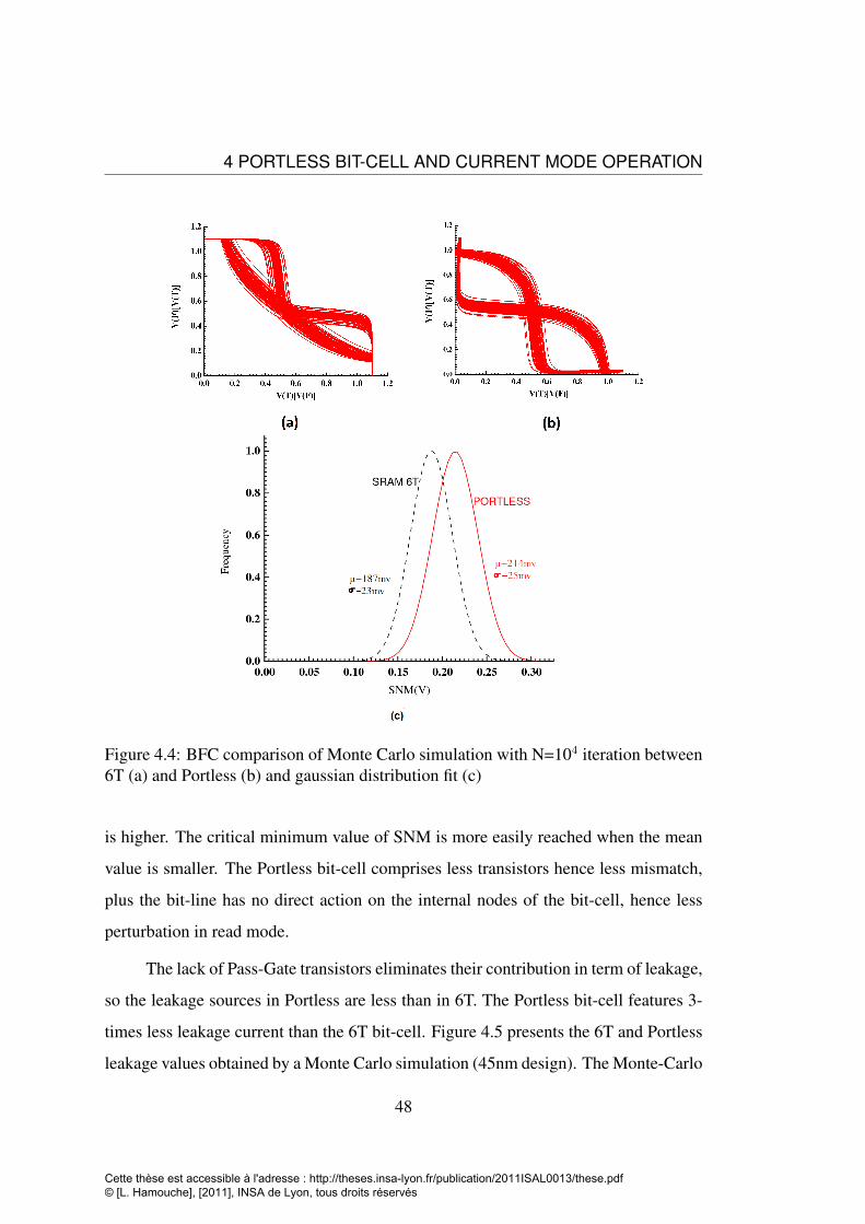
4 PORTLESS BIT-CELL AND CURRENT MODE OPERATION
Figure 4.4: BFC comparison of Monte Carlo simulation with N=104 iteration between6T (a) and Portless (b) and gaussian distribution fit (c)
is higher. The critical minimum value of SNM is more easily reached when the mean
value is smaller. The Portless bit-cell comprises less transistors hence less mismatch,
plus the bit-line has no direct action on the internal nodes of the bit-cell, hence less
perturbation in read mode.
The lack of Pass-Gate transistors eliminates their contribution in term of leakage,
so the leakage sources in Portless are less than in 6T. The Portless bit-cell features 3-
times less leakage current than the 6T bit-cell. Figure 4.5 presents the 6T and Portless
leakage values obtained by a Monte Carlo simulation (45nm design). The Monte-Carlo
48
Cette thèse est accessible à l'adresse : http://theses.insa-lyon.fr/publication/2011ISAL0013/these.pdf © [L. Hamouche], [2011], INSA de Lyon, tous droits réservés
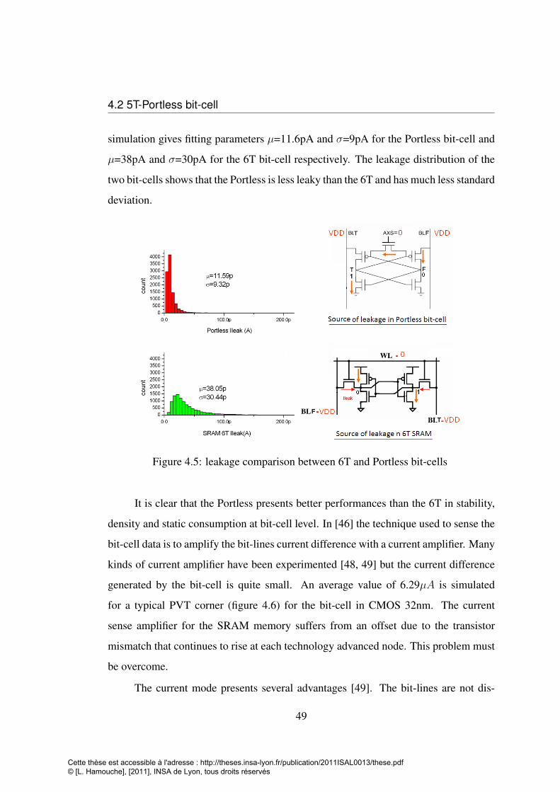
4.2 5T-Portless bit-cell
simulation gives fitting parameters µ=11.6pA and σ=9pA for the Portless bit-cell and
µ=38pA and σ=30pA for the 6T bit-cell respectively. The leakage distribution of the
two bit-cells shows that the Portless is less leaky than the 6T and has much less standard
deviation.
Figure 4.5: leakage comparison between 6T and Portless bit-cells
It is clear that the Portless presents better performances than the 6T in stability,
density and static consumption at bit-cell level. In [46] the technique used to sense the
bit-cell data is to amplify the bit-lines current difference with a current amplifier. Many
kinds of current amplifier have been experimented [48, 49] but the current difference
generated by the bit-cell is quite small. An average value of 6.29µA is simulated
for a typical PVT corner (figure 4.6) for the bit-cell in CMOS 32nm. The current
sense amplifier for the SRAM memory suffers from an offset due to the transistor
mismatch that continues to rise at each technology advanced node. This problem must
be overcome.
The current mode presents several advantages [49]. The bit-lines are not dis-
49
Cette thèse est accessible à l'adresse : http://theses.insa-lyon.fr/publication/2011ISAL0013/these.pdf © [L. Hamouche], [2011], INSA de Lyon, tous droits réservés
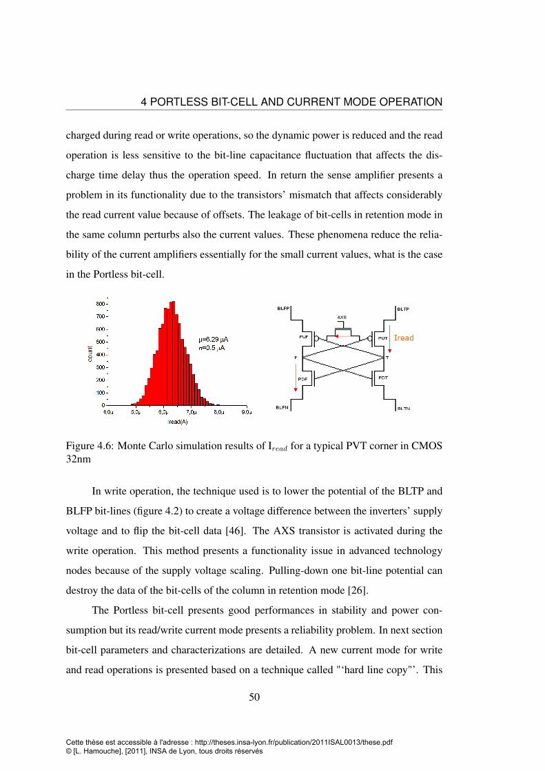
4 PORTLESS BIT-CELL AND CURRENT MODE OPERATION
charged during read or write operations, so the dynamic power is reduced and the read
operation is less sensitive to the bit-line capacitance fluctuation that affects the dis-
charge time delay thus the operation speed. In return the sense amplifier presents a
problem in its functionality due to the transistors’ mismatch that affects considerably
the read current value because of offsets. The leakage of bit-cells in retention mode in
the same column perturbs also the current values. These phenomena reduce the relia-
bility of the current amplifiers essentially for the small current values, what is the case
in the Portless bit-cell.
Figure 4.6: Monte Carlo simulation results of Iread for a typical PVT corner in CMOS32nm
In write operation, the technique used is to lower the potential of the BLTP and
BLFP bit-lines (figure 4.2) to create a voltage difference between the inverters’ supply
voltage and to flip the bit-cell data [46]. The AXS transistor is activated during the
write operation. This method presents a functionality issue in advanced technology
nodes because of the supply voltage scaling. Pulling-down one bit-line potential can
destroy the data of the bit-cells of the column in retention mode [26].
The Portless bit-cell presents good performances in stability and power con-
sumption but its read/write current mode presents a reliability problem. In next section
bit-cell parameters and characterizations are detailed. A new current mode for write
and read operations is presented based on a technique called "‘hard line copy"’. This
50
Cette thèse est accessible à l'adresse : http://theses.insa-lyon.fr/publication/2011ISAL0013/these.pdf © [L. Hamouche], [2011], INSA de Lyon, tous droits réservés
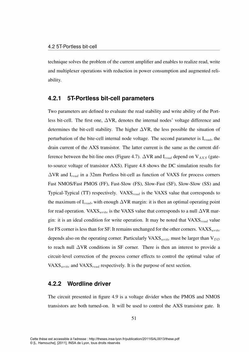
4.2 5T-Portless bit-cell
technique solves the problem of the current amplifier and enables to realize read, write
and multiplexer operations with reduction in power consumption and augmented reli-
ability.
4.2.1 5T-Portless bit-cell parameters
Two parameters are defined to evaluate the read stability and write ability of the Port-
less bit-cell. The first one, ∆VR, denotes the internal nodes’ voltage difference and
determines the bit-cell stability. The higher ∆VR, the less possible the situation of
perturbation of the bite-cell internal node voltage. The second parameter is Iread, the
drain current of the AXS transistor. The latter current is the same as the current dif-
ference between the bit-line ones (Figure 4.7). ∆VR and Iread depend on VAXS (gate-
to-source voltage of transistor AXS). Figure 4.8 shows the DC simulation results for
∆VR and Iread in a 32nm Portless bit-cell as function of VAXS for process corners
Fast NMOS/Fast PMOS (FF), Fast-Slow (FS), Slow-Fast (SF), Slow-Slow (SS) and
Typical-Typical (TT) respectively. VAXSread is the VAXS value that corresponds to
the maximum of Iread, with enough ∆VR margin: it is then an optimal operating point
for read operation. VAXSwrite is the VAXS value that corresponds to a null ∆VR mar-
gin: it is an ideal condition for write operation. It may be noted that VAXSread value
for FS corner is less than for SF. It remains unchanged for the other corners. VAXSwrite
depends also on the operating corner. Particularly VAXSwrite must be larger than VDD
to reach null ∆VR conditions in SF corner. There is then an interest to provide a
circuit-level correction of the process corner effects to control the optimal value of
VAXSwrite and VAXSread respectively. It is the purpose of next section.
4.2.2 Wordline driver
The circuit presented in figure 4.9 is a voltage divider when the PMOS and NMOS
transistors are both turned-on. It will be used to control the AXS transistor gate. It
51
Cette thèse est accessible à l'adresse : http://theses.insa-lyon.fr/publication/2011ISAL0013/these.pdf © [L. Hamouche], [2011], INSA de Lyon, tous droits réservés
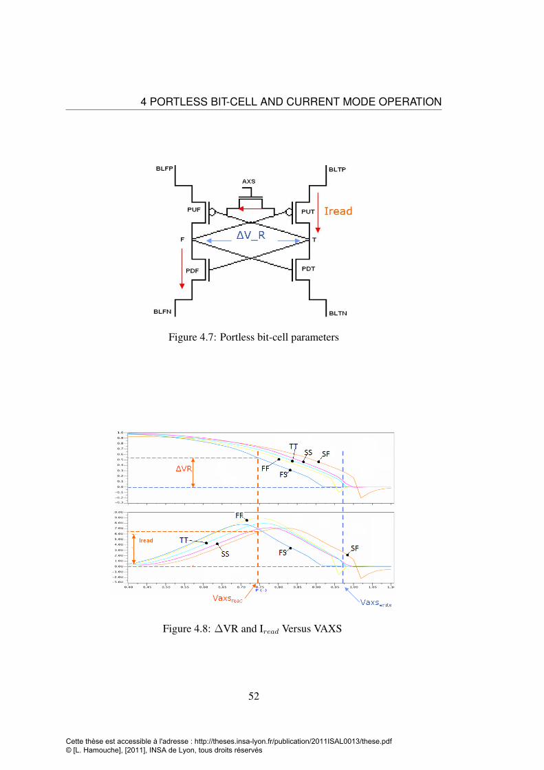
4 PORTLESS BIT-CELL AND CURRENT MODE OPERATION
Figure 4.7: Portless bit-cell parameters
Figure 4.8: ∆VR and Iread Versus VAXS
52
Cette thèse est accessible à l'adresse : http://theses.insa-lyon.fr/publication/2011ISAL0013/these.pdf © [L. Hamouche], [2011], INSA de Lyon, tous droits réservés
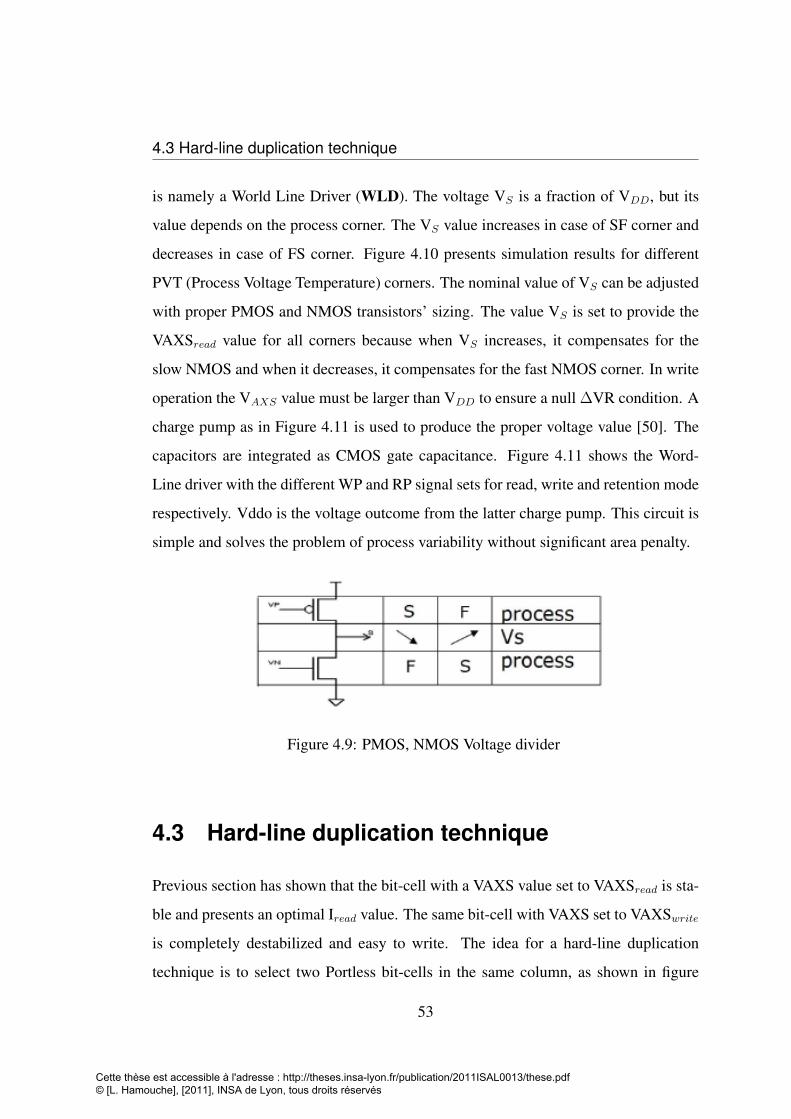
4.3 Hard-line duplication technique
is namely a World Line Driver (WLD). The voltage VS is a fraction of VDD, but its
value depends on the process corner. The VS value increases in case of SF corner and
decreases in case of FS corner. Figure 4.10 presents simulation results for different
PVT (Process Voltage Temperature) corners. The nominal value of VS can be adjusted
with proper PMOS and NMOS transistors’ sizing. The value VS is set to provide the
VAXSread value for all corners because when VS increases, it compensates for the
slow NMOS and when it decreases, it compensates for the fast NMOS corner. In write
operation the VAXS value must be larger than VDD to ensure a null ∆VR condition. A
charge pump as in Figure 4.11 is used to produce the proper voltage value [50]. The
capacitors are integrated as CMOS gate capacitance. Figure 4.11 shows the Word-
Line driver with the different WP and RP signal sets for read, write and retention mode
respectively. Vddo is the voltage outcome from the latter charge pump. This circuit is
simple and solves the problem of process variability without significant area penalty.
Figure 4.9: PMOS, NMOS Voltage divider
4.3 Hard-line duplication technique
Previous section has shown that the bit-cell with a VAXS value set to VAXSread is sta-
ble and presents an optimal Iread value. The same bit-cell with VAXS set to VAXSwrite
is completely destabilized and easy to write. The idea for a hard-line duplication
technique is to select two Portless bit-cells in the same column, as shown in figure
53
Cette thèse est accessible à l'adresse : http://theses.insa-lyon.fr/publication/2011ISAL0013/these.pdf © [L. Hamouche], [2011], INSA de Lyon, tous droits réservés
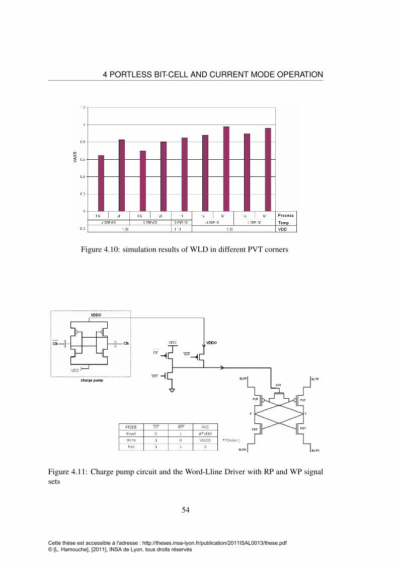
4 PORTLESS BIT-CELL AND CURRENT MODE OPERATION
Figure 4.10: simulation results of WLD in different PVT corners
Figure 4.11: Charge pump circuit and the Word-Lline Driver with RP and WP signalsets
54
Cette thèse est accessible à l'adresse : http://theses.insa-lyon.fr/publication/2011ISAL0013/these.pdf © [L. Hamouche], [2011], INSA de Lyon, tous droits réservés
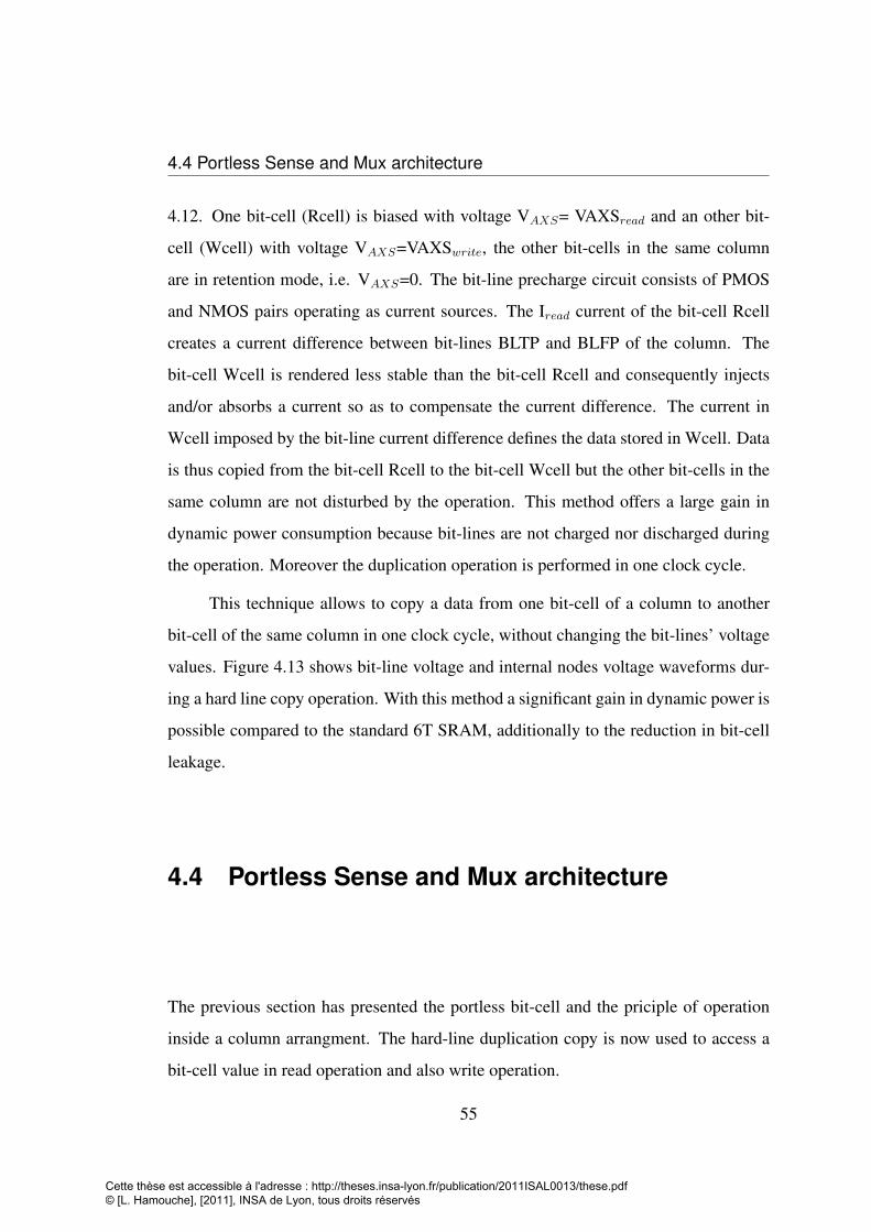
4.4 Portless Sense and Mux architecture
4.12. One bit-cell (Rcell) is biased with voltage VAXS= VAXSread and an other bit-
cell (Wcell) with voltage VAXS=VAXSwrite, the other bit-cells in the same column
are in retention mode, i.e. VAXS=0. The bit-line precharge circuit consists of PMOS
and NMOS pairs operating as current sources. The Iread current of the bit-cell Rcell
creates a current difference between bit-lines BLTP and BLFP of the column. The
bit-cell Wcell is rendered less stable than the bit-cell Rcell and consequently injects
and/or absorbs a current so as to compensate the current difference. The current in
Wcell imposed by the bit-line current difference defines the data stored in Wcell. Data
is thus copied from the bit-cell Rcell to the bit-cell Wcell but the other bit-cells in the
same column are not disturbed by the operation. This method offers a large gain in
dynamic power consumption because bit-lines are not charged nor discharged during
the operation. Moreover the duplication operation is performed in one clock cycle.
This technique allows to copy a data from one bit-cell of a column to another
bit-cell of the same column in one clock cycle, without changing the bit-lines’ voltage
values. Figure 4.13 shows bit-line voltage and internal nodes voltage waveforms dur-
ing a hard line copy operation. With this method a significant gain in dynamic power is
possible compared to the standard 6T SRAM, additionally to the reduction in bit-cell
leakage.
4.4 Portless Sense and Mux architecture
The previous section has presented the portless bit-cell and the priciple of operation
inside a column arrangment. The hard-line duplication copy is now used to access a
bit-cell value in read operation and also write operation.
55
Cette thèse est accessible à l'adresse : http://theses.insa-lyon.fr/publication/2011ISAL0013/these.pdf © [L. Hamouche], [2011], INSA de Lyon, tous droits réservés
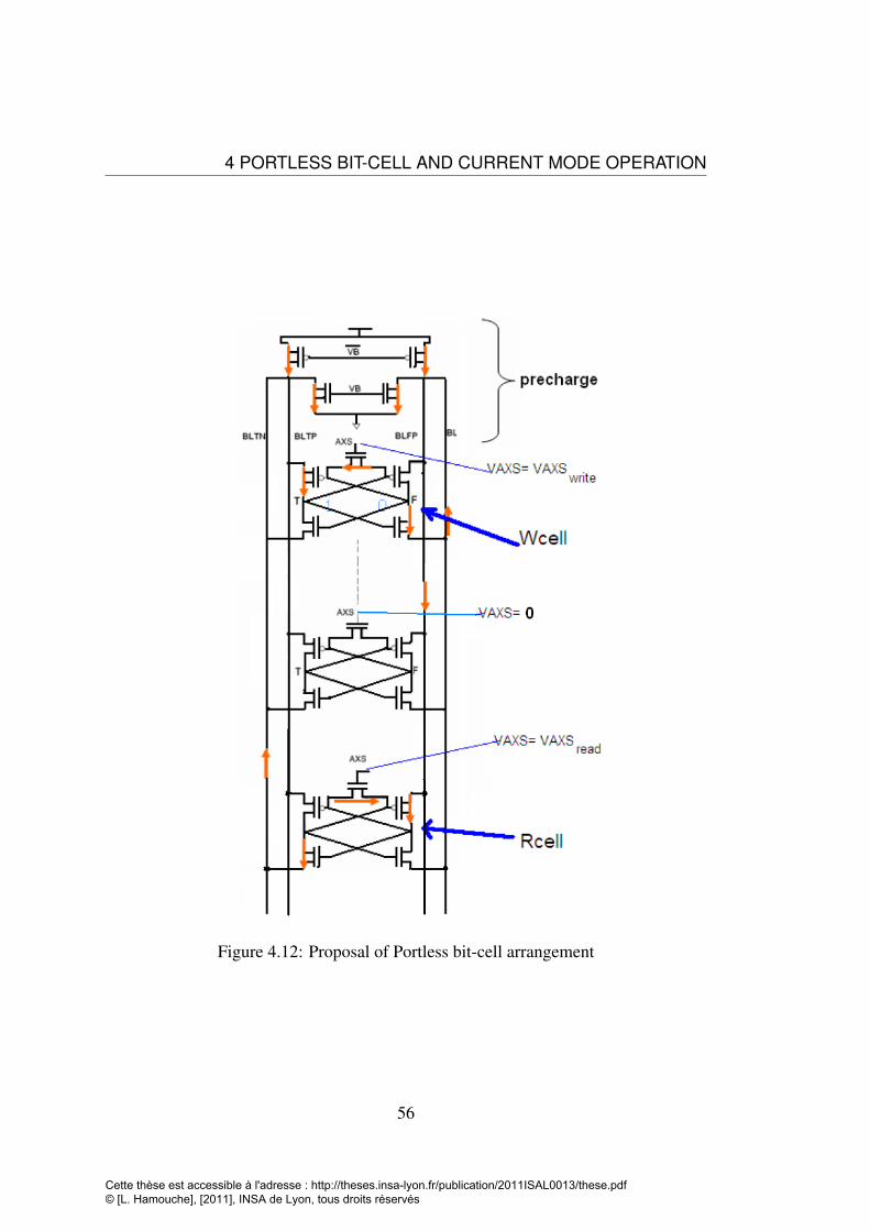
4 PORTLESS BIT-CELL AND CURRENT MODE OPERATION
Figure 4.12: Proposal of Portless bit-cell arrangement
56
Cette thèse est accessible à l'adresse : http://theses.insa-lyon.fr/publication/2011ISAL0013/these.pdf © [L. Hamouche], [2011], INSA de Lyon, tous droits réservés
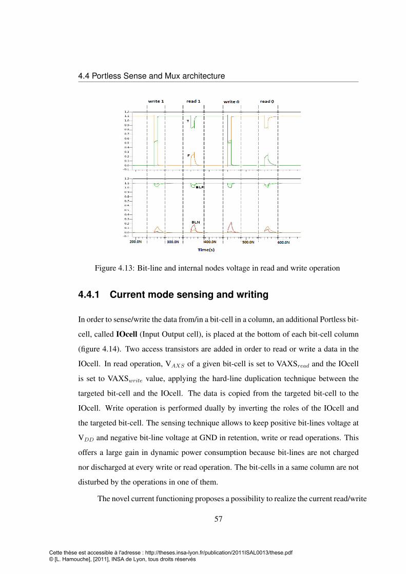
4.4 Portless Sense and Mux architecture
Figure 4.13: Bit-line and internal nodes voltage in read and write operation
4.4.1 Current mode sensing and writing
In order to sense/write the data from/in a bit-cell in a column, an additional Portless bit-
cell, called IOcell (Input Output cell), is placed at the bottom of each bit-cell column
(figure 4.14). Two access transistors are added in order to read or write a data in the
IOcell. In read operation, VAXS of a given bit-cell is set to VAXSread and the IOcell
is set to VAXSwrite value, applying the hard-line duplication technique between the
targeted bit-cell and the IOcell. The data is copied from the targeted bit-cell to the
IOcell. Write operation is performed dually by inverting the roles of the IOcell and
the targeted bit-cell. The sensing technique allows to keep positive bit-lines voltage at
VDD and negative bit-line voltage at GND in retention, write or read operations. This
offers a large gain in dynamic power consumption because bit-lines are not charged
nor discharged at every write or read operation. The bit-cells in a same column are not
disturbed by the operations in one of them.
The novel current functioning proposes a possibility to realize the current read/write
57
Cette thèse est accessible à l'adresse : http://theses.insa-lyon.fr/publication/2011ISAL0013/these.pdf © [L. Hamouche], [2011], INSA de Lyon, tous droits réservés
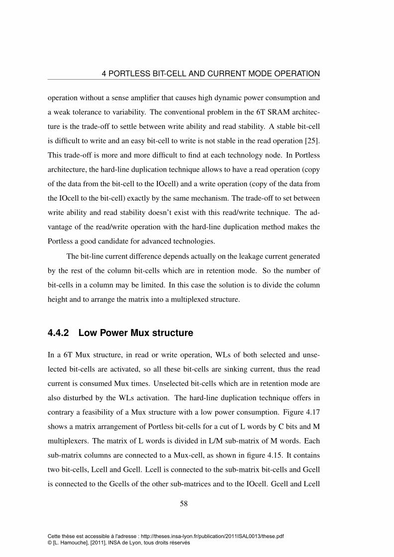
4 PORTLESS BIT-CELL AND CURRENT MODE OPERATION
operation without a sense amplifier that causes high dynamic power consumption and
a weak tolerance to variability. The conventional problem in the 6T SRAM architec-
ture is the trade-off to settle between write ability and read stability. A stable bit-cell
is difficult to write and an easy bit-cell to write is not stable in the read operation [25].
This trade-off is more and more difficult to find at each technology node. In Portless
architecture, the hard-line duplication technique allows to have a read operation (copy
of the data from the bit-cell to the IOcell) and a write operation (copy of the data from
the IOcell to the bit-cell) exactly by the same mechanism. The trade-off to set between
write ability and read stability doesn’t exist with this read/write technique. The ad-
vantage of the read/write operation with the hard-line duplication method makes the
Portless a good candidate for advanced technologies.
The bit-line current difference depends actually on the leakage current generated
by the rest of the column bit-cells which are in retention mode. So the number of
bit-cells in a column may be limited. In this case the solution is to divide the column
height and to arrange the matrix into a multiplexed structure.
4.4.2 Low Power Mux structure
In a 6T Mux structure, in read or write operation, WLs of both selected and unse-
lected bit-cells are activated, so all these bit-cells are sinking current, thus the read
current is consumed Mux times. Unselected bit-cells which are in retention mode are
also disturbed by the WLs activation. The hard-line duplication technique offers in
contrary a feasibility of a Mux structure with a low power consumption. Figure 4.17
shows a matrix arrangement of Portless bit-cells for a cut of L words by C bits and M
multiplexers. The matrix of L words is divided in L/M sub-matrix of M words. Each
sub-matrix columns are connected to a Mux-cell, as shown in figure 4.15. It contains
two bit-cells, Lcell and Gcell. Lcell is connected to the sub-matrix bit-cells and Gcell
is connected to the Gcells of the other sub-matrices and to the IOcell. Gcell and Lcell
58
Cette thèse est accessible à l'adresse : http://theses.insa-lyon.fr/publication/2011ISAL0013/these.pdf © [L. Hamouche], [2011], INSA de Lyon, tous droits réservés
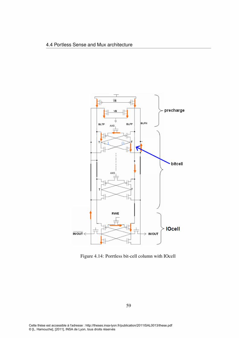
4.4 Portless Sense and Mux architecture
Figure 4.14: Porrtless bit-cell column with IOcell
59
Cette thèse est accessible à l'adresse : http://theses.insa-lyon.fr/publication/2011ISAL0013/these.pdf © [L. Hamouche], [2011], INSA de Lyon, tous droits réservés
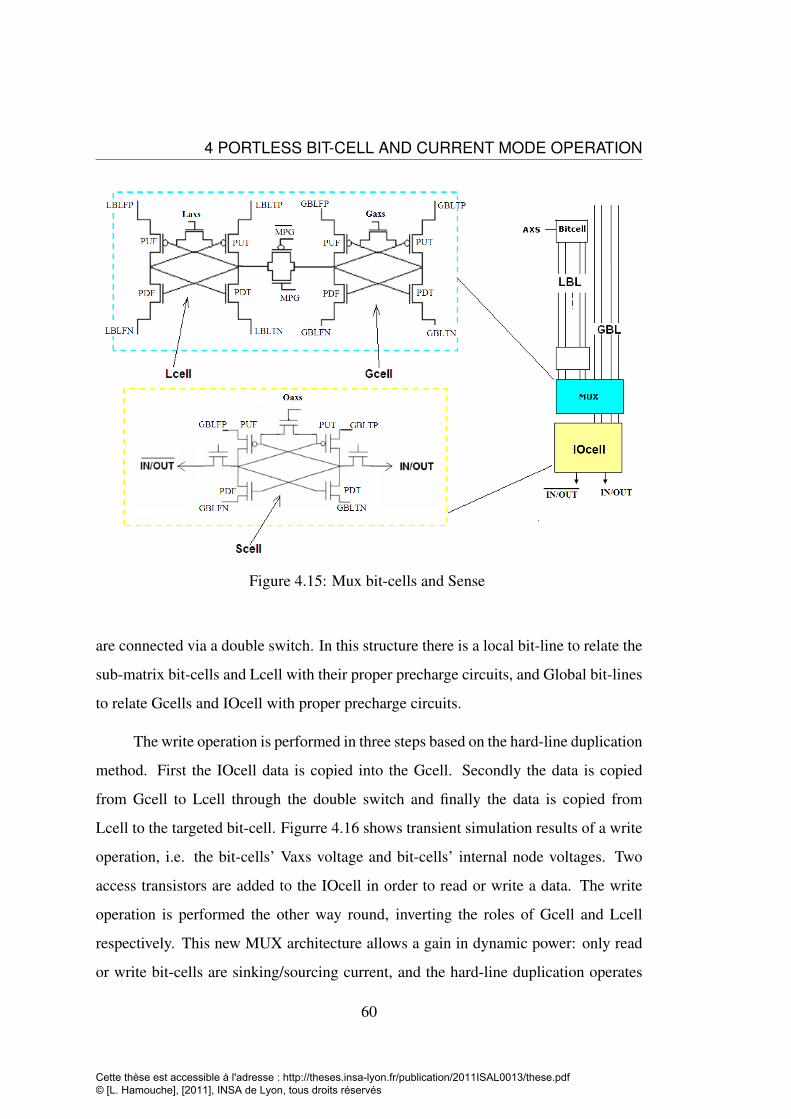
4 PORTLESS BIT-CELL AND CURRENT MODE OPERATION
Figure 4.15: Mux bit-cells and Sense
are connected via a double switch. In this structure there is a local bit-line to relate the
sub-matrix bit-cells and Lcell with their proper precharge circuits, and Global bit-lines
to relate Gcells and IOcell with proper precharge circuits.
The write operation is performed in three steps based on the hard-line duplication
method. First the IOcell data is copied into the Gcell. Secondly the data is copied
from Gcell to Lcell through the double switch and finally the data is copied from
Lcell to the targeted bit-cell. Figurre 4.16 shows transient simulation results of a write
operation, i.e. the bit-cells’ Vaxs voltage and bit-cells’ internal node voltages. Two
access transistors are added to the IOcell in order to read or write a data. The write
operation is performed the other way round, inverting the roles of Gcell and Lcell
respectively. This new MUX architecture allows a gain in dynamic power: only read
or write bit-cells are sinking/sourcing current, and the hard-line duplication operates
60
Cette thèse est accessible à l'adresse : http://theses.insa-lyon.fr/publication/2011ISAL0013/these.pdf © [L. Hamouche], [2011], INSA de Lyon, tous droits réservés
4.4 Portless Sense and Mux architecture
without charge nor discharge of bit-lines. Bit-cells in retention are not disturbed and
may even be in retention mode under low VDD condition to reduce leakage [26].
Figure 4.16: Vaxs and cells’ internal node voltages during a write operation in aCMOS32nm Portless arrangement
This chapter has introduced the 5T Portless SRAM as a good candidate for low-
power, always-on memory. The classical voltage sense has come to a limit as demon-
strated in literature. The use of current sense amplifiers does not solve the limitations.
The hard-line duplication has been developed and overcomes the limitations. The 5T-
Portless also operates with new conditions that give new interests in the Portless in
advanced technology nodes. The leakage issue is naturally minor because of the 5T
structure. The dynamic power consumption is controlled through a multiplexed ar-
rangement of bit-cells and an original implementation of the hard-line copy technique.
Next chapter introduces the design and simulations in CMOS 32nm.
61
Cette thèse est accessible à l'adresse : http://theses.insa-lyon.fr/publication/2011ISAL0013/these.pdf © [L. Hamouche], [2011], INSA de Lyon, tous droits réservés
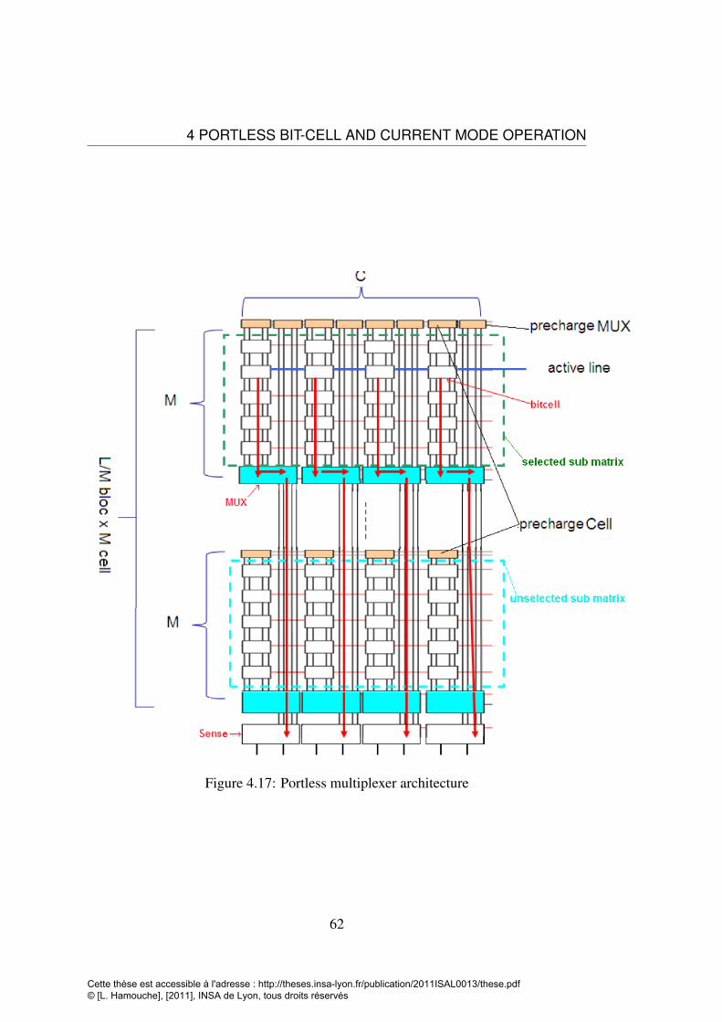
4 PORTLESS BIT-CELL AND CURRENT MODE OPERATION
Figure 4.17: Portless multiplexer architecture
62
Cette thèse est accessible à l'adresse : http://theses.insa-lyon.fr/publication/2011ISAL0013/these.pdf © [L. Hamouche], [2011], INSA de Lyon, tous droits réservés
5
Test chip and simulation results
The original structure of the 5T-Portless memory based on the hard line-duplication
technique is implemented in CMOS 32nm. A cut of 64Kb (1024×64) is developed in
this technology. Figure 5.1 shows the structure of the cut. The matrix of 1024x64 is
divided into 32 sub-matrixes of 32x64 bits. The Multiplexer architecture detailed in
Chapter 4 is implemented here. The WLD block is the word line driver that generates
the VAXS voltage potential level. A charge pump is placed in each sub-matrix to
control the Vddo level for the WLD block. The Control block controls the read and
the write operations and the retention mode. It generates the pulse for different signals
(AXS, Gaxs, Laxs, Oaxs . . .). This block is repeated for each sub-matrix to reduce
the power consumption by limitation of wires’ length. Dummy is a fictitious line of
cells that gives a feedback about the process status to set up the control signals. Finally
the Decoder blocks select the active sub-matrix (MSB ) and the sub-matrix’ active
line (LSB ). A technique of predecoding is implemented to reduce the dynamic power
consumption.
In this chapter the design of the memory cut is detailed. Simulation results and a
benchmark with the conventional 6T architecture is discussed.
63
Cette thèse est accessible à l'adresse : http://theses.insa-lyon.fr/publication/2011ISAL0013/these.pdf © [L. Hamouche], [2011], INSA de Lyon, tous droits réservés
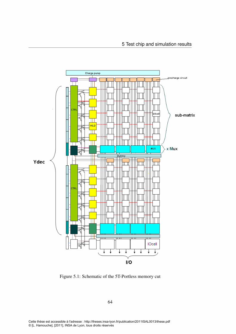
5 Test chip and simulation results
Figure 5.1: Schematic of the 5T-Portless memory cut
64
Cette thèse est accessible à l'adresse : http://theses.insa-lyon.fr/publication/2011ISAL0013/these.pdf © [L. Hamouche], [2011], INSA de Lyon, tous droits réservés
5.1 Test chip design
Supply Voltage (VDD) 0.9V, 1V, 1.1Vtemperature -40◦C, +25◦C, +125 ◦C
process corner FF, FS, SF, SS, TT
Table 5.1: Testchip PVT Specification
5.1 Test chip design
The different blocks required to apply the hard line duplication are presented. The
technique of hard line duplication is implemented to ensure the read and write oper-
ations and activates the multiplexed structure. The design is implemented with the
CMOS32lp (low power) RVT (regular Vth) process. The gate length is extended to
40nm to have a positive impact on the leakage and variability issues. As explained in
(2.1), the increase in L and W concurs to a reduction in Vth hence on bit-cell perfor-
mance with respect to variability. The test chip must be functional with the following
specifications:
Simulations are performed with the "Eldo" simulator for the small blocks and
with the simulator "xa" (fast spice simulator) for the full cut. All simulations in this
chapter are performed with extracted netlists that include the parasitic devices in lay-
out.
5.1.1 Bit-cell to matrix array
The 5T-Portless, as explained in Chapter 4, is a cross-coupled inverter with an AXS
transistor. The AXS’ drain and source are connected to the bit-cell internal nodes.
The bit-cell is supplied by its four bit-lines: BLTP and BLFP (connected to VDD
potential voltage) and BLTN and BLFN (connected to the GND potential voltage).
The five bit-cell transistors are sized to W=240nm and length L=40nm. The bit-cell
size is 0.444µm×0.864µm=0.383µm2. The eSRAM is designed with the standard
Design Kit, i.e. without the SRAM implants that allow the violation of DRC (Design
65
Cette thèse est accessible à l'adresse : http://theses.insa-lyon.fr/publication/2011ISAL0013/these.pdf © [L. Hamouche], [2011], INSA de Lyon, tous droits réservés
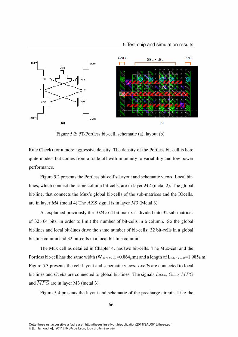
5 Test chip and simulation results
Figure 5.2: 5T-Portless bit-cell, schematic (a), layout (b)
Rule Check) for a more aggressive density. The density of the Portless bit-cell is here
quite modest but comes from a trade-off with immunity to variability and low power
performance.
Figure 5.2 presents the Portless bit-cell’s Layout and schematic views. Local bit-
lines, which connect the same column bit-cells, are in layer M2 (metal 2). The global
bit-line, that connects the Mux’s global bit-cells of the sub-matrices and the IOcells,
are in layer M4 (metal 4).The AXS signal is in layer M3 (Metal 3).
As explained previously the 1024×64 bit matrix is divided into 32 sub-matrices
of 32×64 bits, in order to limit the number of bit-cells in a column. So the global
bit-lines and local bit-lines drive the same number of bit-cells: 32 bit-cells in a global
bit-line column and 32 bit-cells in a local bit-line column.
The Mux cell as detailed in Chapter 4, has two bit-cells. The Mux-cell and the
Portless bit-cell has the same width (WMUXcell=0.864µm) and a length of LMUXcell=1.985µm.
Figure 5.3 presents the cell layout and schematic views. Lcells are connected to local
bit-lines and Gcells are connected to global bit-lines. The signals Laxs, Gaxs MPG
and MPG are in layer M3 (metal 3).
Figure 5.4 presents the layout and schematic of the precharge circuit. Like the
66
Cette thèse est accessible à l'adresse : http://theses.insa-lyon.fr/publication/2011ISAL0013/these.pdf © [L. Hamouche], [2011], INSA de Lyon, tous droits réservés
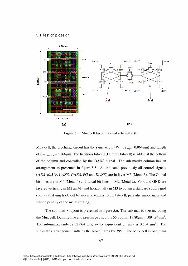
5.1 Test chip design
Figure 5.3: Mux cell layout (a) and schematic (b)
Mux cell, the precharge circuit has the same width (WPrecharge=0.864µm) and length
of LPrecharge=3.166µm. The fictitious bit-cell (Dummy bit-cell) is added at the bottom
of the column and controlled by the DAXS signal. The sub-matrix column has an
arrangement as presented in figure 5.5. As indicated previously all control signals
(AXS <0:31>, LAXS, GAXS, PG and DAXS ) are in layer M3 (Metal 3). The Global
bit-lines are in M4 (Metal 4) and Local bit-lines in M2 (Metal 2). VDD and GND are
layered vertically in M2 an M4 and horizontally in M3 to obtain a standard supply grid
(i.e. a satisfying trade-off between proximity to the bit-cell, parasitic impedances and
silicon penalty of the metal routing).
The sub-matrix layout is presented in figure 5.6. The sub-matrix size including
the Mux cell, Dummy line and precharge circuit is 55.30µm×19.80µm= 1094.94µm2.
The sub-matrix embeds 32×64 bits, so the equivalent bit area is 0.534 µm2. The
sub-matrix arrangement inflates the bit-cell area by 39%. The Mux cell is one main
67
Cette thèse est accessible à l'adresse : http://theses.insa-lyon.fr/publication/2011ISAL0013/these.pdf © [L. Hamouche], [2011], INSA de Lyon, tous droits réservés
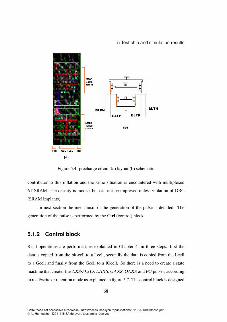
5 Test chip and simulation results
Figure 5.4: precharge circuit (a) layout (b) schematic
contributor to this inflation and the same situation is encountered with multiplexed
6T SRAM. The density is modest but can not be improved unless violation of DRC
(SRAM implants).
In next section the mechanism of the generation of the pulse is detailed. The
generation of the pulse is performed by the Ctrl (control) block.
5.1.2 Control block
Read operations are performed, as explained in Chapter 4, in three steps: first the
data is copied from the bit-cell to a Lcell, secondly the data is copied from the Lcell
to a Gcell and finally from the Gcell to a IOcell. So there is a need to create a state
machine that creates the AXS<0:31>, LAXS, GAXS, OAXS and PG pulses, according
to read/write or retention mode as explained in figure 5.7. The control block is designed
68
Cette thèse est accessible à l'adresse : http://theses.insa-lyon.fr/publication/2011ISAL0013/these.pdf © [L. Hamouche], [2011], INSA de Lyon, tous droits réservés
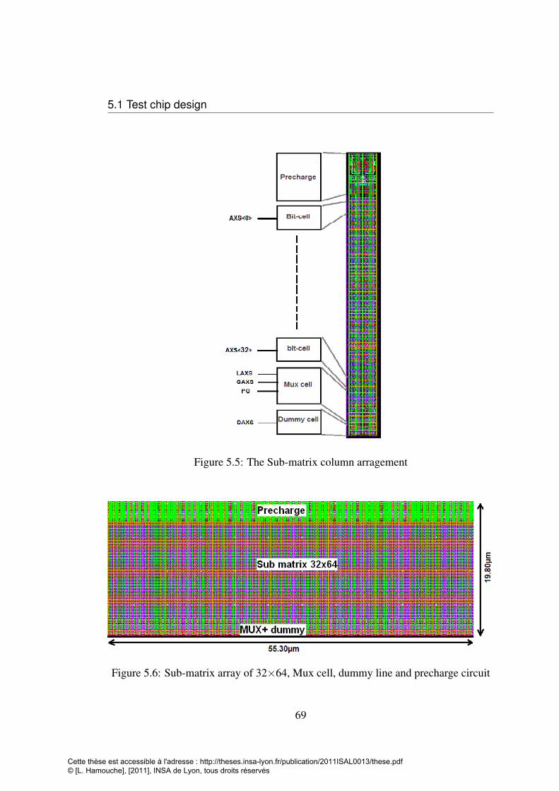
5.1 Test chip design
Figure 5.5: The Sub-matrix column arragement
Figure 5.6: Sub-matrix array of 32×64, Mux cell, dummy line and precharge circuit
69
Cette thèse est accessible à l'adresse : http://theses.insa-lyon.fr/publication/2011ISAL0013/these.pdf © [L. Hamouche], [2011], INSA de Lyon, tous droits réservés
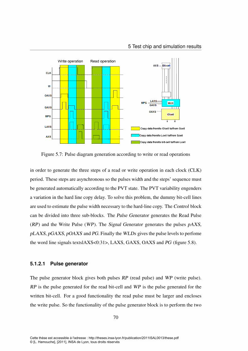
5 Test chip and simulation results
Figure 5.7: Pulse diagram generation according to write or read operations
in order to generate the three steps of a read or write operation in each clock (CLK)
period. These steps are asynchronous so the pulses width and the steps’ sequence must
be generated automatically according to the PVT state. The PVT variability engenders
a variation in the hard line copy delay. To solve this problem, the dummy bit-cell lines
are used to estimate the pulse width necessary to the hard-line copy. The Control block
can be divided into three sub-blocks. The Pulse Generator generates the Read Pulse
(RP ) and the Write Pulse (WP ). The Signal Generator generates the pulses pAXS,
pLAXS, pGAXS, pOAXS and PG. Finally the WLDs gives the pulse levels to perfome
the word line signals textslAXS<0:31>, LAXS, GAXS, OAXS and PG (figure 5.8).
5.1.2.1 Pulse generator
The pulse generator block gives both pulses RP (read pulse) and WP (write pulse).
RP is the pulse generated for the read bit-cell and WP is the pulse generated for the
written bit-cell. For a good functionality the read pulse must be larger and encloses
the write pulse. So the functionality of the pulse generator block is to perform the two
70
Cette thèse est accessible à l'adresse : http://theses.insa-lyon.fr/publication/2011ISAL0013/these.pdf © [L. Hamouche], [2011], INSA de Lyon, tous droits réservés
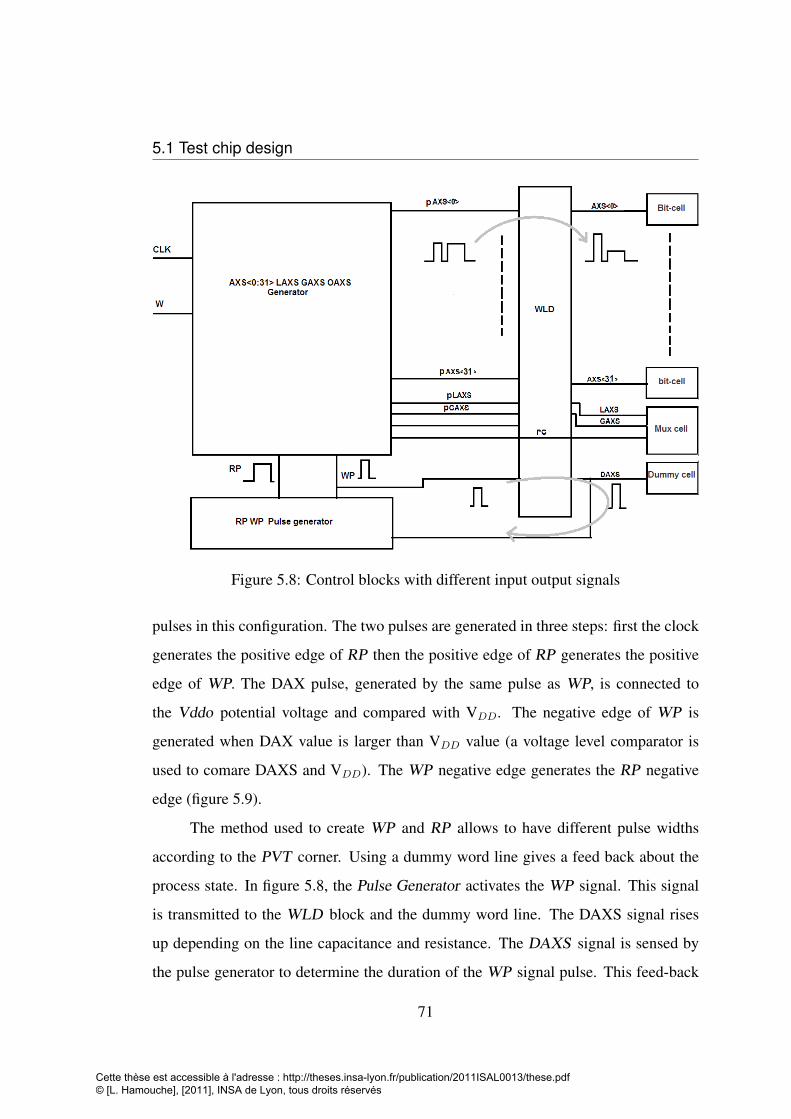
5.1 Test chip design
Figure 5.8: Control blocks with different input output signals
pulses in this configuration. The two pulses are generated in three steps: first the clock
generates the positive edge of RP then the positive edge of RP generates the positive
edge of WP. The DAX pulse, generated by the same pulse as WP, is connected to
the Vddo potential voltage and compared with VDD. The negative edge of WP is
generated when DAX value is larger than VDD value (a voltage level comparator is
used to comare DAXS and VDD). The WP negative edge generates the RP negative
edge (figure 5.9).
The method used to create WP and RP allows to have different pulse widths
according to the PVT corner. Using a dummy word line gives a feed back about the
process state. In figure 5.8, the Pulse Generator activates the WP signal. This signal
is transmitted to the WLD block and the dummy word line. The DAXS signal rises
up depending on the line capacitance and resistance. The DAXS signal is sensed by
the pulse generator to determine the duration of the WP signal pulse. This feed-back
71
Cette thèse est accessible à l'adresse : http://theses.insa-lyon.fr/publication/2011ISAL0013/these.pdf © [L. Hamouche], [2011], INSA de Lyon, tous droits réservés
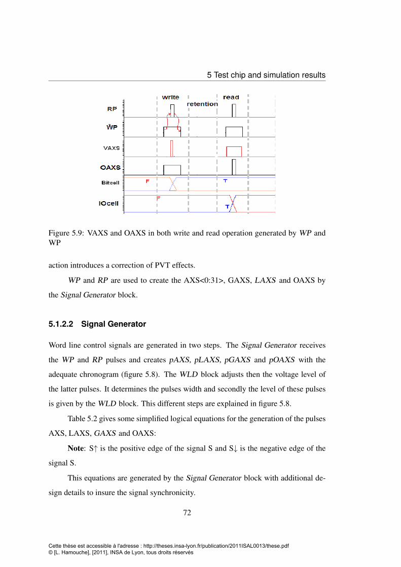
5 Test chip and simulation results
Figure 5.9: VAXS and OAXS in both write and read operation generated by WP andWP
action introduces a correction of PVT effects.
WP and RP are used to create the AXS<0:31>, GAXS, LAXS and OAXS by
the Signal Generator block.
5.1.2.2 Signal Generator
Word line control signals are generated in two steps. The Signal Generator receives
the WP and RP pulses and creates pAXS, pLAXS, pGAXS and pOAXS with the
adequate chronogram (figure 5.8). The WLD block adjusts then the voltage level of
the latter pulses. It determines the pulses width and secondly the level of these pulses
is given by the WLD block. This different steps are explained in figure 5.8.
Table 5.2 gives some simplified logical equations for the generation of the pulses
AXS, LAXS, GAXS and OAXS:
Note: S↑ is the positive edge of the signal S and S↓ is the negative edge of the
signal S.
This equations are generated by the Signal Generator block with additional de-
sign details to insure the signal synchronicity.
72
Cette thèse est accessible à l'adresse : http://theses.insa-lyon.fr/publication/2011ISAL0013/these.pdf © [L. Hamouche], [2011], INSA de Lyon, tous droits réservés
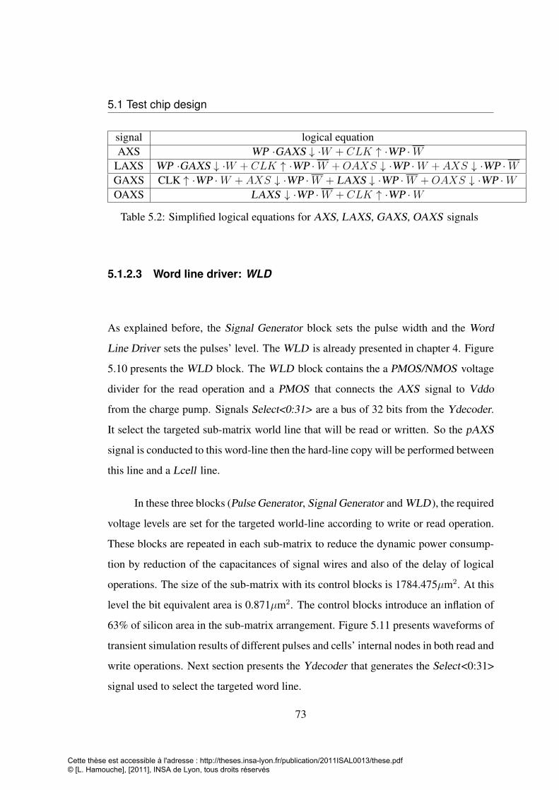
5.1 Test chip design
signal logical equationAXS WP ·GAXS ↓ ·W + CLK ↑ ·WP ·W
LAXS WP ·GAXS ↓ ·W + CLK ↑ ·WP ·W +OAXS ↓ ·WP ·W + AXS ↓ ·WP ·WGAXS CLK ↑ ·WP ·W + AXS ↓ ·WP ·W + LAXS ↓ ·WP ·W +OAXS ↓ ·WP ·WOAXS LAXS ↓ ·WP ·W + CLK ↑ ·WP ·W
Table 5.2: Simplified logical equations for AXS, LAXS, GAXS, OAXS signals
5.1.2.3 Word line driver: WLD
As explained before, the Signal Generator block sets the pulse width and the Word
Line Driver sets the pulses’ level. The WLD is already presented in chapter 4. Figure
5.10 presents the WLD block. The WLD block contains the a PMOS/NMOS voltage
divider for the read operation and a PMOS that connects the AXS signal to Vddo
from the charge pump. Signals Select<0:31> are a bus of 32 bits from the Ydecoder.
It select the targeted sub-matrix world line that will be read or written. So the pAXS
signal is conducted to this word-line then the hard-line copy will be performed between
this line and a Lcell line.
In these three blocks (Pulse Generator, Signal Generator and WLD ), the required
voltage levels are set for the targeted world-line according to write or read operation.
These blocks are repeated in each sub-matrix to reduce the dynamic power consump-
tion by reduction of the capacitances of signal wires and also of the delay of logical
operations. The size of the sub-matrix with its control blocks is 1784.475µm2. At this
level the bit equivalent area is 0.871µm2. The control blocks introduce an inflation of
63% of silicon area in the sub-matrix arrangement. Figure 5.11 presents waveforms of
transient simulation results of different pulses and cells’ internal nodes in both read and
write operations. Next section presents the Ydecoder that generates the Select<0:31>
signal used to select the targeted word line.
73
Cette thèse est accessible à l'adresse : http://theses.insa-lyon.fr/publication/2011ISAL0013/these.pdf © [L. Hamouche], [2011], INSA de Lyon, tous droits réservés
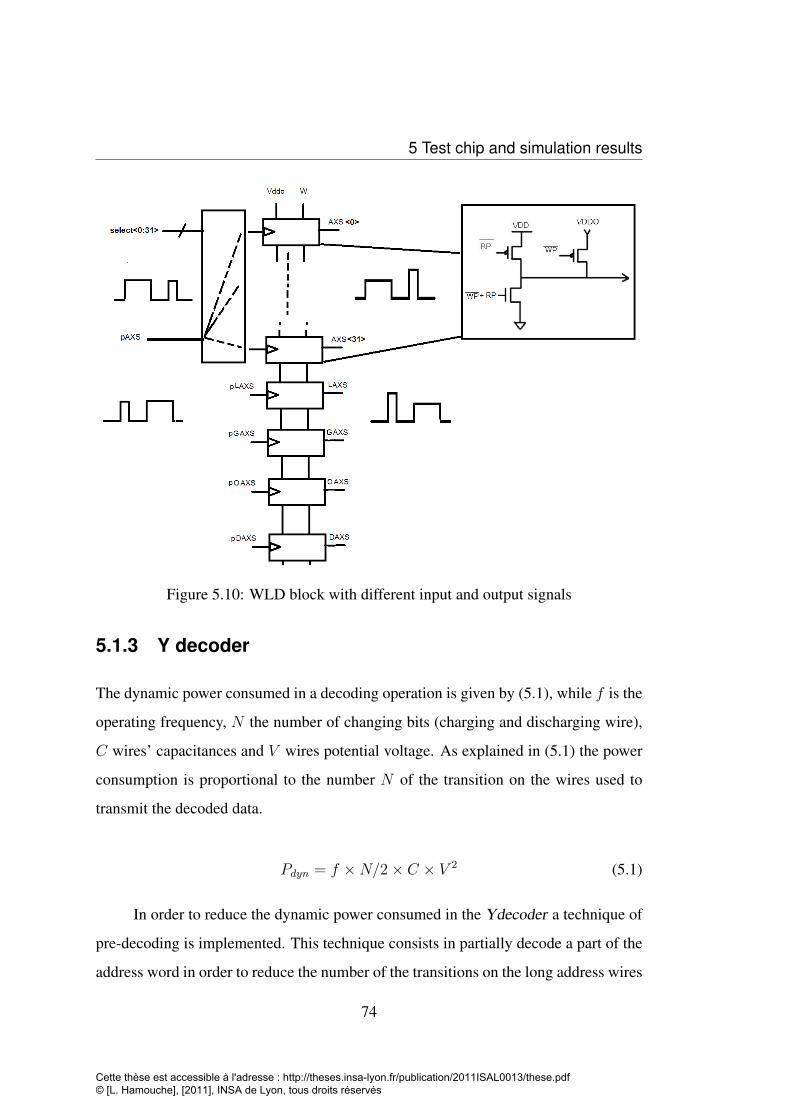
5 Test chip and simulation results
Figure 5.10: WLD block with different input and output signals
5.1.3 Y decoder
The dynamic power consumed in a decoding operation is given by (5.1), while f is the
operating frequency, N the number of changing bits (charging and discharging wire),
C wires’ capacitances and V wires potential voltage. As explained in (5.1) the power
consumption is proportional to the number N of the transition on the wires used to
transmit the decoded data.
Pdyn = f ×N/2× C × V 2 (5.1)
In order to reduce the dynamic power consumed in the Ydecoder a technique of
pre-decoding is implemented. This technique consists in partially decode a part of the
address word in order to reduce the number of the transitions on the long address wires
74
Cette thèse est accessible à l'adresse : http://theses.insa-lyon.fr/publication/2011ISAL0013/these.pdf © [L. Hamouche], [2011], INSA de Lyon, tous droits réservés
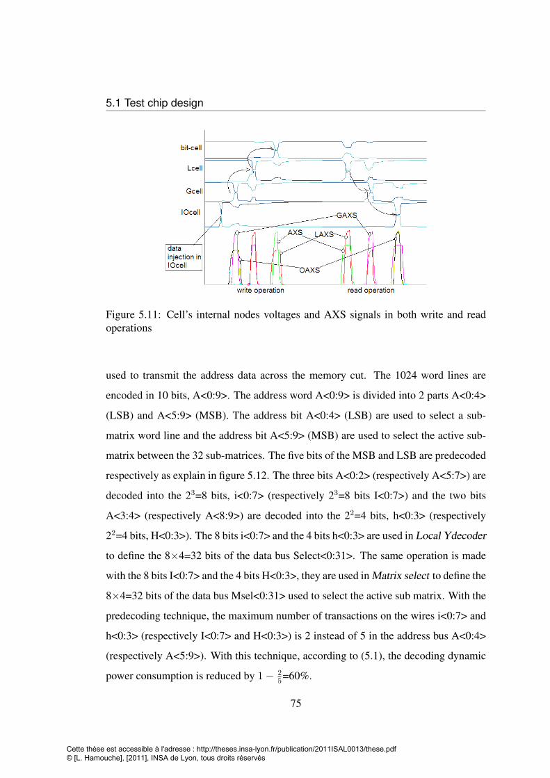
5.1 Test chip design
Figure 5.11: Cell’s internal nodes voltages and AXS signals in both write and readoperations
used to transmit the address data across the memory cut. The 1024 word lines are
encoded in 10 bits, A<0:9>. The address word A<0:9> is divided into 2 parts A<0:4>
(LSB) and A<5:9> (MSB). The address bit A<0:4> (LSB) are used to select a sub-
matrix word line and the address bit A<5:9> (MSB) are used to select the active sub-
matrix between the 32 sub-matrices. The five bits of the MSB and LSB are predecoded
respectively as explain in figure 5.12. The three bits A<0:2> (respectively A<5:7>) are
decoded into the 23=8 bits, i<0:7> (respectively 23=8 bits I<0:7>) and the two bits
A<3:4> (respectively A<8:9>) are decoded into the 22=4 bits, h<0:3> (respectively
22=4 bits, H<0:3>). The 8 bits i<0:7> and the 4 bits h<0:3> are used in Local Ydecoder
to define the 8×4=32 bits of the data bus Select<0:31>. The same operation is made
with the 8 bits I<0:7> and the 4 bits H<0:3>, they are used in Matrix select to define the
8×4=32 bits of the data bus Msel<0:31> used to select the active sub matrix. With the
predecoding technique, the maximum number of transactions on the wires i<0:7> and
h<0:3> (respectively I<0:7> and H<0:3>) is 2 instead of 5 in the address bus A<0:4>
(respectively A<5:9>). With this technique, according to (5.1), the decoding dynamic
power consumption is reduced by 1− 25=60%.
75
Cette thèse est accessible à l'adresse : http://theses.insa-lyon.fr/publication/2011ISAL0013/these.pdf © [L. Hamouche], [2011], INSA de Lyon, tous droits réservés
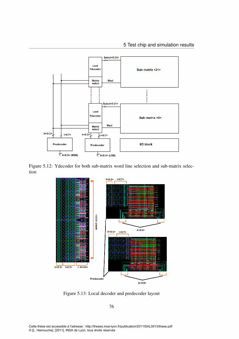
5 Test chip and simulation results
Figure 5.12: Ydecoder for both sub-matrix word line selection and sub-matrix selec-tion
Figure 5.13: Local decoder and predecoder layout
76
Cette thèse est accessible à l'adresse : http://theses.insa-lyon.fr/publication/2011ISAL0013/these.pdf © [L. Hamouche], [2011], INSA de Lyon, tous droits réservés
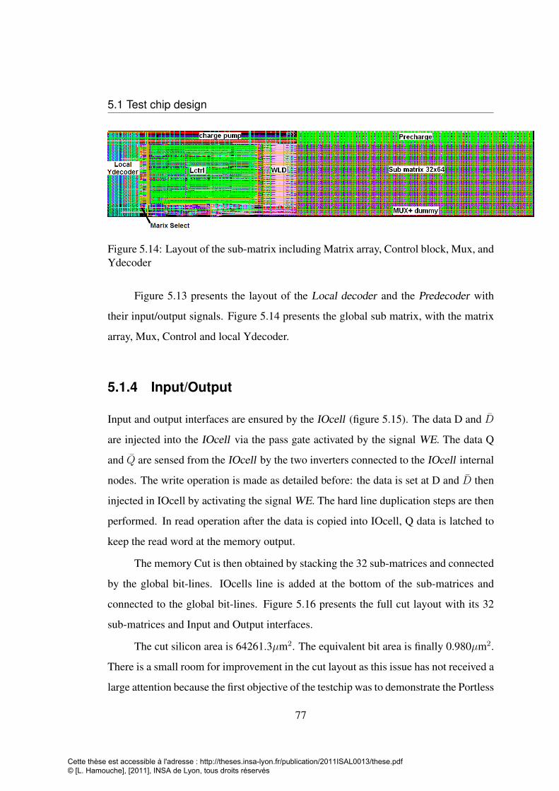
5.1 Test chip design
Figure 5.14: Layout of the sub-matrix including Matrix array, Control block, Mux, andYdecoder
Figure 5.13 presents the layout of the Local decoder and the Predecoder with
their input/output signals. Figure 5.14 presents the global sub matrix, with the matrix
array, Mux, Control and local Ydecoder.
5.1.4 Input/Output
Input and output interfaces are ensured by the IOcell (figure 5.15). The data D and D
are injected into the IOcell via the pass gate activated by the signal WE. The data Q
and Q are sensed from the IOcell by the two inverters connected to the IOcell internal
nodes. The write operation is made as detailed before: the data is set at D and D then
injected in IOcell by activating the signal WE. The hard line duplication steps are then
performed. In read operation after the data is copied into IOcell, Q data is latched to
keep the read word at the memory output.
The memory Cut is then obtained by stacking the 32 sub-matrices and connected
by the global bit-lines. IOcells line is added at the bottom of the sub-matrices and
connected to the global bit-lines. Figure 5.16 presents the full cut layout with its 32
sub-matrices and Input and Output interfaces.
The cut silicon area is 64261.3µm2. The equivalent bit area is finally 0.980µm2.
There is a small room for improvement in the cut layout as this issue has not received a
large attention because the first objective of the testchip was to demonstrate the Portless
77
Cette thèse est accessible à l'adresse : http://theses.insa-lyon.fr/publication/2011ISAL0013/these.pdf © [L. Hamouche], [2011], INSA de Lyon, tous droits réservés
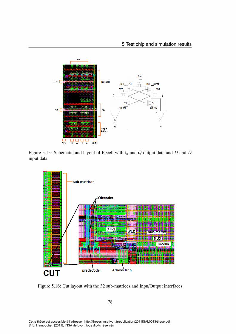
5 Test chip and simulation results
Figure 5.15: Schematic and layout of IOcell with Q and Q output data and D and Dinput data
Figure 5.16: Cut layout with the 32 sub-matrices and Inpu/Output interfaces
78
Cette thèse est accessible à l'adresse : http://theses.insa-lyon.fr/publication/2011ISAL0013/these.pdf © [L. Hamouche], [2011], INSA de Lyon, tous droits réservés

5.2 Simulation results
Figure 5.17: Bit effective area
operability in 32nm. Figure 5.17 pictures the contributors to the effective bit silicon
area. The bit-cell weights 40% of the bit effective area. The hard line duplication
technique and multiplexers occupy 49% including the control blocks. It is the price to
pay for the bit-cell performances. The control blocks (34% of the area) have not been
optimized in layout and extra spaces have been managed in advance of an eventual
correction of the testchip.
5.2 Simulation results
The full cut contains more than 4·105 transistors. Simulating the full cut with "Eldo"
takes several hours for just one cycle of write/retention/read operations. Two ap-
proaches are developed to overcome this simulation issue. First it is possible to lighten
the netlist by creating a Critical Path that represents just the set of necessary bit-cells or
columns where the targeted parameters (delay, consumption, functionality ...) should
appear in a worst case. The rest of the cut is replaced by its equivalent load (figure
5.18). The load is modeled as an RC delay. Resistance and capacitance values are
estimated from the extracted netlist (full LVS). A second approach is to simulate the
79
Cette thèse est accessible à l'adresse : http://theses.insa-lyon.fr/publication/2011ISAL0013/these.pdf © [L. Hamouche], [2011], INSA de Lyon, tous droits réservés
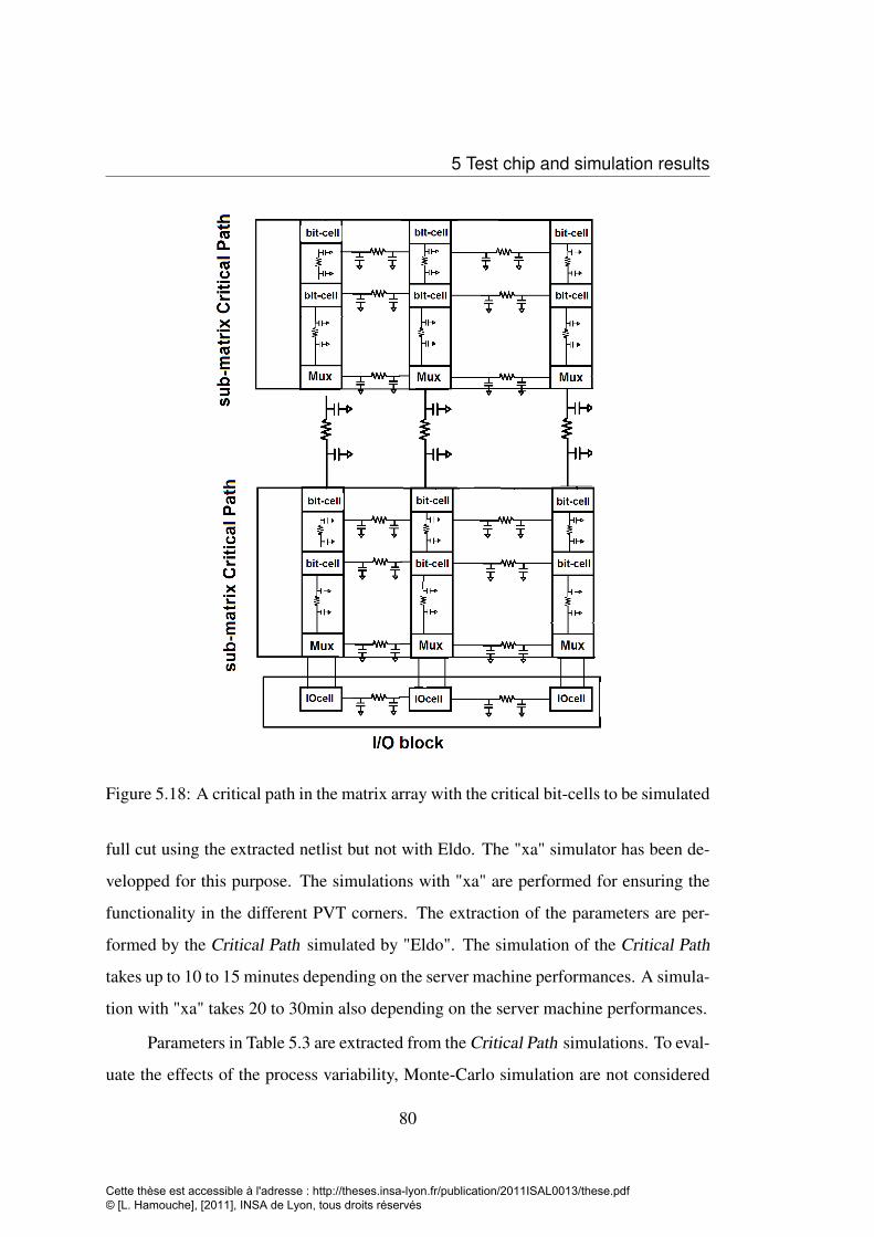
5 Test chip and simulation results
Figure 5.18: A critical path in the matrix array with the critical bit-cells to be simulated
full cut using the extracted netlist but not with Eldo. The "xa" simulator has been de-
velopped for this purpose. The simulations with "xa" are performed for ensuring the
functionality in the different PVT corners. The extraction of the parameters are per-
formed by the Critical Path simulated by "Eldo". The simulation of the Critical Path
takes up to 10 to 15 minutes depending on the server machine performances. A simula-
tion with "xa" takes 20 to 30min also depending on the server machine performances.
Parameters in Table 5.3 are extracted from the Critical Path simulations. To eval-
uate the effects of the process variability, Monte-Carlo simulation are not considered
80
Cette thèse est accessible à l'adresse : http://theses.insa-lyon.fr/publication/2011ISAL0013/these.pdf © [L. Hamouche], [2011], INSA de Lyon, tous droits réservés
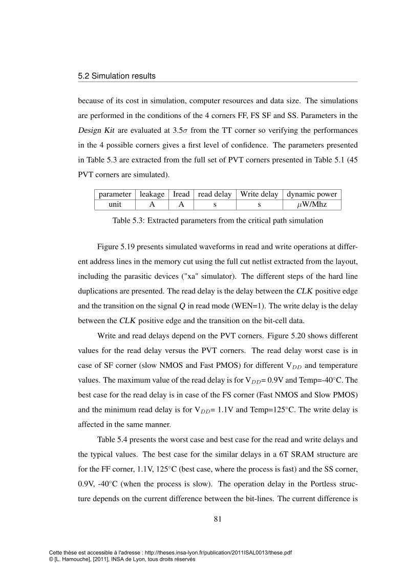
5.2 Simulation results
because of its cost in simulation, computer resources and data size. The simulations
are performed in the conditions of the 4 corners FF, FS SF and SS. Parameters in the
Design Kit are evaluated at 3.5σ from the TT corner so verifying the performances
in the 4 possible corners gives a first level of confidence. The parameters presented
in Table 5.3 are extracted from the full set of PVT corners presented in Table 5.1 (45
PVT corners are simulated).
parameter leakage Iread read delay Write delay dynamic powerunit A A s s µW/Mhz
Table 5.3: Extracted parameters from the critical path simulation
Figure 5.19 presents simulated waveforms in read and write operations at differ-
ent address lines in the memory cut using the full cut netlist extracted from the layout,
including the parasitic devices ("xa" simulator). The different steps of the hard line
duplications are presented. The read delay is the delay between the CLK positive edge
and the transition on the signal Q in read mode (WEN=1). The write delay is the delay
between the CLK positive edge and the transition on the bit-cell data.
Write and read delays depend on the PVT corners. Figure 5.20 shows different
values for the read delay versus the PVT corners. The read delay worst case is in
case of SF corner (slow NMOS and Fast PMOS) for different VDD and temperature
values. The maximum value of the read delay is for VDD= 0.9V and Temp=-40◦C. The
best case for the read delay is in case of the FS corner (Fast NMOS and Slow PMOS)
and the minimum read delay is for VDD= 1.1V and Temp=125◦C. The write delay is
affected in the same manner.
Table 5.4 presents the worst case and best case for the read and write delays and
the typical values. The best case for the similar delays in a 6T SRAM structure are
for the FF corner, 1.1V, 125◦C (best case, where the process is fast) and the SS corner,
0.9V, -40◦C (when the process is slow). The operation delay in the Portless struc-
ture depends on the current difference between the bit-lines. The current difference is
81
Cette thèse est accessible à l'adresse : http://theses.insa-lyon.fr/publication/2011ISAL0013/these.pdf © [L. Hamouche], [2011], INSA de Lyon, tous droits réservés
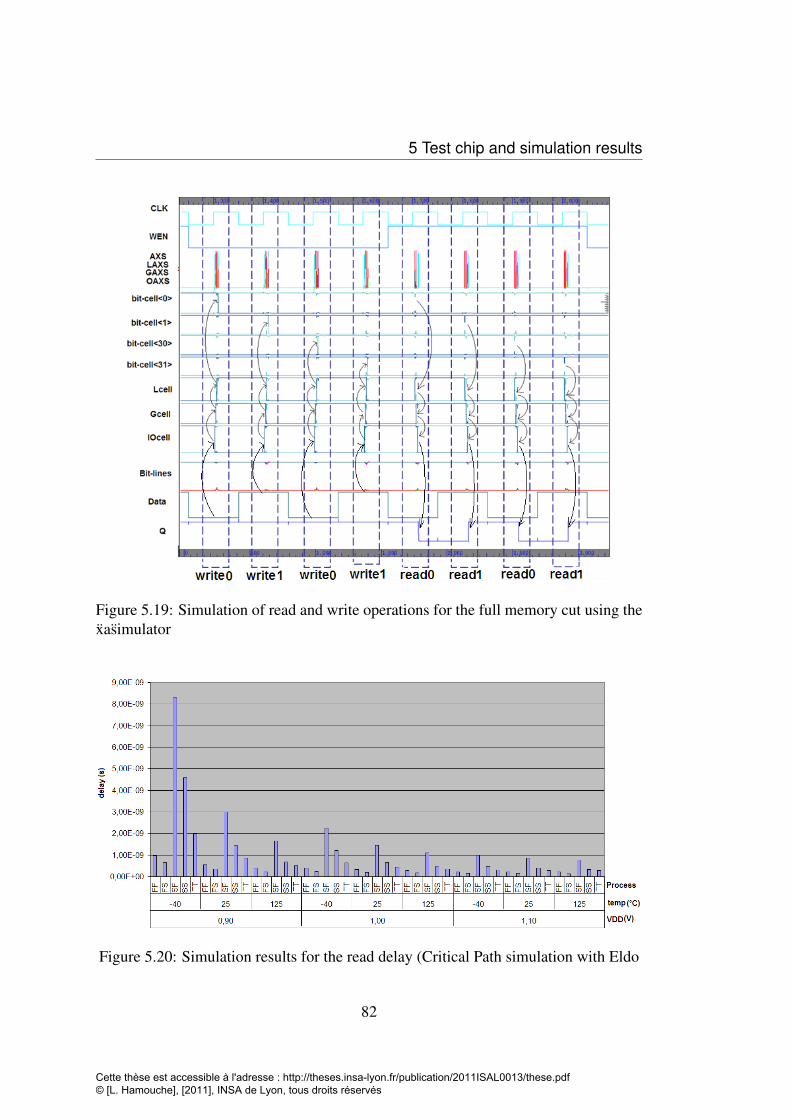
5 Test chip and simulation results
Figure 5.19: Simulation of read and write operations for the full memory cut using thexasimulator
Figure 5.20: Simulation results for the read delay (Critical Path simulation with Eldo
82
Cette thèse est accessible à l'adresse : http://theses.insa-lyon.fr/publication/2011ISAL0013/these.pdf © [L. Hamouche], [2011], INSA de Lyon, tous droits réservés
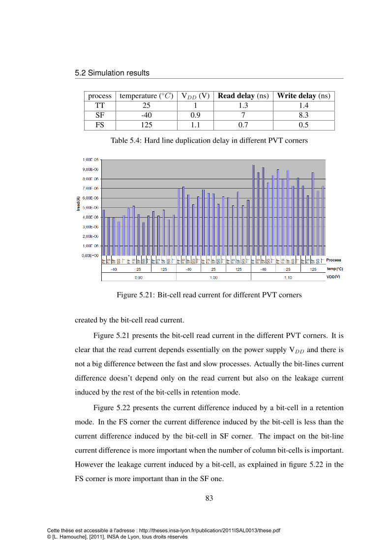
5.2 Simulation results
process temperature (◦C) VDD (V) Read delay (ns) Write delay (ns)TT 25 1 1.3 1.4SF -40 0.9 7 8.3FS 125 1.1 0.7 0.5
Table 5.4: Hard line duplication delay in different PVT corners
Figure 5.21: Bit-cell read current for different PVT corners
created by the bit-cell read current.
Figure 5.21 presents the bit-cell read current in the different PVT corners. It is
clear that the read current depends essentially on the power supply VDD and there is
not a big difference between the fast and slow processes. Actually the bit-lines current
difference doesn’t depend only on the read current but also on the leakage current
induced by the rest of the bit-cells in retention mode.
Figure 5.22 presents the current difference induced by a bit-cell in a retention
mode. In the FS corner the current difference induced by the bit-cell is less than the
current difference induced by the bit-cell in SF corner. The impact on the bit-line
current difference is more important when the number of column bit-cells is important.
However the leakage current induced by a bit-cell, as explained in figure 5.22 in the
FS corner is more important than in the SF one.
83
Cette thèse est accessible à l'adresse : http://theses.insa-lyon.fr/publication/2011ISAL0013/these.pdf © [L. Hamouche], [2011], INSA de Lyon, tous droits réservés
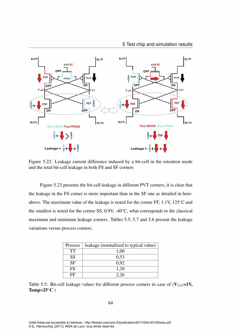
5 Test chip and simulation results
Figure 5.22: Leakage current difference induced by a bit-cell in the retention modeand the total bit-cell leakage in both FS and SF corners
Figure 5.23 presents the bit-cell leakage in different PVT corners, it is clear that
the leakage in the FS corner is more important than in the SF one as detailed in here-
above. The maximum value of the leakage is noted for the corner FF, 1.1V, 125◦C and
the smallest is noted for the corner SS, 0.9V, -40◦C, what corresponds to the classical
maximum and minimum leakage corners. Tables 5.5, 5.7 and 5.6 present the leakage
variations versus process corners.
Process leakage (normalized to typical value)TT 1,00SS 0,53SF 0,92FS 1,39FF 2,26
Table 5.5: Bit-cell leakage values for different process corners in case of (VDD=1V,Temp=25◦C )
84
Cette thèse est accessible à l'adresse : http://theses.insa-lyon.fr/publication/2011ISAL0013/these.pdf © [L. Hamouche], [2011], INSA de Lyon, tous droits réservés
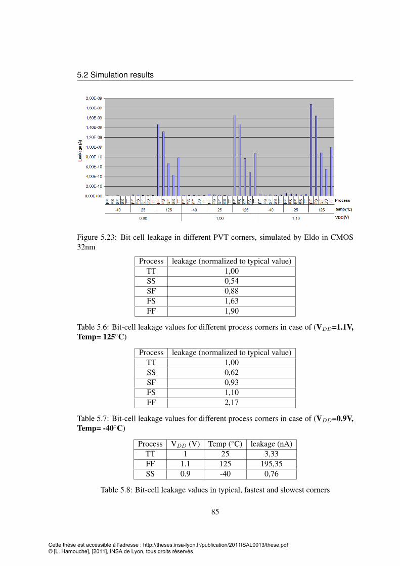
5.2 Simulation results
Figure 5.23: Bit-cell leakage in different PVT corners, simulated by Eldo in CMOS32nm
Process leakage (normalized to typical value)TT 1,00SS 0,54SF 0,88FS 1,63FF 1,90
Table 5.6: Bit-cell leakage values for different process corners in case of (VDD=1.1V,Temp= 125◦C)
Process leakage (normalized to typical value)TT 1,00SS 0,62SF 0,93FS 1,10FF 2,17
Table 5.7: Bit-cell leakage values for different process corners in case of (VDD=0.9V,Temp= -40◦C)
Process VDD (V) Temp (◦C) leakage (nA)TT 1 25 3,33FF 1.1 125 195,35SS 0.9 -40 0,76
Table 5.8: Bit-cell leakage values in typical, fastest and slowest corners
85
Cette thèse est accessible à l'adresse : http://theses.insa-lyon.fr/publication/2011ISAL0013/these.pdf © [L. Hamouche], [2011], INSA de Lyon, tous droits réservés
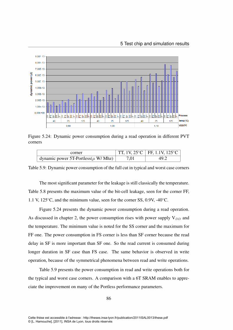
5 Test chip and simulation results
Figure 5.24: Dynamic power consumption during a read operation in different PVTcorners
corner TT, 1V, 25◦C FF, 1.1V, 125◦Cdynamic power 5T-Portless(µ W/ Mhz) 7,01 49.2
Table 5.9: Dynamic power consumption of the full cut in typical and worst case corners
The most significant parameter for the leakage is still classically the temperature.
Table 5.8 presents the maximum value of the bit-cell leakage, seen for the corner FF,
1.1 V, 125◦C, and the minimum value, seen for the corner SS, 0.9V, -40◦C.
Figure 5.24 presents the dynamic power consumption during a read operation.
As discussed in chapter 2, the power consumption rises with power supply VDD and
the temperature. The minimum value is noted for the SS corner and the maximum for
FF one. The power consumption in FS corner is less than SF corner because the read
delay in SF is more important than SF one. So the read current is consumed during
longer duration in SF case than FS case. The same behavior is observed in write
operation, because of the symmetrical phenomena between read and write operations.
Table 5.9 presents the power consumption in read and write operations both for
the typical and worst case corners. A comparison with a 6T SRAM enables to appre-
ciate the improvement on many of the Portless performance parameters.
86
Cette thèse est accessible à l'adresse : http://theses.insa-lyon.fr/publication/2011ISAL0013/these.pdf © [L. Hamouche], [2011], INSA de Lyon, tous droits réservés
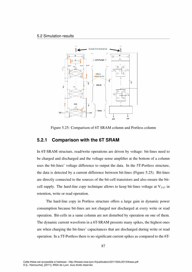
5.2 Simulation results
Figure 5.25: Comparison of 6T SRAM column and Portless column
5.2.1 Comparison with the 6T SRAM
In 6T-SRAM structure, read/write operations are driven by voltage: bit-lines need to
be charged and discharged and the voltage sense amplifier at the bottom of a column
uses the bit-lines’ voltage difference to output the data. In the 5T-Portless structure,
the data is detected by a current difference between bit-lines (Figure 5.25). Bit-lines
are directly connected to the sources of the bit-cell transistors and also ensure the bit-
cell supply. The hard-line copy technique allows to keep bit-lines voltage at VDD in
retention, write or read operation.
The hard-line copy in Portless structure offers a large gain in dynamic power
consumption because bit-lines are not charged nor discharged at every write or read
operation. Bit-cells in a same column are not disturbed by operation on one of them.
The dynamic current waveform in a 6T-SRAM presents many spikes, the highest ones
are when charging the bit-lines’ capacitances that are discharged during write or read
operation. In a 5T-Portless there is no significant current spikes as compared to the 6T-
87
Cette thèse est accessible à l'adresse : http://theses.insa-lyon.fr/publication/2011ISAL0013/these.pdf © [L. Hamouche], [2011], INSA de Lyon, tous droits réservés
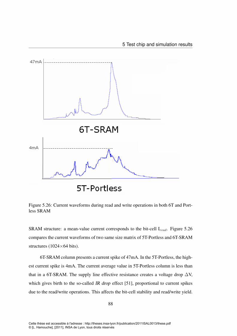
5 Test chip and simulation results
Figure 5.26: Current waveforms during read and write operations in both 6T and Port-less SRAM
SRAM structure: a mean-value current corresponds to the bit-cell Iread. Figure 5.26
compares the current waveforms of two same size matrix of 5T-Portless and 6T-SRAM
structures (1024×64 bits).
6T-SRAM column presents a current spike of 47mA. In the 5T-Portless, the high-
est current spike is 4mA. The current average value in 5T-Portless column is less than
that in a 6T-SRAM. The supply line effective resistance creates a voltage drop ∆V,
which gives birth to the so-called IR drop effect [51], proportional to current spikes
due to the read/write operations. This affects the bit-cell stability and read/write yield.
88
Cette thèse est accessible à l'adresse : http://theses.insa-lyon.fr/publication/2011ISAL0013/these.pdf © [L. Hamouche], [2011], INSA de Lyon, tous droits réservés
5.3 Testchip Results
corner TT, 1V, 25◦C FF, 1.1V, 125◦Cleakage Portless RVT cell 3,32609E-11 6,30244E-09
leakage 6T(H187) cell 5,5E-11 9,65E-09leakage Portless vs 6T -39,53% -34,69%
Table 5.10: Leakage current values comparison between Portless and 6T SRAM bit-cells
corner TT, 1V, 25◦C FF, 1.1V, 125◦Cpower dynamic 5T-Portless (µW/Mhz) 7.01 12.316T SRAM cut (1024x64) (µW/Mhz) 10.65 14.84
power dynamic 5T vs 6T -0.34% -0.17%
Table 5.11: Leakage current values comparison between Portless and 6T SRAM bit-cells
Current mode read/write in Portless is immune from VDD fluctuations due to current
spike.
Table 5.10 presents a comparison of leakage current in Portless bit-cell and 6T
SRAM (typical corner). A gain of 39% in static consumption is observed in the case
of the typical Corner in favor of the Portless.
Table 5.11 presents dynamic power comparison between Portless and 6T SRAM.
A gain of 34% is noted in typical corner and 17% in worst case.
Next section gives a summary of the available measurements on the 32nm testchip
submitted for fabrication by Samsung.
5.3 Testchip Results
The test chip has been designed with RVT transistors as offered by the design kit
(Regular Vth). Standard DRC rules have been applied. The periphery is not voluntarily
optimized to guarantee the functionality in CMOS 32nm (space reserves have been
managed in anticipation of correction of the first testchip). It was known at the time
of submission to fabrication that the results obtained for delays, Leakage and dynamic
89
Cette thèse est accessible à l'adresse : http://theses.insa-lyon.fr/publication/2011ISAL0013/these.pdf © [L. Hamouche], [2011], INSA de Lyon, tous droits réservés
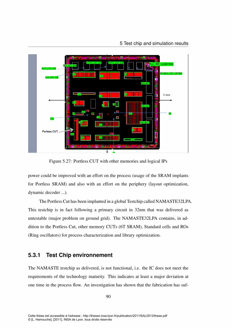
5 Test chip and simulation results
Figure 5.27: Portless CUT with other memories and logical IPs
power could be improved with an effort on the process (usage of the SRAM implants
for Portless SRAM) and also with an effort on the periphery (layout optimization,
dynamic decoder ...).
The Portless Cut has been implanted in a global Testchip called NAMASTE32LPA.
This testchip is in fact following a primary circuit in 32nm that was delivered as
untestable (major problem on ground grid). The NAMASTE32LPA contains, in ad-
dition to the Portless Cut, other memory CUTs (6T SRAM), Standard cells and ROs
(Ring oscillators) for process characterization and library optimization.
5.3.1 Test Chip environnement
The NAMASTE testchip as delivered, is not functional, i.e. the IC does not meet the
requirements of the technology maturity. This indicates at least a major deviation at
one time in the process flow. An investigation has shown that the fabrication has suf-
90
Cette thèse est accessible à l'adresse : http://theses.insa-lyon.fr/publication/2011ISAL0013/these.pdf © [L. Hamouche], [2011], INSA de Lyon, tous droits réservés
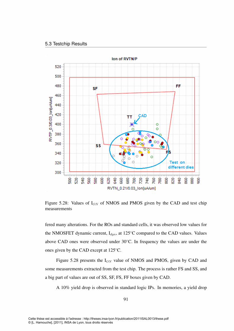
5.3 Testchip Results
Figure 5.28: Values of ION of NMOS and PMOS given by the CAD and test chipmeasurements
fered many alterations. For the ROs and standard cells, it was observed low values for
the NMOSFET dynamic current, Idyn, at 125◦C compared to the CAD values. Values
above CAD ones were observed under 30◦C. In frequency the values are under the
ones given by the CAD except at 125◦C.
Figure 5.28 presents the ION value of NMOS and PMOS, given by CAD and
some measurements extracted from the test chip. The process is rather FS and SS, and
a big part of values are out of SS, SF, FS, FF boxes given by CAD.
A 10% yield drop is observed in standard logic IPs. In memories, a yield drop
91
Cette thèse est accessible à l'adresse : http://theses.insa-lyon.fr/publication/2011ISAL0013/these.pdf © [L. Hamouche], [2011], INSA de Lyon, tous droits réservés
5 Test chip and simulation results
is also evaluated at least of 10% and near to 17%. The maximum frequency of ring
oscillators observed in the test chip is under the pessimistic values given by the CAD.
The leakage measured for different blocks in the test chip are largely above the CAD
ones.
The test chip report concludes that wide devices are out of specifications. Other
devices are close to the specifications but not on target. Wide devices behavior makes
the silicon vs CAD comparison difficult for memories (given the variety of transistors
width in memory peripheries). It is impossible to conclude on the Portless functional-
ity. CMOS 32nm industrial maturity cannot be performed on this lot. A new silicon
is needed to prove first the industrial maturity of the CMOS 32nm. Then it will be
possible to verify the performances of the NAMASTE testchip.
5.3.2 Portlesss Results
The large variation on the measurement dynamic current and leakage current is indica-
tive of a high drop in fabrication yield. The large difference between CAD and silicon
results, makes it difficult to characterize the memory cut. As is the case for the other
devices, the leakage measurement on the Portless Cut is largely above results obtained
on CAD (Figure 5.29). The dynamic power is in specification for temp=125◦C but
above CAD for temp=-40◦C (Figure 5.30).
As concluded in the test chip report, a new silicon is needed to validate the port-
less memory cut. During the period of test chip manufacturing, the Design Kit has
been updated. A new NAMASTE test chip was scheduled using this new Desing Kit.
It includes some DRC modifications, so some modifications are demanded in the lay-
out (essentially on the VIAs). Also some modifications on the design are needed be-
cause characterizations of the transistors have changed. The Portless memory Cut was
redesigned in accordance to the new Design Kit and including the optimization that
were identified at the time of the first design. The Word Line Driver sizing and the
92
Cette thèse est accessible à l'adresse : http://theses.insa-lyon.fr/publication/2011ISAL0013/these.pdf © [L. Hamouche], [2011], INSA de Lyon, tous droits réservés
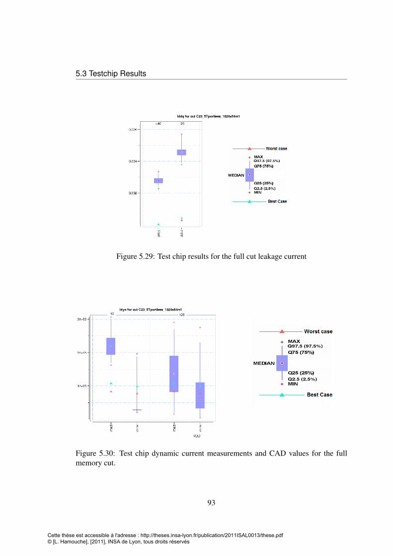
5.3 Testchip Results
Figure 5.29: Test chip results for the full cut leakage current
Figure 5.30: Test chip dynamic current measurements and CAD values for the fullmemory cut.
93
Cette thèse est accessible à l'adresse : http://theses.insa-lyon.fr/publication/2011ISAL0013/these.pdf © [L. Hamouche], [2011], INSA de Lyon, tous droits réservés

5 Test chip and simulation results
Pulse Generator have been modified to reduce the delays in read/write operations and
improve the functionality. The dynamic power consumption is not affected. The po-
tential of some critical nodes have been initialized to guarantee the detection of the
Portless functionality even in the case of a second drop in yield. All simulations for
the verification in different PVT corners have successfully been performed and the test
chip is now in manufacturing line.
94
Cette thèse est accessible à l'adresse : http://theses.insa-lyon.fr/publication/2011ISAL0013/these.pdf © [L. Hamouche], [2011], INSA de Lyon, tous droits réservés
6
Conclusion
SRAM memories and moreover embedded SRAMs face a number of challenges in
coming technology nodes. The magnitude of variations in device performances is
increasing as much as the transistor size decreases according to a σVth = A/√WL
dependence. The exponential increase in memory size with each product generation
amplifies also the impact of the variability. Hence the required manufacturing yield at
the bit-cell level increases proportionally to the memory size, as detailed in Chapter 3.
The leakage current is exponentially increasing at each technology node. The
static power consumption becomes then a significant part in the global chip consump-
tion. Classical techniques for leakage reduction are coming to a limit beyond 45nm.
The reduction in dynamic power consumption is addressed by the power supply (VDD)
scaling. Unfortunately the VDD scaling impacts negatively the SRAM stability. The
trade-off between power consumption and stability becomes difficult to satisfy and
difficult to verify. The Monte-Carlo approach becomes impracticable or insufficient.
Several products now in manufacturing or in development continues to includes
more and more applications but must be low power such as mobile or medical appli-
cations. We live in an always-on world. Some applications must now be always on as
mobile interfaces; some kinds of sensor, supervision systems, medical applications...
These applications can not be in sleep mode. In such applications the power consump-
tion issue is dramatic. The PhD objective was to propose a solution for the SRAM
95
Cette thèse est accessible à l'adresse : http://theses.insa-lyon.fr/publication/2011ISAL0013/these.pdf © [L. Hamouche], [2011], INSA de Lyon, tous droits réservés
6 Conclusion
memory in advanced technology nodes, for embedded always-on applications. Design
solutions were solely investigated. Process options were listed as the state of the art.
In the state of the art, variability impacts were detailed at bit-cell level, bit-cell column
and matrix level. The impact of variability on stability, consumption, density and per-
formances were presented. Some existing solutions have been mentioned with their
limitations in advanced technologies. Some mostly used bit-cells were studied with
their benefits and disadvantages, with respect to variability and power consumption
issues.
The targeted manufacturing yield for the SRAM bit-cell leads to narrower mar-
gin windows notably for the read stability characterized by the Static Noise Margin
(SNM) and the write ability characterized by the Write Margin (WM). Both parame-
ters represent one main design problem now faced by the memory designer. During
the PhD works, a methodology for the variability modeling was studied as summa-
rized in Chapter 3. It is demonstrated that the estimation of an optimal margin with
respect to a given parameter and for a targeted manufacturing yield, can be determined
with a good accuracy. This method costs less effort than the Monte Carlo simulation
and gives more insight. The results of the study were compared to the Monte Carlo
simulations in the case of the 6T bit-cell.
The state of the art concludes that the main contributor in static power consump-
tion (leakage) is the bit-cell. Most of the dynamic consumption is dissipated in the
bit-line capacitances. The 5T Portless bit-cell has been considered for its intrinsic
better dispositions with respect to variability. Moreover the current mode operation
presents an important interest. The absence of Pass Gates transistors reduces the im-
pact of the bit-lines on the bit-cell internal nodes and eliminates their contribution in
term of leakage current. The Portless is then identified as a low leakage and more sta-
ble bit-cell compared to the traditional 6T SRAM. The current mode operation allows
to keep the bit-lines at VDD so the dynamic power consumption is reduced.
96
Cette thèse est accessible à l'adresse : http://theses.insa-lyon.fr/publication/2011ISAL0013/these.pdf © [L. Hamouche], [2011], INSA de Lyon, tous droits réservés
The classical sensing technique does not work in advanced technology nodes
because of increasing offsets. An original technique for write and read operations
was introduced, the hard line duplication. The technique is associated to a particular
operation of the control transistor in the bit-cell (AXS). This contribution defines new
operating conditions for the Portless that extend its functionality beyond the 45nm
node. The hard-line copy allows also the implementation of a low power multiplexed
architecture. In the Portless architecture, the read and write operations are symmetrical
so there is no conflict between them. So this solves the traditional problem in 6T
between the SNM and WM. The IR-drop issue is reduced in Portless structure because
of its low current values and a lack of significant current spikes.
The periphery of the bit-cell matrix arrangement includes the generation of var-
ious control signal. As much as possible, the signals are generated with a correction
against the process status. This participates to the reduction of the impact of variability
and consequently increases the manufacturing yield of the bit-cells.
A layout of 1024x32bits has been developed in standard 32nm CMOS using the
available Design Kit at time of design. The simulation results demonstrate the Portless
benefits in terms of static and dynamic power consumption compared to the 6T SRAM
structure. A read/write operation with an indicative operating frequency of 100 MHz
can be easily achieved. The simulations demonstrate that the 5T Portless is a good
candidate for always-on, limited frequency applications.
The fabricated testchip presents large discrepancies with regards to CAD results.
The large variation of the saturation current, ION , of the transistors and the large value
of the leakage current are caused by a high drop in fabrication yield. A redesign has
been achieved taking advantage of a latest Design Kit that imposed many fixes.
As mentioned in chapter 5, the performances of the Portless structure can be
improved by optimization of the periphery. The bit-cell density can be improved by
necessitates the SRAM implants during the fabrication process. The Portless perfor-
97
Cette thèse est accessible à l'adresse : http://theses.insa-lyon.fr/publication/2011ISAL0013/these.pdf © [L. Hamouche], [2011], INSA de Lyon, tous droits réservés

6 Conclusion
mances would be also improved, simulations show that in the Fast-Slow corner, the
Portless presents less delays and less dynamic power consumption. The SRAM im-
plants bring these benefits.
The main perspective to prove the industrial interest of the Portless is first to
obtain a testchip with a nominal process.
Modeling for variability has been experienced. The modest contribution is suf-
ficient to push for additional efforts. A first step is to develop a similar model for an
other significant parameter and concludes with the benefit of the approach compared
to Monte Carlo simulations. A second step, in fact a dream, would be to get a huge
number of a same test chip, fabricated in different lots and different locations to build a
statistical study of the variability effects. Possessing these experimental results renders
possible to confront the achievement of the proposed modeling approach compared to
a classical procedure. Moreover the experimental results would quantify a real man-
ufacturing yield of the Portless bit-cell. It is a dream because we are talking here of
more than 109 test-chips of 1024 words.
98
Cette thèse est accessible à l'adresse : http://theses.insa-lyon.fr/publication/2011ISAL0013/these.pdf © [L. Hamouche], [2011], INSA de Lyon, tous droits réservés

Cette thèse est accessible à l'adresse : http://theses.insa-lyon.fr/publication/2011ISAL0013/these.pdf © [L. Hamouche], [2011], INSA de Lyon, tous droits réservés

99
Cette thèse est accessible à l'adresse : http://theses.insa-lyon.fr/publication/2011ISAL0013/these.pdf © [L. Hamouche], [2011], INSA de Lyon, tous droits réservés
Bibliography
[1] T. Ohsawa, K. Fujita, K. Hatsuda, T. Higashi, T. Shino, Y. Minami, H. Nakajima,M. Morikado, K. Inoh, T. Hamamoto, S. Watanabe, S. Fujii, and T. Furuyama.Design of a 128-mb SOI DRAM using the floating body cell (FBC). IEEE Jour-nal of Solid-State Circuits, 41(1):135–145, January 2006.
[2] S. Khan and S. Hamdioui. Trends and challenges of sram reliability in the nano-scale era. In Design and Technology of Integrated Systems in Nanoscale Era(DTIS), 2010 5th International Conference on, pages 1 –6, 2010.
[3] Shiao-Li Tsao and E-Cheng Cheng. Energy-conserving always-on schemes for amobile node with multiple interfaces in all-IP network. In Personal, Indoor andMobile Radio Communications, 2007. PIMRC 2007. IEEE 18th InternationalSymposium on, pages 1–5, Athens, 2007.
[4] Wan-Ki Park, Chang sic Choi, Il woo Lee, and Jonghyun Jang. Energy efficientmulti-function home gateway in always-on home environment. IEEE Transac-tions on Consumer Electronics, 56(1):106–111.
[5] D. A. El-Dib, Z. Abid, and H. A. Shawkey. Investigating an aggressive modefor drowsy cache cells. In Canadian Conference on Electrical and ComputerEngineering CCECE., pages 000901–000904, Niagara Falls, ON, 2008.
[6] B. Davydov and V. Gopkalof. Real time energy consumption monitoring as atool for the freight trains dispatching. In 4th IET International Conference onRailway Condition Monitoring, pages 1–2, Derby, 2008.
[7] ITRS. 2008 edition roadmap.
[8] B. Cheng, S. Roy, G. Roy, F. Adamu-Lema, and A. Asenov. Impact of intrinsicparameter fluctuation in decanano MOSFET on a yield and functionality SRAMcell. IEEE Solid-State Electronics, 49, 2005.
[9] F. Boeuf, M. Sellier, A. Farcy, and T. Skotnicki. An evaluation of the CMOStechnology roadmap from the point of view of variability, interconnects, andpower dissipation. IEEE Transactions on Electron Devices, 55(6):1433–1440,June 2008.
100
Cette thèse est accessible à l'adresse : http://theses.insa-lyon.fr/publication/2011ISAL0013/these.pdf © [L. Hamouche], [2011], INSA de Lyon, tous droits réservés
Bibliography
[10] Wei Dong, Peng Li, and G.M. Huang. Sram dynamic stability: Theory, variabilityand analysis. pages 378 –385, 10-13 2008.
[11] T. Skotnicki, G. Merckel, and C. Denat. Mastar - a model for analog simulationof subthreshold, saturation and weak avalanche regions in mosfets. pages 146–147, may. 1993.
[12] M.J.M. Pelgrom, H. Tuinhout, and M. Vertregt. Transistor matching in analogCMOS applications. Proceedings of IEEE International Electron Devices Meet-ing, pages 915–918, 1998.
[13] Zheng Guo, A. Carlson, Liang-Teck Pang, K. T. Duong, Tsu-Jae King Liu, andB. Nikolic. Large-scale SRAM variability characterization in 45 nm CMOS.IEEE Journal of Solid-State Circuits, 44(11):3174–3192, 2009.
[14] S. Chellappa, Jia Ni, Xiaoyin Yao, N. Hindman, J. Velamala, Min Chen, Yu Cao,and L.T. Clark. In-situ characterization and extraction of sram variability. InDesign Automation Conference (DAC), 2010 47th ACM/IEEE, pages 711 –716,2010.
[15] T. Fischer, E. Amirante, P. Huber, T. Nirschl, A. Olbrich, M. Ostermayr, andD. Schmitt-Landsiedel. Analysis of read current and write trip voltage variabilityfrom a 1-MB SRAM test structure. Semiconductor Manufacturing, IEEE Trans-actions on, 21(4):534 –541, 2008.
[16] T. Azam, B. Cheng, and D.R.S. Cumming. Variability resilient low-power 7t-sram design for nano-scaled technologies. In Quality Electronic Design (ISQED),2010 11th International Symposium on, pages 9 –14, 2010.
[17] L. Chang, R. K. Montoye, Y. Nakamura, K. A. Batson, R. J. Eickemeyer, R. H.Dennard, W. Haensch, and D. Jamsek. An 8t-SRAM for variability tolerance andlow-voltage operation in high-performance caches. In Solid-State Circuits, IEEEJournal of, volume 43, pages 956–963, Lille, France, April 2008.
[18] Vita Pi-Ho Hu, Ming-Long Fan, Chien-Yu Hsieh, Pin Su, and Ching-Te Chuang.Finfet sram cell optimization considering temporal variability due to nbti/pbtiand surface orientation. In Simulation of Semiconductor Processes and Devices(SISPAD), 2010 International Conference on, pages 269 –272, 2010.
[19] K. Endo, S. O’uchi, Y. Ishikawa, Y. Liu, T. Matsukawa, K. Sakamoto, J. Tsukada,H. Yamauchi, and M. Masahara. Variability analysis of tin finfet sram cell per-formance and its compensation using vth-controllable independent double-gatefinfet. In VLSI Technology Systems and Applications (VLSI-TSA), 2010 Interna-tional Symposium on, pages 124 –125, 2010.
101
Cette thèse est accessible à l'adresse : http://theses.insa-lyon.fr/publication/2011ISAL0013/these.pdf © [L. Hamouche], [2011], INSA de Lyon, tous droits réservés
Bibliography
[20] Xiao Zhang, Jing Li, M. Grubbs, M. Deal, B. Magyari-Kope, B.M. Clemens, andY. Nishi. Physical model of the impact of metal grain work function variabilityon emerging dual metal gate mosfets and its implication for sram reliability. InElectron Devices Meeting (IEDM), 2009 IEEE International, pages 1 –4, 2009.
[21] S. Mukhopadhyay, Keunwoo Kim, and Ching-Te Chuang. Device design andoptimization methodology for leakage and variability reduction in sub-45-nmFD/SOI SRAM. IEEE Trans. Electron Devices, 55(1):152–162, January 2008.
[22] R. Tsuchiya, N. Sugii, T. Ishigaki, Y. Morita, H. Yoshimoto, K. Torii, andS. Kimura. Low voltage (vdd 0.6 v) sram operation achieved by reduced thresh-old voltage variability in sotb (silicon on thin box). In VLSI Technology, 2009Symposium on, pages 150 –151, 2009.
[23] V.P.-H. Hu, Yu-Sheng Wu, Ming-Long Fan, Pin Su, and Ching-Te Chuang. In-vestigation of static noise margin of ultra-thin-body soi sram cells in subthresholdregion using analytical solution of poisson’s equation. In VLSI Technology, Sys-tems, and Applications, 2009. VLSI-TSA ’09. International Symposium on, pages115 –116, 2009.
[24] M. Suzuki, T. Saraya, K. Shimizu, T. Sakurai, and T. Hiramoto. Post-fabricationself-convergence scheme for suppressing variability in sram cells and logic tran-sistors. In VLSI Technology, 2009 Symposium on, pages 148 –149, 2009.
[25] B. Giraud and A. Amara. Read stability and write ability tradeoff for 6t SRAMcells in double-gate CMOS. In Electronic Design, Test and Applications, 2008.DELTA 2008. 4th IEEE International Symposium on, pages 201–204, HongKong, January 2008.
[26] A. Kumar, Huifang Qin, P. Ishwar, J. Rabaey, and K. Ramchandran. Fundamentaldata retention limits in SRAM standby experimental results. In Quality ElectronicDesign, 2008. ISQED 2008. 9th International Symposium on, pages 92–97, SanJose, CA, March 2008.
[27] Jiajing Wang, A. Singhee, R. A. Rutenbar, and B. H. Calhoun. Statistical mod-eling for the minimum standby supply voltage of a full SRAM array. In 33rdEuropean Solid State Circuits Conference, 2007. ESSCIRC, pages 400–403, Mu-nich, September 2007.
[28] A. Agarwal, S. Mukhopadhyay, C. H. Kim, A. Raychowdhury, and K. Roy. Leak-age power analysis and reduction: models, estimation and tools. In Computersand Digital Techniques, IEE Proceedings-, volume 152, pages 353–368, May2005.
102
Cette thèse est accessible à l'adresse : http://theses.insa-lyon.fr/publication/2011ISAL0013/these.pdf © [L. Hamouche], [2011], INSA de Lyon, tous droits réservés
Bibliography
[29] D. Pramanik, V. Moroz, and Xi Wei Lin. Process induced layout variability forsub 90nm technologies. In Solid-State and Integrated Circuit Technology, 2006.ICSICT ’06. 8th International Conference on, pages 1849–1852, Shanghai, 2006.
[30] A. J. Bhavnagarwala, Xinghai Tang, and J. D. Meindl. The impact of intrinsicdevice fluctuations on CMOS SRAM cell stability. IEEE Journal of Solid-StateCircuits, 36(4):658–665, April 2001.
[31] M. Yamaoka and H. Onodera. A detailed vth-variation analysis for sub-100-nmembedded SRAM design. In International SOC Conference, 2006 IEEE, pages315–318, Austin, TX, September 2006.
[32] B. Amelifard, F. Fallah, and M. Pedram. Leakage minimization of SRAM cellsin a dual-vt and dual-trmox technology. IEEE Trans. VLSI Syst., 16(7):851–860,July 2008.
[33] P. Athe and S. Dasgupta. A comparative study of 6t, 8t and 9t decanano sramcell. In Industrial Electronics Applications, 2009. ISIEA 2009. IEEE Symposiumon, volume 2, pages 889 –894, oct. 2009.
[34] H. Yamauchi. Embedded SRAM circuit design technologies for a 45nm andbeyond. In ASIC, 2007. ASICON ’07. 7th International Conference on, pages1028–1033, Guilin, October 2007.
[35] M.M. Khellah, A. Keshavarzi, D. Somasekhar, T. Karnik, and V. De. Read andwrite circuit assist techniques for improving vccmin of dense 6t sram cell. In In-tegrated Circuit Design and Technology and Tutorial, 2008. ICICDT 2008. IEEEInternational Conference on, pages 185 –188, june 2008.
[36] T.S. Doorn, J.A. Croon, E.J.W. ter Maten, and A. Di Bucchianico. A yield centricstatistical design method for optimization of the sram active column. In ESS-CIRC, 2009. ESSCIRC ’09. Proceedings of, pages 352 –355, sept. 2009.
[37] Keejong Kim, H. Mahmoodi, and K. Roy. A low-power SRAM using bit-linecharge-recycling. In Solid-State Circuits, IEEE Journal of, volume 43, pages446–459, Lille, France, February 2008.
[38] S.K. Jain, K. Srivastva, and S. Kainth. A novel circuit to optimize access timeand decoding schemes in memories. In VLSI Design, 2010. VLSID ’10. 23rdInternational Conference on, pages 117 –121, 3-7 2010.
[39] Haitao Fu, Kiat-Seng Yeo, Anh-Tuan Do, and Zhi-Hui Kong. Design and per-formance evaluation of a low-power data-line sram sense amplifier. In IntegratedCircuits, ISIC ’09. Proceedings of the 2009 12th International Symposium on,pages 291 –294, 14-16 2009.
103
Cette thèse est accessible à l'adresse : http://theses.insa-lyon.fr/publication/2011ISAL0013/these.pdf © [L. Hamouche], [2011], INSA de Lyon, tous droits réservés
Bibliography
[40] A. Bhavnagarwala, S. Kosonocky, C. Radens, R. Stawiasz, K. Mann, Q. Ye, andK. Chin. Fluctuation limits and scaling opportunities for cmos sram cells. IEEEinternational Electron Devices Meeting, 2005.
[41] M. Bhargava, M.P. McCartney, A. Hoefler, and K. Mai. Low-overhead, digitaloffset compensated, sram sense amplifiers. pages 705 –708, sep. 2009.
[42] Ding-Ming Kwai, Ching-Hua Hsiao, Chung-Ping Kuo, Chi-Hsien Chuang, Min-Chung Hsu, Yi-Chun Chen, Yu-Ling Sung, Hsien-Yu Pan, Chia-Hsin Lee, Meng-Fan Chang, and Yung-Fa Chou. SRAM cell current in low leakage design. Mem-ory Technology, Design, and Testing, 2006. MTDT ’06. 2006 IEEE InternationalWorkshop on, August 2006.
[43] I. Carlson, S. Andersson, S. Natarajan, and A. Alvandpour. A high density, lowleakage, 5t SRAM for embedded caches. In Solid-State Circuits Conference,2004. ESSCIRC 2004. Proceeding of the 30th European, pages 215–218, Septem-ber 2004.
[44] S. Cosemans, W. Dehaene, and F. Catthoor. A low power embedded SRAM forwireless applications. In Solid-State Circuits Conference, 2006. ESSCIRC 2006.Proceedings of the 32nd European, pages 291–294, Montreux, September 2006.
[45] M. Wieckowski and M. Margala. A novel five-transistor (5t) sram cell for highperformance cache. In SOC Conference, 2005. Proceedings. IEEE International,pages 101–102, Herndon, VA, September 2005.
[46] M. Wieckowski, S. Patil, and M. Margala. Portless SRAMa high-performancealternative to the 6t methodology. In Solid-State Circuits, IEEE Journal of, vol-ume 42, pages 2600–2610, Lille, France, November 2007.
[47] M. Wieckowski and M. Margala. A portless SRAM cell using stunted wordlinedrivers. In Circuits and Systems, 2008. ISCAS 2008. IEEE International Sympo-sium on, pages 584–587, Seattle, WA, May 2008.
[48] E. Seevinck, P. J. van Beers, and H. Ontrop. Current-mode techniques forhigh-speed VLSI circuits with application to current sense amplifier for CMOSSRAM’s. In Solid-State Circuits, IEEE Journal of, volume 26, pages 525–536,Honolulu, HI, April 1991.
[49] S. Sundaram, P. Elakkumanan, and R. Sridhar. High speed robust current senseamplifier for nanoscale memories: a winner take all approach. In VLSI Design,2006. Held jointly with 5th International Conference on Embedded Systems andDesign., 19th International Conference on, January 2006.
104
Cette thèse est accessible à l'adresse : http://theses.insa-lyon.fr/publication/2011ISAL0013/these.pdf © [L. Hamouche], [2011], INSA de Lyon, tous droits réservés
Bibliography
[50] J. F. Richard and Y. Savaria. High voltage charge pump using standard CMOStechnology. In Circuits and Systems, 2004. NEWCAS 2004. The 2nd Annual IEEENortheast Workshop on, pages 317–320, June 2004.
[51] K. Kobayashi, J. Yamaguchi, and H. Onodera. Measurement results of on-chipIR-drop. pages 521–524.
105
Cette thèse est accessible à l'adresse : http://theses.insa-lyon.fr/publication/2011ISAL0013/these.pdf © [L. Hamouche], [2011], INSA de Lyon, tous droits réservés