Embed Size (px)
Citation preview
Australian Institute of Nuclear Science and Engineering
15th Australian Conference on Nuclear and Complementary Techniques of Analysis
& 9th Vacuum Society of Australia Congress
The University of Melbourne 21st - 23rd November 2007
PROCEEDINGS

2

3

4
AP Instruments Pty Ltd Andre Peters 33 Hunter Ave St Ives 2075 NSW
02 91446600 0448 750 885 [email protected]
Ultra High Vacuum and High Vacuum System Manipulators, Goniometers and Mechanical Feedthroughs Chambers and Mechanisms Sample Holders X-Ray , Electron, Ion sources Accessories
Bakeout equipment, Load locks, Vacuum doors, Mass flow controllers, Water cooling devices, vacuum fittings, Titanium sublimation pumps etc.
Eelectronics Pressure measurements, Stepping motors controls, Emission regulators, Electron beam evaporator PS, Electron and Ion source PS, Bakeout control units. etc
Software TOF acquisition applications, Space simulator control appl. , Dedicated software for Customer’s systems and devices, Pressure control appl. , Thermal desorption Spectroscopy Control, Automatisation of sample transfers, etc.
PREVAC www.prevac.eu
Synchrotron Radiation (SR) Beam Line and Related Systems
Total Beam Line Systems Branch Beam Shutters Absorbers Mirror Positioning Systems(3-7 axes,Bent type) Monochromators(VUV,Soft X-ray,Photoelectron) Analysis Instruments Beam Monitors Beam Ducts Slits Pumping Units for Vacuums
Particle Accelerators and Related Devices
Magnets(Bending,Quadrupole,Multipole,Steering,etc.)Monitors(Profile Monitors,Core Monitors,Current Monitors,etc.) Ion Sources Electron Guns Infectors,Deflectors Accelerating Electrodes Beam Ducts Pumping Units for Vacuums Analyzers
Other Systems and Components
Experiment Systems and Instruments for Space Development, Condensed Matter Physics and Electrical Engineerings
TOYAMA www.toyama-jp.com
Systems and Instruments for Nuclear Fusion and Nuclear Engineering
Ion Source Drawing Electrodes Calibration Spectroscopes for Plasma Measuring Instruments High-Frequency Antennas for Plasma Heating Beam Dumps Fixed/Movable Limiters Calorimeters Collimators Manipulator Tongs
Vacuum Experiment Systems and Instruments
Vacuum Chambers(Low to Ultra-High Vacuum(LV-UHV) in various configurations for all types of applications) Instruments for Plasma Experiments Pumping Units for Vacuums
Various Parts & Components for Vacuum Experiments
Fittings Feed Throughs Linear/Rotary Motion Drivers,Linear Motion Thimbles Magnet Couplings,Manipulators Current Conductors,Electrical Isolators; Goniometers

5

6
7
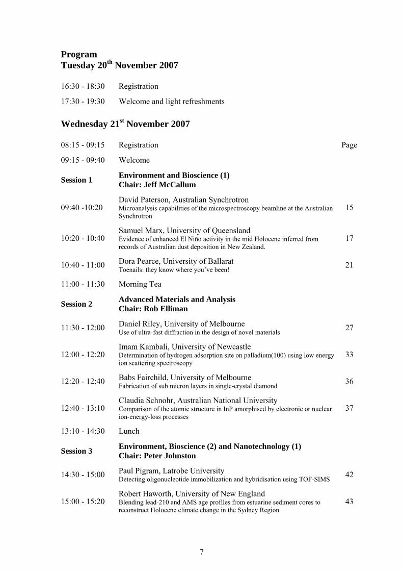
Program Tuesday 20th November 2007
16:30 - 18:30 Registration
17:30 - 19:30 Welcome and light refreshments Wednesday 21st November 2007
08:15 - 09:15 Registration Page
09:15 - 09:40 Welcome
Session 1 Environment and Bioscience (1) Chair: Jeff McCallum
09:40 -10:20 David Paterson, Australian Synchrotron Microanalysis capabilities of the microspectroscopy beamline at the Australian Synchrotron
15
10:20 - 10:40 Samuel Marx, University of Queensland Evidence of enhanced El Niño activity in the mid Holocene inferred from records of Australian dust deposition in New Zealand.
17
10:40 - 11:00 Dora Pearce, University of Ballarat Toenails: they know where you’ve been! 21
11:00 - 11:30 Morning Tea
Session 2 Advanced Materials and Analysis Chair: Rob Elliman
11:30 - 12:00 Daniel Riley, University of Melbourne Use of ultra-fast diffraction in the design of novel materials 27
12:00 - 12:20 Imam Kambali, University of Newcastle Determination of hydrogen adsorption site on palladium(100) using low energy ion scattering spectroscopy
33
12:20 - 12:40 Babs Fairchild, University of Melbourne Fabrication of sub micron layers in single-crystal diamond 36
12:40 - 13:10 Claudia Schnohr, Australian National University Comparison of the atomic structure in InP amorphised by electronic or nuclear ion-energy-loss processes
37
13:10 - 14:30 Lunch
Session 3 Environment, Bioscience (2) and Nanotechnology (1) Chair: Peter Johnston
14:30 - 15:00 Paul Pigram, Latrobe University Detecting oligonucleotide immobilization and hybridisation using TOF-SIMS
42
15:00 - 15:20 Robert Haworth, University of New England Blending lead-210 and AMS age profiles from estuarine sediment cores to reconstruct Holocene climate change in the Sydney Region
43

8
15:20 - 15:40 Andreas Markwitz, GNS Low energy lead implantation into Si for novel group IV nanomaterials 46
15:40 - 16:00 Michael Gladys, University of Newcastle Bridging the gap between the nano-particle and single crystal surface science 50
16:00 - 16:30 Paul Munroe, University of NSW Application of focused ion beam systems to materials analysis 53
16.30 – 18.30 Poster Session 1 and Afternoon Tea
18:00 onwards BBQ
Thursday 22nd November 2007
Session 4 Environment and Bioscience (3) Chair: David Cohen
09:00 - 09:30 James Robertson, AFP Nuclear science and forensic science - complementary sciences! 57
09:30 - 09:50 Serena Abbondante, University of Canberra Radiologically contaminated evidence: extraction procedures and the effect of radioactive materials on forensic DNA profiling
58
09:50 - 10:10 Laura Gladkis, ADFA@UNSW A new methodology in prosthesis research: radioisotope tracing of knee implant wear
60
10:10 - 10:30 Amy Ziebell, University of Wollongong Cylindrical silicon-on-insulator microdosimeter: charge collection characteristics
65
10:30 - 11:00 Julian Adams, Australian Synchrotron Protein crystallography using the Australian Synchrotron 68
11:00 - 11:30 Morning Tea
Session 5 Nanotechnology (2) Chair: Andreas Markwitz
11:30 - 12:00 Matt Kilburn, University of Western Australia NanoSIMS: Recent advances and new applications in SIMS 68
12:00 - 12:20 Damian Carder, GNS Ion-beam sputtered germanium thin films – self-assembly of surface nanostructure using post growth annealing
769
12:20 - 12:40 Michael Dunn, University of Melbourne Interface trap density reduction in thin silicon oxides using ion Implantation
73
12:40 - 13:00 Dinesh Venkatachalam, RMIT Surface fraction statistics of gold nanoclusters of dissimilar sizes determined by RBS
77
9
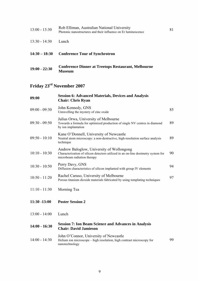
13:00 - 13:30 Rob Elliman, Australian National University Photonic nanostructures and their influence on Er luminescence 81
13:30 - 14:30 Lunch
14:30 – 18:30 Conference Tour of Synchrotron
19:00 - 22:30 Conference Dinner at Treetops Restaurant, Melbourne Museum
Friday 23rd November 2007
09:00 Session 6: Advanced Materials, Devices and Analysis Chair: Chris Ryan
09:00 - 09:30 John Kennedy, GNS Unravelling the mystery of zinc oxide 85
09:30 - 09:50 Julius Orwa, University of Melbourne Towards a formula for optimized production of single NV centres in diamond by ion implantation
89
09:50 - 10:10 Kane O’Donnell, University of Newcastle Neutral atom microscopy: a non-destructive, high-resolution surface analysis technique
89
10:10 - 10:30 Andrew Baloglow, University of Wollongong Characterization of silicon detectors utilized in an on-line dosimetry system for microbeam radiation therapy
90
10:30 - 10:50 Perry Davy, GNS Diffusion characteristics of silicon implanted with group IV elements 94
10:50 - 11:20 Rachel Caruso, University of Melbourne Porous titanium dioxide materials fabricated by using templating techniques 97
11:10 - 11:30 Morning Tea
11:30 -13:00 Poster Session 2
13:00 - 14:00 Lunch
14:00 - 16:30 Session 7: Ion Beam Science and Advances in Analysis Chair: David Jamieson
14:00 - 14:30 John O’Connor, University of Newcastle Helium ion microscope – high resolution, high contrast microscopy for nanotechnology
99

10
14:30 - 14:50 Chris Ryan, CSIRO Next generation x-ray microspectroscopy: towards full-spectral XANES and high throughput fluorescence imaging using massively parallel detector arrays and realtime spectral deconvolution
100
14:50 - 15:10 Michael Went, Australian National University Extended interface analysis using high energy electron scattering 104
15:10 - 15:30 Changyi Yang, University of Melbourne Avalanche detector technology for keV single ion detection and implantation for quantum bits construction
108
15:30 - 15:50 David Cohen, ANSTO Towards a better understanding and prediction of the bremsstrahlung background in PIXE spectra
111
15:50 – 16:10 Andrew Gleadow, University of Melbourne Fully-automated counting of fission tracks in natural minerals for fission track dating and thermochronology
116
16:10 - 16:40 David Belton, CSIRO PIXE imaging of a developing corrosion front beneath a protective coating on galvanized steel
119
16:40 - 17:00 Closing Remarks and Award of Prizes

11
Posters index N. Biluš Abaffy Deposition of high quality metal oxide thin films
using a filtered cathodic vacuum arc 124
A. Alves Detection and placement of single ions in the keV and MeV regimes: MeV ion-aperture scattering 127
K. Belay The effect of annealing temperature on the optical properties of sputter-deposited hafnium oxide thin films 133
John W. Bennett The introduction of the k0-method of neutron activation analysis at ANSTO 136
M. Bhaskaran Investigation of surface crystallites on C54 titanium silicide thin films using transmission electron microscopy 140
Jaroslav Blazek
Structural parameters of wheat starch granules differing in amylose content and functional characteristics studied by small-angle x-ray scattering 143
D. Button The ANSTO ECR ion source and its application to mass spectrometry 147
M. R. J. Carroll Design considerations in the development of magnetic nanoparticles for MRI contrast enhancement 152
C. Chaiwong Plasma immersion ion implantation and deposition of titanium nitride onto polymers 153
C. T. Chang DLTS study of ion and molecular implantation damage in silicon 157
Martin A. Cole Surface modifications of nanoporous alumina membranes by plasma polymerisation 161
Gavin Conibeer Characterisation of nanostructures for photovoltaics 166
M. A. Draganski The refractive index of ion implanted diamond 167
Glenna L. Drisko Metal oxides produced from sol-gel templating of agarose gel applied to vanadium adsorption 168
Daniel W. Drumm Optimisation of Density Functional Theory (DFT) parameters for calculating the electronic and optical properties of diamond. 170
Barbara Etschmann XANES from ROI vs. DA deconvolution of full spectral SXRF data 175
Jing-Hua Fang Fabrication of periodic Al2O3 nanomasks 179
Fang Fang High temperature electronic properties of field-effect transistor based on SiC nanowires 182
V.S. Gill Age mapping of radioisotopes by daughter trace element analysis 185
M. J. Gladys Enantioselectivity of chiral molecules on chiral copper surfaces 189
Sarah K. Hagerty Delineating groundwater flowpaths using 14C dating in the Upper Loddon catchment, central Victoria 195
M. Ionescu ANSTO heavy ion ToF for analysis of light elements in thin films 196
12
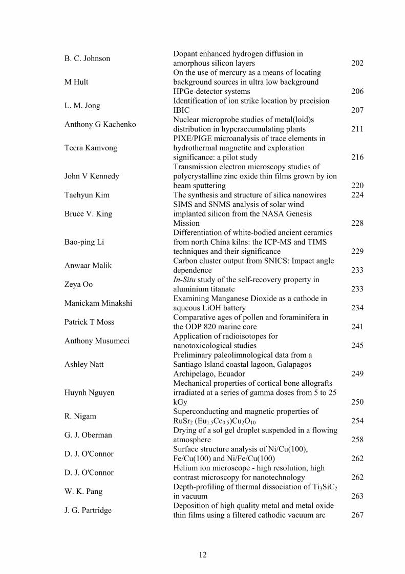
B. C. Johnson Dopant enhanced hydrogen diffusion in amorphous silicon layers 202
M Hult On the use of mercury as a means of locating background sources in ultra low background HPGe-detector systems 206
L. M. Jong Identification of ion strike location by precision IBIC 207
Anthony G Kachenko Nuclear microprobe studies of metal(loid)s distribution in hyperaccumulating plants 211
Teera Kamvong PIXE/PIGE microanalysis of trace elements in hydrothermal magnetite and exploration significance: a pilot study 216
John V Kennedy Transmission electron microscopy studies of polycrystalline zinc oxide thin films grown by ion beam sputtering 220
Taehyun Kim The synthesis and structure of silica nanowires 224
Bruce V. King SIMS and SNMS analysis of solar wind implanted silicon from the NASA Genesis Mission 228
Bao-ping Li Differentiation of white-bodied ancient ceramics from north China kilns: the ICP-MS and TIMS techniques and their significance 229
Anwaar Malik Carbon cluster output from SNICS: Impact angle dependence 233
Zeya Oo In-Situ study of the self-recovery property in aluminium titanate 233
Manickam Minakshi Examining Manganese Dioxide as a cathode in aqueous LiOH battery 234
Patrick T Moss Comparative ages of pollen and foraminifera in the ODP 820 marine core 241
Anthony Musumeci Application of radioisotopes for nanotoxicological studies 245
Ashley Natt Preliminary paleolimnological data from a Santiago Island coastal lagoon, Galapagos Archipelago, Ecuador 249
Huynh Nguyen Mechanical properties of cortical bone allografts irradiated at a series of gamma doses from 5 to 25 kGy 250
R. Nigam Superconducting and magnetic properties of RuSr2 (Eu1.5Ce0.5)Cu2O10 254
G. J. Oberman Drying of a sol gel droplet suspended in a flowing atmosphere 258
D. J. O'Connor Surface structure analysis of Ni/Cu(100), Fe/Cu(100) and Ni/Fe/Cu(100) 262
D. J. O'Connor Helium ion microscope - high resolution, high contrast microscopy for nanotechnology 262
W. K. Pang Depth-profiling of thermal dissociation of Ti3SiC2 in vacuum 263
J. G. Partridge Deposition of high quality metal and metal oxide thin films using a filtered cathodic vacuum arc 267
13
J.R. Prescott Thermoluminescence spectra of quartz from single crystals 268
Daniel Pyke Raman measurements of hydrogen ions implanted into silicon 272
Daniel Pyke Hydrogen refinement during solid phase epitaxial crystallisation of buried amorphous silicon layers 276
M. Raiber Application of environmental isotopes to study aquifer interactions and their impact on groundwater salinisation in western Victoria 282
A.B.Rosenfeld Investigation of monolithic Si ∆E-E telescope using IBIC and application for radiobiological efficiency estimation in proton therapy 283
Y M Sabri Gold nano-structures electroplated on au electrodes of quartz crystal microbalance (QCM) for enhanced mercury vapour sensitivity 287
R. Siegele Localisation of trace metals in hyper-accumulating plants using µ-PIXE 292
Vijay Sivan Wafer scale etching of lithium niobate using conventional diffusion process 296
Michael Smith Establishment of efficiency function for the gamma-ray spectrometry system 296
Paul Spizzirri A TEM study of Si-SiO2 interfaces in silicon nanodevices 297
Paul Spizzirri Characterisation of high quality, thermally grown silicon dioxide on silicon 301
Paul Spizzirri An EPR study on the activation of low energy phosphorus ions implanted into silicon 305
S. Sriram Modified unit cell of preferentially oriented strontium-doped lead zirconate titanate thin films on Pt/TiO2/Si 310
Alexander M. St John Separation of uranium using polymer inclusion membranes 314
Eduard Stelcer Ion beam analysis and positive matrix factorisation modeling: tools for exploring aerosol source fingerprints 318
Jessica A. van Donkelaar Single ion implantation using nano-apertures: precision placement for CTAP 322
L. Velleman Template fabricated gold nanotubes membranes: a nucleation and growth study 326
Dinesh Kumar Venkatachalam Surface fraction statistics of gold nanoclusters of dissimilar sizes determined by RBS 330
Byron J. Villis A low energy, angle dependent, defect study of H implanted Si 334
Xingdong Wang Synthesis, characterization and photocatalytic application of porous Au/TiO2 nano-hybrids 338
J.L. Wang Magnetic phase transitions in PrMn2-xFexGe2 342
Mark Thomas Warne History of natural environmental events in a pristine estuary: ostracod proxies and 210Pb chronology from Wingan Inlet, Victoria 344
A-M. M. Williams Iron deposition in archaeological teeth 348

14
Myint Zaw Oxidation profiles of arsenic, iron, manganese and uranium in tailings dam samples using x-ray absorption near-edge structure spectroscopy 352
Waven Zhang Reduction of titanium dioxide: comparison of analysis by Raman spectroscopy and XRD 358
B. Zorko Measurement of actinides by the unfocused beam AMS 363

301
Characterisation of high quality, thermally grown silicon dioxide on silicon
Paul G. Spizzirri 1, Jeff McCallum 1, Michael Dunn1, Eric Gauja 2 Steven Prawer 1 1Centre of Excellence for Quantum Computer Technology, School of Physics, University of
Melbourne, Melbourne, Victoria, 3010. 2Centre of Excellence for Quantum Computer Technology, School of Physics, University of
New South Wales, Sydney, New South Wales, 2052.
Abstract
High quality thermal oxides, as used to provide electrical insulation in MOS devices, underpin the Si:P solid state charge qubit readout architectures. Establishing oxide growth conditions and implantation and annealing parameters that result in suitably low trap/defect concentrations is vital to qubit integrity. However, characterising oxides with thicknesses around 5nm can be challenging. In this work, we describe the use of spectroscopic ellipsometry and deep level transient spectroscopy (DLTS) to study the oxide thickness and uniformity as well as interface trap state densities (Dit’s) using both exposed and encapsulated MOS capacitor test structures.
Introduction
Fabrication of a silicon based, solid state quantum computer (QC) requires precise positioning of dopant atoms, each registered to an electronic gate, in a low defect density environment close enough to a surface or interface to allow independent gate operations to be performed. This low dopant-density, near-surface regime presents challenges for analysis including: measurement of the quality of materials and their interfaces, growth of high-quality (gate) oxides and observation of ion implantation-induced damage. Here, we introduce the techniques we have used to address some of these materials related issues. Spectroscopic ellipsometry (SE) and deep level transient spectroscopy (DLTS) were applied to the characterization of thermal oxides fabricated in this Centre.
Deep level transient spectroscopy (DLTS) and its constant capacitance variant (CC-DLTS) offer a sensitive means of identifying and quantifying the bulk charge traps and interface states introduced by ion implantation. It can also be used to evaluate processing by providing a means of monitoring the trap formation and removal during subsequent annealing steps. Of particular importance to the QC program is its ability to probe the near oxide interface of metal-oxide-semiconductor (MOS) devices with adequate sensitivity to detect defects in the ion fluence regime of 1011cm-2 of interest.
CC-DLTS differs from regular DLTS in that instead of monitoring the capacitance transient arising from trap emission, the gate voltage is adjusted so that a constant capacitance is maintained throughout the emission phase. The variation in the gate voltage is then related to the number of defects which emit electrons. Implantation and oxidation processes give rise to the formation of charge traps at the SiO2/Si interface and also within the Si bulk. These defects can be detected using MOS capacitor structures
An alternative method for characterizing thin oxide films with sub nanometer precision is ellipsometry. This is an optical technique which measures the change in the polarization state of light reflected from the surface of a sample. The measured values are expressed as Ψ and ∆. These values are related to the ratio of Fresnel reflection coefficients, Rp and Rs, for p and s-polarized light, respectively. Because ellipsometry measures the ratio of two values, it can be highly accurate and very
302
reproducible. The technique can also be performed with variable excitation wavelength and angle. In this way, an optical model can be deduced based upon the following sample properties: film thickness, material optical constants, surface roughness and composition. It is a rapid measurement that is non-destructive and can be performed on relatively small areas (50µm x 150µm).
In this work, we describe the application of these two techniques to the measurement of thermally grown, high quality gate oxides which are used for MOS devices. Their routine characterization is important to ensure consistency in device fabrication. In addition, given that both electrical and morphological properties of these oxides can impact on the successful operation of a QC device, these measurements provide a quality control framework for process troubleshooting.
Experimental Details
Thermally grown, device quality (gate) oxides were fabricated in a quartz, triple wall, multi-zone furnace (UNSW) under oxygen with subsequent passivation. Field (wet) oxides were also thermally grown and used for device isolation (as used in encapsulated geometries). Point contact and encapsulated MOS capacitors were fabricated using conventional photolithographic techniques.
A variable temperature, SULA Deep Level Transient Spectroscopy system (DLTS) was used to perform electrical characterization of the oxides in a point contact or encapsulated MOS capacitor configuration. The measured density of interface trap states (Dit) is reported near the band edge.
Oxide thicknesses were measured using a Jobin Yvon spectroscopic ellipsometer (SE). Measurements were taken from 250nm – 620nm (using 4nm steps) at an angle of incidence of 70 degrees. Wafer pieces (2” wafer quarters) with a grown thermal oxide layer were analysed using a 3mm x 1mm spot.
Results and Discussion
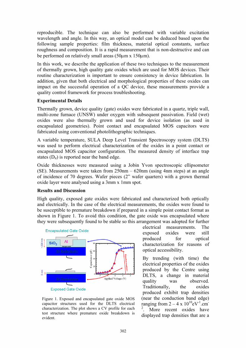
High quality, exposed gate oxides were fabricated and characterized both optically and electrically. In the case of the electrical measurements, the oxides were found to be susceptible to premature breakdown if prepared in a simple point contact format as shown in Figure 1. To avoid this condition, the gate oxide was encapsulated where they were subsequently found to be stable so this arrangement was adopted for further
electrical measurements. The exposed oxides were still produced for optical characterization for reasons of optical accessibility.
By trending (with time) the electrical properties of the oxides produced by the Centre using DLTS, a change in material quality was observed. Traditionally, the oxides produced exhibit trap densities
(near the conduction band edge) ranging from 2 – 4 x 10¹⁰eV-1.cm-
2. More recent oxides have displayed trap densities that are a
Figure 1. Exposed and encapsulated gate oxide MOS capacitor structures used for the DLTS electrical characterization. The plot shows a CV profile for each test structure where premature oxide breakdown is evident.

303
of six higher (i.e. 1 – 3 x 10¹¹eV-1.cm-2). The plot in Figure 2 shows a comparison of these two oxide result extremes overlaid.
Given the significant difference in Dit for these two batches, further investigation of the cause of the reduced oxide quality was undertaken. Spectroscopic ellipsometry was performed on exposed gate oxides from the same batch to determine if there was a change in the SiO2 layer thickness or composition. The plot in Figure 3 shows the data and a model fit to a Si-SiO2 system where IS and IC are related to the
ellipsometric angle Ψ and ∆. The quality of the model fit to the data indicates that it is appropriate for this system.
The ellipsometric analysis of the gate oxides was performed on larger samples (wafer quarters) which allowed sub-sampling to profile the oxide uniformity. An example of the resultant profile is shown in Figure 4 where there is a clear trend towards thicker oxides at the top corner of the wafer. The thickness of the oxide observed on the bad batches is significantly larger than the target thickness (5nm) suggesting that there is an uncontrolled oxide growth step in the process. Also significant is the location on the wafer of the thickest oxide as this repeatedly occurred on that part of the substrate which was not in contact with the furnace quartz boat. This boat is used to hold the sample during the oxidation process and it clearly influences the oxidation rate when wafers are in contact with it.
Conclusions
The two techniques described in this work generally target unrelated materials problems however here, they have provided complementary information that has facilitated the troubleshooting of a nano-fabrication process; the growth of ultra-thin oxide films on silicon. While the changes observed in the oxide properties
Figure 2. Trap density plots overlaid for a good oxide and an oxide from a bad batch.
Figure 3. Spectroscopic ellipsometry measurement of Si-SiO2 showing a plot of IS vs IC with raw data and model fit overlaid.
Figure 3. SiO2 thickness profile across a wafer quarter that has an exposed (thermal) gate oxide with a target thickness of ~5nm. The error of the reported results is ±0.1nm.

304
for different batches appear to be significant (i.e. a 50% increase in the target oxide thickness and six times the Dit values), they can arise from just a 1 ppm change in process gas contamination levels during the processing of the substrates. Identifying such a small change requires techniques capable of rapid feedback (preferably on-line) and high sensitivity to the relevant material properties. Clearly, these two techniques used in this work are well suited to the investigation of this problem. The outcomes of this work have resulted in significant upgrades to some of the processes including key infrastructure responsible for oxide growth in the Centre. There is a clear need for ongoing measurements of this kind for process control in laboratories performing silicon semiconductor fabrication.
Acknowledgements
The work is funded by the Australian Research Council, the Australian Government and US Army Research Office under Contract No. W911NF-04-1-0290.
305
An EPR study on the activation of low energy phosphorus ions implanted into silicon
Paul Spizzirri 1, Jeff McCallum 1, 2Wayne Hutchison 2, Nakorn Suwuntanasarn 2
Natasa Bulatovic, Nikolas Stavrias and Steven Prawer 1 1Centre of Excellence for Quantum Computer Technology, School of Physics, University of
Melbourne, Melbourne, VIC, 3010. 2Centre of Excellence for Quantum Computer Technology, School of PEMS, University of
New South Wales@ADFA, Canberra, ACT, 2600.
Abstract
The use of low energy ion implantation techiques for the “Top-Down” fabrication of a Si:P solid state qubit relies upon efficient dopant activation that is not dependent upon the incident ion energy (i.e. resultant ion depth). Issues such as: dopant activation, gettering at the silicon interface and ionization by interfacial trap states could all impact upon the successful fabrication and operation of such a device. In this work, we report on the application of semi-quantitative EPR to measurements of phosphorus ensembles that have been implanted (with subsequent RTA annealing) using various implantation energies. Using the characteristic EPR spectral lines (and intensities for quantitation) to identify the phosphorus dopants and radicals (e.g. Pb) which may constitute electronic trap states, we will discuss the results in the context of optimising qubit fabrication and measurement.
Introduction
In the “Top Down” approach to the fabrication of a solid state, phosphorus in silicon (Si:P) quantum computer (QC), low energy ion beams are used to position individual phosphorus atoms in silicon with precision alignment to MOS readout architectures. The use of low energy ion beams for the fabrication of QC devices is highly desirable as it provides a means of reducing the straggle, a parameter which normally results in reduced positional accuracy, in the placement of the dopant atom.
Implanting ions at very low energies may appear to be an attractive means of achieving accurate dopant placement however surface layers, particularly silicon dioxide (SiO2), impose a lower energy limit of ~10keV. The reason for this becomes apparent if we consider the percentage of incident ions that remain in the top oxide layer as we reduce the incident ion energy. This is depicted graphically in Figure 1 where SRIM simulations [1] have been used to quantify this loss (%) for low energy, molecular phosphorus ions (P2) into silicon with a 5nm surface oxide (SiO2) layer.
Once implanted, dopant ions are activated thermally (i.e. annealed). While there are a number of techniques available for determining whether dopants have been
Figure 1. Simulated loss (%) of donors to a 5nm surface oxide when implanting into silicon using a low energy, molecular phosphorus (P2) ion beam.
306
effectively activated in semiconductors, they do not work well for low fluence, shallow (i.e. near surface) implanted layers in intrinsic silicon. Electron paramagnetic resonance (EPR) spectroscopy is one technique that is well suited to the measurement of phosphorus ensembles as it has a low detection limit (approaching 1010 spins/cm3), can be used semi-quantitatively to estimate the (active) doping concentration, can be used to identify dopants and some trap states spectroscopically and is sensitive to the interactions of neighboring nuclear spins which result in hyperfine splittings. For this reason, we have applied this technique to the study of ion implanted phosphorus to investigate dopant activation as a function of ion energy, the generation of trap states and to observe changes in donor-donor interactions as a function of fluence.
Experimental Details
Low energy ion implantation was performed using a 150keV implanter (Australian National University) or a 15keV Colutron implanter (University of Melbourne) into intrinsic silicon (<100>, >4 kΩ.cm) with either a native oxide (~2nm) or thermally grown oxide (~5nm). Samples were cleaned using standard Piranha/RCA wet chemical processes. For studies of ion loss to surface oxides, substrates were prepared without an SiO2 surface layer by chemically etching the oxide and hydrogenating the resultant interface. In this case, these samples were implanted off axis (8 degrees) to prevent channeling. All implanted samples underwent rapid thermal annealing (RTA) at 1050°C for 5s.
The electron paramagnetic resonance (EPR) experiments were carried out using a Bruker ESP300 spectrometer with a standard x-band cavity coupled to an Oxford instruments flow cryostat allowing measurements down to ~5 K (Australian National University). Si:P samples, typically wafers of 5 x 10mm, were inserted to the cavity on the end of a silica glass rod. A field sweep of width 0.01T (100G) about a centre field of 0.3380 T (3380 G) was employed. For Si:P, g = 1.99875 ± 0.00010 [2], so the
P donor hyperfine split doublet EPR lines were placed symmetrically about this centre field with a typical microwave frequency of ~9.45GHz. For natural silicon, the typical linewidths of individual sub-resonances are several gauss and so a field modulation amplitude of ± 2.0G is used to give maximum signal without additional line broadening. The long spin-lattice relaxation rates at close to 5K [3] in the dark for Si:P are not conducive to timely slow passage measurements. With white light from a halogen lamp focused into the cavity, the spin-lattice relaxation is shortened considerably by interaction with unpolarised photo-electrons and the slow passage experiment can proceed.
Results and Discussion
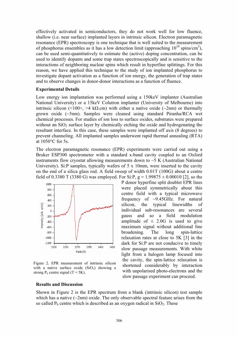
Shown in Figure 2 is the EPR spectrum from a blank (intrinsic silicon) test sample which has a native (~2nm) oxide. The only observable spectral feature arises from the so called Pb centre which is described as an oxygen radical in SiO2. These
Figure 2. EPR measurement of intrinsic silicon with a native surface oxide (SiO2) showing a strong Pb centre signal (T = 5K).
307
oxygen defects form naturally during the uncontrolled growth of the native oxide and are known to be electrically active. Indeed, it has been shown that they are amphoteric as they have 2 allowed energy levels in the Si-SiO2 bandgap corresponding to a positive and negative charge state. When these traps are populated, they can alter the threshold voltage of MOSFETs so ideally, they should be avoided in any device.
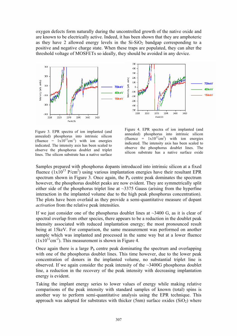
Samples prepared with phosphorus dopants introduced into intrinsic silicon at a fixed fluence (1x10¹³ P/cm2) using various implantation energies have their resultant EPR spectrum shown in Figure 3. Once again, the Pb centre peak dominates the spectrum however, the phosphorus doublet peaks are now evident. They are symmetrically split either side of the phosphorus triplet line at ~3375 Gauss (arising from the hyperfine interaction in the implanted volume due to the high peak phosphorus concentration). The plots have been overlaid as they provide a semi-quantitative measure of dopant activation from the relative peak intensities.
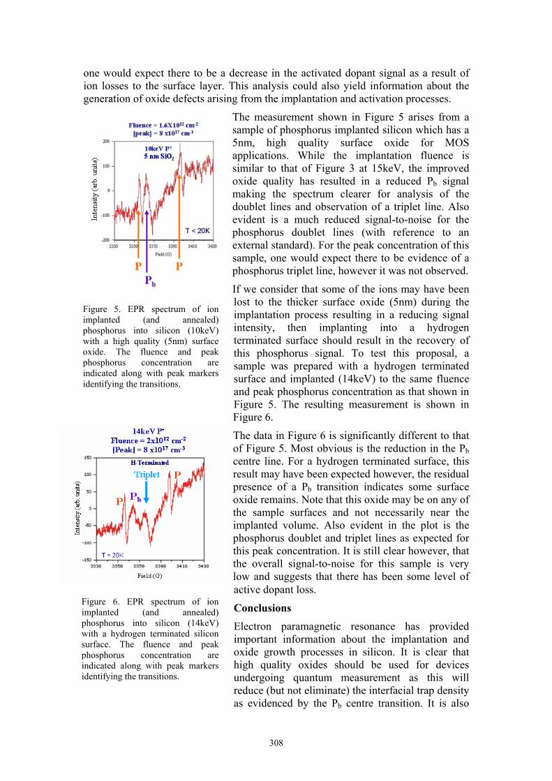
If we just consider one of the phosphorus doublet lines at ~3400 G, as it is clear of spectral overlap from other species, there appears to be a reduction in the doublet peak intensity associated with reduced implantation energy; the most pronounced result being at 15keV. For comparison, the same measurement was performed on another sample which was implanted and processed in the same way but at a lower fluence (1x1012cm-2). This measurement is shown in Figure 4.
Once again there is a large Pb centre peak dominating the spectrum and overlapping with one of the phosphorus doublet lines. This time however, due to the lower peak concentration of donors in the implanted volume, no substantial triplet line is observed. If we again consider the peak intensity of the ~3400G phosphorus doublet line, a reduction in the recovery of the peak intensity with decreasing implantation energy is evident.
Taking the implant energy series to lower values of energy while making relative comparisons of the peak intensity with standard samples of known (total) spins is another way to perform semi-quantitative analysis using the EPR technique. This approach was adopted for substrates with thicker (5nm) surface oxides (SiO2) where
Figure 3. EPR spectra of ion implanted (and annealed) phosphorus into intrinsic silicon (fluence = 1x1013cm-2) with ion energies indicated. The intensity axis has been scaled to observe the phosphorus doublet and triplet lines. The silicon substrate has a native surface
Figure 4. EPR spectra of ion implanted (and annealed) phosphorus into intrinsic silicon (fluence = 1x1012cm2) with ion energies indicated. The intensity axis has been scaled to observe the phosphorus doublet lines. The silicon substrate has a native surface oxide
308
one would expect there to be a decrease in the activated dopant signal as a result of ion losses to the surface layer. This analysis could also yield information about the generation of oxide defects arising from the implantation and activation processes.
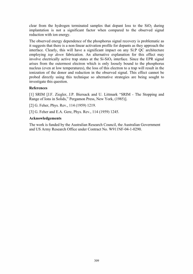
The measurement shown in Figure 5 arises from a sample of phosphorus implanted silicon which has a 5nm, high quality surface oxide for MOS applications. While the implantation fluence is similar to that of Figure 3 at 15keV, the improved oxide quality has resulted in a reduced Pb signal making the spectrum clearer for analysis of the doublet lines and observation of a triplet line. Also evident is a much reduced signal-to-noise for the phosphorus doublet lines (with reference to an external standard). For the peak concentration of this sample, one would expect there to be evidence of a phosphorus triplet line, however it was not observed.
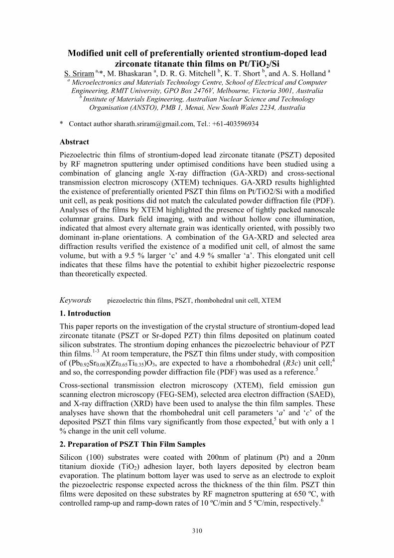
If we consider that some of the ions may have been lost to the thicker surface oxide (5nm) during the implantation process resulting in a reducing signal intensity, then implanting into a hydrogen terminated surface should result in the recovery of this phosphorus signal. To test this proposal, a sample was prepared with a hydrogen terminated surface and implanted (14keV) to the same fluence and peak phosphorus concentration as that shown in Figure 5. The resulting measurement is shown in Figure 6.
The data in Figure 6 is significantly different to that of Figure 5. Most obvious is the reduction in the Pb centre line. For a hydrogen terminated surface, this result may have been expected however, the residual presence of a Pb transition indicates some surface oxide remains. Note that this oxide may be on any of the sample surfaces and not necessarily near the implanted volume. Also evident in the plot is the phosphorus doublet and triplet lines as expected for this peak concentration. It is still clear however, that the overall signal-to-noise for this sample is very low and suggests that there has been some level of active dopant loss.
Conclusions
Electron paramagnetic resonance has provided important information about the implantation and oxide growth processes in silicon. It is clear that high quality oxides should be used for devices undergoing quantum measurement as this will reduce (but not eliminate) the interfacial trap density as evidenced by the Pb centre transition. It is also
Figure 6. EPR spectrum of ion implanted (and annealed) phosphorus into silicon (14keV) with a hydrogen terminated silicon surface. The fluence and peak phosphorus concentration are indicated along with peak markers identifying the transitions.
Figure 5. EPR spectrum of ion implanted (and annealed) phosphorus into silicon (10keV) with a high quality (5nm) surface oxide. The fluence and peak phosphorus concentration are indicated along with peak markers identifying the transitions.
309
clear from the hydrogen terminated samples that dopant loss to the SiO2 during implantation is not a significant factor when compared to the observed signal reduction with ion energy.
The observed energy dependence of the phosphorus signal recovery is problematic as it suggests that there is a non-linear activation profile for dopants as they approach the interface. Clearly, this will have a significant impact on any Si:P QC architecture employing top down fabrication. An alternative explanation for this effect may involve electrically active trap states at the Si-SiO2 interface. Since the EPR signal arises from the outermost electron which is only loosely bound to the phosphorus nucleus (even at low temperatures), the loss of this electron to a trap will result in the ionization of the donor and reduction in the observed signal. This effect cannot be probed directly using this technique so alternative strategies are being sought to investigate this question.
References
[1] SRIM [J.F. Ziegler, J.P. Biersack and U. Littmark “SRIM - The Stopping and Range of Ions in Solids,” Pergamon Press, New York, (1985)].
[2] G. Feher, Phys. Rev., 114 (1959) 1219.
[3] G. Feher and E.A. Gere, Phys. Rev., 114 (1959) 1245.
Acknowledgements
The work is funded by the Australian Research Council, the Australian Government and US Army Research Office under Contract No. W911NF-04-1-0290.
310
Modified unit cell of preferentially oriented strontium-doped lead zirconate titanate thin films on Pt/TiO2/Si
S. Sriram a,*, M. Bhaskaran a, D. R. G. Mitchell b, K. T. Short b, and A. S. Holland a a Microelectronics and Materials Technology Centre, School of Electrical and Computer
Engineering, RMIT University, GPO Box 2476V, Melbourne, Victoria 3001, Australia b Institute of Materials Engineering, Australian Nuclear Science and Technology
Organisation (ANSTO), PMB 1, Menai, New South Wales 2234, Australia
* Contact author [email protected], Tel.: +61-403596934 Abstract
Piezoelectric thin films of strontium-doped lead zirconate titanate (PSZT) deposited by RF magnetron sputtering under optimised conditions have been studied using a combination of glancing angle X-ray diffraction (GA-XRD) and cross-sectional transmission electron microscopy (XTEM) techniques. GA-XRD results highlighted the existence of preferentially oriented PSZT thin films on Pt/TiO2/Si with a modified unit cell, as peak positions did not match the calculated powder diffraction file (PDF). Analyses of the films by XTEM highlighted the presence of tightly packed nanoscale columnar grains. Dark field imaging, with and without hollow cone illumination, indicated that almost every alternate grain was identically oriented, with possibly two dominant in-plane orientations. A combination of the GA-XRD and selected area diffraction results verified the existence of a modified unit cell, of almost the same volume, but with a 9.5 % larger ‘c’ and 4.9 % smaller ‘a’. This elongated unit cell indicates that these films have the potential to exhibit higher piezoelectric response than theoretically expected.
Keywords piezoelectric thin films, PSZT, rhombohedral unit cell, XTEM
1. Introduction
This paper reports on the investigation of the crystal structure of strontium-doped lead zirconate titanate (PSZT or Sr-doped PZT) thin films deposited on platinum coated silicon substrates. The strontium doping enhances the piezoelectric behaviour of PZT thin films.1-3 At room temperature, the PSZT thin films under study, with composition of (Pb0.92Sr0.08)(Zr0.65Ti0.35)O3, are expected to have a rhombohedral (R3c) unit cell;4 and so, the corresponding powder diffraction file (PDF) was used as a reference.5
Cross-sectional transmission electron microscopy (XTEM), field emission gun scanning electron microscopy (FEG-SEM), selected area electron diffraction (SAED), and X-ray diffraction (XRD) have been used to analyse the thin film samples. These analyses have shown that the rhombohedral unit cell parameters ‘a’ and ‘c’ of the deposited PSZT thin films vary significantly from those expected,5 but with only a 1 % change in the unit cell volume.
2. Preparation of PSZT Thin Film Samples
Silicon (100) substrates were coated with 200nm of platinum (Pt) and a 20nm titanium dioxide (TiO2) adhesion layer, both layers deposited by electron beam evaporation. The platinum bottom layer was used to serve as an electrode to exploit the piezoelectric response expected across the thickness of the thin film. PSZT thin films were deposited on these substrates by RF magnetron sputtering at 650 ºC, with controlled ramp-up and ramp-down rates of 10 ºC/min and 5 ºC/min, respectively.6
311
3. Results and Discussion
3.1. Cross-Sectional Imaging
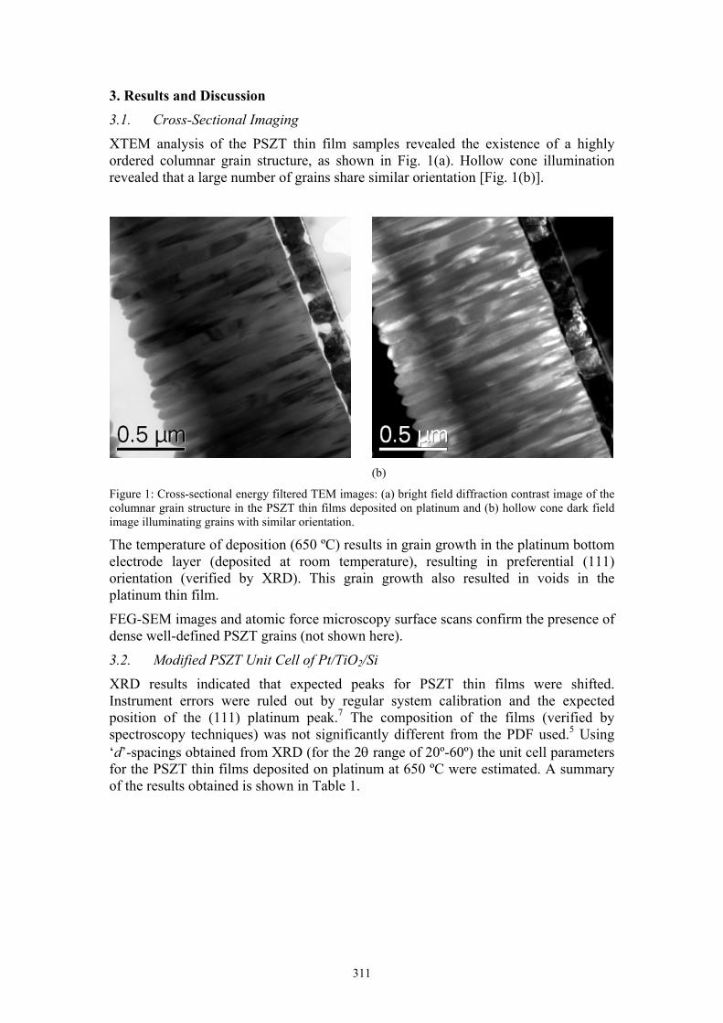
XTEM analysis of the PSZT thin film samples revealed the existence of a highly ordered columnar grain structure, as shown in Fig. 1(a). Hollow cone illumination revealed that a large number of grains share similar orientation [Fig. 1(b)].
(b)
Figure 1: Cross-sectional energy filtered TEM images: (a) bright field diffraction contrast image of the columnar grain structure in the PSZT thin films deposited on platinum and (b) hollow cone dark field image illuminating grains with similar orientation.
The temperature of deposition (650 ºC) results in grain growth in the platinum bottom electrode layer (deposited at room temperature), resulting in preferential (111) orientation (verified by XRD). This grain growth also resulted in voids in the platinum thin film.
FEG-SEM images and atomic force microscopy surface scans confirm the presence of dense well-defined PSZT grains (not shown here).
3.2. Modified PSZT Unit Cell of Pt/TiO2/Si
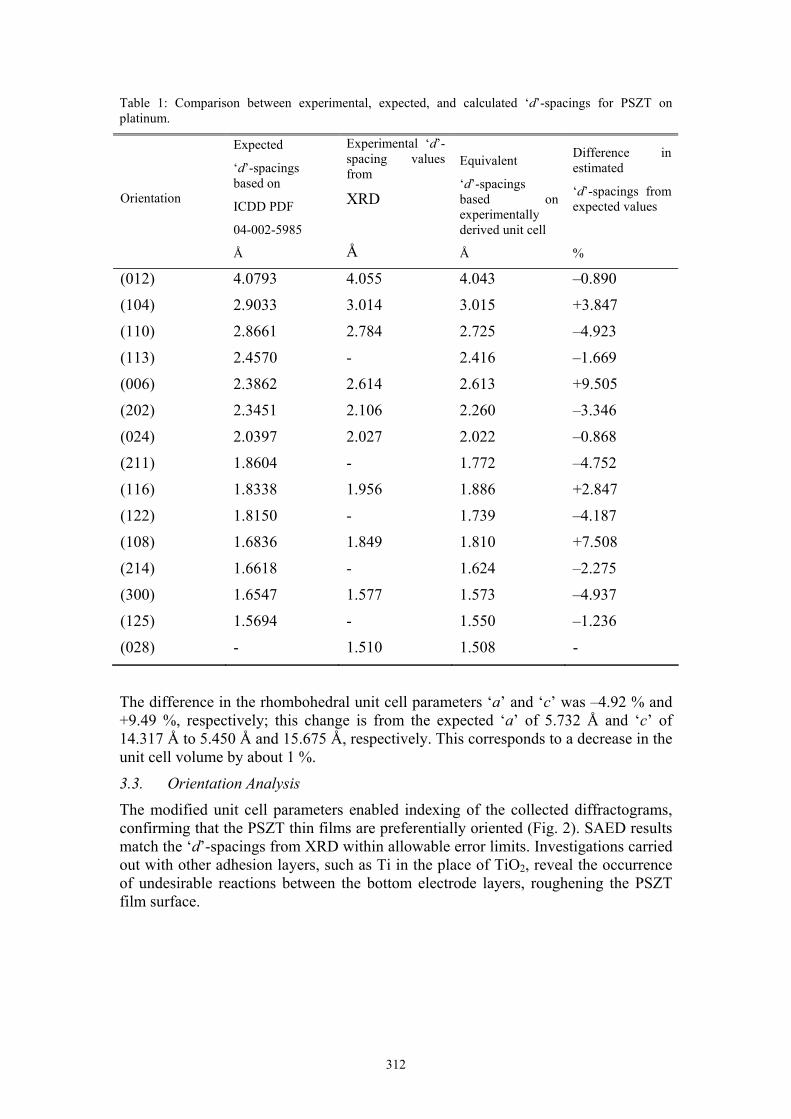
XRD results indicated that expected peaks for PSZT thin films were shifted. Instrument errors were ruled out by regular system calibration and the expected position of the (111) platinum peak.7 The composition of the films (verified by spectroscopy techniques) was not significantly different from the PDF used.5 Using ‘d’-spacings obtained from XRD (for the 2θ range of 20º-60º) the unit cell parameters for the PSZT thin films deposited on platinum at 650 ºC were estimated. A summary of the results obtained is shown in Table 1.
312
Table 1: Comparison between experimental, expected, and calculated ‘d’-spacings for PSZT on platinum.
Orientation
Expected
‘d’-spacings based on
ICDD PDF
04-002-5985
Å
Experimental ‘d’-spacing values from
XRD
Å
Equivalent
‘d’-spacings based on experimentally derived unit cell
Å
Difference in estimated
‘d’-spacings from expected values
%
(012) 4.0793 4.055 4.043 –0.890
(104) 2.9033 3.014 3.015 +3.847
(110) 2.8661 2.784 2.725 –4.923
(113) 2.4570 - 2.416 –1.669
(006) 2.3862 2.614 2.613 +9.505
(202) 2.3451 2.106 2.260 –3.346
(024) 2.0397 2.027 2.022 –0.868
(211) 1.8604 - 1.772 –4.752
(116) 1.8338 1.956 1.886 +2.847
(122) 1.8150 - 1.739 –4.187
(108) 1.6836 1.849 1.810 +7.508
(214) 1.6618 - 1.624 –2.275
(300) 1.6547 1.577 1.573 –4.937
(125) 1.5694 - 1.550 –1.236
(028) - 1.510 1.508 -
The difference in the rhombohedral unit cell parameters ‘a’ and ‘c’ was –4.92 % and +9.49 %, respectively; this change is from the expected ‘a’ of 5.732 Å and ‘c’ of 14.317 Å to 5.450 Å and 15.675 Å, respectively. This corresponds to a decrease in the unit cell volume by about 1 %.
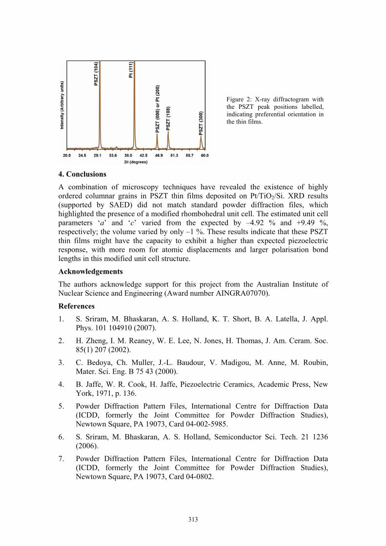
3.3. Orientation Analysis
The modified unit cell parameters enabled indexing of the collected diffractograms, confirming that the PSZT thin films are preferentially oriented (Fig. 2). SAED results match the ‘d’-spacings from XRD within allowable error limits. Investigations carried out with other adhesion layers, such as Ti in the place of TiO2, reveal the occurrence of undesirable reactions between the bottom electrode layers, roughening the PSZT film surface.
313
4. Conclusions
A combination of microscopy techniques have revealed the existence of highly ordered columnar grains in PSZT thin films deposited on Pt/TiO2/Si. XRD results (supported by SAED) did not match standard powder diffraction files, which highlighted the presence of a modified rhombohedral unit cell. The estimated unit cell parameters ‘a’ and ‘c’ varied from the expected by –4.92 % and +9.49 %, respectively; the volume varied by only –1 %. These results indicate that these PSZT thin films might have the capacity to exhibit a higher than expected piezoelectric response, with more room for atomic displacements and larger polarisation bond lengths in this modified unit cell structure.
Acknowledgements
The authors acknowledge support for this project from the Australian Institute of Nuclear Science and Engineering (Award number AINGRA07070).
References
1. S. Sriram, M. Bhaskaran, A. S. Holland, K. T. Short, B. A. Latella, J. Appl. Phys. 101 104910 (2007).
2. H. Zheng, I. M. Reaney, W. E. Lee, N. Jones, H. Thomas, J. Am. Ceram. Soc. 85(1) 207 (2002).
3. C. Bedoya, Ch. Muller, J.-L. Baudour, V. Madigou, M. Anne, M. Roubin, Mater. Sci. Eng. B 75 43 (2000).
4. B. Jaffe, W. R. Cook, H. Jaffe, Piezoelectric Ceramics, Academic Press, New York, 1971, p. 136.
5. Powder Diffraction Pattern Files, International Centre for Diffraction Data (ICDD, formerly the Joint Committee for Powder Diffraction Studies), Newtown Square, PA 19073, Card 04-002-5985.
6. S. Sriram, M. Bhaskaran, A. S. Holland, Semiconductor Sci. Tech. 21 1236 (2006).
7. Powder Diffraction Pattern Files, International Centre for Diffraction Data (ICDD, formerly the Joint Committee for Powder Diffraction Studies), Newtown Square, PA 19073, Card 04-0802.
Figure 2: X-ray diffractogram with the PSZT peak positions labelled, indicating preferential orientation in the thin films.
314
Separation of uranium using polymer inclusion membranes Alexander M. St John a*, Spas D. Kolev a,, Robert W. Cattralla,c, Jilska M. Pererab,
Long D. Nghiemd and Karin H. Soldenhoffe a School of Chemistry, The University of Melbourne, Victoria 3010 Australia
b Department of Chemical and Biomolecular Engineering, The University of Melbourne, Victoria 3010 Australia
c Department of Chemistry, La Trobe University, Victoria 3086 Australia d School of Civil, Mining and Environmental Engineering, University of Wollongong, NSW 2252
Australia e ANSTO Minerals, Lucas Heights NSW 2234 Australia
* Corresponding Author: [email protected]
Polymer Inclusion Membrane (PIM) techniques have shown potential for separation of metal ions from their dilute solutions and are cheap and simple to manufacture. In this study, the PIM technique has been applied to the separation of uranium from dilute aqueous solutions. It is thought that the technique might be used to efficiently remove uranium from solutions contaminated with low-levels of uranium, such as effluent from milling processes.
PIMs usually consist of an extraction reagent (or extractant), entrapped within a polymer matrix. Plasticizers and/or modifiers may also be present to enhance mechanical or chemical properties of the membranes. The great advantage of PIMs over conventional liquid-liquid extraction techniques (more commonly referred to as solvent extraction (SX)) is that extractants which are generally hazardous substances, both to humans and the environment, are wholly contained within the polymer matrix and the need for large inventories of often toxic and flammable diluents is greatly reduced. However, due to the increased diffusive resistance within PIMs, the flux of species across the membrane is much poorer compared to SX. 1
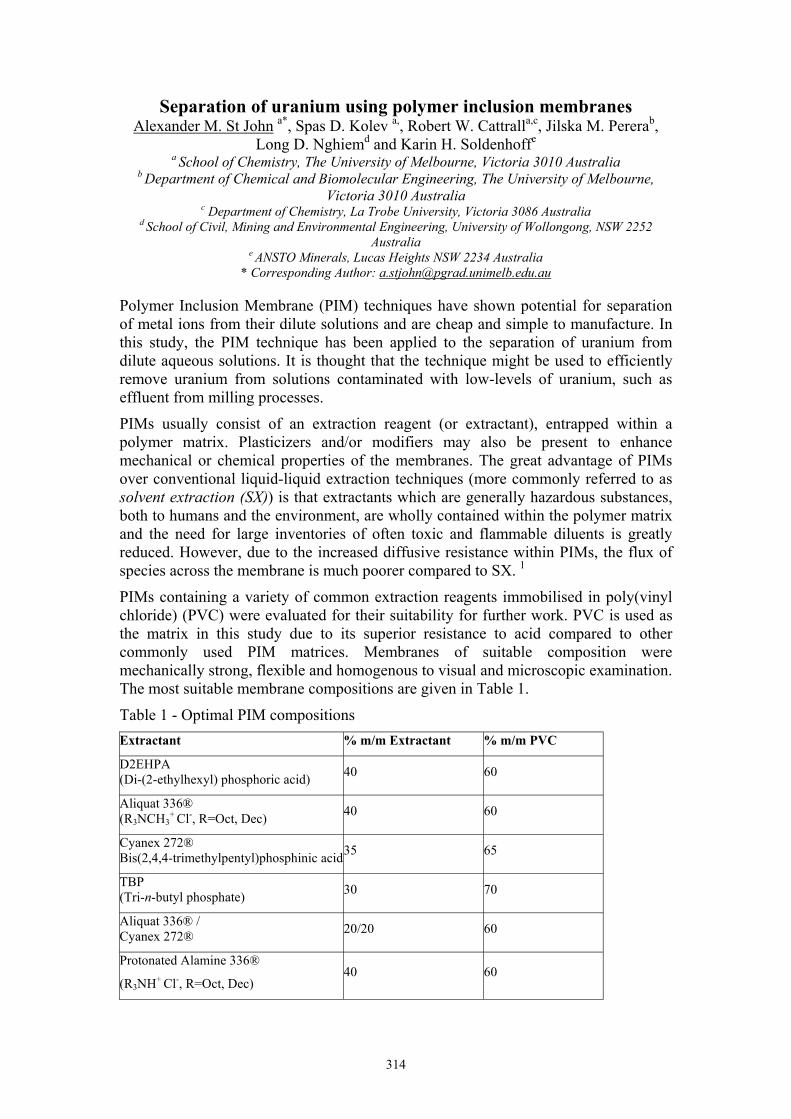
PIMs containing a variety of common extraction reagents immobilised in poly(vinyl chloride) (PVC) were evaluated for their suitability for further work. PVC is used as the matrix in this study due to its superior resistance to acid compared to other commonly used PIM matrices. Membranes of suitable composition were mechanically strong, flexible and homogenous to visual and microscopic examination. The most suitable membrane compositions are given in Table 1.
Table 1 - Optimal PIM compositions Extractant % m/m Extractant % m/m PVC
D2EHPA (Di-(2-ethylhexyl) phosphoric acid) 40 60
Aliquat 336® (R3NCH3
+ Cl-, R=Oct, Dec) 40 60
Cyanex 272® Bis(2,4,4-trimethylpentyl)phosphinic acid35 65
TBP (Tri-n-butyl phosphate) 30 70
Aliquat 336® / Cyanex 272® 20/20 60
Protonated Alamine 336®
(R3NH+ Cl-, R=Oct, Dec) 40 60
315
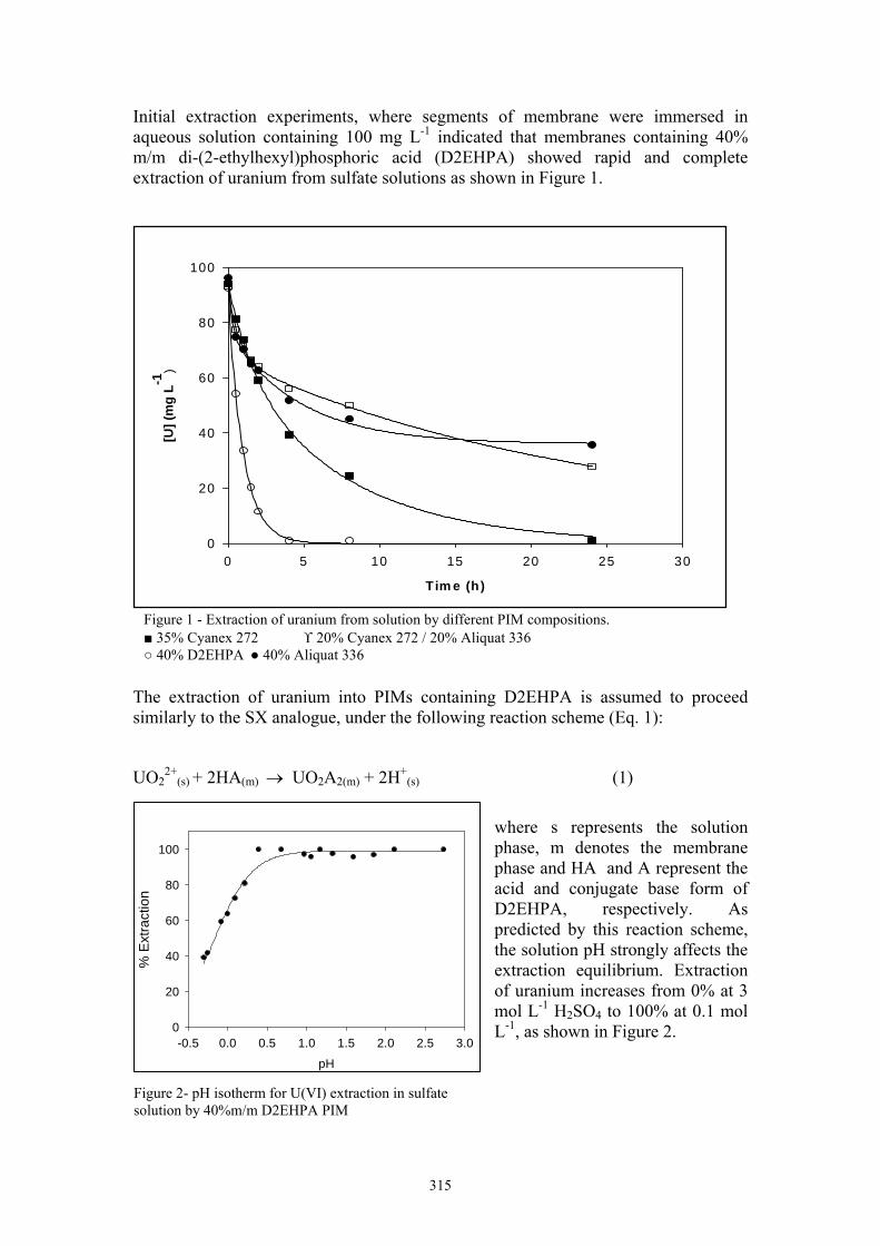
Initial extraction experiments, where segments of membrane were immersed in aqueous solution containing 100 mg L-1 indicated that membranes containing 40% m/m di-(2-ethylhexyl)phosphoric acid (D2EHPA) showed rapid and complete extraction of uranium from sulfate solutions as shown in Figure 1.
The extraction of uranium into PIMs containing D2EHPA is assumed to proceed similarly to the SX analogue, under the following reaction scheme (Eq. 1):
UO22+
(s) + 2HA(m) → UO2A2(m) + 2H+
(s) (1)
where s represents the solution phase, m denotes the membrane phase and HA and A represent the acid and conjugate base form of D2EHPA, respectively. As predicted by this reaction scheme, the solution pH strongly affects the extraction equilibrium. Extraction of uranium increases from 0% at 3 mol L-1 H2SO4 to 100% at 0.1 mol L-1, as shown in Figure 2.
Tim e (h)
0 5 10 15 20 25 30
[U] (
mg
L-1)
0
20
40
60
80
100
Figure 1 - Extraction of uranium from solution by different PIM compositions. 35% Cyanex 272 ϒ 20% Cyanex 272 / 20% Aliquat 336 40% D2EHPA 40% Aliquat 336
pH
-0.5 0.0 0.5 1.0 1.5 2.0 2.5 3.0
% E
xtra
ctio
n
0
20
40
60
80
100
Figure 2- pH isotherm for U(VI) extraction in sulfate solution by 40%m/m D2EHPA PIM
316
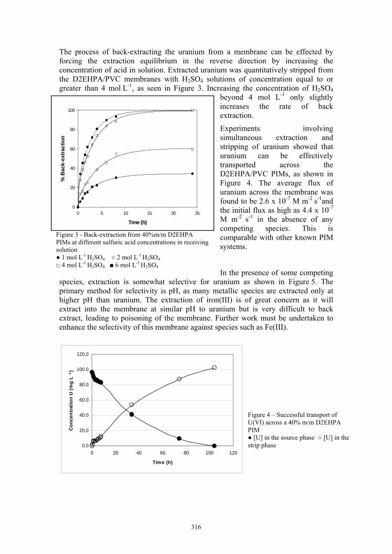
The process of back-extracting the uranium from a membrane can be effected by forcing the extraction equilibrium in the reverse direction by increasing the concentration of acid in solution. Extracted uranium was quantitatively stripped from the D2EHPA/PVC membranes with H2SO4 solutions of concentration equal to or greater than 4 mol L-1, as seen in Figure 3. Increasing the concentration of H2SO4
beyond 4 mol L-1 only slightly increases the rate of back extraction.
Experiments involving simultaneous extraction and stripping of uranium showed that uranium can be effectively transported across the D2EHPA/PVC PIMs, as shown in Figure 4. The average flux of uranium across the membrane was found to be 2.6 x 10⁻⁷ M m-2 s-1and the initial flux as high as 4.4 x 10⁻⁷ M m-2 s-1 in the absence of any competing species. This is comparable with other known PIM systems.
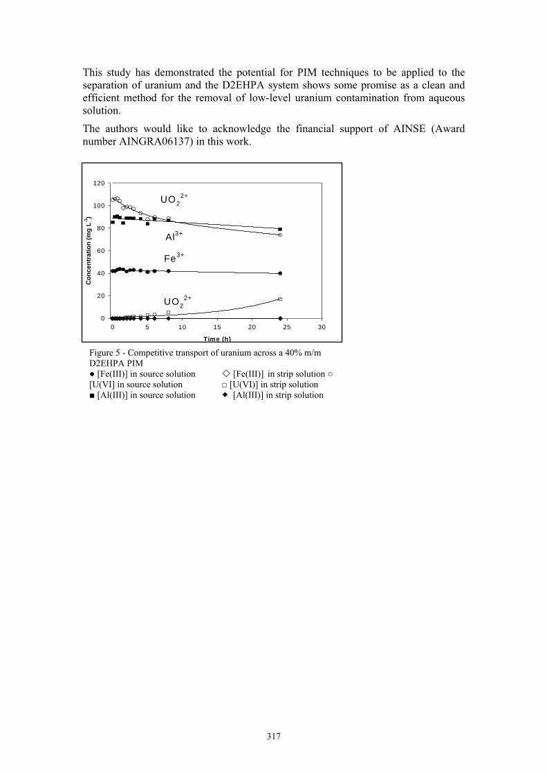
In the presence of some competing species, extraction is somewhat selective for uranium as shown in Figure 5. The primary method for selectivity is pH, as many metallic species are extracted only at higher pH than uranium. The extraction of iron(III) is of great concern as it will extract into the membrane at similar pH to uranium but is very difficult to back extract, leading to poisoning of the membrane. Further work must be undertaken to enhance the selectivity of this membrane against species such as Fe(III).
Time (h)
0 5 10 15 20 25
% B
ack-
extr
actio
n
0
20
40
60
80
100
Figure 3 - Back-extraction from 40%m/m D2EHPA PIMs at different sulfuric acid concentrations in receiving solution 1 mol L-1 H2SO4 2 mol L-1 H2SO4 4 mol L-1 H2SO4 6 mol L-1 H2SO4
0.0
20.0
40.0
60.0
80.0
100.0
120.0
0 20 40 60 80 100 120
Time (h)
Con
cent
ratio
n U
(mg
L-1
)
Figure 4 – Successful transport of U(VI) across a 40% m/m D2EHPA PIM [U] in the source phase [U] in the strip phase
317
This study has demonstrated the potential for PIM techniques to be applied to the separation of uranium and the D2EHPA system shows some promise as a clean and efficient method for the removal of low-level uranium contamination from aqueous solution.
The authors would like to acknowledge the financial support of AINSE (Award number AINGRA06137) in this work.
Time (h)
0 5 10 15 20 25 30
Con
cent
ratio
n (m
g L-1
)
0
20
40
60
80
100
120
UO22+
Al3+
Fe3+
UO22+
Figure 5 - Competitive transport of uranium across a 40% m/m D2EHPA PIM [Fe(III)] in source solution [Fe(III)] in strip solution [U(VI] in source solution [U(VI)] in strip solution [Al(III)] in source solution [Al(III)] in strip solution
318
Ion beam analysis and positive matrix factorisation modeling: tools for exploring aerosol source fingerprints
Eduard Stelcer, David D. Cohen, Michael Prior ANSTO, Institute for Environmental Research, PMB 1, Menai, NSW 2234, Australia
Abstract
ANSTO has been involved in PM2.5 monitoring and analysis since 1991. Long term sampling together with information on concentrations of total collected gravimetric mass, black carbon and 23 elements from hydrogen to lead obtained by accelerator based nuclear analytical methods have been used for generating large data sets. The Positive Matrix Factorisation (PMF) modelling technique has been applied to these data sets for exploring PM2.5 source fingerprints and source contributions at Sydney and Brisbane. Data in this presentation covers sources and their contributions to total PM2.5 pollution at Liverpool (Sydney) from January 1998 to December 2006 and at Rocklea (Brisbane) from January 1998 to December 2003.
Introduction
Fine particle aerosols (PM2.5) with aerodynamic diameter of 2.5µm and less are collected on stretched Teflon filters using cyclone-based samplers [1-2]. Samples are generally collected over a 24-hour period from midnight to midnight every Wednesday and Sunday. Collected samples are analysed by accelerator based Ion Beam Analysis techniques (IBA) using an 8mm-diameter beam of 2.6MeV protons [3-5]. IBA includes four techniques applied simultaneously. PIXE (Particle Induced X-ray Emission) for analysis of the range of elements including Al, Si, P, S, Cl, K, Ca, Ti, V, Cr, Mn, Fe, Co, Cu, Ni, Zn, Br and Pb. PIGE (Particle Induced Gamma-ray Emission) for analysis of F and Na. RBS (Rutherford Back Scattering) for analysis of C, O and N and PESA (Particle Elastic Scattering) for analysis of H. On data obtained by long term sampling and IBA nuclear based analysis the Positive Matrix Factorisation (PMF) statistical receptor-modelling technique [6-10] has been applied to characterise fine aerosol particle origins (fingerprints of sources) and their contributions to the total air pollution at Liverpool (Sydney) and Rocklea (Brisbane). The Liverpool sampling site is located close to the Hume Highway in the centre of the Sydney Basin in a mixed residential and commercial area with an average annual PM2.5 mass concentration of 8±4 µg/m3 during 1998-2006. The Rocklea sampling site is located in an open farm surrounded by light industry and residential areas with extensive heavy vehicle and freight railway components in the traffic and with an average annual PM2.5 mass concentration of 6±3 µg/m3 during 1998-2003.
NOTE: The Australian National Environment Protection Council (NEPC) proposes a new National Environment Protection Measure (NEPM) for PM2.5 particulates to be 8 µg/m3 for the annual average concentration.
Results
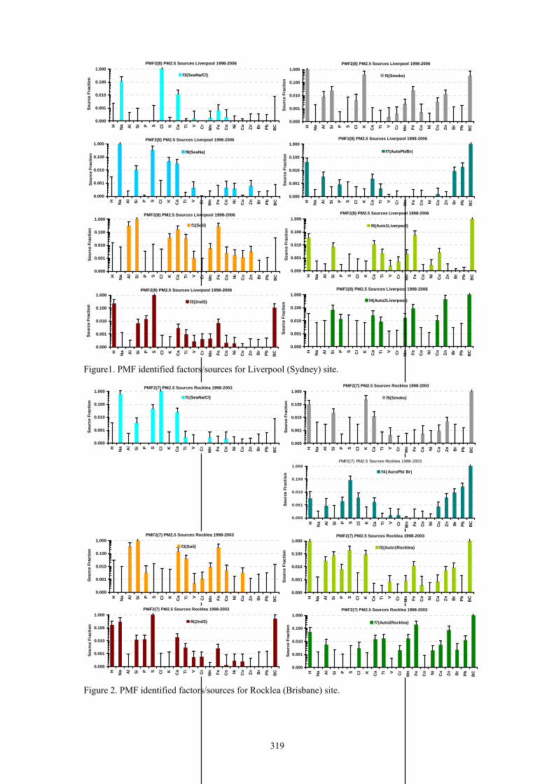
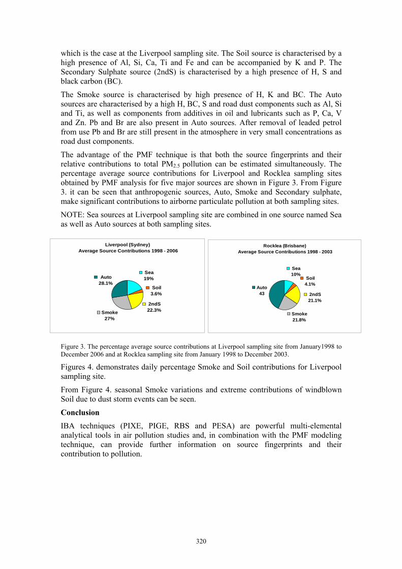
For the Liverpool data 8 factors/sources were identified and are presented in Figure 1. For the Rocklea data 7 factors/sources were identified and are presented in Figure 2. Names of the factors/sources are not defined by the PMF program and are at the discretion of the user. They have been assigned by looking at the major elemental contributors in the elemental mix for each factor/source. For example the Seaspray source is characterised by a high presence of Na and Cl and can be accompanied by elements such as Si, S, K and Ca. It can also appear as chlorine depleted Seaspray
319
Figure1. PMF identified factors/sources for Liverpool (Sydney) site.
Figure 2. PMF identified factors/sources for Rocklea (Brisbane) site.
0.000
0.001
0.010
0.100
1.000
H Na Al Si P S Cl K C
a Ti V Cr
Mn Fe Co Ni
Cu Zn Br
Pb BC
Sour
ce F
ract
ion
f1(Soil)
PMF2(8) PM2.5 Sources Liverpool 1998-2006
0.000
0.001
0.010
0.100
1.000
H Na Al Si P S Cl K C
a Ti V Cr
Mn Fe Co Ni
Cu Zn Br
Pb BC
Sour
ce F
ract
ion
f3(SeaNa/Cl)
PMF2(8) PM2.5 Sources Liverpool 1998-2006
0.000
0.001
0.010
0.100
1.000
H Na Al
Si P S Cl K Ca Ti V Cr
Mn Fe Co Ni
Cu Zn Br
Pb BC
Sour
ce F
ract
ion f4(Auto2Liverpool)
PMF2(8) PM2.5 Sources Liverpool 1998-2006
0.000
0.001
0.010
0.100
1.000
H Na Al
Si P S Cl K Ca Ti V Cr
Mn Fe Co Ni
Cu Zn Br
Pb BC
Sour
ce F
ract
ion
f5(Smoke)
PMF2(8) PM2.5 Sources Liverpool 1998-2006
0.000
0.001
0.010
0.100
1.000
H Na Al
Si P S Cl K Ca Ti V Cr
Mn Fe Co Ni
Cu Zn Br
Pb BC
Sour
ce F
ract
ion
f6(Auto1Liverpool)
PMF2(8) PM2.5 Sources Liverpool 1998-2006
0.000
0.001
0.010
0.100
1.000
H Na Al
Si P S Cl K Ca Ti V Cr
Mn Fe Co Ni
Cu Zn Br
Pb BC
Sour
ce F
ract
ion
f7(AutoPb/Br)
PMF2(8) PM2.5 Sources Liverpool 1998-2006
0.000
0.001
0.010
0.100
1.000
H Na Al
Si P S Cl K C
a Ti V Cr
Mn Fe Co Ni
Cu Zn Br
Pb BC
Sour
ce F
ract
ion f8(SeaNa)
PMF2(8) PM2.5 Sources Liverpool 1998-2006
0.000
0.001
0.010
0.100
1.000
H Na Al Si P S Cl K C
a Ti V Cr
Mn Fe Co Ni
Cu Zn Br
Pb BC
Sour
ce F
ract
ion
f2(2ndS)
PMF2(8) PM2.5 Sources Liverpool 1998-2006
0.000
0.001
0.010
0.100
1.000
H Na Al
Si P S Cl K Ca Ti V Cr
Mn Fe Co Ni
Cu Zn Br
Pb BC
Sour
ce F
ract
ion
f1(SeaNa/Cl)
PMF2(7) PM2.5 Sources Rocklea 1998-2003
0.000
0.001
0.010
0.100
1.000
H Na Al
Si P S Cl K Ca Ti V Cr
Mn Fe Co Ni
Cu Zn Br
Pb BC
Sour
ce F
ract
ion
f3(Soil)
PMF2(7) PM2.5 Sources Rocklea 1998-2003
0.000
0.001
0.010
0.100
1.000
H Na Al
Si P S Cl K C
a Ti V Cr
Mn Fe Co Ni
Cu Zn Br
Pb
BC
Sou
rce
Frac
tion
f4(AutoPb/Br)
PMF2(7) PM2.5 Sources Rocklea 1998-2003
0.000
0.001
0.010
0.100
1.000
H Na Al
Si P S Cl K C
a Ti V Cr
Mn Fe Co Ni
Cu Zn Br
Pb BC
Sour
ce F
ract
ion
f5(Smoke)
PMF2(7) PM2.5 Sources Rocklea 1998-2003
0.000
0.001
0.010
0.100
1.000
H Na Al
Si P S Cl K Ca Ti V Cr
Mn Fe Co Ni
Cu Zn Br
Pb BC
Sour
ce F
ract
ion
f6(2ndS)
PMF2(7) PM2.5 Sources Rocklea 1998-2003
0.000
0.001
0.010
0.100
1.000
H Na Al
Si P S Cl K C
a Ti V Cr
Mn Fe Co Ni
Cu Zn Br
Pb BC
Sour
ce F
ract
ion
f7(Auto2Rocklea)
PMF2(7) PM2.5 Sources Rocklea 1998-2003
0.000
0.001
0.010
0.100
1.000
H Na Al Si P S Cl K Ca Ti V Cr
Mn Fe Co Ni
Cu Zn Br
Pb BC
Sour
ce F
ract
ion
f2(Auto1Rocklea)
PMF2(7) PM2.5 Sources Rocklea 1998-2003
320
Liverpool (Sydney) Average Source Contributions 1998 - 2006
Soil3.6%
2ndS22.3%
Auto28.1%
Sea19%
Smoke27%
which is the case at the Liverpool sampling site. The Soil source is characterised by a high presence of Al, Si, Ca, Ti and Fe and can be accompanied by K and P. The Secondary Sulphate source (2ndS) is characterised by a high presence of H, S and black carbon (BC).
The Smoke source is characterised by high presence of H, K and BC. The Auto sources are characterised by a high H, BC, S and road dust components such as Al, Si and Ti, as well as components from additives in oil and lubricants such as P, Ca, V and Zn. Pb and Br are also present in Auto sources. After removal of leaded petrol from use Pb and Br are still present in the atmosphere in very small concentrations as road dust components.
The advantage of the PMF technique is that both the source fingerprints and their relative contributions to total PM2.5 pollution can be estimated simultaneously. The percentage average source contributions for Liverpool and Rocklea sampling sites obtained by PMF analysis for five major sources are shown in Figure 3. From Figure 3. it can be seen that anthropogenic sources, Auto, Smoke and Secondary sulphate, make significant contributions to airborne particulate pollution at both sampling sites.
NOTE: Sea sources at Liverpool sampling site are combined in one source named Sea as well as Auto sources at both sampling sites.
Figure 3. The percentage average source contributions at Liverpool sampling site from January1998 to December 2006 and at Rocklea sampling site from January 1998 to December 2003.
Figures 4. demonstrates daily percentage Smoke and Soil contributions for Liverpool sampling site.
From Figure 4. seasonal Smoke variations and extreme contributions of windblown Soil due to dust storm events can be seen.
Conclusion
IBA techniques (PIXE, PIGE, RBS and PESA) are powerful multi-elemental analytical tools in air pollution studies and, in combination with the PMF modeling technique, can provide further information on source fingerprints and their contribution to pollution.
Rocklea (Brisbane) Average Source Contributions 1998 - 2003
Smoke21.8%
2ndS21.1%
Soil4.1%
Auto43
Sea10%

321
Figure 4. Daily Percentage Soil and Smoke for Liverpool.
References [1] Malm, W. C., Sisler, J. F., Huffman, D, Eldred, R. A., Cahill, T. A. (1994) Journal of
Geophysical Research. 99, 1347.
[2] Cohen, D. D., Bailey, G. M., Kondepudi, R. (1996) Elemental Analysis by PIXE and other IBA Techniques and their Application to Source Fingerprinting of Atmospheric Fine Particle Pollution, Nucl. Instr. Meth., B109-110, 218-226.
[3] Cohen, D. D., (1999a) Accelerator Based Ion Beam Techniques for Aerosol Analysis. In Elemental Analysis of Airborne Particles. S. Landsberger and M. Creatchman (eds.) Gordon Breach Science Publishers.
[4] David D. Cohen, Ed Stelcer, Olga Hawas, David Garton, IBA Methods for Characterisation of Fine Particulate Atmospheric Pollution: A local, regional and global research problem. Nucl. Instr. and Methods B219-220 (2004) 145-152.
[5] David D. Cohen, David Garton, Eduard Stelcer, Olga Hawas, Accelerator Based Studies of Atmospheric Pollution Processes. Radiation Physics and Chemistry, 71 (2004) 759-767.
[6] Lee E., Chan C. and Paatero P. 1999, Application of positive matrix factorisation in source apportionment of particulate pollutants in Hong Kong, Atmospheric Environment, 33, 3201-3212.
[7] Paatero P. 2004, User’s Guide for Positive Matrix Factorisation Programs PMF and PMF2. YP-Tekniika KY Company.
[8] Andrew Chan, Rod Simpson, David Cohen, Olga Hawas, Eduard Stelser, Lyn Denison, Neil Wong, Gary Golding, Elizabeth Christenson, Willy Gore, Mary Hodge, Eva Comino, Stewart Carswell, Apportionment of Sources of Emission of Particles in Four Major Australian Cities by Positive Matrix Factorisation. Proceedings of 17th International Clean Air Conference, Hobart, Tasmania, Australia, 3-6 May 2005.
[9] B. A. Begum, S.K. Biswas, P. K. Hopke, D.D. Cohen, Multi-elemental analysis and characterisation of atmospheric particulate pollution in Dhaka. Aerosol and Air Quality Research, 6 (2006) 334-359.
[10] David D. Cohen, Eduard Stelcer, Vuong Thu Bac, Quantification of Fine Particle Composition, Sources and Transboundary Transport in Hanoi, Vietnam from 2001-06.14th World Congress, 18th CASANZ Clean Air Conference, Brisbane, QLD, Australia, 9-13 September 2007.
0
20
40
60
80
19
980
70
1
19
981
11
8
19
990
31
4
19
990
80
1
19
991
20
1
20
000
50
3
20
000
91
3
20
010
20
7
20
010
61
3
20
011
01
4
20
020
21
7
20
020
60
9
20
021
11
7
20
030
32
6
20
030
82
7
20
031
22
4
20
040
41
8
20
040
90
1
20
041
22
6
20
050
42
4
20
050
82
4
20
051
22
5
20
060
41
6
20
060
81
3
20
061
21
0
Smoke%
0
20
40Soil%
322
Single ion implantation using nano-apertures: precision placement for CTAP
Jessica A. van Donkelaar 1, Andrew D. Greentree 1, A. Alves 1, C. Yang 1, S. Rubanov 2 and David N. Jamieson 1
1ARC Centre of Excellence for Quantum Computer Technology, 2Bio21 Institute, School of Physics, The University of Melbourne, Parkville, Australia 3010 Email:
There is currently a worldwide effort being applied to the task of building a solid-state quantum computer. Since Kane’s original publication for a silicon based QC device [1] there has been a rise to over 3300 publications per annum on quantum information and devices. Many architectures have been proposed and several are well advanced, meeting the goals of the QC roadmap[2]. These architectures present unprecedented fabrication challenges. In particular, the need for a quantum equivalent to the wire has led to the proposal of a scaleable two-dimensional architecture from Hollenberg et al.[3]. It employs the robust coherent transfer adiabatic passage (CTAP) mechanism that has been demonstrated in optical waveguides [4]. Ion implantation offers the quickest route to demonstrating it in the solid state since it is an established method using existing technologies. However there are problematic issues that warrant further study. Oxygen atoms have around an 8% chance of being recoiled forward into the substrate, introducing contaminants into the device. The impact of ions can cause damage to the necessary surface oxide layer and the substrate though this may actually be beneficial. Issues regarding the precision with which a dopant can be placed are addressed here.
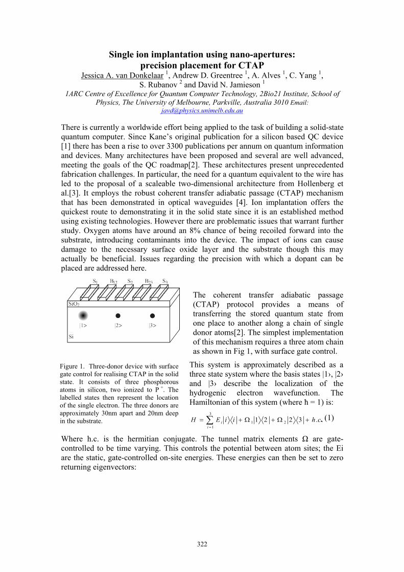
The coherent transfer adiabatic passage (CTAP) protocol provides a means of transferring the stored quantum state from one place to another along a chain of single donor atoms[2]. The simplest implementation of this mechanism requires a three atom chain as shown in Fig 1, with surface gate control.
This system is approximately described as a three state system where the basis states |1›, |2› and |3› describe the localization of the hydrogenic electron wavefunction. The Hamiltonian of this system (where ћ = 1) is:
..3221 21
3
1
chiiEHi
i +Ω+Ω+= ∑=
(1)
Where h.c. is the hermitian conjugate. The tunnel matrix elements Ω are gate-controlled to be time varying. This controls the potential between atom sites; the Ei are the static, gate-controlled on-site energies. These energies can then be set to zero returning eigenvectors:
Figure 1. Three-donor device with surface gate control for realising CTAP in the solid state. It consists of three phosphorous atoms in silicon, two ionized to P +. The labelled states then represent the location of the single electron. The three donors are approximately 30nm apart and 20nm deep in the substrate.

323
( ),
2
321
,31
22
21
222
211
22
21
120
Ω+Ω
Ω+Ω+Ω±Ω=
Ω+Ω
Ω−Ω=
±D
D
(2)
with eigenvalues 22
210 ,0 Ω+Ω±== ±EE (3)
With inspection of (2), the CTAP protocol can be understood as the transition from state |1› to |3›. The system remains in the |D0› state as long as adiabaticity criteria are met, and as the tunnel matrix elements are varied such that Ω2 >> Ω1 at t = tmin to Ω1 >> Ω2 at t = tmax, the electron moves from being localized around the first donor to the third without having been in state |2›. This requires the capability to suppress the tunnel matrix elements to zero and to regulate their increase over time tmax. Adiabaticity must be maintained over the time tmax.
The scale of tmax is limited by the speed of the control electronics and the timescale of decoherence for the quantum state. The adiabaticity criterion is used to relate tmax to the intrinsic tunnel matrix elements Ωmax.
2
0
0
||
||
EE
Dt
HDA
−
⟩∂
∂⟨
=+
+ ( ) 2/32max2
2max1
max2
max1
max )()(2 Ω+ΩΩΩ
=A
t π (4)
where A is the adiabaticity parameter. Within the hydrogenic approximation of Openov[5], Ωmax depends on the inter -donor spacing d.
⎥⎦
⎤⎢⎣
⎡−⎟⎟
⎠
⎞⎜⎜⎝
⎛−⎟⎟
⎠
⎞⎜⎜⎝
⎛=Ω 1exp **
*max
BB ad
adE ( 5)
For phosphorous in silicon we have the scaled Rydberg E*=40 meV and the Bohr radius aB =2.5nm. This theory shows that for a realistic dephasing time limit of ~10 ns, the inter donor spacing (d12=d23), needs to be about 20-30nm. We know address how such a device could be fabricated in practice.
Fabricating such a three atom device can be done with accurate counted atom implantation. Single 14keV phosphorous ions are clearly detected entering a silicon substrate [6] using the existing and tested Colutron system. A beam limiting aperture close to the surface of the substrate will increase precision in ion placement if it masks the surrounding area. Scattering simulations by M. Taylor et al. of MeV He, F and Cu ions through 100nm high aspect ratio apertures suggest that aperture masking is effective[7]. In addition, experimental results of 7.2keV Ar2+ through an aperture 200nm in diameter indicate that charge transfer between the mask and the incident ions is negligible[8]. Circular apertures with diameters as small as 1nm have been demonstrated[9]. Having three apertures in a mask would produce too low a device yield since we cannot tell which of the apertures the detected ion has passed through. Instead we envisage a process of counted atom implantation where one atom passes through an aperture, the aperture is moved a fixed distance from the first site and a second ion is implanted into the substrate through the aperture. This step-and-repeat idea can be extended to have a row of single atoms in the substrate as required. Forming the beam limiting aperture from crossed slots with one patterned by EBL in a PMMA mask on the substrate and the other in a mobile cantilever lessens the precision demanded of the alignment system, in the direction of the slot. Technology
324
is readily available for positioning of the masking aperture to the required accuracy of 20nm.
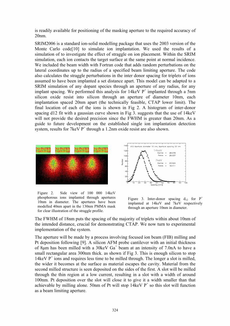
SRIM2006 is a standard ion-solid modelling package that uses the 2003 version of the Monte Carlo code[10] to simulate ion implantation. We used the results of a simulation of to investigate the effect of straggle on ion placement. Within the SRIM simulation, each ion contacts the target surface at the same point at normal incidence. We included the beam width with Fortran code that adds random perturbations on the lateral coordinates up to the radius of a specified beam limiting aperture. The code also calculates the straggle perturbations in the inter donor spacing for triplets of ions assumed to have been implanted a set distance apart. This model can be adapted to a SRIM simulation of any dopant species through an aperture of any radius, for any implant spacing. We performed this analysis for 14keV P+ implanted through a 5nm silicon oxide resist into silicon through an aperture of diameter 10nm, each implantation spaced 20nm apart (the technically feasible, CTAP lower limit). The final location of each of the ions is shown in Fig 2. A histogram of inter-donor spacing d12 fit with a gaussian curve shown in Fig 3. suggests that the use of 14keV will not provide the desired precision since the FWHM is greater than 20nm. As a guide to future development on the established single ion implantation detection system, results for 7keV P+ through a 1.2nm oxide resist are also shown.
The FWHM of 18nm puts the spacing of the majority of triplets within about 10nm of the intended distance, crucial for demonstrating CTAP. We now turn to experimental implementation of the system.
The aperture will be made by a process involving focused ion beam (FIB) milling and Pt deposition following [9]. A silicon AFM probe cantilever with an initial thickness of 8µm has been milled with a 30keV Ga+ beam at an intensity of 7.0nA to have a small rectangular area 300nm thick. as shown if Fig 3. This is enough silicon to stop 14keV P+ ions and requires less time to be milled through. The longer a slot is milled, the wider it becomes at the surface as material escapes the cavity. Material from the second milled structure is seen deposited on the sides of the first. A slot will be milled through the thin region at a low current, resulting in a slot with a width of around 100nm. Pt deposition over the slot will close it to give it a width smaller than that achievable by milling alone. 50nm of Pt will stop 14keV P+ so this slot will function as a beam limiting aperture.
Figure 3. Inter-donor spacing d12 for P+
implanted at 14keV and 7keV respectively through an aperture 10nm in diameter.
Figure 2. Side view of 100 000 14keV phosphorous ions implanted through apertures 10nm in diameter. The apertures have been modelled 40nm apart in the 130nm PMMA mask for clear illustration of the straggle profile.
325
For ions to be successfully implanted and detected the must be able to pass through the aperture with full energy. Current efforts indicate that future work involving IBIC analysis[11] of the aperture will sufficiently characterise a slot.
Within the hydrogenic approximation, this SRIM based analysis of the use of a nano-aperture mask for 20nm ion separation supports the proposed implantation method for the demonstration of CTAP in the solid state. Work has begun towards implementing this precision single ion implantation process in Melbourne.
This work was supported by the Australian Research Council, the Australian Government and by the US National Security Agency (NSA), Advanced Research and Development Activity (ARDA) and the Army Research Office (ARO) under contracts W911NF-04-1-0290.
[1] B. E. Kane, “A silicon-based nuclear spin quantum computer,” Nature (Lond) 393, 133 (1998).
[2] University of California “Quantum Computation Roadmap,” http://qist.lanl.gov/qcomp_map.shtml (2004)
[3] L. C. L. Hollenberg, A. D. Greentree, A. G. Fowler, and C. J. Wellard “Two-dimensional architectures for donor-based quantum computing,” Phys. Rev. B 74, 045311 (2006).
[4] S. Longhi, G. Della Valle, M. Ornigotti, and P. Laporta “Coherent tunneling by adiabatic passage in an optical waveguide system,” E-print: arXiv:0709.3050v1.
[5] L. A. Openov, “Resonant pulse operations on the buried donor charge qubits in semiconductors,” Phys. Rev. B 70, 233313 (2004).
[6] D. N. Jamieson, C. Yang, T. Hopf, S. M. Hearne, C. I. Pakes, S. Prawer, M. Mitic, E. Gauja, S. E. Andresen, F. E. Hudson, A. S. Dzurak, and R. G. Clark “Controlled shallow single-ion implantation in silicon using an active substrate for sub-20-keV ions,” App. Phys. Lett. 86, 202101 (2005).
[7] M.L. Taylor, R.D. Franich, A. Alves, P. Reichart, D.N. Jamieson, and P.N. Johnston “Ion transmission through nano-aperture”' Nucl. Instr. Meth. B 249, 752–755 (2006).
[8] A. Persaud, F. I. Allen “Single ion implantation with scanning probe alignment,” J. Vac. Sci. Tech. B 22(6), 2992-2994 (2004).
[9] T. Schenkel, V. Radmilovic, E. A. Stach, S.J. Park, and A. Persaud “Formation of a few nanometer wide holes in membranes with a dual beam focused ion beam system,” J. Vac. Sci. Technol. B 21Vol.6 (2003).
[10] J. F. Ziegler “SRIM-2003” Nucl. Instr. Meth. B 219–220, 1027–1036 (2004).
[11] C. Yang, D. N Jamieson, S. M. Hearne, C. I. Pakes, B. Rout, E. Gouja, A. J. Dzurak and R. G. Clark “Ion-beam-induced-charge characterisation of particle detectors,” Nucl. Instr. Meth. B 190 212-216 (2002).

326
Template fabricated gold nanotubes membranes: a nucleation and growth study
L. Velleman 1, J.G. Shapter 1 and D. Losic 2
1Flinders University, School of Chemistry, Physics and Earth Sciences, Bedford Park, Adelaide, SA 5042
2 University of South Australia, Ian Wark Research Institute, Mawson Lakes Campus, Mawson Lakes, Adelaide, SA 5095 SUMMARY
Gold nanotube membranes were prepared by electroless deposition of gold within the pores of a polycarbonate (PC) track etched membrane used as a template. Different fabrication parameters such as membrane pore diameter, deposition time and pH of plating solution were studied. Gold nanotubes with a variety of diameters (from < 5nm to > 100nm) have been fabricated and characterised.
Introduction
Development of novel nanoporous materials as specific nanostructured materials with unique surface, structural, and chemical properties is a fast growing research area with enormous potential for applications in various fields such as separation, adsorption, catalysis, sensors, drug delivery, energy storage and fundamental research. Nanotube containing membranes prepared by the template method which consists of ordered arrays of vertically aligned cylindrical channels with sizes of few to tens nm show promise for use as highly selective filters for membrane based chemical and biological separation.1-2 Advantages of gold nanotube membranes are based on properties of the gold (chemical inertness, temperature stability, conductivity), ability to control channel dimensions, ability to use a wide range of surface modifications and functionalisations, flexibility in applying a variety of selectivity approaches (size, sterics, electrostatics, electrophoretic, interfacial, chemical, biorecognition) and capacity to combine separation processes with biosensing.1, 3 The most common approach for fabrication gold nanotube membranes is electroless deposition and the principle is shown in Figure 1. Although the gold
electroless deposition method is a relatively simple and standard method widely used for coating different materials, its application for coating long channels with nano scale dimensions still need to be explored and optimised. The deposition kinetic can be varied through many parameters including the concentration of the plating concentration, pH, temperature, diffusion mechanism inside pores, the pore size, the pore chemistry etc.4 This research aims to study the influence of some of these
Fig. 1. Schematic representation of template fabrication of gold nanotube membranes using electroless gold deposition
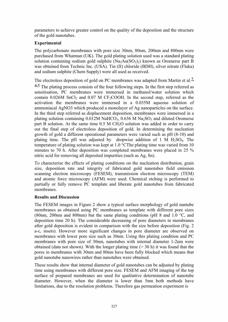
327
parameters to achieve greater control on the quality of the deposition and the structure of the gold nanotubes.
Experimental
The polycarbonate membranes with pore size 30nm, 80nm, 200nm and 800nm were purchased from Whatman (UK). The gold plating solution used was a standard plating solution containing sodium gold sulphite (Na3Au(SO3)2) known as Oromerse part B was obtained from Technic Inc. (USA). Tin (II) chloride (BDH), silver nitrate (Fluka) and sodium sulphite (Chem Supply) were all used as received.
The electroless deposition of gold on PC membranes was adapted from Martin et al.2, 4-5 The plating process consists of the four following steps. In the first step referred as sensitisation, PC membranes were immersed in methanol/water solution which contain 0.026M SnCl2 and 0.07 M CF3COOH. In the second step, referred as the activation the membranes were immersed in a 0.035M aqueous solution of ammoniacal AgNO3 which produced a monolayer of Ag nanoparticles on the surface. In the third step referred as displacement deposition, membranes were immersed in a plating solution containing 0.012M NaHCO3, 0.636 M Na2SO3 and diluted Oromerse part B solution. At the same time 0.5 M CH2O solution was added in order to carry out the final step of electroless deposition of gold. In determining the nucleation growth of gold a different operational parameters were varied such as pH (8-10) and plating time. The pH was adjusted by dropwise addition of 1 M H2SO4. The temperature of plating solution was kept at 1.0 °CThe plating time was varied from 10 minutes to 70 h. After deposition was completed membranes were placed in 25 % nitric acid for removing all deposited impurities (such as Ag, Sn).
To characterise the effects of plating conditions on the nucleation distribution, grain size, deposition rate and integrity of fabricated gold nanotubes field emission scanning electron microscopy (FESEM), transmission electron microscopy (TEM) and atomic force microscopy (AFM) were used. Chemical etching is performed to partially or fully remove PC template and liberate gold nanotubes from fabricated membranes.
Results and Discussion
The FESEM images in Figure 2 show a typical surface morphology of gold nantube membranes as obtained using PC membranes as template with different pore sizes (80nm, 200nm and 800nm) but the same plating conditions (pH 8 and 1.0 °C, and deposition time 20 h). The considerable decreasing of pore diameters in membranes after gold deposition is evident in comparison with the size before deposition (Fig. 2 a-c, insets). However more significant changes in pore diameter are observed on membranes with lower pore size such as 30nm. Using this plating condition and PC membranes with pore size of 30nm, nanotubes with internal diameter 1-2nm were obtained (data not shown). With the longer plating time (> 30 h) it was found that the pores in membranes with 30nm and 80nm have been fully blocked which means that gold nanotube nanowires rather than nanotubes were obtained.
These results show that internal diameter of gold nanotubes can be adjusted by plating time using membranes with different pore size. FESEM and AFM imaging of the top surface of prepared membranes are used for qualitative determination of nanotube diameter. However, when the diameter is lower than 5nm both methods have limitations, due to the resolution problems. Therefore gas permeation experiment is
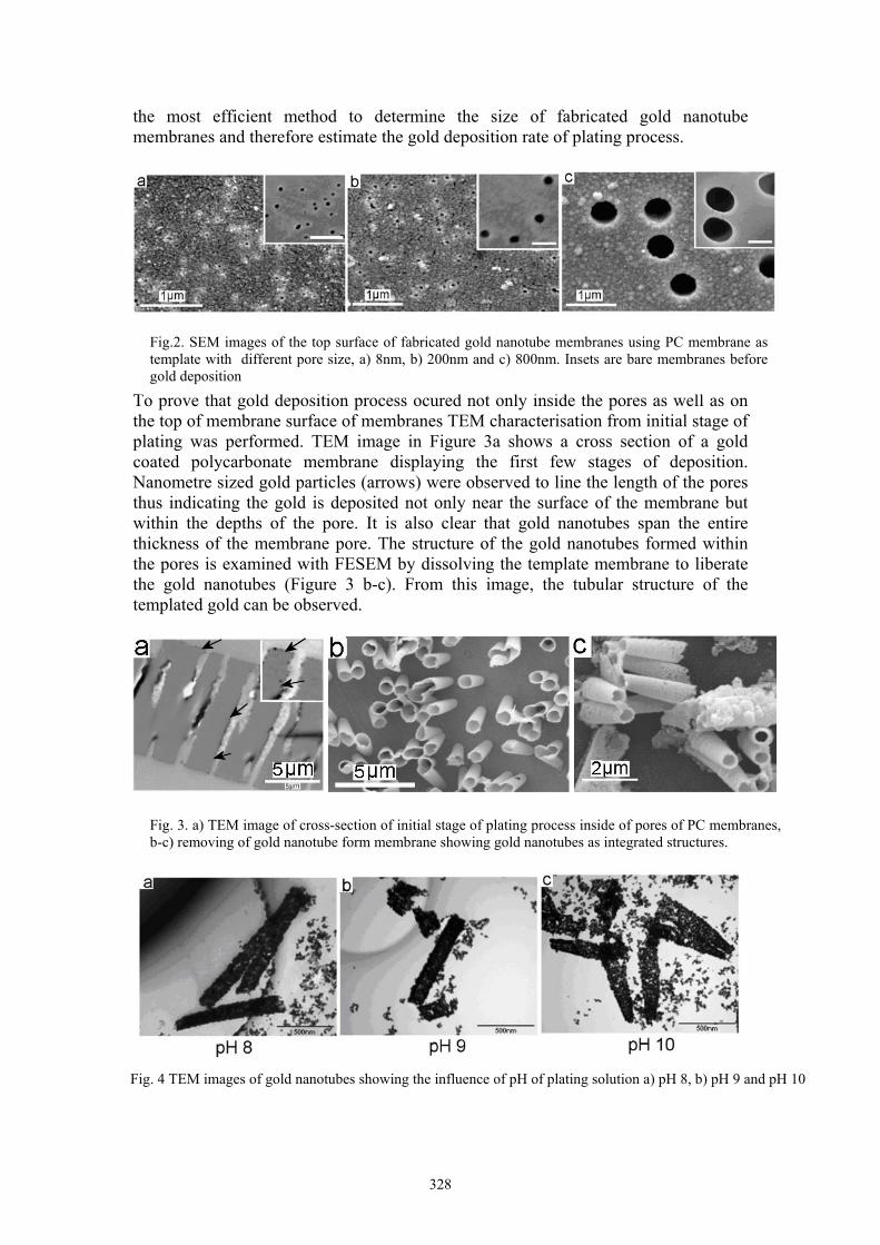
328
the most efficient method to determine the size of fabricated gold nanotube membranes and therefore estimate the gold deposition rate of plating process.
To prove that gold deposition process ocured not only inside the pores as well as on the top of membrane surface of membranes TEM characterisation from initial stage of plating was performed. TEM image in Figure 3a shows a cross section of a gold coated polycarbonate membrane displaying the first few stages of deposition. Nanometre sized gold particles (arrows) were observed to line the length of the pores thus indicating the gold is deposited not only near the surface of the membrane but within the depths of the pore. It is also clear that gold nanotubes span the entire thickness of the membrane pore. The structure of the gold nanotubes formed within the pores is examined with FESEM by dissolving the template membrane to liberate the gold nanotubes (Figure 3 b-c). From this image, the tubular structure of the templated gold can be observed.
Fig.2. SEM images of the top surface of fabricated gold nanotube membranes using PC membrane as template with different pore size, a) 8nm, b) 200nm and c) 800nm. Insets are bare membranes before gold deposition
Fig. 3. a) TEM image of cross-section of initial stage of plating process inside of pores of PC membranes, b-c) removing of gold nanotube form membrane showing gold nanotubes as integrated structures.
Fig. 4 TEM images of gold nanotubes showing the influence of pH of plating solution a) pH 8, b) pH 9 and pH 10
329
As mentioned previously, the deposition kinetics and characteristics can vary depending on the parameters used for the plating bath. Nanometer sized gold particles are deposited on the pore walls and as plating time continues these particles form a compact gold layer. The size of these gold particles and their nucleation distance is dependent on several factors, the concentration of gold, pH and temperature of the plating bath. To characterise the growth of gold nanotubes inside using different plating conditions such as pH and plating time TEM imaging is performed. Figure 4 a-c chows TEM images of gold nanotubes formed using different pH (8-10) of plating solution. As pH is increased (Figure 5, from a) to c)) the nanotubes become shorter and less dense, implying that the nucleation distance increases and the nanotubes become more brittle. As pH is increased,
the deposition rate increases, thus attributing to the inhomogeneous structure of the gold nanotube. The optimal pH of 8 provides a slower deposition rate and a more homogenous nanotube is formed Figure 5 a.
Conclusions
Gold nanotube membranes have been formed using the template based electroless deposition method. The kinetics of the electroless deposition method was studied in order to attain a better understanding of the film growth kinetics. In this invesitgation, factors such as plating time and pH of plating bath were varied to explore the optimal parameters for quality electroless depositon. These gold nanotube membranes hold promise for the development of highly selective membranes for molecular separations.
Acknowledgment:
The authors thank the Australian Research Council (ARC), the University of South Australia and Flinders University for financial support.
References: 1 Kohli, P.; Martin, C.R. J. Drug Deliv. Sci. Tech., 2005, 15, 49-57.
2 Jirage, K.B.; Hulteen, J.C.; Martin, C.R. Science, 1997, 278, 655-658.
3 Wirtz, M.; Parker, M.; Kobayashi, Y.; Martin, C.R. A European Journal, 2002, 16, 3572-3578.
4 Menon, V.P., and Martin, C.R., Anal. Chem., 1995. 67, 1920- 1928.
5 Wirtz, M.; Martin, C.R. Adv. Mat., 2003, 15, 455-458.
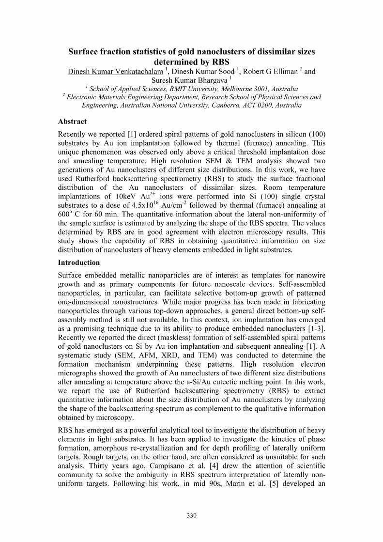
330
Surface fraction statistics of gold nanoclusters of dissimilar sizes determined by RBS
Dinesh Kumar Venkatachalam 1, Dinesh Kumar Sood 1, Robert G Elliman 2 and Suresh Kumar Bhargava 1
1 School of Applied Sciences, RMIT University, Melbourne 3001, Australia 2 Electronic Materials Engineering Department, Research School of Physical Sciences and
Engineering, Australian National University, Canberra, ACT 0200, Australia
Abstract
Recently we reported [1] ordered spiral patterns of gold nanoclusters in silicon (100) substrates by Au ion implantation followed by thermal (furnace) annealing. This unique phenomenon was observed only above a critical threshold implantation dose and annealing temperature. High resolution SEM & TEM analysis showed two generations of Au nanoclusters of different size distributions. In this work, we have used Rutherford backscattering spectrometry (RBS) to study the surface fractional distribution of the Au nanoclusters of dissimilar sizes. Room temperature implantations of 10keV Au2+ ions were performed into Si (100) single crystal substrates to a dose of 4.5x10¹⁶ Au/cm-2 followed by thermal (furnace) annealing at 600o C for 60 min. The quantitative information about the lateral non-uniformity of the sample surface is estimated by analyzing the shape of the RBS spectra. The values determined by RBS are in good agreement with electron microscopy results. This study shows the capability of RBS in obtaining quantitative information on size distribution of nanoclusters of heavy elements embedded in light substrates.
Introduction
Surface embedded metallic nanoparticles are of interest as templates for nanowire growth and as primary components for future nanoscale devices. Self-assembled nanoparticles, in particular, can facilitate selective bottom-up growth of patterned one-dimensional nanostructures. While major progress has been made in fabricating nanoparticles through various top-down approaches, a general direct bottom-up self-assembly method is still not available. In this context, ion implantation has emerged as a promising technique due to its ability to produce embedded nanoclusters [1-3]. Recently we reported the direct (maskless) formation of self-assembled spiral patterns of gold nanoclusters on Si by Au ion implantation and subsequent annealing [1]. A systematic study (SEM, AFM, XRD, and TEM) was conducted to determine the formation mechanism underpinning these patterns. High resolution electron micrographs showed the growth of Au nanoclusters of two different size distributions after annealing at temperature above the a-Si/Au eutectic melting point. In this work, we report the use of Rutherford backscattering spectrometry (RBS) to extract quantitative information about the size distribution of Au nanoclusters by analyzing the shape of the backscattering spectrum as complement to the qualitative information obtained by microscopy.
RBS has emerged as a powerful analytical tool to investigate the distribution of heavy elements in light substrates. It has been applied to investigate the kinetics of phase formation, amorphous re-crystallization and for depth profiling of laterally uniform targets. Rough targets, on the other hand, are often considered as unsuitable for such analysis. Thirty years ago, Campisano et al. [4] drew the attention of scientific community to solve the ambiguity in RBS spectrum interpretation of laterally non-uniform targets. Following his work, in mid 90s, Marin et al. [5] developed an
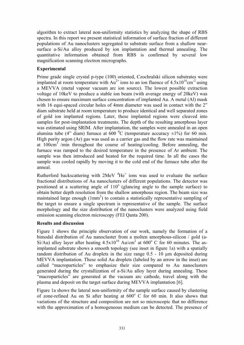
331
algorithm to extract lateral non-uniformity statistics by analyzing the shape of RBS spectra. In this report we present statistical information of surface fraction of different populations of Au nanoclusters segregated to substrate surface from a shallow near-surface a-Si/Au alloy produced by ion implantation and thermal annealing. The quantitative information obtained from RBS is confirmed by several low magnification scanning electron micrographs.
Experimental
Prime grade single crystal p-type (100) oriented, Czochralski silicon substrates were implanted at room temperature with Au2+ ions to an ion fluence of 4.5x1016cm-2 using a MEVVA (metal vapour vacuum arc ion source). The lowest possible extraction voltage of 10keV to produce a stable ion beam (with average energy of 20keV) was chosen to ensure maximum surface concentration of implanted Au. A metal (Al) mask with 16 equi-spaced circular holes of 4mm diameter was used in contact with the 2” diam substrate held at room temperature to produce identical and well separated zones of gold ion implanted regions. Later, these implanted regions were cleaved into samples for post-implantation treatments. The depth of the resulting amorphous layer was estimated using SRIM. After implantation, the samples were annealed in an open alumina tube (4” diam) furnace at 600 0C (temperature accuracy ±1%) for 60 min. High purity argon (Ar) gas was used as a carrier gas and the flow rate was maintained at 100cm3 /min throughout the course of heating/cooling. Before annealing, the furnace was ramped to the desired temperature in the presence of Ar ambient. The sample was then introduced and heated for the required time. In all the cases the sample was cooled rapidly by moving it to the cold end of the furnace tube after the anneal.
Rutherford backscattering with 2MeV 4He+ ions was used to evaluate the surface fractional distributions of Au nanoclusters of different populations. The detector was positioned at a scattering angle of 110o (glancing angle to the sample surface) to obtain better depth resolution from the shallow amorphous region. The beam size was maintained large enough (1mm2) to contain a statistically representative sampling of the target to ensure a single spectrum is representative of the sample. The surface morphology and the size distribution of the nanoclusters were analyzed using field emission scanning electron microscopy (FEI Qanta 200).
Results and discussion
Figure 1 shows the principle observation of our work, namely the formation of a bimodal distribution of Au nanocluster from a molten amorphous-silicon / gold (a-Si/Au) alloy layer after heating 4.5x10¹⁶ Au/cm2 at 600o C for 60 minutes. The as-implanted substrate shows a smooth topology (see inset in figure 1a) with a spatially random distribution of Au droplets in the size range 0.5 - 10 µm deposited during MEVVA implantation. These solid Au droplets (labeled by an arrow in the inset) are called “macroparticles” to emphasize their size compared to Au nanoclusters generated during the crystallization of a-Si/Au alloy layer during annealing. These “macroparticles” are generated at the vacuum arc cathode, travel along with the plasma and deposit on the target surface during MEVVA implantation [6].
Figure 1a shows the lateral non-uniformity of the sample surface caused by clustering of zone-refined Au on Si after heating at 600o C for 60 min. It also shows that variations of the structure and composition are not so microscopic that no difference with the approximation of a homogeneous medium can be detected. The presence of
332
two generations of Au nanoclusters of different sizes is shown in figure 1b. The bigger clusters are of the size range 400-500nm whereas the second generation clusters range between 50-75nm. The size of the Au nanoclusters has been determined from several low magnification scanning electron micrographs. The increase in width of the size distribution is similar to ‘Ostwald ripening’ process where the bigger clusters grow at the expense of smaller ones at higher annealing temperatures.
Figure 1: SEM micrographs showing surface morphology of 4.5x10¹⁶ Au/cm2 implanted into Si (100) and annealed at 600o C for 60 min a) low magnification image showing de-wetting of Au on Si (Inset showing as-implanted substrate); and b) high magnification image showing bimodal distribution of Au nanoclusters.
Figure 2 shows the corresponding backscattering spectra obtained with 2MeV He+ ions. The spectrum obtained from the as-implanted (un-annealed) sample shows a well defined Gaussian distribution of a 30nm near-surface a-Si/Au alloy layer. The small tail of Au profile in the as-implanted sample is due to the random size and spatial distribution of the Au “macroparticles”. After annealing at 600o C for 60 min the implanted Au condensed into Au islands, leaving free a large potion of underlying silicon substrate. This is evidenced by a strong decrease in the Au yield and a gradual decrease in the intensity towards lower energies.
The Au profile after annealing at 600oC in figure 2 confirms the presence of two generation of Au nanoclusters of different size distributions. The long Au tail is due to the lateral non-uniformity of the substrate surface and the size distribution of the larger Au nanoclusters. (Similar effects were observed by Campisano et al. [4] in a laterally non-uniform lead (Pb) thin film on Si.) In contrast, the smaller clusters lead to resolution limited surface peak [7].
By analyzing the shape of the Au profile before and after annealing, it is estimated that after heating at 600oC, Au nanoclusters of the size range 400-500nm account for 70% of the Au coverage, whilst the smaller nanoclusters account for the remainder. To strengthen this estimation, the samples were annealed at temperatures above and below 600oC for very short annealing cycles (5-30s) to study the early stages of Au nanocluster formation. The early stages of Au de-wetting and Au nanocluster formation is estimated by comparing the RBS spectra recorded after different annealing conditions (results will be reported elsewhere).
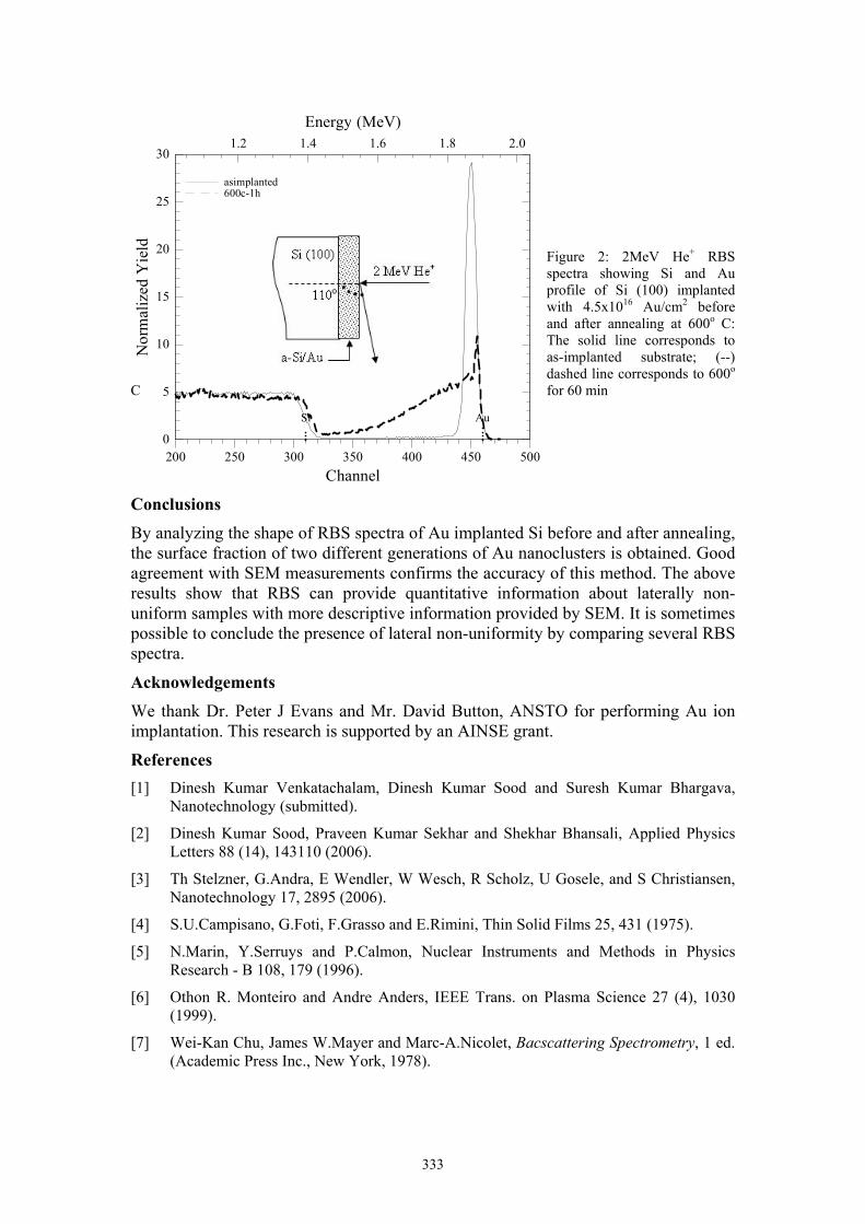
333
200 250 300 350 400 450 500Channel
0
5
10
15
20
25
30N
orm
aliz
edY
ield
1.2 1.4 1.6 1.8 2.0Energy (MeV)
asimplanted600c-1h
AuSi
Figure 2: 2MeV He+ RBS spectra showing Si and Au profile of Si (100) implanted with 4.5x10¹⁶ Au/cm2 before and after annealing at 600o C: The solid line corresponds to as-implanted substrate; (--) dashed line corresponds to 600o
C for 60 min
Conclusions
By analyzing the shape of RBS spectra of Au implanted Si before and after annealing, the surface fraction of two different generations of Au nanoclusters is obtained. Good agreement with SEM measurements confirms the accuracy of this method. The above results show that RBS can provide quantitative information about laterally non-uniform samples with more descriptive information provided by SEM. It is sometimes possible to conclude the presence of lateral non-uniformity by comparing several RBS spectra.
Acknowledgements
We thank Dr. Peter J Evans and Mr. David Button, ANSTO for performing Au ion implantation. This research is supported by an AINSE grant.
References [1] Dinesh Kumar Venkatachalam, Dinesh Kumar Sood and Suresh Kumar Bhargava,
Nanotechnology (submitted).
[2] Dinesh Kumar Sood, Praveen Kumar Sekhar and Shekhar Bhansali, Applied Physics Letters 88 (14), 143110 (2006).
[3] Th Stelzner, G.Andra, E Wendler, W Wesch, R Scholz, U Gosele, and S Christiansen, Nanotechnology 17, 2895 (2006).
[4] S.U.Campisano, G.Foti, F.Grasso and E.Rimini, Thin Solid Films 25, 431 (1975).
[5] N.Marin, Y.Serruys and P.Calmon, Nuclear Instruments and Methods in Physics Research - B 108, 179 (1996).
[6] Othon R. Monteiro and Andre Anders, IEEE Trans. on Plasma Science 27 (4), 1030 (1999).
[7] Wei-Kan Chu, James W.Mayer and Marc-A.Nicolet, Bacscattering Spectrometry, 1 ed. (Academic Press Inc., New York, 1978).
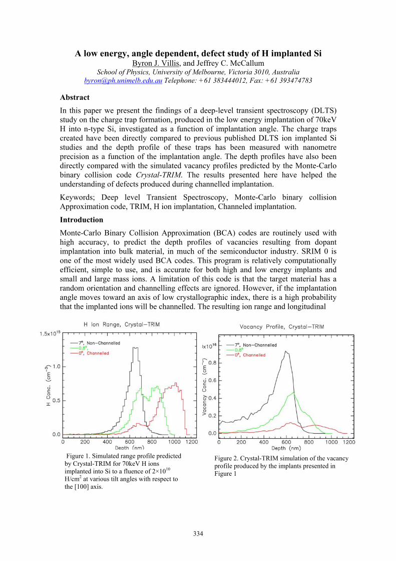
334
A low energy, angle dependent, defect study of H implanted Si Byron J. Villis, and Jeffrey C. McCallum
School of Physics, University of Melbourne, Victoria 3010, Australia [email protected] Telephone: +61 383444012, Fax: +61 393474783
Abstract
In this paper we present the findings of a deep-level transient spectroscopy (DLTS) study on the charge trap formation, produced in the low energy implantation of 70keV H into n-type Si, investigated as a function of implantation angle. The charge traps created have been directly compared to previous published DLTS ion implanted Si studies and the depth profile of these traps has been measured with nanometre precision as a function of the implantation angle. The depth profiles have also been directly compared with the simulated vacancy profiles predicted by the Monte-Carlo binary collision code Crystal-TRIM. The results presented here have helped the understanding of defects produced during channelled implantation.
Keywords; Deep level Transient Spectroscopy, Monte-Carlo binary collision Approximation code, TRIM, H ion implantation, Channeled implantation.
Introduction
Monte-Carlo Binary Collision Approximation (BCA) codes are routinely used with high accuracy, to predict the depth profiles of vacancies resulting from dopant implantation into bulk material, in much of the semiconductor industry. SRIM 0 is one of the most widely used BCA codes. This program is relatively computationally efficient, simple to use, and is accurate for both high and low energy implants and small and large mass ions. A limitation of this code is that the target material has a random orientation and channelling effects are ignored. However, if the implantation angle moves toward an axis of low crystallographic index, there is a high probability that the implanted ions will be channelled. The resulting ion range and longitudinal
Figure 2. Crystal-TRIM simulation of the vacancy profile produced by the implants presented in Figure 1
Figure 1. Simulated range profile predicted by Crystal-TRIM for 70keV H ions implanted into Si to a fluence of 2×10¹⁰
H/cm2 at various tilt angles with respect to the [100] axis.
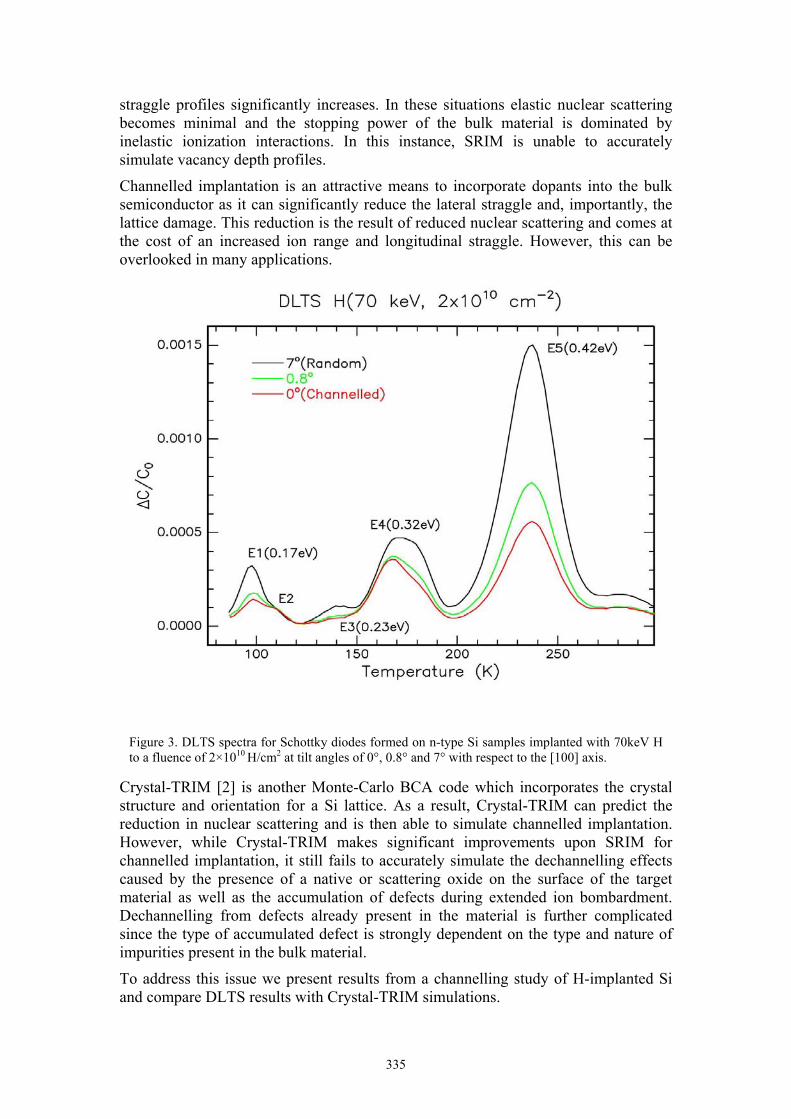
335
straggle profiles significantly increases. In these situations elastic nuclear scattering becomes minimal and the stopping power of the bulk material is dominated by inelastic ionization interactions. In this instance, SRIM is unable to accurately simulate vacancy depth profiles.
Channelled implantation is an attractive means to incorporate dopants into the bulk semiconductor as it can significantly reduce the lateral straggle and, importantly, the lattice damage. This reduction is the result of reduced nuclear scattering and comes at the cost of an increased ion range and longitudinal straggle. However, this can be overlooked in many applications.
Crystal-TRIM [2] is another Monte-Carlo BCA code which incorporates the crystal structure and orientation for a Si lattice. As a result, Crystal-TRIM can predict the reduction in nuclear scattering and is then able to simulate channelled implantation. However, while Crystal-TRIM makes significant improvements upon SRIM for channelled implantation, it still fails to accurately simulate the dechannelling effects caused by the presence of a native or scattering oxide on the surface of the target material as well as the accumulation of defects during extended ion bombardment. Dechannelling from defects already present in the material is further complicated since the type of accumulated defect is strongly dependent on the type and nature of impurities present in the bulk material.
To address this issue we present results from a channelling study of H-implanted Si and compare DLTS results with Crystal-TRIM simulations.
Figure 3. DLTS spectra for Schottky diodes formed on n-type Si samples implanted with 70keV H to a fluence of 2×10¹⁰ H/cm2 at tilt angles of 0°, 0.8° and 7° with respect to the [100] axis.
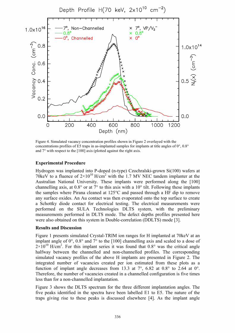
336
Experimental Procedure
Hydrogen was implanted into P-doped (n-type) Czochralski-grown Si(100) wafers at 70keV to a fluence of 2×10¹⁰ H/cm2 with the 1.7 MV NEC tandem implanter at the Australian National University. These implants were performed along the [100] channelling axis, at 0.8° or at 7° to this axis with a 10° tilt. Following these implants the samples where Pirana cleaned at 125°C and passed through a HF dip to remove any surface oxides. An Au contact was then evaporated onto the top surface to create a Schottky diode contact for electrical testing. The electrical measurements were performed on the SULA Technologies DLTS system, with the preliminary measurements performed in DLTS mode. The defect depths profiles presented here were also obtained on this system in Double-correlation (DDLTS) mode [3].
Results and Discussion
Figure 1 presents simulated Crystal-TRIM ion ranges for H implanted at 70keV at an implant angle of 0°, 0.8° and 7° to the [100] channelling axis and scaled to a dose of 2×10¹⁰ H/cm2. For this implant series it was found that 0.8° was the critical angle halfway between the channelled and non-channelled profiles. The corresponding simulated vacancy profiles of the above H implants are presented in Figure 2. The integrated number of vacancies created per ion estimated from these plots as a function of implant angle decreases from 13.3 at 7°, 6.82 at 0.8° to 2.64 at 0°. Therefore, the number of vacancies created in a channelled configuration is five times less than for a non-channelled implantation.
Figure 3 shows the DLTS spectrum for the three different implantation angles. The five peaks identified in the spectra have been labelled E1 to E5. The nature of the traps giving rise to these peaks is discussed elsewhere [4]. As the implant angle
Figure 4. Simulated vacancy concentration profiles shown in Figure 2 overlayed with the concentrations profiles of E5 traps in as-implanted samples for implants at title angles of 0°, 0.8° and 7° with respect to the [100] axis (plotted against the right axis.
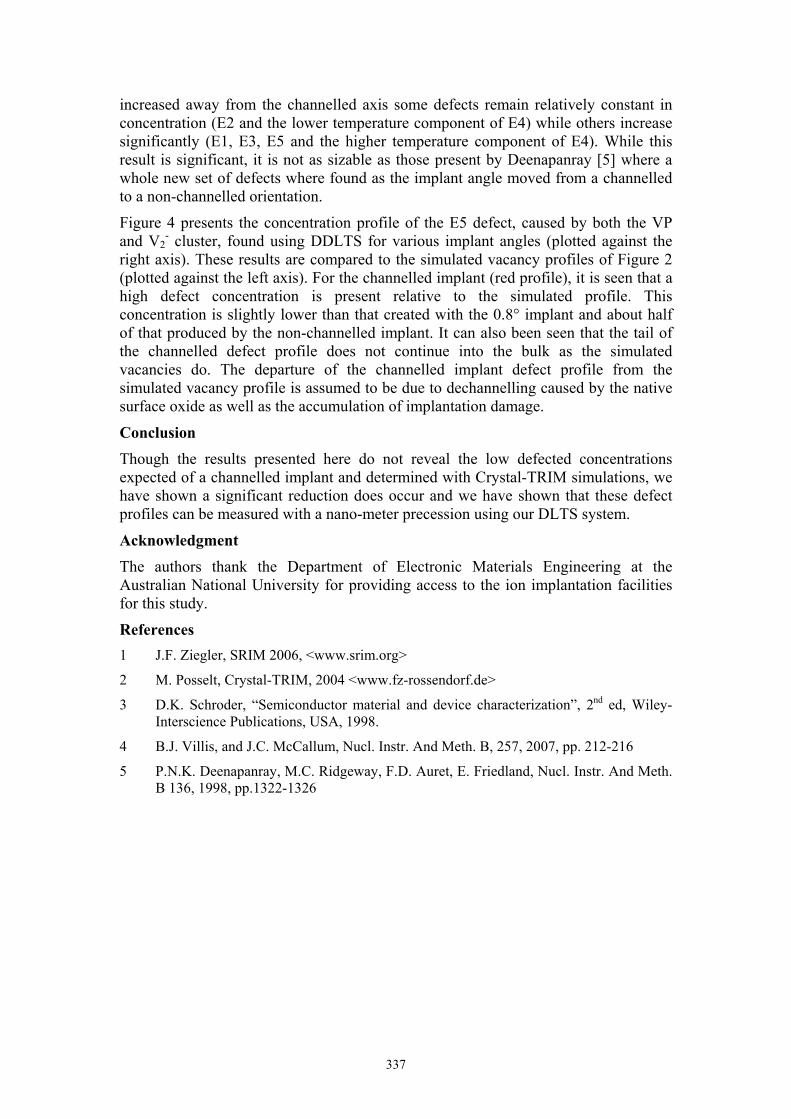
337
increased away from the channelled axis some defects remain relatively constant in concentration (E2 and the lower temperature component of E4) while others increase significantly (E1, E3, E5 and the higher temperature component of E4). While this result is significant, it is not as sizable as those present by Deenapanray [5] where a whole new set of defects where found as the implant angle moved from a channelled to a non-channelled orientation.
Figure 4 presents the concentration profile of the E5 defect, caused by both the VP and V2
- cluster, found using DDLTS for various implant angles (plotted against the right axis). These results are compared to the simulated vacancy profiles of Figure 2 (plotted against the left axis). For the channelled implant (red profile), it is seen that a high defect concentration is present relative to the simulated profile. This concentration is slightly lower than that created with the 0.8° implant and about half of that produced by the non-channelled implant. It can also been seen that the tail of the channelled defect profile does not continue into the bulk as the simulated vacancies do. The departure of the channelled implant defect profile from the simulated vacancy profile is assumed to be due to dechannelling caused by the native surface oxide as well as the accumulation of implantation damage.
Conclusion
Though the results presented here do not reveal the low defected concentrations expected of a channelled implant and determined with Crystal-TRIM simulations, we have shown a significant reduction does occur and we have shown that these defect profiles can be measured with a nano-meter precession using our DLTS system.
Acknowledgment
The authors thank the Department of Electronic Materials Engineering at the Australian National University for providing access to the ion implantation facilities for this study.
References 1 J.F. Ziegler, SRIM 2006, <www.srim.org>
2 M. Posselt, Crystal-TRIM, 2004 <www.fz-rossendorf.de>
3 D.K. Schroder, “Semiconductor material and device characterization”, 2nd ed, Wiley-Interscience Publications, USA, 1998.
4 B.J. Villis, and J.C. McCallum, Nucl. Instr. And Meth. B, 257, 2007, pp. 212-216
5 P.N.K. Deenapanray, M.C. Ridgeway, F.D. Auret, E. Friedland, Nucl. Instr. And Meth. B 136, 1998, pp.1322-1326
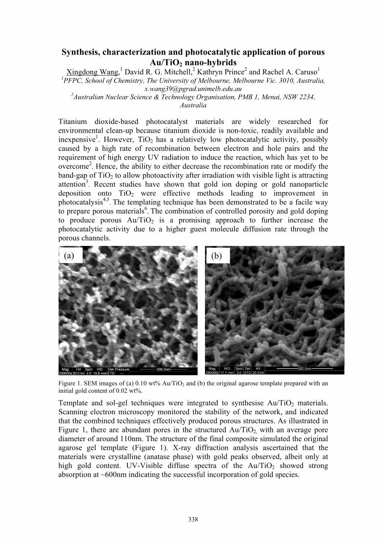
338
Synthesis, characterization and photocatalytic application of porous Au/TiO2 nano-hybrids
Xingdong Wang,1 David R. G. Mitchell,2 Kathryn Prince2 and Rachel A. Caruso1 1PFPC, School of Chemistry, The University of Melbourne, Melbourne Vic. 3010, Australia,
[email protected] 2Australian Nuclear Science & Technology Organisation, PMB 1, Menai, NSW 2234,
Australia
Titanium dioxide-based photocatalyst materials are widely researched for environmental clean-up because titanium dioxide is non-toxic, readily available and inexpensive1. However, TiO2 has a relatively low photocatalytic activity, possibly caused by a high rate of recombination between electron and hole pairs and the requirement of high energy UV radiation to induce the reaction, which has yet to be overcome2. Hence, the ability to either decrease the recombination rate or modify the band-gap of TiO2 to allow photoactivity after irradiation with visible light is attracting attention3. Recent studies have shown that gold ion doping or gold nanoparticle deposition onto TiO2 were effective methods leading to improvement in photocatalysis4,5. The templating technique has been demonstrated to be a facile way to prepare porous materials6. The combination of controlled porosity and gold doping to produce porous Au/TiO2 is a promising approach to further increase the photocatalytic activity due to a higher guest molecule diffusion rate through the porous channels.
Figure 1. SEM images of (a) 0.10 wt% Au/TiO2 and (b) the original agarose template prepared with an initial gold content of 0.02 wt%.
Template and sol-gel techniques were integrated to synthesise Au/TiO2 materials. Scanning electron microscopy monitored the stability of the network, and indicated that the combined techniques effectively produced porous structures. As illustrated in Figure 1, there are abundant pores in the structured Au/TiO2, with an average pore diameter of around 110nm. The structure of the final composite simulated the original agarose gel template (Figure 1). X-ray diffraction analysis ascertained that the materials were crystalline (anatase phase) with gold peaks observed, albeit only at high gold content. UV-Visible diffuse spectra of the Au/TiO2 showed strong absorption at ~600nm indicating the successful incorporation of gold species.
(a) (b)
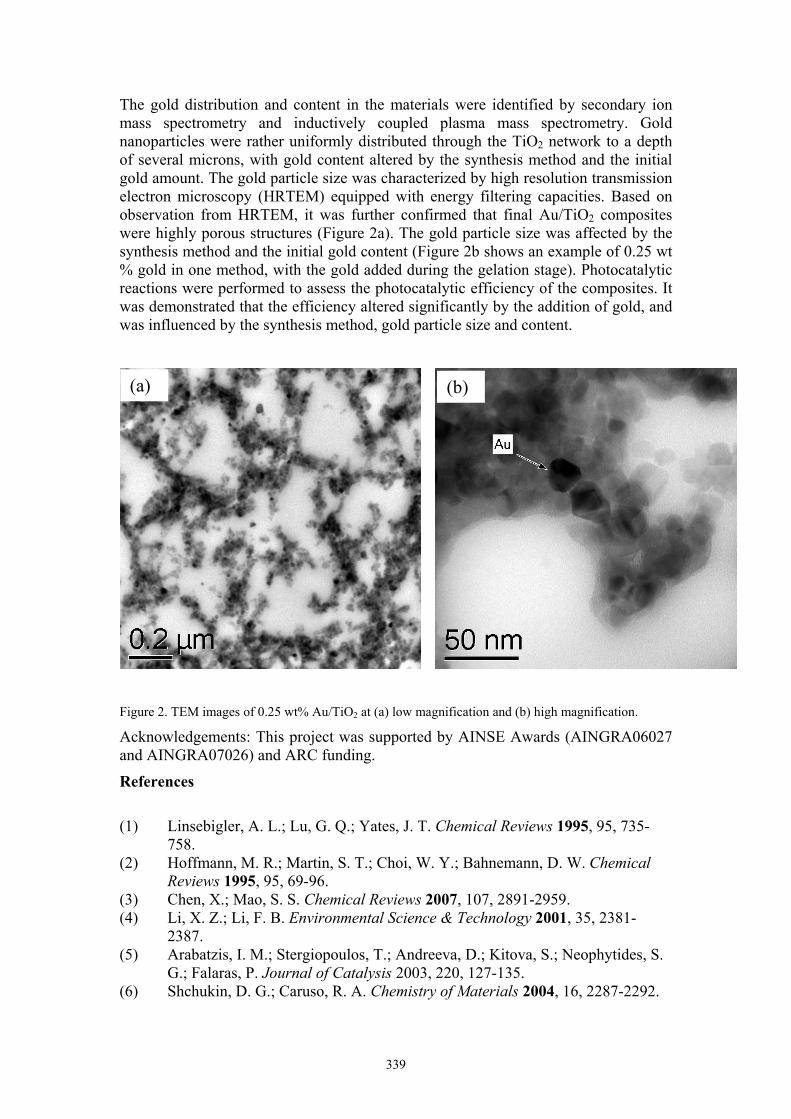
339
The gold distribution and content in the materials were identified by secondary ion mass spectrometry and inductively coupled plasma mass spectrometry. Gold nanoparticles were rather uniformly distributed through the TiO2 network to a depth of several microns, with gold content altered by the synthesis method and the initial gold amount. The gold particle size was characterized by high resolution transmission electron microscopy (HRTEM) equipped with energy filtering capacities. Based on observation from HRTEM, it was further confirmed that final Au/TiO2 composites were highly porous structures (Figure 2a). The gold particle size was affected by the synthesis method and the initial gold content (Figure 2b shows an example of 0.25 wt % gold in one method, with the gold added during the gelation stage). Photocatalytic reactions were performed to assess the photocatalytic efficiency of the composites. It was demonstrated that the efficiency altered significantly by the addition of gold, and was influenced by the synthesis method, gold particle size and content.
Figure 2. TEM images of 0.25 wt% Au/TiO2 at (a) low magnification and (b) high magnification.
Acknowledgements: This project was supported by AINSE Awards (AINGRA06027 and AINGRA07026) and ARC funding.
References
(1) Linsebigler, A. L.; Lu, G. Q.; Yates, J. T. Chemical Reviews 1995, 95, 735-
758. (2) Hoffmann, M. R.; Martin, S. T.; Choi, W. Y.; Bahnemann, D. W. Chemical
Reviews 1995, 95, 69-96. (3) Chen, X.; Mao, S. S. Chemical Reviews 2007, 107, 2891-2959. (4) Li, X. Z.; Li, F. B. Environmental Science & Technology 2001, 35, 2381-
2387. (5) Arabatzis, I. M.; Stergiopoulos, T.; Andreeva, D.; Kitova, S.; Neophytides, S.
G.; Falaras, P. Journal of Catalysis 2003, 220, 127-135. (6) Shchukin, D. G.; Caruso, R. A. Chemistry of Materials 2004, 16, 2287-2292.
(a) (b)
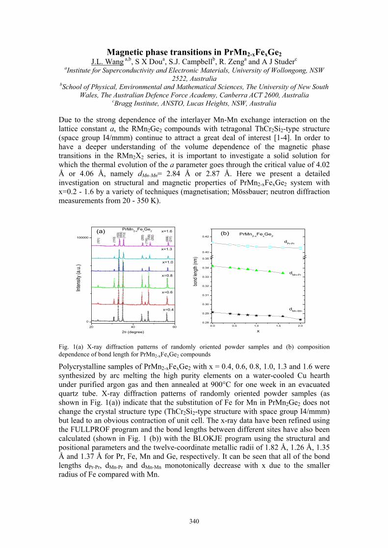
340
Magnetic phase transitions in PrMn2-xFexGe2 J.L. Wang a,b, S X Doua, S.J. Campbellb, R. Zenga and A J Studerc
aInstitute for Superconductivity and Electronic Materials, University of Wollongong, NSW 2522, Australia
bSchool of Physical, Environmental and Mathematical Sciences, The University of New South Wales, The Australian Defence Force Academy, Canberra ACT 2600, Australia
cBragg Institute, ANSTO, Lucas Heights, NSW, Australia
Due to the strong dependence of the interlayer Mn-Mn exchange interaction on the lattice constant a, the RMn2Ge2 compounds with tetragonal ThCr2Si2-type structure (space group I4/mmm) continue to attract a great deal of interest [1-4]. In order to have a deeper understanding of the volume dependence of the magnetic phase transitions in the RMn2X2 series, it is important to investigate a solid solution for which the thermal evolution of the a parameter goes through the critical value of 4.02 Å or 4.06 Å, namely dMn-Mn= 2.84 Å or 2.87 Å. Here we present a detailed investigation on structural and magnetic properties of PrMn2-xFexGe2 system with x=0.2 - 1.6 by a variety of techniques (magnetisation; Mössbauer; neutron diffraction measurements from 20 - 350 K).
Fig. 1(a) X-ray diffraction patterns of randomly oriented powder samples and (b) composition dependence of bond length for PrMn2-xFexGe2 compounds
Polycrystalline samples of PrMn2-xFexGe2 with x = 0.4, 0.6, 0.8, 1.0, 1.3 and 1.6 were synthesized by arc melting the high purity elements on a water-cooled Cu hearth under purified argon gas and then annealed at 900°C for one week in an evacuated quartz tube. X-ray diffraction patterns of randomly oriented powder samples (as shown in Fig. 1(a)) indicate that the substitution of Fe for Mn in PrMn2Ge2 does not change the crystal structure type (ThCr2Si2-type structure with space group I4/mmm) but lead to an obvious contraction of unit cell. The x-ray data have been refined using the FULLPROF program and the bond lengths between different sites have also been calculated (shown in Fig. 1 (b)) with the BLOKJE program using the structural and positional parameters and the twelve-coordinate metallic radii of 1.82 Å, 1.26 Å, 1.35 Å and 1.37 Å for Pr, Fe, Mn and Ge, respectively. It can be seen that all of the bond lengths dPr-Pr, dMn-Pr and dMn-Mn monotonically decrease with x due to the smaller radius of Fe compared with Mn.
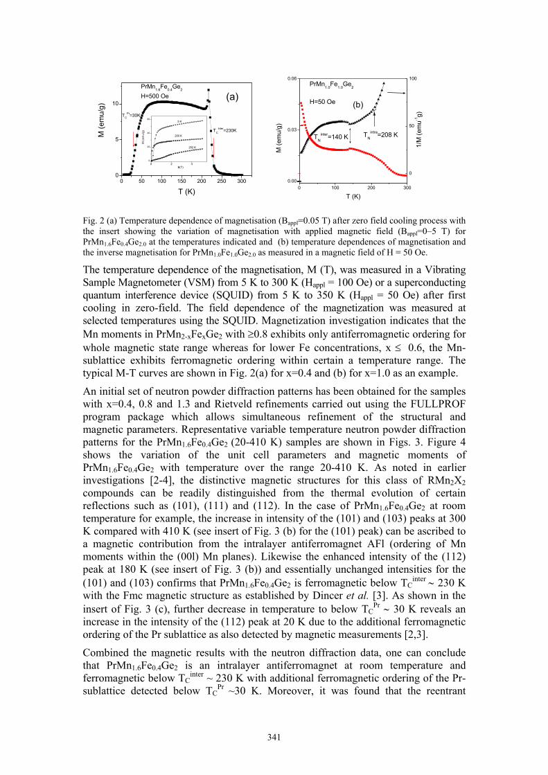
341
Fig. 2 (a) Temperature dependence of magnetisation (Bappl=0.05 T) after zero field cooling process with the insert showing the variation of magnetisation with applied magnetic field (Bappl=0–5 T) for PrMn1.6Fe0.4Ge2.0 at the temperatures indicated and (b) temperature dependences of magnetisation and the inverse magnetisation for PrMn1.0Fe1.0Ge2.0 as measured in a magnetic field of H = 50 Oe.
The temperature dependence of the magnetisation, M (T), was measured in a Vibrating Sample Magnetometer (VSM) from 5 K to 300 K (Happl = 100 Oe) or a superconducting quantum interference device (SQUID) from 5 K to 350 K (Happl = 50 Oe) after first cooling in zero-field. The field dependence of the magnetization was measured at selected temperatures using the SQUID. Magnetization investigation indicates that the Mn moments in PrMn2-xFexGe2 with ≥0.8 exhibits only antiferromagnetic ordering for whole magnetic state range whereas for lower Fe concentrations, x ≤ 0.6, the Mn-sublattice exhibits ferromagnetic ordering within certain a temperature range. The typical M-T curves are shown in Fig. 2(a) for x=0.4 and (b) for x=1.0 as an example.
An initial set of neutron powder diffraction patterns has been obtained for the samples with x=0.4, 0.8 and 1.3 and Rietveld refinements carried out using the FULLPROF program package which allows simultaneous refinement of the structural and magnetic parameters. Representative variable temperature neutron powder diffraction patterns for the PrMn1.6Fe0.4Ge2 (20-410 K) samples are shown in Figs. 3. Figure 4 shows the variation of the unit cell parameters and magnetic moments of PrMn1.6Fe0.4Ge2 with temperature over the range 20-410 K. As noted in earlier investigations [2-4], the distinctive magnetic structures for this class of RMn2X2 compounds can be readily distinguished from the thermal evolution of certain reflections such as (101), (111) and (112). In the case of PrMn1.6Fe0.4Ge2 at room temperature for example, the increase in intensity of the (101) and (103) peaks at 300 K compared with 410 K (see insert of Fig. 3 (b) for the (101) peak) can be ascribed to a magnetic contribution from the intralayer antiferromagnet AFl (ordering of Mn moments within the (00l) Mn planes). Likewise the enhanced intensity of the (112) peak at 180 K (see insert of Fig. 3 (b)) and essentially unchanged intensities for the (101) and (103) confirms that PrMn1.6Fe0.4Ge2 is ferromagnetic below TC
inter ∼ 230 K with the Fmc magnetic structure as established by Dincer et al. [3]. As shown in the insert of Fig. 3 (c), further decrease in temperature to below TC
Pr ∼ 30 K reveals an increase in the intensity of the (112) peak at 20 K due to the additional ferromagnetic ordering of the Pr sublattice as also detected by magnetic measurements [2,3].
Combined the magnetic results with the neutron diffraction data, one can conclude that PrMn1.6Fe0.4Ge2 is an intralayer antiferromagnet at room temperature and ferromagnetic below TC
inter ~ 230 K with additional ferromagnetic ordering of the Pr-sublattice detected below TC
Pr ~30 K. Moreover, it was found that the reentrant
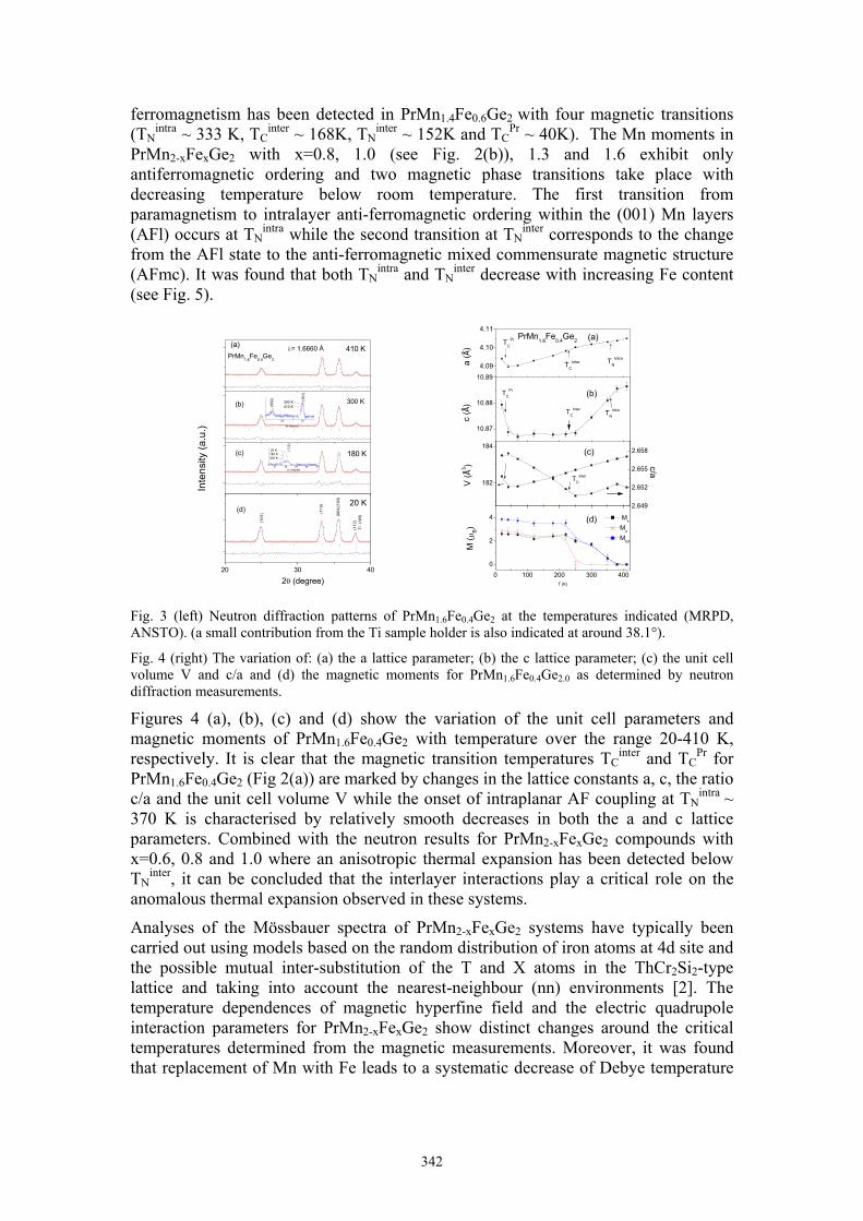
342
ferromagnetism has been detected in PrMn1.4Fe0.6Ge2 with four magnetic transitions (TN
intra ~ 333 K, TCinter ~ 168K, TN
inter ~ 152K and TCPr ~ 40K). The Mn moments in
PrMn2-xFexGe2 with x=0.8, 1.0 (see Fig. 2(b)), 1.3 and 1.6 exhibit only antiferromagnetic ordering and two magnetic phase transitions take place with decreasing temperature below room temperature. The first transition from paramagnetism to intralayer anti-ferromagnetic ordering within the (001) Mn layers (AFl) occurs at TN
intra while the second transition at TNinter corresponds to the change
from the AFl state to the anti-ferromagnetic mixed commensurate magnetic structure (AFmc). It was found that both TN
intra and TNinter decrease with increasing Fe content
(see Fig. 5).
Fig. 3 (left) Neutron diffraction patterns of PrMn1.6Fe0.4Ge2 at the temperatures indicated (MRPD, ANSTO). (a small contribution from the Ti sample holder is also indicated at around 38.1°).
Fig. 4 (right) The variation of: (a) the a lattice parameter; (b) the c lattice parameter; (c) the unit cell volume V and c/a and (d) the magnetic moments for PrMn1.6Fe0.4Ge2.0 as determined by neutron diffraction measurements.
Figures 4 (a), (b), (c) and (d) show the variation of the unit cell parameters and magnetic moments of PrMn1.6Fe0.4Ge2 with temperature over the range 20-410 K, respectively. It is clear that the magnetic transition temperatures TC
inter and TCPr for
PrMn1.6Fe0.4Ge2 (Fig 2(a)) are marked by changes in the lattice constants a, c, the ratio c/a and the unit cell volume V while the onset of intraplanar AF coupling at TN
intra ~ 370 K is characterised by relatively smooth decreases in both the a and c lattice parameters. Combined with the neutron results for PrMn2-xFexGe2 compounds with x=0.6, 0.8 and 1.0 where an anisotropic thermal expansion has been detected below TN
inter, it can be concluded that the interlayer interactions play a critical role on the anomalous thermal expansion observed in these systems.
Analyses of the Mössbauer spectra of PrMn2-xFexGe2 systems have typically been carried out using models based on the random distribution of iron atoms at 4d site and the possible mutual inter-substitution of the T and X atoms in the ThCr2Si2-type lattice and taking into account the nearest-neighbour (nn) environments [2]. The temperature dependences of magnetic hyperfine field and the electric quadrupole interaction parameters for PrMn2-xFexGe2 show distinct changes around the critical temperatures determined from the magnetic measurements. Moreover, it was found that replacement of Mn with Fe leads to a systematic decrease of Debye temperature
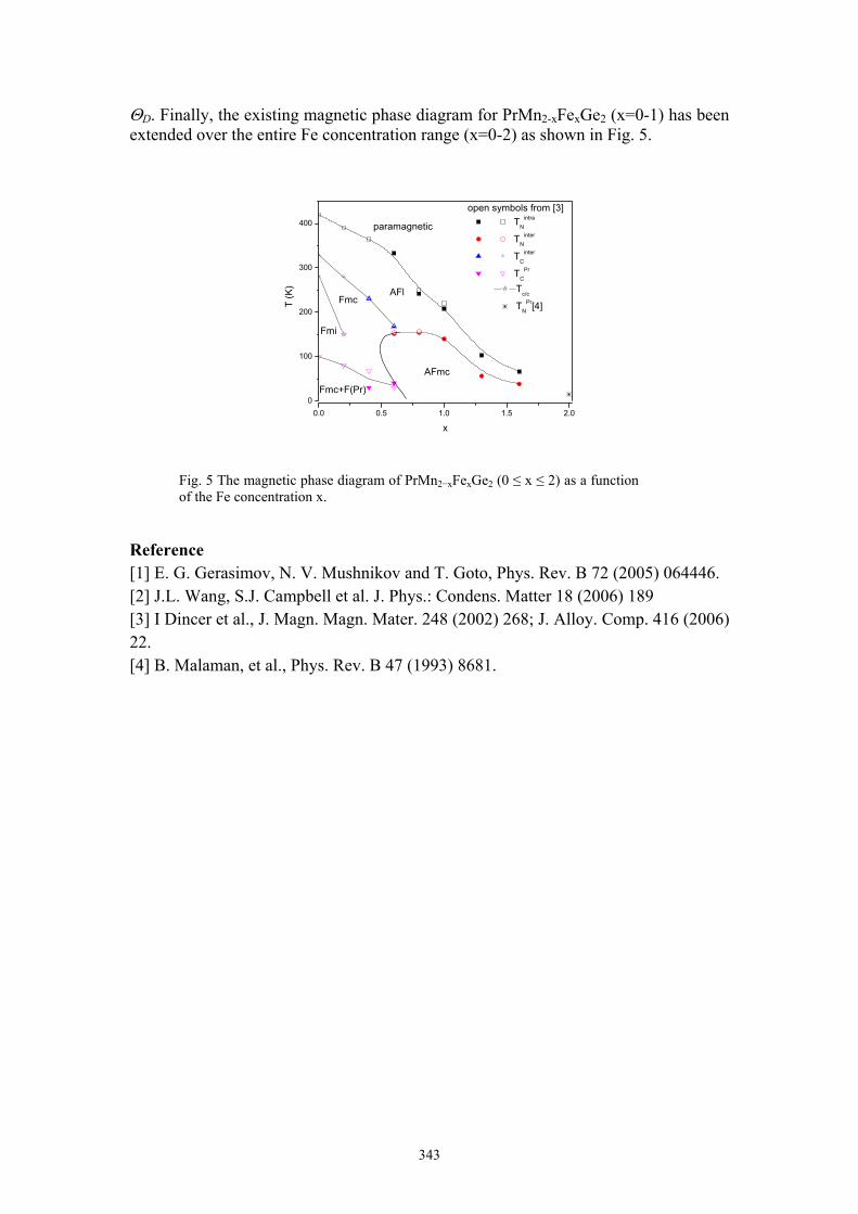
343
ΘD. Finally, the existing magnetic phase diagram for PrMn2-xFexGe2 (x=0-1) has been extended over the entire Fe concentration range (x=0-2) as shown in Fig. 5.
Reference [1] E. G. Gerasimov, N. V. Mushnikov and T. Goto, Phys. Rev. B 72 (2005) 064446. [2] J.L. Wang, S.J. Campbell et al. J. Phys.: Condens. Matter 18 (2006) 189 [3] I Dincer et al., J. Magn. Magn. Mater. 248 (2002) 268; J. Alloy. Comp. 416 (2006) 22. [4] B. Malaman, et al., Phys. Rev. B 47 (1993) 8681.
Fig. 5 The magnetic phase diagram of PrMn2−xFexGe2 (0 ≤ x ≤ 2) as a function of the Fe concentration x.

344
History of natural environmental events in a pristine estuary: ostracod proxies and 210Pb chronology from Wingan Inlet, Victoria
Mark Thomas Warne School of Life and Environmental Sciences, Deakin University (Melbourne Campus), 221
Burwood Hwy, Burwood, 3125, Vic. [email protected]
Introduction
Wingan Inlet is a near pristine estuary located within Croajinglong National Park in East Gippsland, Victoria. The upper estuary occurs in a drowned river valley incised into granitic rocks. The lower estuary is a shallow lagoon partly enclosed by a sand barrier breached by a small outlet that remains open to the sea. The estuary is surrounded by native vegetation including rainforest, coastal scrub, marshes and intertidal mud and sand flats. Sediment cores extracted from the estuary have revealed shifts in estuarine sedimentary environments / facies through time. These shifts are evidenced in cores by variations in fossilised ostracod assemblages and / or changes in lithology.
Cores
Three sediment cores ranging from 1.2 metres to 0.3 metres in length were collected using 50mm and 100mm diameter Livingston corers during February, 2006 from mid to upper estuary settings within Wingan Inlet (Wingan 2, Wingan 3 and Wingan 5). The Wingan 2 core was a 1 metre long (50mm diameter) core taken in approximately 0.5 metres water depth at a very low tide. The core was from a mid estuary mudflat setting approximately 400 metres north of the Wingan Inlet jetty and approximately 40 metres from the western shore of the estuary. The Wingan 3 core was a 32cm long (50mm diameter) core from a position immediately adjacent to the Wingan 2 core. The reason for taking the Wingan 3 core was because of suspected collection related sediment disturbance at the top of the Wingan 2 core. Both Wingan 2 and 3 cores were of mud with scattered shells and shell fragments. The Wingan 5 core was a 1.2 metre long (100mm diameter) Livingston core taken in approximately 4 metres water depth at a very low tide. The core was taken from an upper estuary distributary channel setting approximately 1 km north of the Wingan Inlet jetty and approximately 70 metres from the western shore of the inlet. The Wingan 5 core ranged from a poorly sorted, shelly and muddy gravel near the base, to a poorly sorted sandy mud devoid of shelly material near the top of the core.
Two suites of samples were taken from the cores. The first was used for 210Pb dating and the second for micropalaeontological analyses of subfossil ostracod faunas. A total of 31 samples (0.5 – 1cm slices) from the three cores were processed for 210Pb dating. A total of 13 samples (3cm slices) from these three cores were processed as part of the micropalaeontological analyses. From the 13 micropalaeontological samples approximately 4,000 microscopic ostracod specimens were extracted.
Lead 210 Profiles
Thirty-one samples from Wingan Inlet sediment cores 2, 3 & 5 were subject to standard Pb210 dating procedures at the Australian Nuclear Science and Technology Organisation (ANSTO). Of these thirty-one samples analysed, twenty-four samples generated results useful for dating core materials. Eleven representative ages from these twenty-four dated samples are indicated on the core diagrams below. Pb210
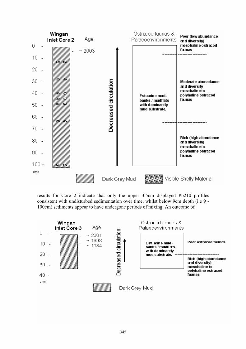
345
results for Core 2 indicate that only the upper 3.5cm displayed Pb210 profiles consistent with undisturbed sedimentation over time, whilst below 9cm depth (i.e 9 -100cm) sediments appear to have undergone periods of mixing. An outcome of
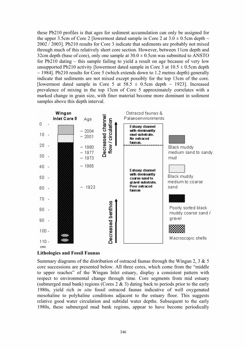
346
these Pb210 profiles is that ages for sediment accumulation can only be assigned for the upper 3.5cm of Core 2 [lowermost dated sample in Core 2 at 3.0 ± 0.5cm depth ~ 2002 / 2003]. Pb210 results for Core 3 indicate that sediments are probably not mixed through much of this relatively short core section. However, between 11cm depth and 32cm depth (base of core), only one sample at 30.0 ± 0.5cm was submitted to ANSTO for Pb210 dating – this sample failing to yield a result on age because of very low unsupported Pb210 activity [lowermost dated sample in Core 3 at 10.5 ± 0.5cm depth ~ 1984]. Pb210 results for Core 5 (which extends down to 1.2 metres depth) generally indicate that sediments are not mixed except possibly for the top 13cm of the core. [lowermost dated sample in Core 5 at 58.5 ± 0.5cm depth ~ 1923]. Increased prevalence of mixing in the top 13cm of Core 5 approximately correlates with a marked change in grain size, with finer material become more dominant in sediment samples above this depth interval.
Lithologies and Fossil Faunas
Summary diagrams of the distribution of ostracod faunas through the Wingan 2, 3 & 5 core successions are presented below. All three cores, which come from the “middle to upper reaches” of the Wingan Inlet estuary, display a consistent pattern with respect to environmental change through time. Core segments from mid estuary (submerged mud bank) regions (Cores 2 & 3) dating back to periods prior to the early 1980s, yield rich in situ fossil ostracod faunas indicative of well oxygenated mesohaline to polyhaline conditions adjacent to the estuary floor. This suggests relative good water circulation and subtidal water depths. Subsequent to the early 1980s, these submerged mud bank regions, appear to have become periodically
347
exposed “mudflat” regions, and generally contain low abundance / low diversity ostracod faunas (or no ostracod faunas).
In distributary channel regions (Core 5), ostracod faunas are rare because of the increased flow conditions, but there is evidence for overall decreased water velocity (flow) conditions from the sedimentary successions (up-sequence decrease in grain size) subsequent to the early 1980s. This may be due to evulsion or decreased river discharge.
Conclusions
Given that Wingan Inlet is a strongly tidal estuary that is permanently open to the sea; it is possible that evidence for decreased water circulation between the early 1980s and 2006 within the middle to upper reaches of the estuary relates to a diminished frequency of high river discharge events and consequent decreased frequency of sediment “flushing” from the estuary. This perhaps relates to decreased precipitation (rainfall) within the region over the last few decades up to 2006, and thus may relate to the effects of local climate variability or broader scale climate change. The effects of the 2007 East Gippsland floods on the Wingan Inlet estuarine system were not assessed in this study. However, this study has demonstrated that climate variability or change probably has an impact on the distribution and extent of different estuarine sediment substrates and benthic habitats.
348
Iron deposition in archaeological teeth A-M. M. Williams a and R. Siegeleb
a School of Medical Sciences, private bag 24, University of Tasmania, Hobart, 7001, Australia
b Australian Nuclear Science and Technology Organisation, PMB 1, Menai NSW, 2234, Australia.
Introduction
Trace element levels in tooth enamel have been used as indicators of the diet and environmental exposure of a person. This makes it possible to use archaeological teeth to investigate diet and environmental exposure in past populations. However, this requires that no post mortem alteration has taken place in the tooth enamel for the element of interest or that it is possible to remove the contamination to reveal a ‘clean’ signal.
This paper uses trace element surface analysis and trace element profiles to address the question of post mortem alteration (diagenesis) of iron (Fe) in tooth enamel.
Although bone has long been known to be subject to post mortem change 1-3, teeth, especially tooth enamel is considered to be more stable and therefore less likely to alter post mortem 4,5. If tooth enamel is in fact resistant to post mortem alteration, then teeth may have value in determining the diet and health of past populations. The focus of this paper, Fe, is an important dietary trace element. Iron is widespread in the environment but in general it is poorly absorbed by the body. Deficiency leads to anaemia, impaired immune function and may delay growth6. It is thought that Fe deposits in the enamel at the time of tooth formation with very little change once the enamel is fully formed 7. Therefore iron levels in tooth enamel may have potential to determine iron exposure during childhood. Iron is distributed in enamel with a possible slight degree of enrichment on the outer surface of the tooth 8. Iron concentrations on surface enamel of modern teeth are generally in the range of 3-130 ppm 9,10 . However, Solis et al measured iron in modern teeth at levels up to 700 ppm 11.
As previously mentioned a problem with trace element analysis in archaeological teeth is the possible post mortem alteration (diagenesis) of trace elements in teeth12. Previous researchers found that Pb profiles in tooth enamel show similar distributions in archaeological and modern teeth suggesting that they are not affected by diagenesis 13,14. The exception to this was seen when remains were in contact with very high Pb levels such as a lead coffin or very high levels of lead in the soil 15,16. Although Fe has not been extensively studied in relation to diagenesis, results have shown higher levels of Fe in archaeological teeth than modern teeth which may indicate that Fe accumulates in teeth post mortem 17-19.
For this paper Fe levels in a large sample of archaeological and modern teeth were measured using ion beam surface analysis techniques and the distribution of iron within the enamel of a small number of teeth was investigated using microprobe mapping techniques.
Materials and Methods
The archaeological teeth investigated in this study came from children 3 to 12 years old, who died between 1863 and 1891 at the Randwick Destitute Children’s Asylum, Sydney, Australia. The children came from a background of poverty and sometimes
349
of neglect and ill health. Historical records and anthropological analysis of the remains indicate they were short for their age and suffered, at some stage, from chronic severe illnesses and/or malnutrition 20. During 1995-96 the remains of 65 children were excavated from an unmarked cemetery . The soil at the cemetery was sandy, the pH varied from 3.03 to 5.62 and the exchangeable cation content was extremely low 21. Iron levels in the grave soil ranged from 140ppm to 4400 ppm with an average of 700 ppm21. The modern teeth (n = 22) used for comparison were removed from children living in Sydney, who were undergoing orthodontic treatment. Teeth were caries free and in good condition. The archaeological teeth (permanent molars n= 56, premolars n= 34) were stabilised at the time of excavation by coating them with paraloid, a co-polymer of methyl acrylate and ethyl methacrylate. Initial tooth preparation consisted of removal of the paraloid with acetone (CH3)2CO and cleaning with a soft brush.
Surface analysis of the teeth was performed using the 3MV Van Der Graff Accelerator at The Australian Nuclear Science and Technology Organisation, Sydney, Australia. The teeth were analysed using 2.5MeV protons and a 3mm beam, a target current of 20-50 nA and total charge between 16-40 µC. The depth of analysis was to approximately 100µm. Following the surface analysis the enamel from the permanent molars was removed at the dentine-enamel junction and the inner enamel was analysed using the same technique as for the surface enamel. For the microprobe analysis 4 archaeological teeth and 2 modern teeth were set in resin, cut in the mid sagittal plane with a diamond saw, polished and carbon coated. The cut surfaces were then analysed using the heavy ion microprobe at ANSTO, which runs off the 10MV Tandem accelerator. PIXE data across the whole sagittal section of tooth enamel were taken in 2x2mm sections. Elemental maps as well as selected line profiles from external through to internal enamel were extracted from the data using the program GeoPIXE 22.
Results
The results of the surface and subsurface analysis of the teeth are presented in Table 1. Maps of the Fe distribution across the mid sagittal cut surface of two teeth are presented in Figure 1 for a modern tooth and Figure 2 for an archaeological tooth. Line scans for the new tooth are presented in Figure 3 and for the archaeological tooth in Figure 4. Calcium profiles are given to indicate the boundaries of the tooth enamel. In total 42 line profiles were made over 4 archaeological teeth and 20 line profiles were made over 2 modern teeth.
Using surface analysis techniques the median value for Fe on the surface of the modern teeth was 87 ppm. On the archeological teeth the median values for Fe on the surface enamel was 926 ppm on the permanent molars and 1301 ppm for the premolars. Surface Fe levels were significantly higher than subsurface levels (p= .001), with no significant difference between Fe on the surface of the molars and the premolars. The median value of subsurface Fe in the archaeological permanent molars was 81 ppm. There was no significant correlation between the Fe levels found in the teeth and Fe levels in the grave soil or between Fe levels in the enamel and the soil pH values.
Microprobe analysis
No surface enrichment was seen in the 20 line profiles made on the 2 modern teeth (figs 1,3). In the archaeological teeth surface enrichment was seen on 38 of the 42 line
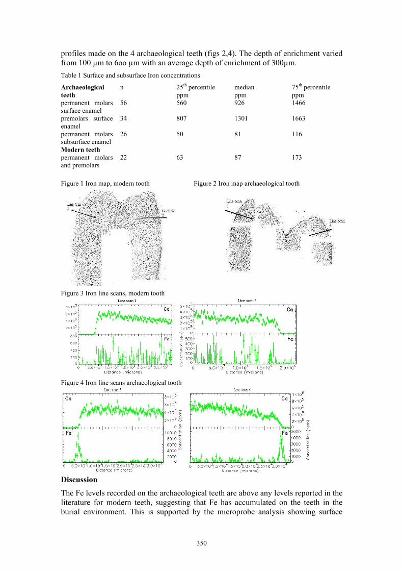
350
profiles made on the 4 archaeological teeth (figs 2,4). The depth of enrichment varied from 100 µm to 6oo µm with an average depth of enrichment of 300µm. Table 1 Surface and subsurface Iron concentrations
Archaeological teeth
n 25th percentile ppm
median ppm
75th percentile ppm
permanent molars surface enamel
56 560 926 1466
premolars surface enamel
34 807 1301 1663
permanent molars subsurface enamel
26 50 81 116
Modern teeth permanent molars and premolars
22 63 87 173
Figure 1 Iron map, modern tooth Figure 2 Iron map archaeological tooth
Figure 3 Iron line scans, modern tooth
Figure 4 Iron line scans archaeological tooth
Discussion
The Fe levels recorded on the archaeological teeth are above any levels reported in the literature for modern teeth, suggesting that Fe has accumulated on the teeth in the burial environment. This is supported by the microprobe analysis showing surface
351
enrichment in the archaeological teeth not seen in the modern teeth. The degree of enrichment shows no significant relationship with the amount of Fe in the soil or with the soil pH.
The depth of Fe accumulation in the enamel ranged from 100µm to 600 µm, therefore if the outer 600 µm of enamel was removed from the teeth, the underlying non-enriched enamel could be analysed for a biogenic Fe signal. Although in this case it was possible to completely remove the enamel from the archaeological teeth to analyse clean subsurface enamel this is quite destructive and is not generally recommended for archaeological teeth. The removal of the outer 600 µm of enamel is a far less destructive solution to measuring biogenic levels of Fe.
Conclusions
In the archaeological teeth, Fe levels in the enamel appear to have been altered by the post mortem environment. However removal of the outer 600um of enamel will result in removal of the contaminated region allowing a biogenic Fe signal to be recorded.
Acknowledgments
This work was funded by a grant from the Australian Institute of Nuclear Science and Engineering (AINSE). Thanks to Dr Denise Donlon, University of Sydney and Dr Catherine Bennett, University of Melbourne. Thanks to the University of Sydney Electron Microscope Unit, the United Dental Hospital Sydney and the Prince of Wales Destitute Children's Asylum Management Committee.
References
1. F.D. Pate and J.T. Hutton, J. of Archaeological Sci, 15 (1988) pp. 729-739.
2. J.E. Buikstra, S. Frankenberg, J.B. Lambert and X. Liang, in The Chemistry of Prehistoric Bone,
T.D. Price (ed), Cambridge University press: Cambridge. 1989 pp. 155-210.
3. 4. Sandford, M.K. and D.S. Weaver, in Biological anthropology of the human skeleton, M.A. Katzenberg and S.R. Saunders (eds), Wiley-Liss: New York ; Chichester. 2000 pp. 329-350.
4. Montgomery, J. and J. Evans, Chemistry in Britain, 36 (2000) pp. 34-36.
5. Grupe, G., in Dental anthropology: fundamentals, limits, and prospects, K.W. Alt et al. (eds) Springer Wien: New York 1998. pp 337-347.
6. Sardesai, V.M., Introduction to clinical nutrition. 2nd ed. Marcel Dekker, Inc New York. 2003. pp 109-112.
7. Brown, C.J., S. Chenery, B. Smith, C. Mason, A. Tomkins, G. Roberts, L. Sserunjogi and J. Tiberindwa Archives of Oral Biology, 49 (2004) pp. 705-717.
8. Brudevold, F. and R. Soremark, in Structural and chemical organization of teeth, A.E.W. Miles (ed), Academic Press Inc.: New York. 1967 pp. 247-277.
9. Anttila, A. and A. Anttila, Arch of Oral Biol, 32 (1987) pp. 713-7.
10. D.W. Lane and C.A. Duffy, Nucl Instr and Meth, 118 (1996): p. 392-395.
11. Solis, C., Oliver, A., RodriguezFernandez, L., Andrade, E., ChavezLomeli, M. E., Mancilla, J. & Saldivar, O. Nuc Instr & Meth Bl. 118, (1996) 1-4, pp. 359-362.
352
12. C.S. Larsen, Bioarchaeology: interpreting behavior from the human skeleton. Cambridge University Press. New York 1997 pp. 270-300
13. P. Budd, J. Montgomery, A. Cox, P. Krause, B. Barreiro and R.G. Thomas, R. G Sci of the Total Environ, 220 (1998) pp. 121-136.
14. J. Montgomery, P. Budd, A. Cox, P. Krause and R.G. Thomas, in Metals in antiquity, S.M.M. Young, et al. (eds) BAR international series Archaeopress: Oxford. 1999, pp. 290-296.
15. M.V. Stack and D.K. Whittaker, J. of Dental Res. 61 (1982) pp. 563-563.
16. R. Brenn, C. Haug, U. Klar, S. Zander, K.W. Alt, D.N. Jamieson, K.K. Lee and H. Schutkowski, Nucl Instr and Meth,. 158 (1999) pp. 270-274.
17. L. Rodriguez-Fernandez, J.L. Ruvalcaba-Sil, M.A. Ontalba-Salamanca, J.A.; Roman-Berrelleza, M.L. Gallardo, D.M. Grimaldi, O.G. de Lucio and J. Miranda, Nucl Instr and Meth, 150 (1999) pp. 663-666.
18. M.L. Carvalho, J.P. Marques, A.F. Marques and C. Casaca X-ray Spectrometry, 33 (2004) pp. 55-60.
19. J. Mansilla, C. Solis,M.E. Chavez-Lomeli and J.E. Gama, Am J. of Phys Anth, 120 (2003) pp. 73-82.
20. Godden Mackay Pty Ltd, POW Project 1995 Randwick Destitute Children's Asylum Cemetery Archaeological Investigation. Report for South Eastern Area Health Service, Heritage Council, NSW, NSW Dept of Health. 1997.
21 Williams, A-M.M. 2005 Trace Elements in 19th century Australian Children’s teeth. PhD, University of Sydney, Australia.
22. Ryan, C.G. Nucl Instr and Meth B 181 (2001) 170-179
353
Oxidation profiles of arsenic, iron, manganese and uranium in tailings dam samples using x-ray absorption near-edge structure
spectroscopy Myint Zaw
Radiopharmaceutical Research Institute, Australian Nuclear Science and Technology Organisation, PMB 1, Menai, NSW 2234, Australia.
Abstract
Synchrotron radiation experiments were performed at the Australian National Beamline Facility at Photon Factory, Tsukuba, Japan using the X-ray absorption near-edge structure spectroscopy to investigate the solid state redox speciation of arsenic, iron, manganese and uranium elements in Rum Jungle tailings dam samples. Redox speciation of these elements in tailings dam samples is important because their bioavailability, mobility, toxicity and sorption properties vary with oxidation state and chemical environment. The obtained data indicated that the oxidation states of manganese and uranium compounds varied significantly within the depth profiles whilst only slight changes were observed in the depth profiles of iron and arsenic. This technique was shown to be excellent as a tool to differentiate oxidation states of these elements within the samples. The obtained data provide valuable insights into the behaviour of waste storage and waste disposal sites.
1.Introduction
In order to understand the evolving world of environmental issues, the ability to understand and predict the stability and bioavailability of heavy metal contaminants in mine waste is becoming increasingly more important. Toxic and heavy metals are common contaminants in tailings and effluents resulting from metallurgical processing of various ores. In tailings, metals occur in various forms and oxidation states. Stability of these toxic minerals and compounds in metallurgical wastes for long-term disposal is one of the challenges facing the mining industry today.
The aim of this synchrotron experiment is to determine the oxidation depth profiles of metals such as arsenic (As), iron (Fe), manganese (Mn) and uranium (U) in a tailings storage facility using Synchrotron X-ray absorption near-edge structure (XANES) spectroscopy. The chemical form and characteristic of these elements control the bioavailability, toxicity and mobility of these metals. For example As(III) compounds are more toxic than As(V) compounds. The evaluation of the potential risks of As in mine tailings needs accurate determination of its speciation in different solid phases and its possible presence as a surface-bound or adsorbed species. The adsorbed species if present could represent a more mobile form relative to arsenic bound in solid phases.
Samples were collected from the Rum Jungle uranium mine, which is located in the monsoonal north of the Northern Territory, 64-km south of Darwin. Operations commenced in 1953 and ceased in 1971. A rehabilitation program for the mine site was started in 1982. Part of this rehabilitation program included the removal and burial of 465,000 tonnes of tailings “contained” in an area known as the Old Tailings Dam. Prior to removal, the samples from tailings dam and subsoil were sampled in May 1984 to investigate if the tailings had settled and to examine how far soluble material had been transported from the tailings to the subsoil (Lowson et al, 1987).
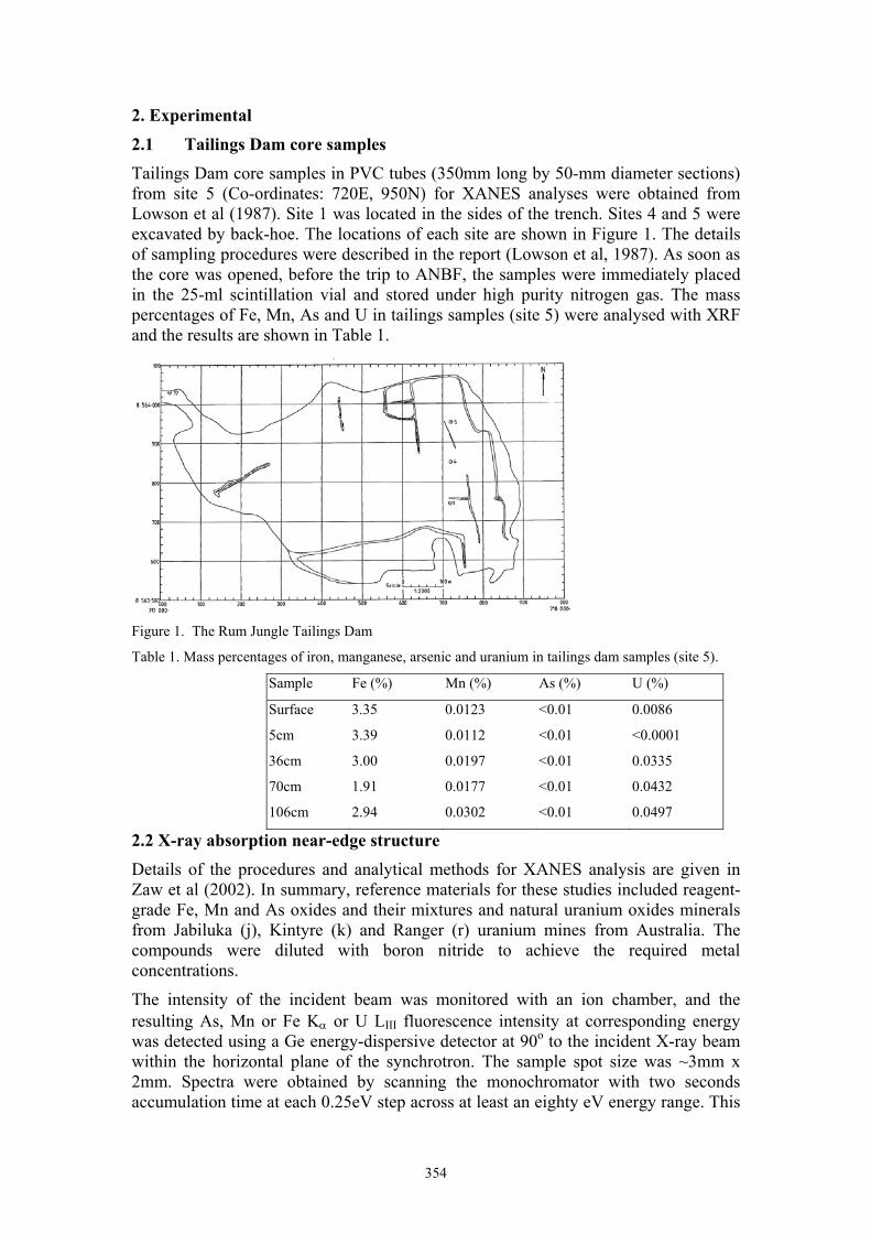
354
2. Experimental
2.1 Tailings Dam core samples
Tailings Dam core samples in PVC tubes (350mm long by 50-mm diameter sections) from site 5 (Co-ordinates: 720E, 950N) for XANES analyses were obtained from Lowson et al (1987). Site 1 was located in the sides of the trench. Sites 4 and 5 were excavated by back-hoe. The locations of each site are shown in Figure 1. The details of sampling procedures were described in the report (Lowson et al, 1987). As soon as the core was opened, before the trip to ANBF, the samples were immediately placed in the 25-ml scintillation vial and stored under high purity nitrogen gas. The mass percentages of Fe, Mn, As and U in tailings samples (site 5) were analysed with XRF and the results are shown in Table 1.
Figure 1. The Rum Jungle Tailings Dam
Table 1. Mass percentages of iron, manganese, arsenic and uranium in tailings dam samples (site 5).
Sample Fe (%) Mn (%) As (%) U (%)
Surface 3.35 0.0123 <0.01 0.0086
5cm 3.39 0.0112 <0.01 <0.0001
36cm 3.00 0.0197 <0.01 0.0335
70cm 1.91 0.0177 <0.01 0.0432
106cm 2.94 0.0302 <0.01 0.0497
2.2 X-ray absorption near-edge structure
Details of the procedures and analytical methods for XANES analysis are given in Zaw et al (2002). In summary, reference materials for these studies included reagent-grade Fe, Mn and As oxides and their mixtures and natural uranium oxides minerals from Jabiluka (j), Kintyre (k) and Ranger (r) uranium mines from Australia. The compounds were diluted with boron nitride to achieve the required metal concentrations.
The intensity of the incident beam was monitored with an ion chamber, and the resulting As, Mn or Fe Kα or U LIII fluorescence intensity at corresponding energy was detected using a Ge energy-dispersive detector at 90o to the incident X-ray beam within the horizontal plane of the synchrotron. The sample spot size was ~3mm x 2mm. Spectra were obtained by scanning the monochromator with two seconds accumulation time at each 0.25eV step across at least an eighty eV energy range. This
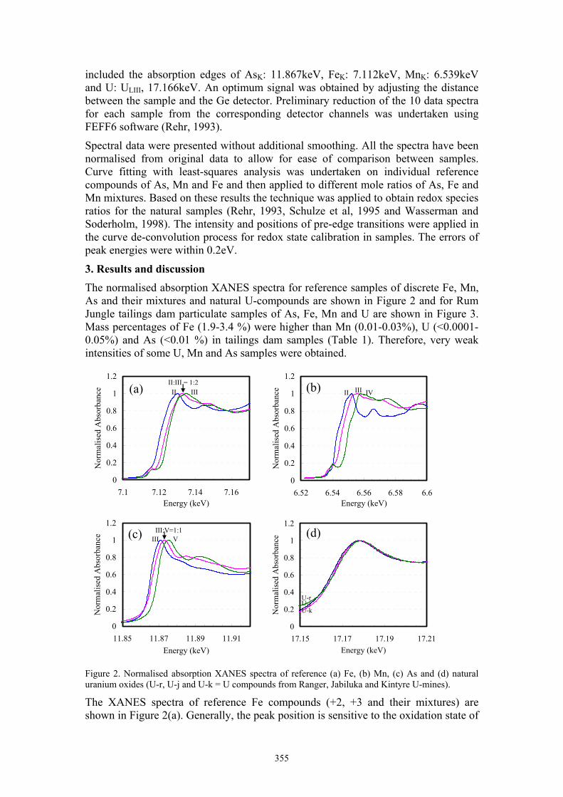
355
included the absorption edges of AsK: 11.867keV, FeK: 7.112keV, MnK: 6.539keV and U: ULIII, 17.166keV. An optimum signal was obtained by adjusting the distance between the sample and the Ge detector. Preliminary reduction of the 10 data spectra for each sample from the corresponding detector channels was undertaken using FEFF6 software (Rehr, 1993).
Spectral data were presented without additional smoothing. All the spectra have been normalised from original data to allow for ease of comparison between samples. Curve fitting with least-squares analysis was undertaken on individual reference compounds of As, Mn and Fe and then applied to different mole ratios of As, Fe and Mn mixtures. Based on these results the technique was applied to obtain redox species ratios for the natural samples (Rehr, 1993, Schulze et al, 1995 and Wasserman and Soderholm, 1998). The intensity and positions of pre-edge transitions were applied in the curve de-convolution process for redox state calibration in samples. The errors of peak energies were within 0.2eV.
3. Results and discussion
The normalised absorption XANES spectra for reference samples of discrete Fe, Mn, As and their mixtures and natural U-compounds are shown in Figure 2 and for Rum Jungle tailings dam particulate samples of As, Fe, Mn and U are shown in Figure 3. Mass percentages of Fe (1.9-3.4 %) were higher than Mn (0.01-0.03%), U (<0.0001- 0.05%) and As (<0.01 %) in tailings dam samples (Table 1). Therefore, very weak intensities of some U, Mn and As samples were obtained.
0
0.2
0.4
0.6
0.8
1
1.2
11.85 11.87 11.89 11.91Energy (keV)
Nor
mal
ised
Abs
orba
nce III:V=1:1
III V(c)
0
0.2
0.4
0.6
0.8
1
1.2
6.52 6.54 6.56 6.58 6.6Energy (keV)
Nor
mal
ised
Abs
orba
nce (b) II IVIII
0
0.2
0.4
0.6
0.8
1
1.2
7.1 7.12 7.14 7.16Energy (keV)
Nor
mal
ised
Abs
orba
nce (a) II:III = 1:2
IIIII
0
0.2
0.4
0.6
0.8
1
1.2
17.15 17.17 17.19 17.21Energy (keV)
Nor
mal
ised
Abs
orba
nce
U-kU-jU-r
(d)
Figure 2. Normalised absorption XANES spectra of reference (a) Fe, (b) Mn, (c) As and (d) natural uranium oxides (U-r, U-j and U-k = U compounds from Ranger, Jabiluka and Kintyre U-mines).
The XANES spectra of reference Fe compounds (+2, +3 and their mixtures) are shown in Figure 2(a). Generally, the peak position is sensitive to the oxidation state of
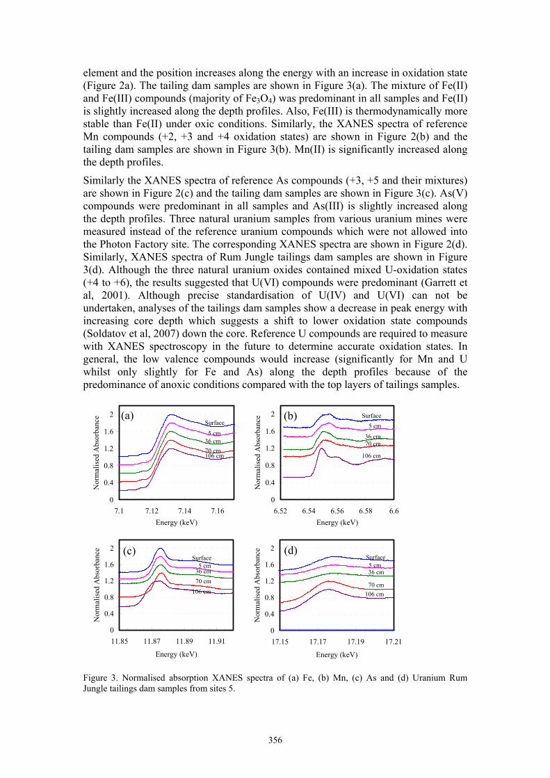
356
element and the position increases along the energy with an increase in oxidation state (Figure 2a). The tailing dam samples are shown in Figure 3(a). The mixture of Fe(II) and Fe(III) compounds (majority of Fe3O4) was predominant in all samples and Fe(II) is slightly increased along the depth profiles. Also, Fe(III) is thermodynamically more stable than Fe(II) under oxic conditions. Similarly, the XANES spectra of reference Mn compounds (+2, +3 and +4 oxidation states) are shown in Figure 2(b) and the tailing dam samples are shown in Figure 3(b). Mn(II) is significantly increased along the depth profiles.
Similarly the XANES spectra of reference As compounds (+3, +5 and their mixtures) are shown in Figure 2(c) and the tailing dam samples are shown in Figure 3(c). As(V) compounds were predominant in all samples and As(III) is slightly increased along the depth profiles. Three natural uranium samples from various uranium mines were measured instead of the reference uranium compounds which were not allowed into the Photon Factory site. The corresponding XANES spectra are shown in Figure 2(d). Similarly, XANES spectra of Rum Jungle tailings dam samples are shown in Figure 3(d). Although the three natural uranium oxides contained mixed U-oxidation states (+4 to +6), the results suggested that U(VI) compounds were predominant (Garrett et al, 2001). Although precise standardisation of U(IV) and U(VI) can not be undertaken, analyses of the tailings dam samples show a decrease in peak energy with increasing core depth which suggests a shift to lower oxidation state compounds (Soldatov et al, 2007) down the core. Reference U compounds are required to measure with XANES spectroscopy in the future to determine accurate oxidation states. In general, the low valence compounds would increase (significantly for Mn and U whilst only slightly for Fe and As) along the depth profiles because of the predominance of anoxic conditions compared with the top layers of tailings samples.
0
0.4
0.8
1.2
1.6
2
7.1 7.12 7.14 7.16Energy (keV)
Nor
mal
ised
Abs
orba
nce (a)
Surface
5 cm
106 cm70 cm36 cm
0
0.4
0.8
1.2
1.6
2
6.52 6.54 6.56 6.58 6.6Energy (keV)
Nor
mal
ised
Abs
orba
nce (b) Surface
70 cm
106 cm
36 cm
5 cm
0
0.4
0.8
1.2
1.6
2
11.85 11.87 11.89 11.91
Energy (keV)
Nor
mal
ised
Abs
orba
nce (c)
106 cm70 cm36 cm5 cm
Surface
0
0.4
0.8
1.2
1.6
2
17.15 17.17 17.19 17.21
Energy (keV)
Nor
mal
ised
Abs
orba
nce
Surface 5 cm
106 cm 70 cm
36 cm
(d)
Figure 3. Normalised absorption XANES spectra of (a) Fe, (b) Mn, (c) As and (d) Uranium Rum Jungle tailings dam samples from sites 5.
357
4. Conclusions
The results of this work show that the synchrotron XANES technique is well-suited to examining the solid state redox speciation of arsenic, iron, manganese and uranium elements in Rum Jungle tailings dam samples. The obtained data indicated that the oxidation states of Mn and U compounds varied significantly within the depth profiles whilst only slight changes were observed in the depth profiles of iron and arsenic. Further work is required to complete the analysis of reference U-samples if authorisation for transport and entry of samples to ANBF can be obtained. The obtained data provide valuable insights into the behaviour of waste storage and waste disposal sites.
Acknowledgments
This work was undertaken at the Australian National Beamline Facility with financial support from the Australian Synchrotron Research Program (ASRP), which is funded by the Commonwealth of Australia under the Major National Research Facilities Program. The author gives special thanks to Dr R. Lowson who helped initiate the work and provided dam samples, N. Blagojevic and Dr G. Foran for their assistance at ANBF and acknowledges valuable input from R. Szymczak (ANSTO).
References Garrett, R. F., Blagojevic, N., Cai, Z., Lai, B., Legnini, D. G., Rodrigues, W and Stampfl, A. P. J.
Synchrotron X-ray microprobe analysis of radioactive trace elements in mineral sands. Nucl. Instr. Meth. Phys. Res. A 467-468 (2001) 897-900.
Lowson, R. T., Evans, J. V., Sarbutt, J. V., Sinclair, G. and Folk, E. The Rum Jungle Tailings Dam – Chemical Profile of the Subsoil. Australian Nuclear Science and Technology Organisation, ANSTO/E663, (1987) 59 pp.
Rehr, J. J. Recent Developments in Multi-Scattering Calculations of XAFS and XANES. Jpn, J. Appl. Phys, 32, Suppl. 32-2 (1993), 8-12.
Schulze, D. G., Sutton, S. R. and Bajt, S. Determining Manganese Oxidation State in Soils using X-ray Absorption Near-edge Structure Spectroscopy. Soil Sci. Soc. Am. J. 59 (1995) 1540-1548.
Soldatov, A. V., Lamoen, D., Konstantinović, M. J., Berghe, S. Van den, Scheinost, A. C. and Verwerft, M. Local structure and oxidation state of uranium in some ternary oxides: X-ray absorption analysis. J. Solid State Chem. 180 (2007) 54-61.
Wasserman, S. R. and Soderholm, L. Effect of Surface Modification on the Interlayer Chemistry of Iron in a Smectite Clay. Chem. Mater. 10, (1998) 559-566.
Zaw, M., Szymczak, R. and Twining, J. Application of synchrotron radiation technique to analysis of environmental samples. Nucl. Instr. Meth. Phys. Res. B 190 (2002) 856-859.
358
Reduction of titanium dioxide: comparison of analysis by raman spectroscopy and XRD
Waven Zhang 1, Jeffrey McCallum2, David Sadedin1, Markus Reuter3 1 Department of Chemical & Biomolecular Engineering, The University of Melbourne
2 School of Physics, The University of Melbourne 3 AusMelt Pty Ltd.
The reduction of metal oxides using hydrogen presents several potential advantages: (1) hydrogen is readily available, being the most abundant element in the universe [1]; (2) the reaction is far more environmentally friendly, with the by-product being water; (3) atomic hydrogen (H), is theoretically a very powerful reductant that can reduce most oxides at temperatures below the metal melting point. Given the thermodynamic ability of atomic hydrogen to reduce metal oxides and concerns on CO2 emission from existing metal production techniques, atomic hydrogen reduction is worth critical exploration.
Titanium metal is sometimes known as a “space-age metal” [2] because of its various exceptional properties. It has a high strength to weight ratio, being as strong as steel but 45% lighter[3]; it is incredibly corrosion resistant, being able to withstand all naturally occurring corrosive environments [2, 3].
Yet, despite the unique properties of titanium and its abundance as a mineral in the ground [4, 5], the usage of titanium metal and its alloys are predominantly limited to the aerospace industry and the military. The expense of the metal, most of which is incurred in its extraction, prevents its wider usage.
Currently, the world's metallic titanium supply is produced via the Kroll method. In this method, 361MJ is required to produce one kilogram of titanium compared to 23MJ for the production of steel [6]. If the global warming potential is considered, then 35.7kg of CO2 gas equivalent is produced for every kilogram of titanium produced, compared to 2.3kg for that of steel. For both the economic and environmental reasons, another method to produce titanium metal is desired, one that is cheaper and more efficient, both economically and environmentally.
There are several publications on hydrogen plasma reduction of titanium dioxide in a range of experimental conditions [7-15]. Low and atmospheric pressure plasmas have been used, with hydrogen partial pressure ranging from 1% to 95%. Experimental setup includes both ‘in-flight’, where reactant particles are injected into the plasma with the reducing gas, and batch process, where the plasma is directed onto a crucible where the reactants sit. Both the rutile and anatase form of TiO2 have been used, with Ti3O5, Ti2O3, and occasionally TiO found in reaction products; although the presence of carbon seems to be required for reduction to TiO.
The reduction reaction TiO2 + H → TiH2, is most thermodynamically favourable (up to 2000°C) when compared to reduction to Ti or any titanium oxides. However, the TiH2 product has never been reported in literature.
Currently the Department of Chemical & Biomolecular Engineering in conjunction with the School of Physics, both at The University of Melbourne, are examining hydrogen atom interactions with TiO2, with the aim of improving the understanding of the interactions and thus determining the limitations of hydrogen reduction of titanium oxides. Here we report the results obtained from Raman and X-Ray Diffraction (XRD) analysis, and discuss apparent inconsistencies between them and what this may indicate.
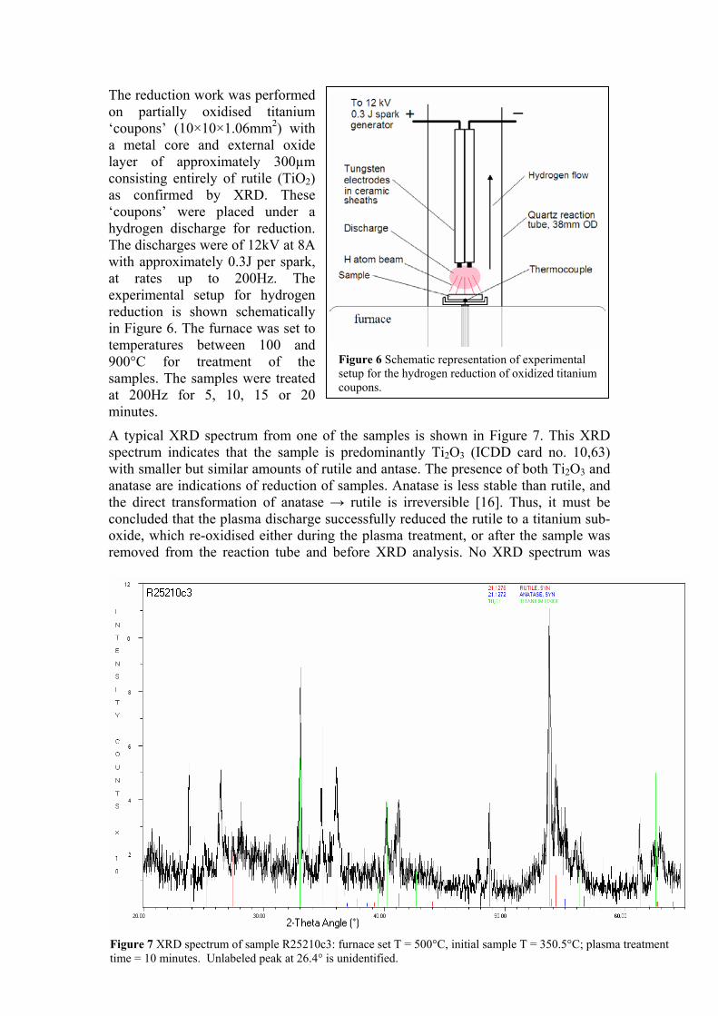
359
The reduction work was performed on partially oxidised titanium ‘coupons’ (10×10×1.06mm2) with a metal core and external oxide layer of approximately 300µm consisting entirely of rutile (TiO2) as confirmed by XRD. These ‘coupons’ were placed under a hydrogen discharge for reduction. The discharges were of 12kV at 8A with approximately 0.3J per spark, at rates up to 200Hz. The experimental setup for hydrogen reduction is shown schematically in Figure 6. The furnace was set to temperatures between 100 and 900°C for treatment of the samples. The samples were treated at 200Hz for 5, 10, 15 or 20 minutes.
A typical XRD spectrum from one of the samples is shown in Figure 7. This XRD spectrum indicates that the sample is predominantly Ti2O3 (ICDD card no. 10,63) with smaller but similar amounts of rutile and antase. The presence of both Ti2O3 and anatase are indications of reduction of samples. Anatase is less stable than rutile, and the direct transformation of anatase → rutile is irreversible [16]. Thus, it must be concluded that the plasma discharge successfully reduced the rutile to a titanium sub-oxide, which re-oxidised either during the plasma treatment, or after the sample was removed from the reaction tube and before XRD analysis. No XRD spectrum was
Figure 7 XRD spectrum of sample R25210c3: furnace set T = 500°C, initial sample T = 350.5°C; plasma treatment time = 10 minutes. Unlabeled peak at 26.4° is unidentified.
Figure 6 Schematic representation of experimental setup for the hydrogen reduction of oxidized titanium coupons.
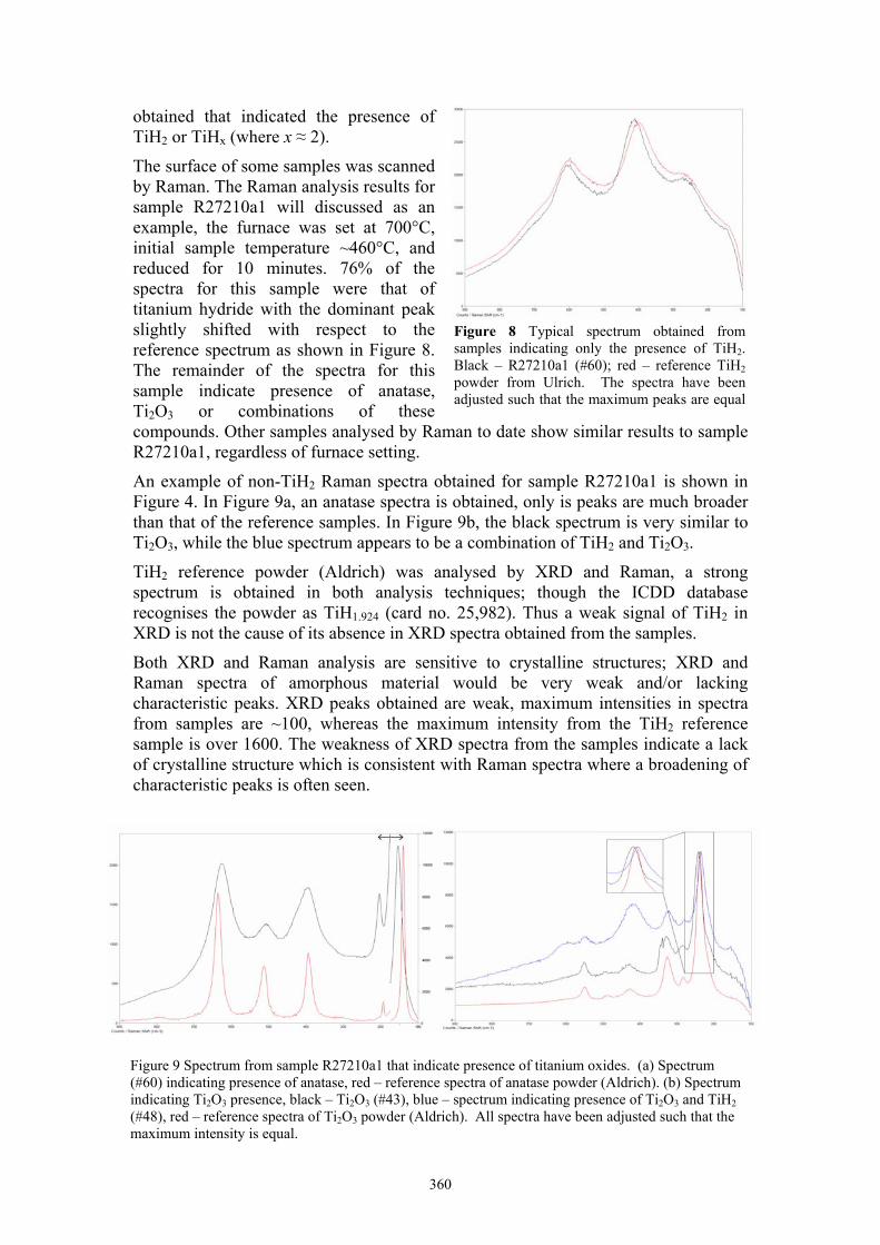
360
obtained that indicated the presence of TiH2 or TiHx (where x ≈ 2).
The surface of some samples was scanned by Raman. The Raman analysis results for sample R27210a1 will discussed as an example, the furnace was set at 700°C, initial sample temperature ~460°C, and reduced for 10 minutes. 76% of the spectra for this sample were that of titanium hydride with the dominant peak slightly shifted with respect to the reference spectrum as shown in Figure 8. The remainder of the spectra for this sample indicate presence of anatase, Ti2O3 or combinations of these compounds. Other samples analysed by Raman to date show similar results to sample R27210a1, regardless of furnace setting.
An example of non-TiH2 Raman spectra obtained for sample R27210a1 is shown in Figure 4. In Figure 9a, an anatase spectra is obtained, only is peaks are much broader than that of the reference samples. In Figure 9b, the black spectrum is very similar to Ti2O3, while the blue spectrum appears to be a combination of TiH2 and Ti2O3.
TiH2 reference powder (Aldrich) was analysed by XRD and Raman, a strong spectrum is obtained in both analysis techniques; though the ICDD database recognises the powder as TiH1.924 (card no. 25,982). Thus a weak signal of TiH2 in XRD is not the cause of its absence in XRD spectra obtained from the samples.
Both XRD and Raman analysis are sensitive to crystalline structures; XRD and Raman spectra of amorphous material would be very weak and/or lacking characteristic peaks. XRD peaks obtained are weak, maximum intensities in spectra from samples are ~100, whereas the maximum intensity from the TiH2 reference sample is over 1600. The weakness of XRD spectra from the samples indicate a lack of crystalline structure which is consistent with Raman spectra where a broadening of characteristic peaks is often seen.
Figure 8 Typical spectrum obtained from samples indicating only the presence of TiH2. Black – R27210a1 (#60); red – reference TiH2powder from Ulrich. The spectra have been adjusted such that the maximum peaks are equal
Figure 9 Spectrum from sample R27210a1 that indicate presence of titanium oxides. (a) Spectrum (#60) indicating presence of anatase, red – reference spectra of anatase powder (Aldrich). (b) Spectrum indicating Ti2O3 presence, black – Ti2O3 (#43), blue – spectrum indicating presence of Ti2O3 and TiH2 (#48), red – reference spectra of Ti2O3 powder (Aldrich). All spectra have been adjusted such that the maximum intensity is equal.

361
Lastly, the penetration of light and x-rays into samples are vastly different. It is expected that the reduction of TiO2 to TiH2 would take place on the surface. It is possible that the reduction of TiO2 to TiH2 is only occurring in a very thin surface layer on the sample, and is not being detected in the XRD. Currently, we are trying to quantify this.
In conclusion, Raman analysis of titanium dioxide samples that had been treated in a hydrogen discharge has consistently shown strong presence of TiH2 in the samples, which was not observed in XRD analysis.
References 1. Carter, T.J. and L.A. Cornish, Hydrogen in metals. Engineering Failure Analysis, 2001. 8(2): p.
113-121.
2. Knittel, D., Titanium and Titanium Alloys, in Kirk-Othmer Encyclopedia of Chemical Technology, H.F. Mark, et al., Editors. 1983, A Wiley-Interscience Publication: John Wiley & Sons: New York.
3. Titanium. [cited 4th May, 2005]; Available from: http://en.wikipedia.org/wiki/Titanium.
4. Lutjering, G. and J. Williams, Titanium. 2003, New York: Springer.
5. Titanium: Past, Present, and Future; Report of the Panel on Assessment of Titanium Availability: Current and Future Needs of the Committee on Technical Aspects of Critical and Strategic Materials. Vol. http://www.nap.edu/books/POD140/html; accessed 23/06/2005. 1983, Washington, DC: National Academic Press.
6. Norgate, T.E., V. Rajakumar, and S. Trang, Titanium and other light metals - technology pathways to sustainable development. Publications of the Australasian Institute of Mining and Metallurgy, 2004. 2/2004: p. 105-112.
7. Bullard, D.E. and D.C. Lynch, Reduction of titanium dioxide in a non-equilibrium hydrogen plasma. Metallurgical and Materials Transactions B-Process Metallurgy and Materials Processing Science, 1997. 28(6): p. 1069-1080.
8. Palmer, R.A., et al., Reduction of TiO2 with hydrogen plasma. Plasma Chemistry and Plasma Processing, 2002. 22(3): p. 335-350.
9. Kitamura, T., K. Shibata, and K. Takeda, In-Flight Reduction of Fe2O3, Cr2O3, TiO2 and Al2O3 by Ar-H2 and Ar-Ch4 Plasma. Isij International, 1993. 33(11): p. 1150-1158.
10. Zhang, G.Q. and O. Ostrovski, Reduction of titania by methane-hydrogen-argon gas mixture. Metallurgical and Materials Transactions B-Process Metallurgy and Materials Processing Science, 2000. 31(1): p. 129-139.
11. Kitamura, T., K. Shibata, and K. Takeda. In-Flight Reduction of Fe2O3, Cr2O3, TiO2 and Al2O3 by Ar-H2 Plasma. in Thermal Plasma Applications in Materials and Metallurgical Processing. 1992. San Diego, California; USA.
12. Rekoske, J.E. and M.A. Barteau, Isothermal reduction kinetics of titanium dioxide-based materials. Journal of Physical Chemistry B, 1997. 101(7): p. 1113-1124.
13. Huet, S., et al., Reduction of TiO2 assisted by a microwave plasma at atmospheric pressure. Thin Solid Films, 2005. 475(1-2 SPEC ISS): p. 63-67.
14. Bouzoubaa, A., et al., Comparison of the reduction of metal oxide surfaces: TiO2-anatase, TiO2-rutile and SnO2-rutile. Surface Science, 2005. 583(1): p. 107-117.
15. Degout, D., F. Kassabji, and P. Fauchais, Titanium dioxide plasma treatment. Plasma Chemistry and Plasma Processing, 1984. 4(3): p. 179-98.
16. Navrotsky, A. and O.J. Kleppa, Enthalpy of the Anatase-Rutile Transformation. Journal of the American Ceramic Society, 1967. 50(11): p. 626-626.
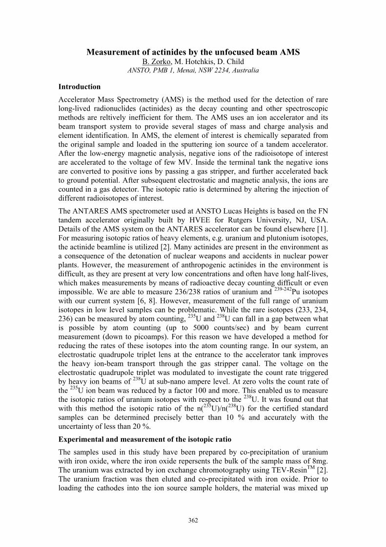
362
Measurement of actinides by the unfocused beam AMS B. Zorko, M. Hotchkis, D. Child
ANSTO, PMB 1, Menai, NSW 2234, Australia
Introduction
Accelerator Mass Spectrometry (AMS) is the method used for the detection of rare long-lived radionuclides (actinides) as the decay counting and other spectroscopic methods are reltively inefficient for them. The AMS uses an ion accelerator and its beam transport system to provide several stages of mass and charge analysis and element identification. In AMS, the element of interest is chemically separated from the original sample and loaded in the sputtering ion source of a tandem accelerator. After the low-energy magnetic analysis, negative ions of the radioisotope of interest are accelerated to the voltage of few MV. Inside the terminal tank the negative ions are converted to positive ions by passing a gas stripper, and further accelerated back to ground potential. After subsequent electrostatic and magnetic analysis, the ions are counted in a gas detector. The isotopic ratio is determined by altering the injection of different radioisotopes of interest.
The ANTARES AMS spectrometer used at ANSTO Lucas Heights is based on the FN tandem accelerator originally built by HVEE for Rutgers University, NJ, USA. Details of the AMS system on the ANTARES accelerator can be found elsewhere [1]. For measuring isotopic ratios of heavy elements, e.g. uranium and plutonium isotopes, the actinide beamline is utilized [2]. Many actinides are present in the environment as a consequence of the detonation of nuclear weapons and accidents in nuclear power plants. However, the measurement of anthropogenic actinides in the environment is difficult, as they are present at very low concentrations and often have long half-lives, which makes measurements by means of radioactive decay counting difficult or even impossible. We are able to measure 236/238 ratios of uranium and 239-242Pu isotopes with our current system [6, 8]. However, measurement of the full range of uranium isotopes in low level samples can be problematic. While the rare isotopes (233, 234, 236) can be measured by atom counting, 235U and 238U can fall in a gap between what is possible by atom counting (up to 5000 counts/sec) and by beam current measurement (down to picoamps). For this reason we have developed a method for reducing the rates of these isotopes into the atom counting range. In our system, an electrostatic quadrupole triplet lens at the entrance to the accelerator tank improves the heavy ion-beam transport through the gas stripper canal. The voltage on the electrostatic quadrupole triplet was modulated to investigate the count rate triggered by heavy ion beams of 238U at sub-nano ampere level. At zero volts the count rate of the 235U ion beam was reduced by a factor 100 and more. This enabled us to measure the isotopic ratios of uranium isotopes with respect to the 238U. It was found out that with this method the isotopic ratio of the n(235U)/n(238U) for the certified standard samples can be determined precisely better than 10 % and accurately with the uncertainty of less than 20 %.
Experimental and measurement of the isotopic ratio
The samples used in this study have been prepared by co-precipitation of uranium with iron oxide, where the iron oxide repersents the bulk of the sample mass of 8mg. The uranium was extracted by ion exchange chromotography using TEV-ResinTM [2]. The uranium fraction was then eluted and co-precipitated with iron oxide. Prior to loading the cathodes into the ion source sample holders, the material was mixed up
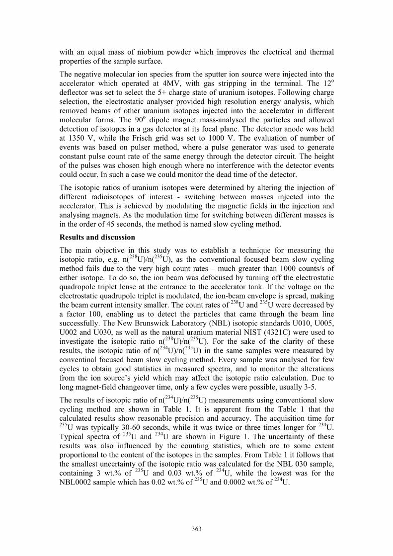
363
with an equal mass of niobium powder which improves the electrical and thermal properties of the sample surface.
The negative molecular ion species from the sputter ion source were injected into the accelerator which operated at 4MV, with gas stripping in the terminal. The 12o deflector was set to select the 5+ charge state of uranium isotopes. Following charge selection, the electrostatic analyser provided high resolution energy analysis, which removed beams of other uranium isotopes injected into the accelerator in different molecular forms. The 90o dipole magnet mass-analysed the particles and allowed detection of isotopes in a gas detector at its focal plane. The detector anode was held at 1350 V, while the Frisch grid was set to 1000 V. The evaluation of number of events was based on pulser method, where a pulse generator was used to generate constant pulse count rate of the same energy through the detector circuit. The height of the pulses was chosen high enough where no interference with the detector events could occur. In such a case we could monitor the dead time of the detector.
The isotopic ratios of uranium isotopes were determined by altering the injection of different radioisotopes of interest - switching between masses injected into the accelerator. This is achieved by modulating the magnetic fields in the injection and analysing magnets. As the modulation time for switching between different masses is in the order of 45 seconds, the method is named slow cycling method.
Results and discussion
The main objective in this study was to establish a technique for measuring the isotopic ratio, e.g. n(238U)/n(235U), as the conventional focused beam slow cycling method fails due to the very high count rates – much greater than 1000 counts/s of either isotope. To do so, the ion beam was defocused by turning off the electrostatic quadropole triplet lense at the entrance to the accelerator tank. If the voltage on the electrostatic quadrupole triplet is modulated, the ion-beam envelope is spread, making the beam current intensity smaller. The count rates of 238U and 235U were decreased by a factor 100, enabling us to detect the particles that came through the beam line successfully. The New Brunswick Laboratory (NBL) isotopic standards U010, U005, U002 and U030, as well as the natural uranium material NIST (4321C) were used to investigate the isotopic ratio n(238U)/n(235U). For the sake of the clarity of these results, the isotopic ratio of n(234U)/n(235U) in the same samples were measured by conventinal focused beam slow cycling method. Every sample was analysed for few cycles to obtain good statistics in measured spectra, and to monitor the alterations from the ion source’s yield which may affect the isotopic ratio calculation. Due to long magnet-field changeover time, only a few cycles were possible, usually 3-5.
The results of isotopic ratio of n(234U)/n(235U) measurements using conventional slow cycling method are shown in Table 1. It is apparent from the Table 1 that the calculated results show reasonable precision and accuracy. The acquisition time for 235U was typically 30-60 seconds, while it was twice or three times longer for 234U. Typical spectra of 235U and 234U are shown in Figure 1. The uncertainty of these results was also influenced by the counting statistics, which are to some extent proportional to the content of the isotopes in the samples. From Table 1 it follows that the smallest uncertainty of the isotopic ratio was calculated for the NBL 030 sample, containing 3 wt.% of 235U and 0.03 wt.% of 234U, while the lowest was for the NBL0002 sample which has 0.02 wt.% of 235U and 0.0002 wt.% of 234U.
364
Table 1: Measured and expected isotopic ratio of n(234U)/n(235U) for different isotopic standard samples treated by conventional slow cycling method
Sample Expected isotopic
ratio
Measured isotopic ratio Relative isotopic
ratio NBL005 0.00671 0.00594 ± 0.00095 0.885 NBL010 0.00539 0.00570 ± 0.00074 1.058 NBL030 0.00914 0.00849 ± 0.00085 0.929
NIST 0.00730 0.00730 ± 0.00088 1.000 NBL002 0.00909 0.00851 ± 0.00213 0.936
0 500 1000 1500 2000 2500 3000 3500 40000
50
100
150
234U
235U
measured peakpulser peak
Cou
nts
Channel number
235U 234U
Figure 1: Energy spectra of 234U and 235U measured by conventional slow cycling method for the NIST sample.
After measuring the n(234U)/n(235U) isotopic ratio for a given sample, the experiment was set for an isotopic ratio n(238U)/n(235U) measurement. The results obtained by the unfocused technique are collected in Table 2. From Table 2 it follows that the average n(238U)/n(235U) isotopic ratio for different standard samples was determined as precise as 3 % of the expected value, at maximum by 16 %. The acquisition time for 238U was typically 30 s, and, for 235U, 60 to 240 s. The uncertainty of the results obtained by the beam defocused technique was less accurate than the measurements performed by the focused beam slow cycling, and they were found to be scattered by 20 % from the average value.
In a few cases we also evaluated the n(234U)/n(235U) isotopic ratio using unfocused beam technique. These results are shown in Table 3. It is apparent from the Table 3 that the results in these cases are less precise and accurate as the results from the n(238U)/n(235U) measurement. The precision increased to 20 %, and the uncertainty could be as high as 30 %. Poorer precision and accuracy in the results can be explained by low counting statistics in measured spectra.

365
Table 2: Measured and expected isotopic ratio of n(238U)/n(235U) for different isotopic standard samples treated by unfocused beam slow cycling method.
Sample Expected isotopic
ratio
Measured isotopic ratio Relative isotopic
ratio NBL005 196.46 174.53 ± 31.416 0.888 NBL010 98.62 112.23 ± 22.460 1.139 NBL030 31.88 36.89 ± 10.699 1.157 NBL030 31.88 31.69 ± 3.169 0.994 NIST 141.04 142.92 ± 14.292 1.013 NBL005 196.463 197.75 ± 19.775 1.007 Table 3: Measured and expected isotopic ratio of n(234U)/n(235U) for different isotopic standard samples treated by unfocused beam slow slow cycling method.
Sample Expected
isotopic ratio
Measured isotopic ratio Relative isotopic
ratio NBL030 0.00914 0.0115 ± 0.00265 1.262 NBL030 0.00914 0.0110 ± 0.00074 1.210 NIST 0.00730 0.0074 ± 0.00085 1.015 NBL005 0.00671 0.0088 ± 0.00294 1.310 NBL010 0.00539 0.0070 ± 0.00229 1.298 Conclusions
We have established an ion-beam defocused technique which can be used to measure isotopic ratios of heavy isotopes, if their count rates are too high for the conventional focused beam technique. In this paper it was shown that isotopic ratio of n(238U)/n(235U), in a mass range up to few tens of picograms of the material, can be determined as precise as 3 % with the accuracy of 20 % or better. Those two features of the unfocused method give us motivation further to improve the accuracy as well as the reproducibility and repeatability.
References
[1] D. Fink , M. Hotchkis, Q. Hua, G. Jacobsen, A.M. Smith, U. Zoppi, D. Child, C. Mifsud, H. van der Gaast, A. Williams, M. Williams, Nuclear Instruments and Methods in Physics Research B 223–224 (2004) 109–115
[2] M.A.C. Hotchkis, D. Child, D. Fink, G.E. Jacobsen, P.J. Lee, N. Mino, A.M. Smith, C. Tuniz, Nucl. Instr. and Meth. B 172 (2000) 659.
[3] X.-L. Zhao, M.-J. Nadeau, L.R. Kilius, A.E. Litherland, Nucl. Instr. and Meth. B92 (1994) 249.
[4] L.K. Fifield, R.G. Cresswell, M.L. di Tada, T.R. Ophel, J.P. Day, A.P. Clacher, S.J. King, N.D. Priest, Nucl. Instr.and Meth. B 117 (1996) 295.
[5] X.-L. Zhao, L.R. Kilius, A.E. Litherland, T. Beasley, Nucl. Instr. and Meth. B 126 (1997) 297.
[6] C. Wallner, T. Faestermann, U. Gerstmann, W. Hillebrandt, K. Knie, G. Korschinek, C. Lierse, C. Pomar, G. Rugel, Nucl. Instr. and Meth. B 172 (2000) 333.
[7] T.A. Brown, A.A. Marchetti, R.E. Martinelli, C.C. Cox, J.P. Knezovich, T.F. Hamilton, Nucl. Instr. and Meth. B 223–224 (2004) 788.
[8] D.P. Child, M.A.C. Hotchkis, M.L. Williams, to be published.