Embed Size (px)
Citation preview
144 IEEE JOURNAL OF SOLID-STATE CIRCUITS, VOL. 40, NO. 1, JANUARY 2005
Millimeter-Wave CMOS DesignChinh H. Doan, Student Member, IEEE, Sohrab Emami, Student Member, IEEE, Ali M. Niknejad, Member, IEEE,
and Robert W. Brodersen, Fellow, IEEE
Abstract—This paper describes the design and modeling ofCMOS transistors, integrated passives, and circuit blocks atmillimeter-wave (mm-wave) frequencies. The effects of parasiticson the high-frequency performance of 130-nm CMOS transistorsare investigated, and a peak max of 135 GHz has been achievedwith optimal device layout. The inductive quality factor ( )is proposed as a more representative metric for transmissionlines, and for a standard CMOS back-end process, coplanarwaveguide (CPW) lines are determined to possess a higherthan microstrip lines. Techniques for accurate modeling of activeand passive components at mm-wave frequencies are presented.The proposed methodology was used to design two widebandmm-wave CMOS amplifiers operating at 40 GHz and 60 GHz.The 40-GHz amplifier achieves a peak S21 = 19 dB, outputP1dB = 0 9 dBm, IIP3 = 7 4 dBm, and consumes 24 mAfrom a 1.5-V supply. The 60-GHz amplifier achieves a peakS21 = 12 dB, output P1dB = +2 0 dBm, NF = 8 8 dB, and
consumes 36 mA from a 1.5-V supply. The amplifiers were fab-ricated in a standard 130-nm 6-metal layer bulk-CMOS process,demonstrating that complex mm-wave circuits are possible intoday’s mainstream CMOS technologies.
Index Terms—CMOS millimeter-wave integrated circuits,coplanar waveguides, max, integrated circuit modeling,high-speed integrated circuits, millimeter-wave amplifiers,Q-factor, transmission lines, wideband amplifiers.
I. INTRODUCTION
I N THE last few years, 7 GHz of contiguous bandwidth havebeen opened for unlicensed use at millimeter-wave (mm-
wave) frequencies around 60 GHz in the U.S. (57–64 GHz) andJapan (59–66 GHz). This allows for a variety of applicationsincluding gigabit/s point-to-point links, wireless local area net-works (WLANs) with extraordinary capacity, short-range highdata-rate wireless personal area networks (WPANs), and vehic-ular radar. In order for these applications to meet marketplacerequirements, the cost, size, and power consumption of any so-lution has to be significantly below what is being achieved todayusing compound semiconductor technology. Thus, an alterna-tive approach is required, such as using a mainstream digital130-nm bulk-CMOS process.
Historically, monolithic microwave integrated circuits(MMICs) have been designed using III-V semiconductortechnologies, such as GaAs and InP, which have superiorperformance compared to CMOS due to their higher electron
Manuscript received April 20, 2004; revised June 14, 2004. This workwas supported in part by the Army Communications-Electronics Command(CECOM) Contract DAAB07-02-1-L428 and the industrial members of theBerkeley Wireless Research Center.
The authors are with the Berkeley Wireless Research Center, Uni-versity of California, Berkeley, CA 94704 USA (e-mail: [email protected]; [email protected]; [email protected];[email protected]).
Digital Object Identifier 10.1109/JSSC.2004.837251
mobility, higher breakdown voltage, and the availability ofhigh quality-factor passives. Still, a CMOS implementa-tion promises higher levels of integration and reduced cost.Several recent developments have combined to enable CMOScircuit blocks to operate at ever-increasing frequencies. First,mm-wave CMOS circuits directly benefit from the higherspeed of the scaled technology. Additionally, improved circuittopologies and new design approaches to fully exploit theintrinsically faster devices have been introduced. Up to now,only CMOS oscillators [1]–[3] have been demonstrated beyond30 GHz, while CMOS amplifiers [4]–[6] and mixers [6], [7]have only achieved operation up to 26 GHz and 21.8 GHz,respectively. A key reason for this large discrepancy is thelack of accurate CMOS active and passive device models atmm-wave frequencies.
In this paper, a design and modeling methodology, basedon MMIC approaches but tailored for the specific details ofCMOS, will be presented that enables, for the first time, CMOSamplifiers operating above 30 GHz. Section II gives a briefdescription of the CMOS technology used. The theoreticaland practical high-frequency limitations of active devices areexplored in Section III, and a transistor modeling methodologythat results in simple, highly accurate models up to 65 GHzis discussed in Section IV. Transmission lines are importantpassive components at mm-wave frequencies, and the designand modeling of integrated CMOS transmission lines arepresented in Sections V and VI. Finally, to demonstrate theeffectiveness of our approach, 40-GHz and 60-GHz widebandamplifiers have been designed and fabricated in a 130-nm dig-ital CMOS process. The 40-GHz amplifier attains 19-dB gain,output dBm, dBm, and consumes36 mW. The 60-GHz amplifier achieves 12-dB gain, output
dBm, dB, and dissipates 54 mW.
II. CMOS TECHNOLOGY
This section provides a brief comparison between a moderndigital 130-nm CMOS process and a dedicated microwavetechnology such as GaAs. Some of the key differences, whichmotivate our design choices, are highlighted.
A. Front-End Features
Two important disadvantages of a silicon metal–oxide–semi-conductor field-effect transistor (MOSFET) compared to aGaAs field-effect transistor (FET) are: 1) the low-resistivitysubstrate and 2) the high sheet resistance of the polysilicongates. The substrate resistivity of most modern standard siliconprocesses is -cm, which is many orders of magnitudelower than that of GaAs ( – -cm) [8]. Signals that
0018-9200/$20.00 © 2005 IEEE

DOAN et al.: MILLIMETER-WAVE CMOS DESIGN 145
couple to the low-resistivity silicon substrate incur signifi-cant losses, especially at mm-wave frequencies. Furthermore,whereas a GaAs FET can effectively be treated as a three-ter-minal device, the existence of the bulk terminal and thebody-effect complicate matters for MOS designs.
The gate material used for CMOS devices is polysilicon,which has a much higher sheet resistance thanthe metal used for the gates of GaAs FETs. A higher gateresistance can reduce the transistor power gain and increasenoise. Fortunately, simple layout techniques can be used tominimize the detrimental effects of the polysilicon gate.
B. Back-End Features
The core back-end stack consists of six levels of copper met-allization. Top-layer metal is 0.9 m thick and the distance fromthe substrate is 5 m. Chemical mechanical polishing (CMP) isused to planarize all metals and dielectrics, providing better re-peatability of the conductor and oxide thicknesses compared toGaAs. Due to the use of CMP, though, uniform density is re-quired on all metals. Thus, floating dummy fill metal is neededto increase the local density, while large areas of metal (e.g.,for ground planes) are forced to have slots. To reduce costs,metal–insulator–metal (MIM) capacitors were not used.
III. TRANSISTOR DESIGN
In this section, the effect of parasitics on the high-frequencyperformance limits of CMOS transistors is presented. Designguidelines for optimal transistor layout are provided along withexperimental verification.
A. Maximum Frequency of Oscillation
The most relevant figure-of-merit for the high-frequency ca-pabilities of a process is the maximum frequency of oscillation
. The value of is determined not only by sizing andbias conditions, but is also highly dependent on resistive lossesdue to transistor and layout parasitics. Using Mason’s unilateralgain, of a CMOS transistor can be determined by findingthe frequency where [9].
Although it is common practice to use low-frequency mea-surements of and report as the extrapolated frequencywhere (assuming a 20 dB/decade slope), at frequen-cies approaching the true often drops at a rate muchfaster than 20 dB/decade (Fig. 1). The values reported inthis paper are extrapolated from the circuit models described inSection IV and do not assume a 20-dB/decade slope.
B. Layout for Optimal
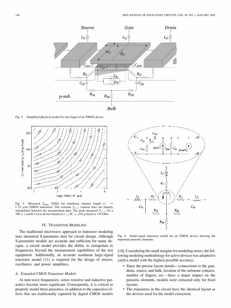
It can be shown theoretically that is independent of thenumber of fingers of a multi-finger transistor. Therefore, it issufficient to only consider the optimal layout for a single finger.The physical layout of a single finger is shown in Fig. 2, alongwith a physical model depicting the dominant high-frequencyloss mechanisms. As mentioned, is limited by resistivelosses, the most significant being the gate resistance , se-ries source/drain resistances , nonquasi-static channelresistance , and resistive substrate network ( , and
) [10].
Fig. 1. Measured (markers) and modeled (solid lines) unilateral gain U ,maximum stable gain MSG, maximum available gain MAG, and currentgain h , for a typical NMOS device (W=L = 100 � 1 �m/0.13 �m,I =W = 300 �A/�m, V = 1:2 V). The maximum frequency ofoscillation, based upon the device circuit model, is f = 135 GHz. Thisis much lower than the value of 200 GHz attained if a 20-dB/decade slope isassumed.
By using narrow finger widths, the effect of the gate resis-tance can be made negligible compared to the other parasiticsresistors. The polysilicon gate sheet resistance only affectshow narrow the fingers must be made. Therefore, with optimallayout, is not limited by the gate resistance, but is pri-marily determined by the series source/drain resistances andsubstrate losses.
C. Measured
The optimal transistor finger width for our 130-nm digitalCMOS process has been determined empirically. The measured
for NMOS transistors with minimum channel length as afunction of finger width and bias current density is displayed inFig. 3. Nine devices with – m and –in common-source configuration with the bulk and sourcegrounded and the gate contacted on one side were fabricated.For six bias points ( – A/ m) per device,a transistor model was extracted from the measured data inorder to find (see Section IV). The constant con-tours shown in Fig. 3 were linearly interpolated between themeasured data points.
For a constant current density, the device remains fixed(e.g., A/ m, is 70 GHz). It is clear fromFig. 3 that, depending on the finger width, can be muchlarger or smaller than . Thus, the optimal layout for mm-waveapplications requires CMOS transistors to be designed usingmany extremely narrow fingers in parallel (less than 1 m each).This is in stark contrast to GaAs FETs with metal gates, whererelatively few fingers of wide devices ( – m) aretypically used [8]. Furthermore, the device must be biased wellinto strong inversion (around 100–300 A/ m) for mm-waveoperation. By proper layout and biasing, though, the of anNMOS transistor in a standard 130-nm CMOS technology caneasily surpass 100 GHz, opening the possibility for mm-wavecircuits.
146 IEEE JOURNAL OF SOLID-STATE CIRCUITS, VOL. 40, NO. 1, JANUARY 2005
Fig. 2. Simplified physical model for one finger of an NMOS device.
Fig. 3. Measured f [GHz] for minimum channel length (L =
0:13 �m) NMOS transistors. The constant f contour lines are linearlyinterpolated between the measurement data. The peak measured f for a100� 1 �m/0.13 �m device biased at I =W = 250 �A/�m is 135 GHz.
IV. TRANSISTOR MODELING
The traditional microwave approach to transistor modelinguses measured S-parameter data for circuit design. AlthoughS-parameter models are accurate and sufficient for many de-signs, a circuit model provides the ability to extrapolate tofrequencies beyond the measurement capabilities of the testequipment. Additionally, an accurate nonlinear large-signaltransistor model [11] is required for the design of mixers,oscillators, and power amplifiers.
A. Extended CMOS Transistor Models
At mm-wave frequencies, series resistive and inductive par-asitics become more significant. Consequently, it is critical toproperly model these parasitics, in addition to the capacitive ef-fects that are traditionally captured by digital CMOS models
Fig. 4. Small-signal transistor model for an NMOS device showing theimportant parasitic elements.
[10]. Considering the small margins for modeling errors, the fol-lowing modeling methodology for active devices was adopted toyield a model with the highest possible accuracy:
• Since the precise layout details—connections to the gate,drain, source, and bulk, location of the substrate contacts,number of fingers, etc.—have a major impact on theparasitic elements, models were extracted only for fixedlayouts.
• The transistors in the circuit have the identical layout asthe devices used for the model extraction.

DOAN et al.: MILLIMETER-WAVE CMOS DESIGN 147
Fig. 5. Measured (markers) and simulated (solid lines) S-parameters for a typical NMOS device (W=L = 100 � 1 �m/0.13 �m, I =W = 300 �A/�m,V = 1:2 V).
• For the highest accuracy, a bias-dependent small-signalmodel is extracted. For increased flexibility, a large-signaltransistor model based on BSIM3 has also been demon-strated to provide good results up to 65 GHz [11].
The physical model depicting the significant high-fre-quency parasitics was shown in Fig. 2, and Fig. 4 shows thecorresponding extended circuit model. The core device ismodeled using either a lumped small-signal model (Fig. 4)or using a standard BSIM3 model card. In addition to theparasitic resistors, series inductors must be added to allterminals— —to properly model the delay effectsassociated with interconnect wiring. Notice that all of the ca-pacitors (e.g., ) account for both the traditionally“intrinsic” channel and overlap capacitances as well as thetraditionally “extrinsic” wiring capacitances.
For each model, the extrinsic component values and deviceparameters were extracted from measured data using a hybrid
optimization algorithm in Agilent IC-CAP [19]. S-parametersfor the simulated small-signal model and measured data up to65 GHz are shown in Fig. 5 for a 100 1 m/0.13 m NMOStransistor biased at V and V. Theexcellent broadband accuracy of the simulation compared to themeasured data verifies that the topology of our model is correctand complete. Furthermore, it also demonstrates that distributedeffects and frequency-dependent losses caused by the skin effectcan be adequately accounted for using only lumped extrinsiccomponents with frequency-independent values. Large-signalverification has also been performed on the BSIM3 model [11],showing good distortion prediction at mm-wave frequencies.The default BSIM3 noise model was used since no devicenoise measurements were available.
The transistor gains—Mason’s unilateral gain, maximumstable gain (MSG), maximum available gain (MAG), andcurrent gain—for this device are plotted in Fig. 1. The accurate

148 IEEE JOURNAL OF SOLID-STATE CIRCUITS, VOL. 40, NO. 1, JANUARY 2005
Fig. 6. Distributed RLGC lossy transmission line model.
modeling of the unilateral gain is particularly important. Unlikethe MSG and current gain, Mason’s unilateral gain is a verystrong function of all resistive losses. Therefore, accuratelyfitting the unilateral gain validates that the important loss mech-anisms have been properly modeled. As mentioned earlier,these resistive losses are critical because they ultimately limitthe high-frequency capabilities of the transistor.
V. TRANSMISSION LINES
Transmission lines (T-lines) are important structures formm-wave design. At these frequencies, the reactive elementsneeded for matching networks and resonators become in-creasingly small, requiring inductance values on the orderof 50–250 pH. Given the quasi-transverse electromagnetic(quasi-TEM) mode of propagation, T-lines are inherentlyscalable in length and are capable of realizing precise valuesof small reactances. Additionally, interconnect wiring can bemodeled directly when implemented using T-lines. Anotherbenefit of using T-lines is that the well-defined ground returnpath significantly reduces magnetic and electric field couplingto adjacent structures.
Any quasi-TEM T-line can be completely characterized byits equivalent frequency-dependent RLGC distributed circuitmodel (Fig. 6). The line can also be characterized by thefollowing four real parameters:
(1)
(2)
(3)
(4)
Unlike T-lines implemented on GaAs, where is essentiallyzero, T-lines implemented on low-resistivity silicon often havelow capacitive quality factors due to the substrate cou-pling. For T-lines that store mostly magnetic energy, the in-ductive quality factor is the most critical parameter whendetermining the loss of the line, as opposed to the resonatorquality factor or the attenuation constant.
A. Inductive Quality Factor
Transmission lines are often used to resonate with theintrinsic capacitance of the transistors (e.g., when used inmatching networks). In this case, the line stores mostly mag-netic energy, and it is therefore most appropriate to considerthe power lost for a given amount of net reactive energy stored
in the line, as opposed to the total stored energy [13]. Thus, formatching networks, the most meaningful metric is
(5)
where is the resonance frequency, and are the av-erage magnetic and electric energy stored, and and arethe average power dissipated in the resistance and conductance,respectively. If and are rewritten as
(6)
(7)
it is straightforward to show that
(8)
where
(9)
(10)
If the line is inductive (i.e., ), then ,and . The loss in the line is therefore almostcompletely determined by . For example, consider a shortedtransmission line with . In this case, it can be shownthat , which greatly reduces the impact of the shuntlosses on the inductive line. This is particularly important forintegrated T-lines on silicon, where the low-resistivity substratecauses to be nonnegligible. A similar qualitative discussionand conclusion for inductive lines has been presented in [14].
B. Microstrip Versus Coplanar Waveguides
Microstrip lines on silicon are typically implemented usingthe top-layer metal as the signal line, and the bottom-layer metalfor the ground plane. Fig. 7(a) illustrates the effectiveness of themetal shield, with essentially no electric field penetration intothe substrate. The shunt loss, , is therefore due only to theloss tangent of the oxide, yielding a capacitive quality factor,
, of around 30 at mm-wave frequencies [Fig. 8(b)]. Thebiggest drawback to microstrip lines on standard CMOS is theclose proximity of the ground plane to the signal line ( m),yielding very small distributed inductance, . This significantlydegrades the inductive quality factor, [Fig. 8(a)].
Another option for on-chip transmission lines is the useof coplanar waveguides (CPWs) [16], [17], which are im-plemented with one signal line surrounded by two adjacentgrounds [Fig. 7(b)]. The signal width, , can be used tominimize conductor loss, while the signal-to-ground spacing,
, controls the and the tradeoff between , and . Asan example, a CPW with m and m has a
of 59 and a measured to be about double that of themicrostrip [Fig. 8(a)]. Therefore, CPW T-lines were used inour designs due to their considerably higher compared tomicrostrip lines.

DOAN et al.: MILLIMETER-WAVE CMOS DESIGN 149
Fig. 7. Electric field distributions from 3-D EM simulations of (a) microstrip and (b) coplanar waveguide transmission lines.
By varying the signal-to-ground spacing, it is possible to de-sign CPW lines to have either large and high-impedance( m) or large and low-impedance ( m)(Fig. 9). On the other hand microstrip lines have, to first-order,constant and regardless of geometry. Another importantissue when designing with CPWs is the unwanted odd CPWmode, which arises because CPW lines inherently have threeconductors. To suppress this parasitic propagation mode, thetwo grounds should be forced to the same potential [16]. InMMICs, this requires the availability of air bridge technology,which is costly and not supported by all foundries. Underpassesusing a lower metal level in a modern CMOS process can beused to suppress this mode.
VI. TRANSMISSION LINE MODELING
To achieve the highest level of accuracy for the transmissionline models, a design-oriented modeling methodology, similarto [18], has been chosen for this work. The modeling approachis based on measured transmission line data and the modelsare optimized to fit most accurately at mm-wave frequencies.Scalable (in length) electrical models, which capture the high-level behavior of the lines, have been used and are supported
in most simulators such as SpectreRF, ADS, and Eldo. Themodel parameters are easy to obtain from measured data orphysical EM simulations since only a relatively small numberof parameters are required to model the broadband performanceof each transmission line: characteristic impedance, effectivedielectric constant, attenuation constant, and loss tangent. Afirst-order frequency-dependent loss model is used. The modelassumes that the conductor loss is only caused by the skineffect losses, and the shunt loss is due to a constant losstangent. From Figs. 8 and 9, it can be seen that the lossesare well-modeled.
Using simple electrical models has many advantages. Thesimulation time is very fast, and the models can be easily inte-grated into circuit simulators and optimizers. The T-line modelsassume no coupling to adjacent structures. This assumption isjustified as the well-defined ground return path, which helpsconfine the magnetic and electric fields, and the close proximityof the adjacent grounds to the signal line help to minimize anysecond-order effects.
A CMOS test chip was fabricated which included 1-mm longCPW and microstrip transmission lines of different cross-sec-tional dimensions. A different transmission line model was ex-tracted for each geometry. Notice that although the overall loss

150 IEEE JOURNAL OF SOLID-STATE CIRCUITS, VOL. 40, NO. 1, JANUARY 2005
Fig. 8. Measured (markers) Q and Q for a coplanar waveguide and amicrostrip line. The solid lines are for an empirical first-order model where theR variation is due only to skin effect and G is caused by a constant dielectricloss tangent.
of the T-line can be accurately extracted from measurements,decomposing this loss into individual loss components causesthe measured high- data (e.g., for microstrip) to exhibitmore measurement uncertainty than the low- data.
VII. COPLANAR WAVEGUIDE FILTER
To validate the electrical passive models, a 30-GHz bandpassfilter, composed of series and shunt stubs of the modeled CPWlines, was designed (Fig. 10). The topology of the filter is equiv-alent to a bandpass ladder filter. The shunt resonator is replacedby an open-circuited low-impedance line and a short-circuitedhigh-impedance line. The series transmission line in the centerreplaces the series resonator. Note that all lines are much shorterthan a wavelength ( mm on SiO ) to minimize loss. Pad
Fig. 9. Measured (markers)Q andQ for coplanar waveguides with varyinggeometries. The solid lines are for an empirical first-order model where the Rvariation is due only to skin effect andG is caused by a constant dielectric losstangent.
models were also extracted from a test chip, and the pads wereincluded as part of the filter. An optimizer was used to fine tunethe line lengths.
A die photo of the filter is shown in Fig. 11, measuring0.93 mm 0.64 mm including pads. Although the transmissionlines meander, no special modeling of the bends or junctionswas performed. The measured and simulated results for the30-GHz filter are plotted in Fig. 12, demonstrating excellentbroadband agreement by using just the simple, scalable elec-trical models. The measured insertion loss is 2 dB, and the inputand output return losses are better than 25 dB. The accurateprediction by the electrical models demonstrates that junctionsand bends are not critical, and verifies that there is no significantcoupling between the individual lines.

DOAN et al.: MILLIMETER-WAVE CMOS DESIGN 151
Fig. 10. Schematic of the 30-GHz CPW filter.
Fig. 11. Chip microphotograph of the 30-GHz CPW filter.
VIII. AMPLIFIER DESIGN
Two wideband mm-wave amplifiers designed as general-pur-pose amplifiers operating at 40 GHz and 60 GHz have beenfabricated in a 130-nm digital CMOS technology with nospecial analog or RF options. Figs. 13 and 14 show the diemicrophotograph of the 40-GHz amplifier, which measures1.3 mm 1.1 mm including pads, and the 60-GHz amplifier,which measures 1.3 mm 1.0 mm including pads.
Both amplifiers were designed to have about 25% bandwidth.The topology of the two amplifiers is essentially identical, con-sisting of three stages of cascode devices with input, output, andinterstage reactive matching (Fig. 15). The only significant dif-ferences between the two amplifiers are the bias currents andlengths of the transmission lines.
Cascode transistors are used in order to reduce the Miller ca-pacitance and improve stability, and are unconditionally stableabove 27 GHz. The cascode transistors for the 40 GHz amplifierare biased at a current density of 100 A/ m, with a MAG of8.9 dB at 40 GHz. For the 60-GHz amplifier, the cascodes arebiased at 150 A/ m, and the MAG is 6.0 dB at 60 GHz. Thedevices are biased from a of 1.5 V for increased headroomand output power. From simulations, all terminal-pair voltagesfor the individual transistors remain below the rated breakdownvoltages.
Fig. 12. Measured and simulated results for the 30-GHz CPW filter.
Fig. 13. Chip microphotograph of the 3-stage 40-GHz CPW amplifier.
CPW transmission lines are used extensively in the designfor impedance matching, interconnect wiring, and the bias net-works. All lines are kept as short as possible to minimize lossesand are significantly shorter than ( m for the 40-GHzamplifier, m for the 60-GHz amplifier). The T-lines atthe gate and drain are used to supply bias and are also incor-porated into the matching networks. Meander CPW lines areused throughout the 40-GHz design in order to reduce area. Theinsertion loss of the interstage matching network is 2.5 dB forthe 40-GHz design and 1.8 dB for the 60-GHz amplifier. In-terestingly, the losses due to the passives are lower at 60 GHz.Although the conductor loss due to skin effect increases withfrequency, the lines needed for the matching networks becomeshorter.
The input and output of the amplifiers are ac-coupled, andthe GSG pads are included as part of the design. Both ports aredesigned to be matched to 50 . The insertion loss of the inputmatching network is 1.6 dB and 1.3 dB, and the insertion loss

152 IEEE JOURNAL OF SOLID-STATE CIRCUITS, VOL. 40, NO. 1, JANUARY 2005
Fig. 14. Chip microphotograph of the 3-stage 60-GHz CPW amplifier.
Fig. 15. Simplified schematic of the 60-GHz 3-stage amplifier using CPWtransmission lines.
of the output matching network is 2.0 dB and 1.6 dB for the40-GHz and 60-GHz amplifiers, respectively.
IX. MEASUREMENT RESULTS
A. Measurement Setup
On-wafer S-parameter measurements up to 65 GHz were per-formed using a Cascade Microtech probe station, GSG coplanarprobes, and an Anritsu 37 397C VNA. Open-short de-embed-ding [12] was used to remove the effects of the pads when mea-suring individual devices (transistors, transmission lines, etc.).Pad removal was not necessary for the filter or amplifiers sincethe pads were incorporated into the design.
The VNA was also used for single-tone compression mea-surements up to 65 GHz. A 65-GHz Anritsu SC6230 powersensor and Anritsu 2437A power meter was used to calibrateout the losses of the cabling and probes.
On-wafer vector-corrected two-tone distortion measure-ments were performed on a custom setup using the proceduredescribed in [20]. The measurement system was limited to50 GHz, so the intermodulation distortion was characterizedonly for the 40-GHz amplifier. A reflectometer external to theVNA was mounted on the probe station to maximize dynamicrange. Both on-wafer and coaxial calibration standards areneeded to obtain the vector-corrected power at the probe tip. Afull description of the procedure and algorithm for de-embed-ding can be found in [20].
Fig. 16. Measured (markers) and simulated (lines) S-parameters for the40-GHz amplifier.
Fig. 17. Measured two-tone (38 GHz and 38.25 GHz) distortion for the40-GHz amplifier.
Noise figure (NF) measurement of the 60-GHz amplifier wasperformed using a Millitech WR-15 noise source, WR-15 wave-guide probes, output isolator, OML 50–75-GHz DSB down-conversion mixer, and an Agilent N8973A NF measurementsystem.
B. 40-GHz and 60-GHz Amplifier Results
The measured and modeled S-parameters for the 40-GHzamplifier are shown in Fig. 16. The amplifier achieves a peakpower gain of 19 dB, and input and output return losses are
dB. The 3-dB bandwidth is 34–44 GHz, and the amplifiermaintains good return losses across this band. The measuredreverse isolation is better than 50 dB up to 65 GHz, indicatingthat parasitic coupling through the silicon substrate is very small.This isolation is obtained without any special isolation strategysuch as triple-well. The two-tone intermodulation distortion

DOAN et al.: MILLIMETER-WAVE CMOS DESIGN 153
Fig. 18. Measured (markers) and simulated (lines) S-parameters for the60-GHz amplifier.
Fig. 19. Measured output 1-dB compression point for the 60-GHz amplifier.
measurements are shown in Fig. 17. The measured output1-dB compression point is dBm and IIP3 is
dBm. Simulations predict an output of dBmand IIP3 of dBm. The noise figure of this amplifier hasnot been measured, but the simulations show a NF of 5.4 dB.This amplifier dissipates 24 mA from a 1.5-V supply.
The 60-GHz amplifier has also been characterized, and theS-parameters are shown in Fig. 18. The amplifier achievesa peak power gain of 12 dB, input and output return losses
dB, and the 3-dB bandwidth is 51–65 GHz. The mea-sured reverse isolation is better than 45 dB up to 65 GHz.The measured output over frequency is given in Fig. 19.The frequency range is limited by the ability for the VNA todrive the amplifier into saturation. At 60 GHz, the measuredoutput is dBm, while simulations predict output
Fig. 20. Measured noise figure and gain for the 60-GHz amplifier.
TABLE ICOMPARISON WITH STATE-OF-THE-ART BULK-CMOS AMPLIFIERS
of dBm and IIP3 of dBm. The output powerof the 60-GHz amplifier is higher than the 40-GHz amplifierprimarily because of the extra bias current. If the efficiency iskept constant, increasing the current by 50% results in a 3.5 dBincrease in output power.
The measured NF of the 60-GHz amplifier is shown inFig. 20. No de-embedding of any on-chip losses was performedsince the pads and input match were part of the design. The NFis 8.8 dB at 60 GHz and remains below 9.3 dB up to 63 GHz.This is higher than the 6.9 dB predicted by simulations becausethe default BSIM3 noise model that was used does not properlyaccount for effects such as excess short-channel thermal noiseor induced gate noise. A more advanced RF transistor model,such as BSIM4 or MOS11, would be required to accuratelypredict the noise performance. This amplifier dissipates 36 mAfrom a 1.5-V supply. A summary of the measured results isprovided in Table I along with a comparison to state-of-the-artbulk-CMOS amplifiers.

154 IEEE JOURNAL OF SOLID-STATE CIRCUITS, VOL. 40, NO. 1, JANUARY 2005
X. CONCLUSION
A mm-wave design and modeling methodology for CMOSdevices and circuits has been presented. Optimization of theactive and passive components for mm-wave circuits leads totransistors with finger widths m and the use of CPW trans-mission lines. A modeling methodology, using relatively simplemodels that carefully account for the resistive losses, has beendescribed and applied to transistors and transmission lines. Themodels have been verified to achieve broadband accuracy fromdc to 65 GHz. Finally, two wideband mm-wave CMOS ampli-fiers, operating at 40 GHz and 60 GHz, were fabricated usinga 130-nm bulk-CMOS technology. The measured S-parameterscorrespond extremely well to the simulated models owing tothe accurate device modeling. The 40-GHz amplifier achieves19-dB gain, output dBm, and dBm,while consuming 36 mW. The 60-GHz amplifier achieves 12-dBgain, output dBm, and dB, whileconsuming 54 mW. These are the first demonstrated amplifiersoperating above 30 GHz fabricated using a mainstream bulk-CMOS technology. These amplifiers greatly improve on the cur-rent state-of-the-art, owing to the mm-wave CMOS design andmodeling approach described in this work.
ACKNOWLEDGMENT
The authors acknowledge STMicroelectronics and B. Guptafor chip fabrication. The authors thank A. Cognata andT. Shirley of Agilent Technologies, Santa Rosa, for helpwith two-tone and distortion measurements, and H. Tran andK. Fujii of Agilent Technologies, San Jose, for help with noisefigure measurements. Useful discussions and feedback fromG. Baldwin, A. Vladimirescu, D. Yee, I. O’Donnell, J. Vander-haegen, J. Weldon, and the BWRC OGRE group were greatlyappreciated.
REFERENCES
[1] L. M. Franca-Neto, R. E. Bishop, and B. A. Bloechel, “64 GHz and100 GHz VCO’s in 90 nm CMOS using optimum pumping method,” inIEEE Int. Solid-State Circuits Conf. Dig. Tech. Papers, Feb. 2004, pp.444–445.
[2] R.-C. Liu, H.-Y. Chang, C.-H. Wang, and H. Wang, “A 63 GHz VCOusing a standard 0.25 �m CMOS process,” in IEEE Int. Solid-State Cir-cuits Conf. Dig. Tech. Papers, Feb. 2004, pp. 446–447.
[3] M. Tiebout, H.-D. Wohlmuth, and W. Simbürger, “A 1 V 51 GHz fully-integrated VCO in 0.12 �m CMOS,” in IEEE Int. Solid-State CircuitsConf. Dig. Tech. Papers, Feb. 2002, pp. 238–239.
[4] K.-W. Yu, Y.-L. Lu, D.-C. Chang, V. Liang, and M. F. Chang, “K-bandlow-noise amplifiers using 0.18 �m CMOS technology,” IEEE Microw.Wireless Compon. Lett., vol. 14, no. 3, pp. 106–108, Mar. 2004.
[5] L. M. Franca-Neto, B. A. Bloechel, and K. Soumyanath, “17 GHzand 24 GHz LNA designs based on extended-S-parameter with mi-crostrip-on-die in 0.18 �m logic CMOS technology,” in Proc. Eur.Solid-State Circuits Conf., Sep. 2003, pp. 149–152.
[6] X. Guan and A. Hajimiri, “A 24 GHz CMOS front-end,” in Proc. Eur.Solid-State Circuits Conf., Sep. 2002, pp. 155–158.
[7] M. Madihian, H. Fujii, H. Yoshida, H. Suzuki, and T. Yamazaki, “A 1–10GHz, 0.18 �m-CMOS chipset for multi-mode wireless applications,” inIEEE MTT-S Int. Microwave Symp. Dig., June 2001, pp. 1865–1868.
[8] I. Bahl and P. Bhartia, Microwave Solid State Circuit Design, 2nded. Hoboken, NJ: Wiley, 2003.
[9] R. Spence, Linear Active Networks, London: Wiley, 1970.[10] C. Enz, “An MOS transistor model for RF IC design valid in all regions
of operation,” IEEE Trans. Microw. Theory Tech., vol. 50, no. 1, pp.342–359, Jan. 2002.
[11] S. Emami, C. H. Doan, A. M. Niknejad, and R. W. Brodersen, “Large-signal millimeter-wave CMOS modeling with BSIM3,” in IEEE RFICSymp. Dig., Jun. 2004, pp. 163–166.
[12] M. C. A. M. Koolen, J. A. M. Geelen, and M. P. J. G. Versleijen, “Animproved de-embedding technique for on-wafer high-frequency char-acterization,” in Proc. IEEE Bipolar/BiCMOS Circuits and TechnologyMeeting, Sep. 1991, pp. 188–191.
[13] C. P. Yue and S. S. Wong, “On-chip spiral inductors with patternedground shields for Si-based RF IC’s,” IEEE J. Solid-State Circuits, vol.33, no. 5, pp. 743–752, May 1998.
[14] F. Ellinger, “26–42 GHz SOI CMOS low noise amplifier,” IEEE J. Solid-State Circuits, vol. 39, no. 3, pp. 522–528, Mar. 2004.
[15] S. Ramo, J. R. Whinnery, and T. Van Duzer, Fields and Waves in Com-munication Electronics, 3rd ed. New York: Wiley, 1994.
[16] T. C. Edwards and M. B. Steer, Foundations of Interconnect and Mi-crostrip Design, 3rd ed. New York: Wiley, 2000.
[17] B. Kleveland, C. H. Diaz, D. Vook, L. Madden, T. H. Lee, and S. S.Wong, “Exploiting CMOS reverse interconnect scaling in multigiga-hertz amplifier and oscillator design,” IEEE J. Solid-State Circuits, vol.36, no. 10, pp. 1480–1488, Oct. 2001.
[18] G. Carchon, W. De Raedt, and B. Nauwelaers, “Novel approach for adesign-oriented measurement-based fully scalable coplanar waveguidetransmission line model,” in IEE Proc. Microwave, Antennas Propagat.,vol. 148, Aug. 2001, pp. 227–232.
[19] Agilent IC-CAP 2002 User’s Guide [Online]. Available: http://eesof.tm.agilent.com
[20] B. Hughes, A. Ferrero, and A. Cognata, “Accurate on-wafer power andharmonic measurements of mm-wave amplifiers and devices,” in IEEEMTT-S Int. Microwave Symp. Dig., Jun. 1992, pp. 1019–1022.
Chinh H. Doan (S’99) received the B.S. degree fromthe California Institute of Technology, Pasadena, in1997, and the M.S. degree from the University ofCalifornia, Berkeley, in 2000, both in electrical en-gineering. He is currently working toward the Ph.D.degree at the University of California, Berkeley,where he is a member of the Berkeley WirelessResearch Center.
He held an internship position at Agilent Tech-nologies, in 2002, where he designed and fabricatedbroadband monolithic microwave integrated circuit
(MMIC) power amplifiers for test and measurement equipment operating upto 50 GHz using GaAs pHEMT technology. His current area of research isfocused on the design of millimeter-wave transceiver circuits on CMOS, activeand passive device modeling, and de-embedding and verification techniquesfor on-wafer probing on lossy substrates.
Sohrab Emami received the B.S. degree from theSharif University of Technology, Tehran, Iran, in1995, and the M.S. degree from the Tokyo Institute ofTechnology, in 2001, both in electrical engineering.He is currently working toward the Ph.D. degree atthe University of California, Berkeley, where he is amember of the Berkeley Wireless Research Center.
His current research is focused on the design, mod-eling, and analysis of CMOS frequency-convertingblocks such as mixers, frequency multipliers, and di-viders, for 60-GHz wireless systems. From 1995 to
1998, he co-founded KARA-Systems Inc. working on control and instrumenta-tion in the Iranian oil and natural gas industries. From 2000 to 2001, he held apart-time position at Hitachi Ltd., Tokyo, Japan, designing low-power CMOSbaseband filters for direct-conversion wideband-CDMA receivers. In 2003, hewas awarded the Hitachi-UC Berkeley Management of Technology Fellowship,where his responsibilities included the design and implementation of a multi-an-tenna prototype reader for the Hitachi MuChip RFID.
Mr. Emami also participated in the 21st International Physics Olympiad,Netherlands, and was the Gold Medal winner of the National Physics Olympiad.

DOAN et al.: MILLIMETER-WAVE CMOS DESIGN 155
Ali M. Niknejad (S’93–M’00) received the B.S.E.E.degree from the University of California, Los An-geles, in 1994, and the M.S. and Ph.D. degrees inelectrical engineering from the University of Cali-fornia, Berkeley, in 1997 and 2000, respectively.
From 2000 to 2002, he was with Silicon Labo-ratories, Austin, TX, where he was involved withthe design and research of CMOS RF integratedcircuits and devices for wireless communicationapplications. Presently, he is an Assistant Professorwith the Electrical Engineering and Computer Sci-
ence Department, University of California, Berkeley. He is an active memberat the Berkeley Wireless Research Center (BWRC) and he is the Codirectorof the BSIM Research Group. His current research interests lie within thearea of analog integrated circuits, particularly as applied to wireless andbroadband communication circuits. His interests also include device modelingand numerical techniques in electromagnetics.
Dr. Niknejad is currently serving as an Associate Editor of the IEEE JOURNAL
OF SOLID-STATE CIRCUITS.
Robert W. Brodersen (M’76–SM’81–F’82) re-ceived the Ph.D. degree from the MassachusettsInstitute of Technology, Cambridge, in 1972.
He was then with the Central Research Laboratoryat Texas Instruments for three years. Following that,he joined the Electrical Engineering and ComputerScience faculty of the University of California atBerkeley, where he is now the John Whinnery ChairProfessor and Co-Scientific Director of the BerkeleyWireless Research Center. His research is focusedin the areas of low-power design and wireless
communications and the CAD tools necessary to support these activities.Prof. Brodersen has won best paper awards for a number of journal and con-
ference papers in the areas of integrated circuit design, CAD, and communica-tions, including in 1979 the W.G. Baker Award. In 1983, he was co-recipient ofthe IEEE Morris Liebmann Award. In 1986, he received the Technical Achieve-ment Awards in the IEEE Circuits and Systems Society and in 1991 from theSignal Processing Society. In 1988, he was elected to be member of the NationalAcademy of Engineering. In 1996, he received the IEEE Solid-State CircuitsSociety Award and in 1999 received an honorary doctorate from the Universityof Lund in Sweden. In 2000, he received a Millennium Award from the Cir-cuits and Systems Society, the Golden Jubilee Award from the IEEE. In 2001he was awarded the Lewis Winner Award for outstanding paper at the IEEE In-ternational Solid-State Circuits Conference and in 2003 was given an award forbeing one of the top ten contributors over the 50 years of that conference.


![Time Table-Spring2011-RoomWise-[minor changes]](https://img.pdfslide.us/doc/110x75/577d2ea11a28ab4e1eaf9294/time-table-spring2011-roomwise-minor-changes.jpg)