Embed Size (px)
Citation preview
112 IEEE TRANSACTIONS ON INSTRUMENTATION AND MEASUREMENT, VOL. 25, NO. 2, JUNE 1976
A Versatile Pseudo-Random Noise Generator
E D W A R D D. L I P S O N , K E N N E T H W. F O S T E R , AND M I C H A E L P . W A L S H
Abstract—A detailed design is presented for a digital pseudo-random noise generator. The instrument is built with standard integrated circuits. It produces both binary noise (pseudo-ran-dom binary sequences) and white Gaussian noise of variable bandwidth. By setting front panel switches to match tabulated octal codes, one may select a vast number of independent noise programs.
INTRODUCTION
RA N D O M N O I S E is widely and increasingly used as a signal for the test ing and identification of physi-
cal and biological systems. In par t icular white Gaussian noise is becoming popular for the de te rmina t ion of t h e Wiener kernels [1], [2] of nonl inear biological sys tems [3]-[5].
Physical devices such as resistors a n d diodes are sometimes used as sources of r andom noise. However such devices suffer from stat ist ical variabil i ty between finite samples of their noise ou tpu t . Moreover unless special procedures are unde r t aken [6] physical noise sources are generally unsui table for low-frequency ap-plications.
Often it is adequa te , or even advantageous , t o employ determinis t ic (and reproducible) periodic signals with the essential stat ist ical proper t ies of r andom noise. Such pseudo- random noise may be genera ted by com-puters , or by electronic ins t rument s such as t h a t de-scribed here.
BACKGROUND ON P S E U D O - R A N D O M SIGNALS
Pseudo- random binary sequences ( P R B S ; also known as maximal length binary sequences, b inary m-se-quences, and chain codes) are genera ted in pract ice by a feedback shift register [7], [8]. In such a device the nex t inpu t value (bit) is de te rmined as follows. A par i ty check (or mod-2 addi t ion, or EXCLUSIVE-OR operat ion) is performed on the values in a fixed subse t of the stages of the shift register. T h e resul t is fed back to t he input .
If the feedback length (i.e., h ighest order feedback stage) of the shift register is n, t hen the re are 2n possi-ble s ta tes of the feedback shift register as a whole. One special s ta te , namely all zeros, is disallowed since it would be self-perpetuating. In general , t he remaining 2 n
— 1 s ta tes may be generated periodically in sequence in
Manuscript received December 29, 1975. This work was supported by the National Science Foundation under Grant BMS 70-00999 A04 to Prof. Max Delbrück.
E. D. Lipson and M. P. Walsh are with the Division of Biology, Cal-ifornia Institute of Technology, Pasadena, CA 91125.
Κ. W. Foster was with the Division of Biology, California Institute of Technology, Pasadena, CA. He is now with the Department of Mo-lecular, Cellular and Developmental Biology, University of Colorado, Boulder, CO 80302.
a n u m b e r of i ndependen t pa t t e rns . In such a case, t h e sequence of 2 n — 1 bi ts observed in any given stage con-s t i tu tes a maximal length or P R B S .
Only cer ta in feedback configurations produce P R B S ' s . In general , t he configuration of a feedback shift register may be represented algebraically by a polynomial over the Galois field with two e lements (GF(2)) [9]. For example , t he polynomial X 8 + X 4 + X 3
+ X2 + 1 represents a shift register with feedback from stages 2, 3, 4, and 8. T h e degree of t he polynomial , here 8, is equivalent to t he feedback length η of t he shift reg-ister. Those feedback configurations which produce P R B S ' s correspond to polynomials which are " i r reduci-b l e " and "p r imi t ive" [7]. Using a compact octal code, Pe te r son and Weldon [9] have t abu la t ed irreducible polynomials u p to degree 34. In thei r tabula t ion , only those polynomials with suffixes E, F, G, and Η are pr imit ive .
For t he example above the octal code is 435, corre-sponding to t he b inary code 100011101. T h e binary code in t u r n represen ts t he above polynomial , wr i t ten explic-itly as 1-X 8 + 0 -X 7 + 0 -X 6 + 0 - X 5 + 1-X 4 + 1-X 3 + 1-X 2
+ 0-X 1 4- 1-X°. No te t h a t in t he shift register, the re is no stage corresponding to t he zero-order te rm.
On t h e front panel of t he in s t rumen t described here , t h e opera tor may dial in an octal code of u p to seven digits to produce any feedback configuration with feed-back length η < 20. T h u s , in par t icular , one may gener-a te easily t he P R B S for every allowed octal code u p to degree 20. A row of 20 lamps is available to display ei-the r t h e b inary feedback code or t he last 20 values of t he ongoing P R B S . By means of a special synchroniza-t ion signal (sync), described later, one may de te rmine whe ther or no t any given octal code produces a P R B S .
P R B S ' s have a n u m b e r of proper t ies which qualify t h e m as subs t i tu tes for r a n d o m binary signals [7]. T h e proper t ies include (periodic) impulse-l ike autocorrela-t ion functions, equal i ty of t he n u m b e r of occurrences of t h e high and low s ta tes (actually the re is an excess of one high), and an exponential ly decreasing d is t r ibut ion of lengths of consecutive runs of high (or low) s ta tes .
T h e power spec t rum of a P R B S with a clock interval At (for t he shift register) is a line spec t rum, because of t he periodici ty of the P R B S . T h e harmonic separa t ion of t he lines is Δ / = 1/NAt. T h e envelope of t he line spec t rum is propor t ional to sine 2f(t) [10]. [Note: sine (X) = sin ( π Χ ) / ( 7 τ Χ ) . ] T h u s t h e spec t rum is approxi-mate ly flat (within 3 dB) u p to / = 1/3 At.
By means of filtering, P R B S ' s m a y be e laborated into pseudo- random waveforms with a var ie ty of s tat is t ical a n d spectral proper t ies . Analog low-pass filtering pro-

LIPSON et ai: PSEUDO-RANDOM NOISE GENERATOR 113
duces cont inuous waveforms. Digital filtering produces multilevel s tep waveforms, which may approx imate con-t inuous waveforms. Analog filtering suffers from a n u m -ber of disadvantages . If one changes t h e clock interval Δί, t he characteris t ics of t he analog filter m u s t be modi -fied, generally no t a s imple ma t t e r . Moreover, analog filters are unsui tab le for low^frequency appl icat ions , such as t he one in which t h e p resen t i n s t rumen t was used [5].
These disadvantages are overcome by digital filtering. T h e availability of t h e shift register as a digital delay line makes digital filtering very s imple [11]. One need only perform a weighted sum of t he con ten t s of t he shift register stages. T h e digital filter character is t ics scale automatical ly when the clock interval is changed, such t h a t the waveform remains unchanged in shape. T h e weighting function appl ied here to t h e 32-stage shift register is a t runca ted sine (X) function [10], [12]. T h i s choice approaches t he ideal of a rectangular low-pass filter. T h e resu l tan t band- l imi ted whi te Gauss ian noise is jus t of the form needed for nonl inear sys tem identifi-cation [2].
T h e ins t rumen t produces bo th pseudo- random bina-ry noise and pseudo- random band- l imi ted whi te Gauss-ian noise. I t is bui l t wi th T T L digital in tegra ted circuits, as well as passive componen t s and one integrated-cir-cuit operat ional amplifier. I t has been used to measure the Wiener kernels of t he l ight-growth response sys tem of Phy corny ces [5]. T h e low b a n d w i d t h of t h a t sys tem (2.5 X 10~ 3 Hz) called for a noise genera tor capable of operat ion a t very low frequency. T h e digital design of the in s t rumen t pe rmi t s opera t ion a t arbi t rar i ly low fre-quency.
CIRCUIT DESCRIPTION
T h e general s t ruc tu re of t h e noise genera tor is shown in Fig. 1. T h e hea r t of t he i n s t r u m e n t is t h e shift regis-ter shown in t he center . Given t h e p resen t shift register contents and an (allowed) octal code, t h e feedback gen-erator evaluates t h e nex t b i t of t he P R B S and delivers it to the inpu t stage of t h e shift register. In addi t ion , t h e feedback generator au tomat ica l ly s t a r t s t he P R B S after the shift register has been cleared. T o produce whi te Gaussian noise t he P R B S is processed by a digital low-pass filter, consisting of t h e shift register itself in para l -lel with a sui tably weighted digi tal- to-analog conver ter [12].
Assuming clock pulses are provided to t h e shift regis-ter, t he central pa thway of Fig. 1 produces bo th b inary and Gaussian noise signals. T h e remaining e lements are optional, depending on the appl icat ion. T h e lamps indi-cate ei ther the b inary represen ta t ion of t h e octal code (i.e., which stages are fed back) or t h e s ta tes of t h e first 20 stages of the shift register. T h e sync genera tor p ro-vides one pulse per period of t he P R B S . T h i s pape r will not provide detai led designs of t h e active filter, clock, counter , or display since these are all s t a n d a r d a n d should be tai lored to specific appl ica t ions .
OCTAL CODE
ISWITCHES
f
>
LAMP MULTI-
PLEXERS ι DRIVERS
feedback IgeneratorI
SYNC L x U GENERATOR f̂ J
ι 1 ! COUNTER ! I DISPLAY I L 1 BINARY SEQUENCE
SHIFT REGISTER to,
DIGITAL TO ANALOG ANALOG NOISE
ACTIVE 1 SMOOTHED ANALOG I • NOISE (OPTIONAL)
I FILTER ι I J
SYNC Fig. 1. Block diagram of noise generator. The dashed boxes are
optional.
OCTAL CODE S W I T C H E S LEAST SIGNIFICANT
DIGIT ι— -i 20 19 18
C20C,9 SHIFT REGISTER
F T r i * ' .
I SERIAL INPUT BINARY
" OUTPUT
Fig. 2. Showing numbering conventions for outputs of 7 binary-coded octal switches (Digitran 8608) and 32-bit shift register (4 X SN74164 8-bit parallel-out serial shift registers).
Fig. 2 defines t he signals a n d number ing conventions for t h e octal code, t h e shift register s tages a n d t h e indi-cator lamps . T h e shift register is cleared by pressing the m o m e n t a r y reset switch. Posi t ive clock pulses may be provided by an in te rna l or external clock. In addi t ion pulses m a y be appl ied by a switch to single s tep t he bi-nary sequence for tes t ing. T h e binary output (PRBS) is t aken from stage 1 of t he shift register.
T h e feedback genera tor is shown in Fig. 3. (In th is a n d t h e o ther circuit d iagram, positive logic conven-t ions are used.) According to t h e set t ings of t he octal code switches, a subse t of t he bi ts Cj will be high. T h e AND gates A enable t he corresponding shift register stages Si to be t es ted by t h e par i ty checker. T h e resul t is fed back to the serial i npu t (stage 1) of t h e shift regis-ter . T h e combina t ion of the NOR gates C and the NAND gate D, together equivalent to a 32- input OR, tes ts for t h e special case when all of t h e Sj are low. In th is case (when all d a t a inpu ts are low) the ODD and EVEN inputs to t he par i ty checker are set high and low, respectively. T h i s case does no t occur dur ing the normal generat ion of P R B S ' s . W i t h o u t th is feature, though, the instru-m e n t could get s tuck (e.g., a t t u r n on) with the shift-register in its all-zero s ta te . Moreover this feature has two appl icat ions . By simply clearing (resetting) the shift register, t h e shift register (and t h u s t he P R B S ) , regard-less of t h e octal code, is initialized (at the next clock pulse) to a s t anda rd s ta te with .Si high and all other Sj low. In add i t ion by simply set t ing t h e octal code switch-es all to zero, a single high s ta te may be circulated re-
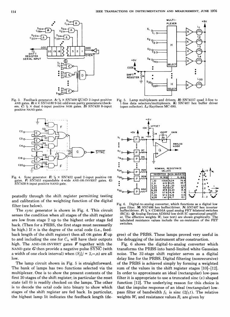
114 IEEE TRANSACTIONS ON INSTRUMENTATION AND MEASUREMENT, JUNE 1976
O D D
TO SHIFT
REGISTER
20 19 18 w 3 2 1
ν J EVEN
>32<
Fig. 3. Feedback generator. A: l/4 X SN7408 QUAD 2-input positive AND gates. B: 4 X SN74180 9-bit odd/even parity generators/check-ers. C: lk X dual 4-input positive NOR gates. D: SN7430 8-input positive NAND gate.
C| o -
S 2 ( C 2 O -
C 3 0 -
f 5 V S 4 O-
CODE
SHIFT REGISTER TER γ
C 4 0 -
C20O-
MULTI-PLEXER
SELECT!
H
SELECT!
5V
L, k
L 2 0
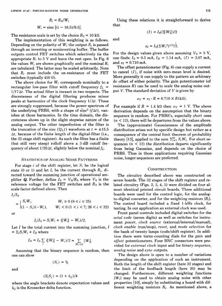
Fig. 5. Lamp multiplexers and drivers. H: SN74157 quad 2-line to 1-line data selectors/multiplexers. K: SN7407 hex buffer driver (open collector). LJ: Raytheon MC-680.
S Y N C
Fig. 4. Sync generator. Ε: \ X SN7432 quad 2-input positive OR gates. F: SN7453 expandable 4-wide AND-OR-INVERT gates. G: SN7430 8-input positive NAND gate.
peatedly through the shift register permi t t ing tes t ing and calibration of the weighting function of the digital filter (see below).
T h e sync generator is shown in Fig. 4. Th i s circuit senses the condit ion when all stages of t he shift register are low from stage 2 up to the highest order stage fed back. (Then for a P R B S , the first stage m u s t necessarily be high.) If η is the degree of the octal code (i.e., feed-back length of the shift register) t hen all OR gates Ε u p to and including the one for Cn will have their ou tpu t s high. T h e AND-OR-INVERT gates F together with t he NAND gate G t hen provide a negative pulse SYNC (with a width of one clock interval) when (Sj\j = 2,—,n) are all low.
T h e l amp circuit shown in Fig. 5 is s t raightforward. T h e bank of lamps has two functions selected via t he mult iplexer. One is to show the presen t contents of t he first 20 stages of the shift register; in par t icular the reset s ta te (all 0) is readily checked on the lamps . T h e o ther is to decode the octal code into b inary to show which stages of the shift register are fed back. In par t icular , t he highest l amp lit indicates the feedback length (de-
I 0 0 P F GAIN
o—E>>-{P
o — Ρ
ο — | ϊ > - Ρ
R 2 4
R 2 6 k / w 4
2 o—£*>- |p
N O M I N A L R E S I S T A N C E V A L U E S
I N V E R T E D NON-INVERTED
i R i (KÛ) i Ri (KÛ)
1,32 108.8 2,31 672 3 ,30 51,9 4,29 46.4 5,28 47.5 6,27 57.6 7,26 97.2 8,25 ( » )
9,24 76.8 10,23 35.7 11,22 22.7 12,21 16.7 13,20 13.4 14,19 11.6 15,18 10.5 16,17 10.1
° f
. 6 ·
.4 *
2 · 2 %S
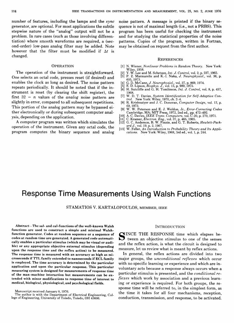
Fig. 6. Digital-to-analog converter, which functions as a digital low pass filter. M: SN7406 hex buffer/driver. JV; SN7407 hex inverter buffer/driver. Ρ: \ X CD4016A quad analog FET bilateral switches (RCA). Q: Analog Devices AD504J low drift IC operational amplifi-er. The effective weights Wi (see text) are shown graphically. The tabulated resistance values include the on-resistance of the FET switches.
gree) of t he P R B S . These lamps proved very useful in t h e debugging of t he i n s t rumen t after construct ion.
Fig. 6 shows the digital- to-analog converter which t ransforms the P R B S into band- l imi ted white Gaussian noise. T h e 32-stage shift register serves as a digital delay line for the P R B S . Digital filtering (nonrecursive) of the P R B S is achieved simply by forming a weighted sum of t he values in the shift register stages [10]-[12]. In order to approx imate an ideal (rectangular) low-pass filter it is appropr i a t e to use a t r u n c a t e d sine (x) shaped function [12]. T h e under ly ing reason for th is choice is t h a t t he impulse response of an ideal ( rectangular) low-pass filter of bandwid th / L is sine (2/χ£). T h e relative weights Wi and resis tance values Ri are given by
LIPSON et ai: PSEUDO-RANDOM NOISE GENERATOR 115
Ri = Ro/Wi
Wi = sine [(i - 16.5)/8.5].
T h e resistance scale is set by the choice fio = 10 kQ. T h e implementa t ion of th is weighting is as follows.
Depending on the polar i ty of Wi t h e o u t p u t Si is passed through an invert ing or noninver t ing buffer. T h e buffer ou tpu t s control F E T switches which selectively t ie t h e appropr ia te Ri to 5 V and leave t he rest open. In Fig. 6 the values Wi are shown graphically and the nominal Ri are tabula ted . T h e la t ter may be scaled arbi trar i ly. No te t h a t Ri m u s t include t he on-resis tance of the F E T switches (typically 450 Ω).
T h e above choice for Wi corresponds nominal ly to a rectangular low-pass filter with cutoff frequency / L = 1/17 At. T h e actual filter is inexact in two respects . T h e discreteness of t he digital filtering produces minor peaks a t harmonics of the clock frequency 1/At. These are strongly suppressed, because t he power spec t rum of the underlying P R B S , with a shape of s ine 2 (fAt), van-ishes a t those harmonics . In the t ime domain , t he dis-creteness shows up in t he slight stepwise na tu re of t h e analog ou tpu t . T h e other imperfect ion of t he filter is the t runca t ion of the sine (2/χ ί ) waveform a t t = ±15 .5 At, because of t he finite length of t he digital-filter (i.e., t he 32-stage shift register) . As such the filter has a finite (but still very steep) rolloff above a 3-dB cutoff fre-quency of abou t 1/20 At, slightly below the nominal / L -
STATISTICS OF ANALOG N O I S E P A T T E R N S
For stage i of t he shift register, let S t be t he logical s ta te (0 or 1) and let U be t he cu r r en t t h rough Ri, di-rected toward the summing junct ion of opera t ional am-plifier Q. Fu r the r , define IQ = Vo/Ro where V0 is t h e reference voltage for t he F E T switches and Ro is t h e scale factor defined above. T h e n
U/h
= iSiWt, Wi >0(8^i ^ 2 5 )
" (1 - Si)(-Wi), Wi < 0 ( 1 < i < 7; 26 < i < 32)
or
Ii/h = SiWi+ <\Wi\ - Wi)/2.
Let J be the to ta l cu r ren t in to t he summing junct ion , J = Wi + ID where
ID = IoE(\Wi\ -Wi)/2= Σ \Wi\. i Wt<0
Assuming t h a t t he b inary sequence is r andom, t h e n one can show
(Si) = y 2
and
(SiSj) = (1 + δ ί 7 ) /4
where the angle brackets denote expecta t ion values a n d δα is t he Kronecker del ta function.
Using these relat ions it is s t ra ightforward to derive t h a t
( / ) = / ο ( Σ | Μ φ / 2
and
σ/ = / 0 ( Σ ν ν ι ·2 ) 1 / 2 / 2 .
For t he design values given above assuming Vo = 5 V, one finds: / 0 = 0.5 m A, ID = 1.14 m A, </) = 3.07 mA, and σι = 0.710 mA.
T h e offset po ten t iomete r (Fig. 6) can supply a cur ren t to cancel ( / ) , if noise with zero-mean level is desired. More generally it can supply to t h e p a t t e r n an arb i t rary dc offset of e i ther polari ty. T h e gain po ten t iomete r (of resis tance R) can be used to scale the analog noise out-p u t V. T h e s t anda rd deviat ion of V is given by
σ ν = GI.R = 0.710 XR(kü).
For example if Λ = 1.4 kü t h en σγ = 1 V. T h e above der ivat ion depends on the assumpt ion t h a t the binary sequence is r andom. For P R B S ' s , especially short ones (n < 12), the re will be depa r tu re s from the values above.
T h e (approximate) Gauss ianness of t he ampl i tude d is t r ibut ion arises no t by specific design b u t ra ther as a consequence of t he centra l l imit theorem of probabi l i ty theory [13], appl ied to t he sum Σ?Ει SiWi. For shor t se-quences (n < 12) t he d is t r ibut ion depa r t s significantly from being Gaussian, and depends on the choice of P R B S . T h u s in those appl icat ions requir ing Gaussian noise, longer sequences are preferred.
CONSTRUCTION
T h e circuitry described above was const ructed on seven boards . T h e 32 stages of the shift register and re-la ted circuitry (Figs. 2, 3, 4, 5) were divided on four al-mos t identical p r in ted circuit boards . T h r e e addi t ional boards were used for t he control logic, for the analog-to-digital converter , and for t he weighting resistors (Ä; J. T h e control board included a fixed 1-kHz clock, for tes t ing. In our appl icat ion an external clock was used.
F r o n t panel controls included digital switches for the octal code (seven digits) as well as switches for instru-m e n t power, clock source ( ex te rna l / in te rna l /manual ) , clock enable ( run /s top) , reset, and mode selection for t he bank of twenty lamps (code/shift register). In addi-t ion there were tu rns-count ing dials for the gain and offset po ten t iometers . Four B N C connectors were pro-vided for external clock i npu t and for binary sequence, analog noise and sync ou tpu t s .
T h e design above is open to a n u m b e r of variat ions depend ing on the appl icat ion of such an ins t rument . B o t h t he length of the shift register (here 32 stages) and t h e l imit of the feedback length (here 20) may be changed. Fu r the rmore , different weighting functions \Wi\ m a y be used to obta in analog noise with other proper t ies [10], s imply by subs t i tu t ing a board with dif-ferent weighting resistors Ri. As ment ioned above, a
116 IEEE TRANSACTIONS ON INSTRUMENTATION AND MEASUREMENT, VOL. 25, NO. 2, JU NE 1976
number of features, including the l amps and the sync generator, are optional . For mos t appl icat ions t he subt le stepwise na tu re of the "ana log" o u t p u t will no t be a problem. In rare cases (such as those involving differen-t iat ion) where smooth waveforms are required, a (sec-ond-order) low-pass analog filter may be added. No te however t h a t the filter m u s t be modified if At is changed.
OPERATION
T h e operat ion of the in s t rumen t is s t raightforward. One selects an octal code, presses reset (if desired) and enables the clock as long as desired. T h e noise p a t t e r n repeats periodically. I t should be noted t h a t if t he in-s t rumen t is reset (by clearing the shift register) , t he first 32 — η values of the analog noise p a t t e r n are slightly in error, compared to all subsequen t repet i t ions . Th is port ion of the analog pa t t e rn may be bypassed ei-ther electronically or dur ing subsequen t computer anal-ysis, depending on the applicat ion.
A computer program was wri t ten which s imulates the operat ion of the ins t rument . Given any octal code, t h e program computes the binary sequence and analog
noise pa t t e rn . A message is p r in ted if t he binary se-quence is no t of maximal length (i.e., no t a P R B S ) . Th i s p rogram has been useful for checking the in s t rumen t and for s tudying the stat is t ical proper t ies of the noise pa t t e rn s . Copies of t he program, wr i t ten in For t ran , m a y be obta ined on reques t from the first au thor .
REFERENCES
New York: [1] N. Wiener, Nonlinear Problems in Random Theory. Wiley, 1958. Y. W. Lee and M. Schetzen, Int. J. Control, vol. 2, p. 237,1965. P. Z. Marmarelis and K.-I. Naka, J. Neurophysioi, vol. 36, p. 605,1973. G. D. McCann, J. Neurophysioi, vol. 37, p. 869, 1974. Ε. D. Lipson, Biophys. J., vol. 15, p. 989,1975. H. Sutcliffe and G. H. Tomlinson, Int. J. Control, vol. 8, p. 457, 1968.
[7] W. D. T. Davies, System Identification for Self-Adaptive Con-trol. New York: Wiley, 1970, ch. 2-4.
[8] R. Krishnaiyer and J. C. Donovan, Computer Design, vol. 12, p. 69,1973.
[9] W. W. Peterson and Ε. J. Weldon, Jr., Error-Correcting Codes Cambridge, MA; MIT Press, 1972, 2nd ed., pp. 472-492. A. C. Davies, IEEE Trans. Computers, vol. C-20, p. 270,1971. C. Kramer, Electron. Eng., vol. 37, p. 465,1965. G. C. Anderson, B. W. Finnie, and G. T. Roberts, Hewlett-Pack-ard J., vol. 19, p. 2, 1967.
[13] W. Feller, An Introduction to Probability Theory and Its Appli-cations. New York: Wiley, 1968, 3rd ed., vol. 1, p. 244.
Response Time Measurements Using Walsh Functions
S T A M A T I O S V. K A R T A L O P O U L O S , MEMBER, IEEE
Abstract—The sal- and cal-functions of the well-known Walsh functions are used to construct a simple and minimal Walsh-function generator. Codes at random sequence or a sequence of codes at random time are generated. A generated code automati-cally enables a particular stimulus (which may be visual or audi-ble) or any appropriate objective external stimulus (depending upon the response time and the reflex action) to be measured. The response time is measured with an accuracy as high as mi-croseconds if TTL family extended to nanoseconds if ECL family is employed. The time accuracy is determined by the particular application and upon the particular response. This particular measuring system is designed for measurements of response time of the man-machine interaction but measurements can be ex-tended with minor modifications to response time of interest to medical, biological, physiological, and psychological fields.
Manuscript received January 8, 1976. The author is with the Department of Electrical Engineering, Col-
lege of Engineering, University of Toledo, Toledo, OH 43606.
INTRODUCTION
SI N C E T H E R E S P O N S E t ime which elapses be-tween an objective s t imulus to one of the senses
and the reflex action, is wha t t h e circuit is designed to measure , let us review what is m e a n t by reflex actions.
In general , t he reflex act ions are divided into two major groups, the unconditional reflexes which occur with no specific learning or experience and which are in-voluntary acts because a response always occurs when a par t icular s t imulus is presented , and the conditional re-flexes which work by association and a previous learn-ing or experience is required. For bo th groups, t he re-sponse t ime will be referred to, in t he s implest form, as t he t ime it takes for all four mechan isms , reception, conduct ion, t ransmiss ion, and response, to be act ivated.