Embed Size (px)
Citation preview
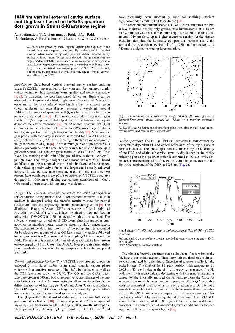
1040 nm vertical external cavity surfaceemitting laser based on InGaAs quantumdots grown in Stranski-Krastanow regime
A. Strittmatter, T.D. Germann, J. Pohl, U.W. Pohl,D. Bimberg, J. Rautiainen, M. Guina and O.G. Okhotnikov
Quantum dots grown by metal organic vapour phase epitaxy in theStranski-Krastanow regime are succesfully implemented for the firsttime as active media in optically pumped vertical external cavitysurface emitting lasers. To optimise the gain the quantum dots areengineered to match the excited state luminescence to the cavity reson-ance. Room temperature continuous-wave operation at 1040 nm wave-length is demonstrated. An output power of 280 mW is achieved,limited only by the onset of thermal rollover. The differential conver-sion efficiency is 6.7%.
Introduction: GaAs-based vertical external cavity surface emittinglasers (VECSELs) are regarded as key elements for numerous appli-cations owing to their excellent beam quality and power scalability[1, 2]. In particular, low-cost laser-based full-colour displays can beobtained by frequency-doubled, high-power GaAs-based VECSELsoperating in the near-infrared wavelength range. Maximum greencolour rendering for such displays requires a wavelength around1040 nm. A number of quantum well (QW) based devices have beenpreviously reported [3–5]. The narrow, temperature dependent gainspectra of QWs requires careful adjustment to the temperature depen-dence of the cavity resonance [6]. InGaAs-based quantum dot (QD)ensembles are an attractive alternative to QWs since they exhibit abroad gain spectrum and high temperature stability [7]. Matching thegain profile with the cavity resonance as needed for QW-VECSELs iseasily obtained with QD-VECSELs owing to the broad and comparablyflat gain spectrum of QDs [8].The maximum gain of a QD ensemble isdirectly proportional to the areal density which, for InGaAs-based QDsgrown in Stranski-Krastanow regime, is limited to 1010 to 1011 cm22 perlayer. The resulting modal gain of the ground state is about 4 to 6 cm21
per QD layer. The low gain might be one reason that a VECSEL basedon QDs has not been reported so far despite its theoretical advantages.Gain values approximately a factor of 3 larger can be easily achievedhowever if excited-state transitions are used. For the first time, wepresent here continuous-wave (CW) operation of VECSEL structuresdesigned for 1040 nm employing excited-state transitions of InGaAsQDs tuned to resonance with the target wavelength.
Design: The VECSEL structures consist of the active QD layers, asemiconductor Bragg mirror, and a confinement window. The gainmedium is designed using the transfer matrix method for normalsurface emission, and employing material parameters given in [9]. Thedistributed Bragg reflector (DBR) consisting of 35.5 pairs ofAl0.98Ga0.02As/Al0.2Ga0.8As l/4 layers yielded a nominal bottomreflectivity of 99.992% and 90 nm spectral width of the stopband. Thesub-cavity comprises a total of 13 QD layers placed in groups at anti-nodes of the standing optical wave separated by GaAs spacer layers.The exponentially decaying intensity of the pump light is accountedfor by placing two groups of three QD layers near the surface followedby two groups of two QD layers and three single QD layers towards theDBR. The structure is completed by an Al0.3Ga0.7As barrier layer grownon top capped by 10 nm GaAs. The AlGaAs layer prevents carrier diffu-sion towards the surface while being transparent to both the pump andlaser light.
Growth and characterisation: The VECSEL structures are grown onundoped 2-inch GaAs wafers using metal organic vapour phaseepitaxy with alternative precursors. The GaAs buffer layers as well asthe DBR layers are grown at 6858C. The QD and the GaAs spacerlayers are grown at 500 and 6008C, respectively. Growth rates of the bin-aries InAs, GaAs, and AlAs are extracted for all temperatures from X-raydiffraction spectra of In0.1Ga0.9As/GaAs and AlAs/GaAs superlattices.The DBR stopband and the cavity length are adjusted by optical reflec-tion spectra recorded by an optical spectrum analyser.
The QD growth in the Stranski-Krastanow growth regime follows theprocedure described in [10]. Initially deposited 2.7 monolayers ofIn0.65Ga0.35As transform to QDs during a 180s growth interruption.These parameters yield very high QD densities of 1 � 1011 cm22 and
ELECTRONICS LETTERS 14th February 2008 Vol.
have previously been successfully used for realising efficienthigh-power edge emitting QD laser diodes [11].
The ensemble photoluminescence (PL) of QD test structures exhibitsat low excitation density only ground state luminescence at 1115 nmwith 80 nm full width at half maximum (Fig. 1). Excited-state transitionsaround 1040 nm show up at higher excitation density. At the highestexcitation densities, the luminescence spectrum becomes nearly flatacross the wavelength range from 1150 to 980 nm. Luminescence at940 nm is assigned to wetting layer emission.
Fig. 1 Photoluminescence spectra of single InGaAs QD layer grown inStranski-Krastanow mode, excited at 532 nm with varying excitationdensities
E0, E1, WL, GaAs denote transitions from ground and first excited states, fromwetting layer, and from matrix, respectively
Device operation: The full QD VECSEL structure is characterised bytemperature-dependent PL and optical reflectance of the top surface atnormal incidence. The optical spectrum is composed by the reflectivityof the DBR and of the sub-cavity layers. A dip is seen in the highlyreflecting part of the spectrum which is attributed to the sub-cavity res-onance. The spectral position of the PL peak emission coincides with thedip in the stopband of the DBR at 1038 nm (Fig. 2).
Fig. 2 Reflectivity (R) and surface photoluminescence (PL) of QD VECSELstructure
Full and dashed curves refer to spectra recorded at room temperature and þ80 K,respectivelyInset: Schematic of sample structure
The whole reflectivity spectrum can be simulated if absorption of theQD layers is taken into account. Then, the width and depth of the dip canbe well simulated by assuming a Gaussian absorption profile for theexcited states. The shift of the PL peak position with temperature by0.075 nm/K is only due to the shift of the cavity resonance. The PLpeak intensity is monotonically decreasing with increasing temperaturescaused by the thermally induced carrier leakage from the QDs. Asexpected, the much broader emission spectrum of the QD ensembleleads to a constant overlap with the cavity resonance. Despite longgrowth time of about 4 h for the total cavity sequence there is no blueshift of the QD luminescence compared to calibration samples. Thishas been confirmed by measuring the edge emission from VECSELsamples. Such stability of the QDs against thermally driven diffusionprocesses is a consequence of improved growth conditions for the caplayers as well as for the spacer layers [12].
44 No. 4
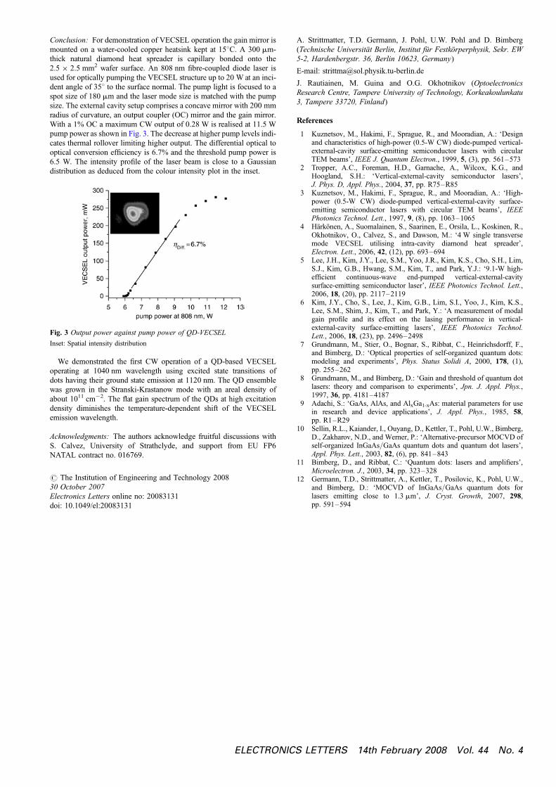
Conclusion: For demonstration of VECSEL operation the gain mirror ismounted on a water-cooled copper heatsink kept at 158C. A 300 mm-thick natural diamond heat spreader is capillary bonded onto the2.5 � 2.5 mm2 wafer surface. An 808 nm fibre-coupled diode laser isused for optically pumping the VECSEL structure up to 20 W at an inci-dent angle of 358 to the surface normal. The pump light is focused to aspot size of 180 mm and the laser mode size is matched with the pumpsize. The external cavity setup comprises a concave mirror with 200 mmradius of curvature, an output coupler (OC) mirror and the gain mirror.With a 1% OC a maximum CW output of 0.28 W is realised at 11.5 Wpump power as shown in Fig. 3. The decrease at higher pump levels indi-cates thermal rollover limiting higher output. The differential optical tooptical conversion efficiency is 6.7% and the threshold pump power is6.5 W. The intensity profile of the laser beam is close to a Gaussiandistribution as deduced from the colour intensity plot in the inset.
Fig. 3 Output power against pump power of QD-VECSEL
Inset: Spatial intensity distribution
We demonstrated the first CW operation of a QD-based VECSELoperating at 1040 nm wavelength using excited state transitions ofdots having their ground state emission at 1120 nm. The QD ensemblewas grown in the Stranski-Krastanow mode with an areal density ofabout 1011 cm22. The flat gain spectrum of the QDs at high excitationdensity diminishes the temperature-dependent shift of the VECSELemission wavelength.
Acknowledgments: The authors acknowledge fruitful discussions withS. Calvez, University of Strathclyde, and support from EU FP6NATAL contract no. 016769.
# The Institution of Engineering and Technology 200830 October 2007Electronics Letters online no: 20083131doi: 10.1049/el:20083131
ELECTRONIC
A. Strittmatter, T.D. Germann, J. Pohl, U.W. Pohl and D. Bimberg(Technische Universitat Berlin, Institut fur Festkorperphysik, Sekr. EW5-2, Hardenbergstr. 36, Berlin 10623, Germany)
E-mail: [email protected]
J. Rautiainen, M. Guina and O.G. Okhotnikov (OptoelectronicsResearch Centre, Tampere University of Technology, Korkeakoulunkatu3, Tampere 33720, Finland)
References
1 Kuznetsov, M., Hakimi, F., Sprague, R., and Mooradian, A.: ‘Designand characteristics of high-power (0.5-W CW) diode-pumped vertical-external-cavity surface-emitting semiconductor lasers with circularTEM beams’, IEEE J. Quantum Electron., 1999, 5, (3), pp. 561–573
2 Tropper, A.C., Foreman, H.D., Garnache, A., Wilcox, K.G., andHoogland, S.H.: ‘Vertical-external-cavity semiconductor lasers’,J. Phys. D, Appl. Phys., 2004, 37, pp. R75–R85
3 Kuznetsov, M., Hakimi, F., Sprague, R., and Mooradian, A.: ‘High-power (0.5-W CW) diode-pumped vertical-external-cavity surface-emitting semiconductor lasers with circular TEM beams’, IEEEPhotonics Technol. Lett., 1997, 9, (8), pp. 1063–1065
4 Harkonen, A., Suomalainen, S., Saarinen, E., Orsila, L., Koskinen, R.,Okhotnikov, O., Calvez, S., and Dawson, M.: ‘4 W single transversemode VECSEL utilising intra-cavity diamond heat spreader’,Electron. Lett., 2006, 42, (12), pp. 693–694
5 Lee, J.H., Kim, J.Y., Lee, S.M., Yoo, J.R., Kim, K.S., Cho, S.H., Lim,S.J., Kim, G.B., Hwang, S.M., Kim, T., and Park, Y.J.: ‘9.1-W high-efficient continuous-wave end-pumped vertical-external-cavitysurface-emitting semiconductor laser’, IEEE Photonics Technol. Lett.,2006, 18, (20), pp. 2117–2119
6 Kim, J.Y., Cho, S., Lee, J., Kim, G.B., Lim, S.I., Yoo, J., Kim, K.S.,Lee, S.M., Shim, J., Kim, T., and Park, Y.: ‘A measurement of modalgain profile and its effect on the lasing performance in vertical-external-cavity surface-emitting lasers’, IEEE Photonics Technol.Lett., 2006, 18, (23), pp. 2496–2498
7 Grundmann, M., Stier, O., Bognar, S., Ribbat, C., Heinrichsdorff, F.,and Bimberg, D.: ‘Optical properties of self-organized quantum dots:modeling and experiments’, Phys. Status Solidi A, 2000, 178, (1),pp. 255–262
8 Grundmann, M., and Bimberg, D.: ‘Gain and threshold of quantum dotlasers: theory and comparison to experiments’, Jpn. J. Appl. Phys.,1997, 36, pp. 4181–4187
9 Adachi, S.: ‘GaAs, AlAs, and AlxGa1-xAs: material parameters for usein research and device applications’, J. Appl. Phys., 1985, 58,pp. R1–R29
10 Sellin, R.L., Kaiander, I., Ouyang, D., Kettler, T., Pohl, U.W., Bimberg,D., Zakharov, N.D., and Werner, P.: ‘Alternative-precursor MOCVD ofself-organized InGaAs/GaAs quantum dots and quantum dot lasers’,Appl. Phys. Lett., 2003, 82, (6), pp. 841–843
11 Bimberg, D., and Ribbat, C.: ‘Quantum dots: lasers and amplifiers’,Microelectron. J., 2003, 34, pp. 323–328
12 Germann, T.D., Strittmatter, A., Kettler, T., Posilovic, K., Pohl, U.W.,and Bimberg, D.: ‘MOCVD of InGaAs/GaAs quantum dots forlasers emitting close to 1.3 mm’, J. Cryst. Growth, 2007, 298,pp. 591–594
S LETTERS 14th February 2008 Vol. 44 No. 4