Embed Size (px)
Citation preview

Annealing-induced change in quantum dot chain formation mechanismTyler D. Park, John S. Colton, Jeffrey K. Farrer, Haeyeon Yang, and Dong Jun Kim Citation: AIP Advances 4, 127142 (2014); doi: 10.1063/1.4905053 View online: http://dx.doi.org/10.1063/1.4905053 View Table of Contents: http://scitation.aip.org/content/aip/journal/adva/4/12?ver=pdfcov Published by the AIP Publishing Articles you may be interested in Presentation and experimental validation of a model for the effect of thermal annealing on thephotoluminescence of self-assembled InAs/GaAs quantum dots J. Appl. Phys. 107, 123107 (2010); 10.1063/1.3431388 Lateral ordering, strain, and morphology evolution of InGaAs/GaAs(001) quantum dots due to hightemperature postgrowth annealing Appl. Phys. Lett. 96, 083102 (2010); 10.1063/1.3299262 Annealing of self-assembled InAs/GaAs quantum dots: A stabilizing effect of beryllium doping Appl. Phys. Lett. 94, 072105 (2009); 10.1063/1.3086298 Raman spectroscopy of in situ annealed InAs/GaAs quantum dots J. Appl. Phys. 96, 1267 (2004); 10.1063/1.1762993 Formation of lateral quantum dot molecules around self-assembled nanoholes Appl. Phys. Lett. 82, 2892 (2003); 10.1063/1.1569992
All article content, except where otherwise noted, is licensed under a Creative Commons Attribution 3.0 Unported license. See:
http://creativecommons.org/licenses/by/3.0/ Downloaded to IP: 128.187.202.92 On: Thu, 01 Jan 2015 17:09:45
AIP ADVANCES 4, 127142 (2014)
Annealing-induced change in quantum dot chainformation mechanism
Tyler D. Park,1 John S. Colton,1,a Jeffrey K. Farrer,1 Haeyeon Yang,2and Dong Jun Kim31Department of Physics and Astronomy, Brigham Young University, Provo UT 84602, USA2Department of Nanoscience and Nanoengineering, South Dakota School of Minesand Technology, Rapid City, SD 57701, USA3IPG Photonics Corporation, Oxford, MA 01540, USA
(Received 26 September 2014; accepted 15 December 2014; published online 22 December2014)
Self-assembled InGaAs quantum dot chains were grown using a modified Stranski-Krastanov method in which the InGaAs layer is deposited under a low growthtemperature and high arsenic overpressure, which suppresses the formation of dotsuntil a later annealing process. The dots are capped with a 100 nm GaAs layer. Threesamples, having three different annealing temperatures of 460◦C, 480◦C, and 500◦C,were studied by transmission electron microscopy. Results indicate two distincttypes of dot formation processes: dots in the 460◦C and 480◦C samples form fromplatelet precursors in a one-to-one ratio whereas the dots in the sample annealed at500◦C form through the strain-driven self-assembly process, and then grow largervia an additional Ostwald ripening process whereby dots grow into larger dots at theexpense of smaller seed islands. There are consequently significant morphologicaldifferences between the two types of dots, which explain many of the previously-reported differences in optical properties. Moreover, we also report evidence ofindium segregation within the dots, with little or no indium intermixing betweenthe dots and the surrounding GaAs barrier. C 2014 Author(s). All article content,except where otherwise noted, is licensed under a Creative Commons Attribution 3.0Unported License. [http://dx.doi.org/10.1063/1.4905053]
In recent decades, quantum dots (QDs) have received large interest in the scientific commu-nity.1 Due to their discrete and tunable wavelength emission as well as their localized electronicstates, quantum dots have potential applications as lasers,2 detectors,3 optoelectronic devices,4 andquantum computing.5 Quantum dot size and morphology play a large role in the optical and elec-tronic properties,6 therefore investigations into growth techniques which allow for greater controlof the geometry and chemical composition are warranted. The most common technique for theself-assembly of epitaxial QDs is the Stranski-Krastanov (SK) method,7 where (for example) anInGaAs layer is grown on a GaAs substrate at temperatures of around 500◦C. The strain mismatchcauses the InGaAs layer to spontaneously form into dots once the layer reaches a critical thickness.
A new approach toward self-assembly has been used by several groups to achieve a greater con-trol of the resulting growth.8–11 In this modified SK technique, an InGaAs layer is grown at a coolertemperature than in the traditional technique, and under a high arsenic overpressure—both of whichsuppress the formation of dots by suppressing the detachment of atoms from the strained layerdue to the low thermal energy. This allows the InGaAs layer to grow thicker than the traditionalcritical thickness for spontaneous dot formation. Instead, the dots form at later annealing stageswhen the temperature is sufficiently increased. These modifications introduce new control variablesinto the growth process, such as InGaAs layer thickness and annealing temperature. By adjustingthese and other growth parameters, Kim et al. were able to affect the shape and morphology of
aE-mail: [email protected]
2158-3226/2014/4(12)/127142/9 4, 127142-1 ©Author(s) 2014
All article content, except where otherwise noted, is licensed under a Creative Commons Attribution 3.0 Unported license. See:
http://creativecommons.org/licenses/by/3.0/ Downloaded to IP: 128.187.202.92 On: Thu, 01 Jan 2015 17:09:45
127142-2 Park et al. AIP Advances 4, 127142 (2014)
the dots; for example, the dots could be formed into self-assembled chains.9 In addition to allow-ing for interesting morphologies, the low temperature growth is believed to suppress deleteriouseffects of indium segregation (indium clumping at the top of dots), evaporation, and intermixing(indium seeping into the substrate from the wetting layer),12,13 which cause inhomogeneity inthe indium concentration. Chaining of dots has also been obtained using other techniques suchas e-beam lithography14 and cleaved edge overgrowth,15 superlattice growth,16,17 and exploitingstrain fluctuations in dislocation-patterned templates18—but these typically involve an underlyingpattern whereas the low temperature modified SK growth technique allows chain formation throughself-assembly of dots into chains from a single InGaAs layer.
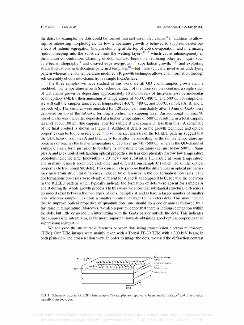
The three samples we have studied in this work are all QD chain samples grown via themodified, low temperature growth SK technique. Each of the three samples contains a single stackof QD chains grown by depositing approximately 10 monolayers of In0.40Ga0.60As by molecularbeam epitaxy (MBE), then annealing at temperatures of 460◦C, 480◦C, and 500◦C. For simplicity,we will call the samples annealed at temperatures 460◦C, 480◦C, and 500◦C, samples A, B, and Crespectively. The samples were annealed for 120 seconds; immediately after, 10 nm of GaAs weredeposited on top of the InGaAs, forming a preliminary capping layer. An additional nominal 90nm of GaAs was thereafter deposited at a higher temperature of 580◦C, resulting in a total cappinglayer of about 100 nm (the capping layer for sample B was somewhat less than this). A schematicof the final product is shown in Figure 1. Additional details on the growth technique and opticalproperties can be found in reference;19 to summarize, analysis of the RHEED patterns suggest thatthe QD-chains of samples A and B actually form after the annealing, as the sample temperature ap-proaches or reaches the higher temperature of cap layer growth (580◦C), whereas the QD-chains ofsample C likely form just prior to reaching its annealing temperature (i.e. just below 500◦C). Sam-ples A and B exhibited outstanding optical properties such as exceptionally narrow low temperaturephotoluminescence (PL) linewidths (<20 meV) and substantial PL visible at room temperature,and in many respects resembled each other and differed from sample C (which had similar opticalproperties to traditional SK dots). This caused us to propose that the differences in optical propertiesmay arise from structural differences induced by differences in the dot formation processes. (Thedot formations processes were clearly different for A and B as compared to C, because the chevronsin the RHEED pattern which typically indicate the formation of dots were absent for samples Aand B during the whole growth process.) In this work we show that substantial structural differencesdo indeed exist between the two types of dots. Samples A and B have a larger number of smallerdots, whereas sample C exhibits a smaller number of larger (but shorter) dots. This may indicatethat to improve optical properties of quantum dots, one should do a cooler anneal followed by afast raise in temperature. Moreover, we also report evidence that there is indium segregation withinthe dots, but little or no indium intermixing with the GaAs barrier outside the dots. This indicatesthat suppressing intermixing is far more important towards obtaining good optical properties thansuppressing segregation.
We analyzed the structural differences between dots using transmission electron microscopy(TEM). Our TEM images were mainly taken with a Tecnai TF-30 TEM with a 300 keV beam, inboth plan-view and cross-section view. In order to image the dots, we used the diffraction contrast
FIG. 1. Schematic diagram of a QD chain sample. The samples are reported to be pyramidal in shape9 and often overlappartially from dot to dot.
All article content, except where otherwise noted, is licensed under a Creative Commons Attribution 3.0 Unported license. See:
http://creativecommons.org/licenses/by/3.0/ Downloaded to IP: 128.187.202.92 On: Thu, 01 Jan 2015 17:09:45

127142-3 Park et al. AIP Advances 4, 127142 (2014)
method with a (220) two-beam condition. This creates visible strain contrast due to lattice distor-tions on the (220) planes which are caused by the self-assembled QDs. Techniques for imaging thedots in our samples are similar to those explained in Reference 20.
In order for the 300 keV beam to pass through GaAs samples, the samples must be less than100 nm thick; we therefore had to develop methods for preparing different “cuts” (very smallpieces) of the samples which included the dot-containing regions. To obtain cross-section cuts, weperformed a lift-out via a FEI Helios Nanolab 600 FIB/SEM scanning electron microscope (SEM)with a Ga+ focused ion beam (FIB) mill.21 This is done by milling out a pit on either side of a1 µm × 10 µm rectangle, to a depth of ∼5 µm (see Figure 2a). The 1 × 10 × 5 µm cut is then attachedto an OmniProbe needle, separated from the substrate, lifted out from the pit, and mounted on acopper TEM grid where it is thinned further with the FIB to final dimensions of ∼0.1 × 10 × 5 µm.Chemical analysis was performed on the cross-section cuts on a Tecnai TF20 analytical transmis-sion electron microscope equipped for energy dispersive X-ray spectroscopy (XEDS or EDS). Thebeam size for the EDS analysis was typically smaller than 1 nm × 1 nm. Line scans were performedvia a sequence of points taken across the InGaAs region (wetting layer and dots), having dwelltimes of 10-20 s. Images from the cross-section cuts were used to characterize both the height of thestrain field produced by the dots and the distribution of indium across the dot layer.
Plan-view cuts were obtained using a slightly different method. For sample C, the cut wasprepared in a lift-out method similar to the cross-section cuts; see Figure 2b. In this case, a pit ismilled out from the edge just below the intended cut, then the cut is bonded to the OmniProbeneedle and lifted out. However, this proved challenging to reproduce. Therefore for samples A andB, we used a hybrid method of hand polishing and FIB thinning.22 In this method, we attach part ofthe sample to a tripod polisher and thin the sample down close to 1 µm, at approximately a 1◦ angle;see Figure 3. The sample is then mounted to a copper half-washer and an area is thinned to therequired 100 nm with the FIB, resulting in a usable portion with final dimensions of approximately0.1 × 20 × 5 µm. TEM images from the plan-view cuts were used to characterize dot sizes, dotspacings within chains, the spacings between chains, and overall dot density.
Figure 4 shows representative plan-view images of each of our samples. It is evident thatdot-chains exist in all three samples, similar to those reported for uncapped8,9 and partially-cappedQD chains.10 We analyzed these and other similar plan-view TEM images to obtain average valuesand standard deviations within the populations for the various parameters describing the dots’morphology. Dot widths were obtained as full-width half-max (FWHM) values via the softwareprogram ImageJ. Specifically, intensity line profiles were first plotted, which due to the apparentshadowing caused by the TEM (i.e. different facets interacting with the (220) beam conditiondifferently) had a sigmoidal profile. The sigmoidal curves were then differentiated to obtain aGaussian-like dot profile, from which the FWHM was extracted and recorded as the dot size. Thiswas done with 30 measurements per sample in a random selection of visible dots over three or four
FIG. 2. Lift-out cuts in preparation in the FIB/SEM. (a) A cross-section cut is prepared by milling out pits on both sides ofthe desired area. This image is a top-down view in the [001] direction. (b) A plan-view cut is prepared by milling out the areaunderneath the desired cut. This image is looking at a [110] surface of our sample. Since the dots are approximately 100 nmfrom the top surface the cut was prepared as a wedge, tapering in as it goes away from the [110] surface. The thinnest portionof the cut was then studied in the TEM.
All article content, except where otherwise noted, is licensed under a Creative Commons Attribution 3.0 Unported license. See:
http://creativecommons.org/licenses/by/3.0/ Downloaded to IP: 128.187.202.92 On: Thu, 01 Jan 2015 17:09:45

127142-4 Park et al. AIP Advances 4, 127142 (2014)
FIG. 3. Diagram of a sample prepared using the hybrid method. Mechanical thinning was done from the underside of thesample (i.e. the top of this diagram) at a small angle from the surface. Once the mechanical thinning limits were reached(1 − 5 µm), the FIB/SEM was used for the final milling and cutting (see inset).
images per sample. The average values and standard deviations are given in Table I. Dot separationswithin a chain and the number of chains per unit length were similarly measured, and total dot den-sity (dots/cm2) was calculated by multiplying the inverse of the former by the latter. These valuesare also given in Table I. To summarize, samples A and B had very similar dot widths (10-11 nm),dot separations (11 nm), chain densities (3 × 105 cm−1), and dot densities (2 − 3 × 1011 cm−2).Conversely, the dots in sample C were substantially larger (25 nm) and more separated (34 nm), hada lower density of chains (2 × 105 cm−1), and a lower overall density of dots (0.6 × 1011 cm−2). As isevident, there is a significant difference in morphology between the two types of dots.
Comparing these samples with others in the literature, we find that the dot density in sam-ples A and B is extremely high. It is smaller than GaAs dots prepared by low temperature dropletepitaxy (7.3 × 1011 cm−2) but larger than any others reported using strain-driven self-assembly(1.4 × 1011 cm−2 maximum).23,24 In addition, images from our samples don’t show the large clumpsof dots which have been a problem in other low-temperature SK-grown samples when the densitybecomes larger than 7.5 × 1010 cm−2.24 The authors of Reference 24 indicated that the presence ofclumps was the main reason why their high density dots are not suitable for solar cell applications,namely that the high strain induced by the large clumps penetrates into the upper layers duringstacking, generating nonradiative recombination centers and decreasing the radiative conversionefficiency. In contrast, our dots show high optical quality, demonstrated by narrow PL linewidthsand light emission from these dots at room temperature.19
The observed dot size for samples A and B is comparable to the size of the GaAs dots mentionedabove grown via low temperature droplet epitaxy.23 Those dots were grown on GaAs(311) substratesat temperatures below 100◦C, and were extremely closely packed; a dot density of 7.3 × 1011 cm−2
yields an average dot separation distance of 11.7 nm. Our dots are as closely packed along thechain direction, 11 ± 2 nm, but overall less closely packed due to the separation between chains.The difference is undoubtedly due to the strain-driven nature of our process, the formation being
FIG. 4. TEM images of QD chains seen in plan-view cuts from the samples annealed at (a) 460◦C, (b) 480◦C, and (c) 500◦C.Note the difference in scale between (c) compared to (a) and (b).
All article content, except where otherwise noted, is licensed under a Creative Commons Attribution 3.0 Unported license. See:
http://creativecommons.org/licenses/by/3.0/ Downloaded to IP: 128.187.202.92 On: Thu, 01 Jan 2015 17:09:45

127142-5 Park et al. AIP Advances 4, 127142 (2014)
TABLE I. Physical measurements taken from the plan-view TEM images.
SampleDot widths
(FWHM, nm)Dot separation
(nm)Dot-chain density
(× 105 cm−1)Dot density
(× 1011 cm−2)
A (460◦C) 10.7 ± 2.3 11.0 ± 1.9 2.7 ± 1.4 2.4 ± 1.3B (480◦C) 10.2 ± 1.7 11.1 ± 2.7 3.0 ± 0.8 2.7 ± 1.0C (500◦C) 24.8 ± 4.9 34.4 ± 12.9 1.9 ± 0.2 0.6 ± 0.2
mediated by the mean strain field25 coupled with elastic relaxation that prefers elongated structuressuch as quantum wires,26 as opposed to the non strain-based droplet epitaxy used by that group.
Figure 5 presents a scanning tunneling microscope (STM) image, as-deposited, of a samplesimilar to samples A, B, and C, taken prior to annealing and dot formation. One monolayer thickplatelets are visible. A comparison of this and other STM images from the InGaAs epilayers withthe TEM images of the capped QD-chains indicate that the platelet density is the same as the dotdensity of samples A and B. This suggests that the platelets are precursors of the dots, somethingwhich also has been proposed by numerous theoretical works.25,27–29 The platelets develop into dotsduring the subsequent capping processes at higher temperatures in samples A and B, while theygrow into dots during the ramping up and annealing period in sample C. The apparent discrepancybetween the STM images of platelet precursors being randomly distributed and the finished dotsappearing in chains may be explained by the dot formation, once allowed to take place, being driveninto elongated shapes to better provide elastic relaxation of stress similar to what has been seen inquantum wires.26
Figure 6 shows representative cross-section images for our three samples. The light and darkregions indicate the presence of localized strain fields, which again confirm the existence of indi-vidual quantum dots in all three samples. The contrasting regions occur as the lattice bends intodifferent Bragg conditions; i.e. the dark region is farther from the (220) condition than the white
FIG. 5. High resolution, in-vacuum STM image from an as-grown InGaAs surface. The InGaAs epilayer thickness is10.24 ML, grown on GaAs(001) at low temperature (360◦C). The arrow is along the [110] direction. The circles denotethe positions of platelets that are 1 monolayer thick.
All article content, except where otherwise noted, is licensed under a Creative Commons Attribution 3.0 Unported license. See:
http://creativecommons.org/licenses/by/3.0/ Downloaded to IP: 128.187.202.92 On: Thu, 01 Jan 2015 17:09:45

127142-6 Park et al. AIP Advances 4, 127142 (2014)
FIG. 6. TEM images of strains of QDs seen in cross-section cuts from the samples annealed at (a) 460◦C, (b) 480◦C, and(c) 500◦C. This image is looking at a [11̄0] surface of our sample, where the chains and the indium-containing plane extend“into the page”. The vertical direction perpendicular to the indium-containing plane is [001]. The white arrows indicate theextent of the strain fields, providing an upper bound on the height of the dots.
region. The white arrows in the images indicate our estimates for the strain fields for some repre-sentative cases. Since the strain fields extend beyond the QDs themselves, our measurements of theextent of the strain provide only an upper bound on the height of the dots. Measurements of thestrain field heights across many images are 21.7 ± 4.1 nm, 30.8 ± 5.0 nm and 13.8 ± 3.6 nm forsamples A, B, and C respectively. These numbers can only roughly be compared, however, sinceimaging and sample conditions such as sample thickness, sample warping, or being “off-zone” maycontribute to how much of the strain fields are visible—so, for example, we cannot conclude that thedots in sample B are taller than the dots in sample A (they may well be shorter, as is discussed ina later paragraph). Roughly speaking, however, this seems to indicate that sample C contains flatterdots than samples A and B.
The cross-section cuts were also used for the EDS measurements on chemical composition todetermine the distribution of indium in the samples. As mentioned above, line measurements weredone as a series of point measurements across the indium-containing region (wetting layer anddots). Since the EDS beam probes all the way through the cross-section, a large percentage of thevolume being probed will be GaAs in addition to InGaAs; therefore, the EDS measurements can beused to verify the presence and measure the distribution of indium, but not to establish the specificindium composition percentage. The EDS results are presented in Figure 7. The curves in the figurehave been normalized, shifted vertically for clarity, and fitted to Gaussian curves. A summary ofthe strain field measurements and the indium distribution widths is found in Table II. (The reportedindium distribution widths are the 1/e2 widths from the Gaussian fits.)
If the indium were distributed uniformly throughout the dots, one would expect the base of thedots (left hand side of the displayed peaks in Fig. 7) to have a higher amount of indium than thepeak of the dots (right hand side), and the peaks in Fig. 7 would be asymmetric. This is becauseas the TEM passes through the base of the dots, a greater fraction of the material being probed isInGaAs dots and a smaller fraction is GaAs barrier. In our measured data of Fig. 7 there may be aslight asymmetry present, skewed in that direction, but if so it is small—as is evidenced by the abil-ity of the Gaussian curves to adequately fit the data. The presence of symmetry in the Fig. 7 peakstherefore seems to indicate that the indium is segregating vertically, i.e. rising towards the tops ofthe dots. This is consistent with the concept of “floating indium”,30 and uneven distribution of in-dium in QDs due to segregation has been reported in other samples—for example, in measurementsfrom energy selective imaging in uncapped InGaAs QDs12 and cross-sectional scanning tunneling
All article content, except where otherwise noted, is licensed under a Creative Commons Attribution 3.0 Unported license. See:
http://creativecommons.org/licenses/by/3.0/ Downloaded to IP: 128.187.202.92 On: Thu, 01 Jan 2015 17:09:45

127142-7 Park et al. AIP Advances 4, 127142 (2014)
FIG. 7. EDS line scans through the InGaAs sections (wetting layer and dots) of samples A, B, and C (460◦C, 480◦C, and500◦C), showing amount of indium present. The solid lines are Gaussian fits to the data.
microscopy (STM) of capped InGaAs QDs.31 However, the low temperature growth should sup-press the segregation process. Our findings therefore indicate that the higher temperatures in thelater stages (annealing and subsequent capping) are sufficient to allow for indium atoms to rise tothe top of the dots.
The measured 1/e2 widths of the indium distributions in our samples are 7.1 nm, 5.3 nm,and 3.5 nm, for samples A, B, and C, respectively. All three of these numbers are less than themeasured heights of QDs in a similar, uncapped sample annealed at 460◦C, measured through STM(8.3 nm, Ref. 8). Therefore it seems likely little or no intermixing of indium with the surroundingGaAs is occurring despite the higher annealing temperatures (for samples B and C; sample A isthe same) and even higher temperatures during final capping (for all three samples). Those widthstherefore provide a lower bound estimate of the height of the dots, the strictness of the boundbeing determined by the degree of segregation. These results support the indication from the strainfield measurements mentioned above that sample C’s dots are flatter than the others, and may wellindicate that sample B’s dots are flatter than sample A’s. This is consistent with our PL peak positiondata which found that sample C had the highest PL peak energy, followed by sample B and thensample A.19 Since all three samples have the same nominal indium concentration, the dominantfactor in establishing differences in peak position will be quantum confinement, particularly in thesmallest dimension. Sample C therefore has the largest quantum confinement shift in PL energy dueto the very short height of its dots (despite its overall greater average volume per dot). This assign-ment of dot heights being shortest for C, then B, then A, also matches the findings of Kim et al.,who reported a flattening of dots in other dot-chain samples with increasing annealing temperature.8
When the cross-section data is combined with the plan-view data, they then indicate sample Chas larger dot width, smaller dot height, larger separation between dots, larger chain separations,and a much smaller overall dot density compared to samples A and B. These differences can all
TABLE II. Physical measurements taken from the cross-section TEM images.
Sample Strain field height (nm) Indium region height (nm)
A (460◦C) 21.7 ± 4.1 7.1 ± 0.6B (480◦C) 30.8 ± 5.0 5.3 ± 0.4C (500◦C) 13.8 ± 3.6 3.5 ± 0.2
All article content, except where otherwise noted, is licensed under a Creative Commons Attribution 3.0 Unported license. See:
http://creativecommons.org/licenses/by/3.0/ Downloaded to IP: 128.187.202.92 On: Thu, 01 Jan 2015 17:09:45

127142-8 Park et al. AIP Advances 4, 127142 (2014)
be explained by Ostwald ripening occurring in sample C during the 120 second annealing period.Ostwald ripening, i.e. the growth of larger particles at the expense of smaller seed particles, hasbeen shown to occur in Si/Ge systems (Ge islands on Si substrate) in time scales of 20 seconds.32
In an InGaAs system, namely InGaAs islands on a GaAs substrate and an annealing temperature of450◦C, substantial ripening occurred in 5 minutes.33 Our sample C was annealed at a temperature of500◦C, thus one would expect shorter ripening times than their time of 5 minutes. Our observationsof larger dots in sample C therefore make sense with substantial ripening having occurred during the120 second annealing period. Samples A and B, conversely, exhibited no ripening. This verifies theRHEED data from Ref. 19 (mentioned above) which suggested that the dots in samples A and B hadnot yet formed during the 120 s period of annealing. If the dots form later in the growth, then there isnot enough time at high temperatures for ripening to occur.
As we have mentioned above, samples A and B exhibited much better optical properties thansample C, and (similarly) much better than the typical SK grown dots. Moreover, the optical dataled us to propose that samples A and B may have a much more uniform size distribution than sam-ple C.19 These TEM data don’t support that hypothesis for the lateral dimensions; the uniformityof the size distribution, as measured by the ratio of the population standard deviation to averagedot width, is fairly comparable for all three dots. However, for the out-of-plane dimension (i.e. theheights), sample C did have a noticeably larger non-uniformity in its strain profiles than samplesA and B, as measured by a similar ratio. Its standard deviation/height ratio is 26%, compared to19% and 16% for samples A and B, respectively. Although the out-of-plane measurements are notas precise as the lateral measurements (as discussed above), this is at least consistent with the dotsin samples A and B being more uniform in their optical properties. Since quantum confinementeffects depend very strongly and nonlinearly on structural dimensions, and since this is the smallestdimension of the QDs, any non-uniformity in this dimension will have magnified effects in theelectronic and hence optical uniformity. The data therefore indicate that in order to produce dotswith the best possible optical properties, one should emphasize growth techniques which cause lessflattening of the dots.
In conclusion, we have used TEM techniques to make quantitative structural and composi-tional measurements in self-assembled InGaAs QD chains. The TEM results demonstrate that themorphology of the dots annealed at 460◦C and 480◦C is quite similar, but the morphology changesabruptly as the annealing temperature is raised from 480◦C to 500◦C. In other words, there is acritical annealing temperature above which the dots flatten out, the widths increase, the heightsdecrease, and both the dot density within the chains and the dot-chain density decrease. This isconsistent with, and explained by, previous results which indicated that the SK transition to dotsoccurs at a later point in the growth process for the 460◦C and 480◦C annealed samples comparedto the 500◦C sample. The 500◦C sample features substantial Ostwald ripening due to its earlierdot formation and relatively high annealing temperature. EDS measurements on indium concentra-tion support the claim that this modified SK method creates dots with little intermixing into thesurrounding GaAs, but may indicate indium segregation towards the peak of the pyramidal dots isstill occurring. The 460◦C and 480◦C samples additionally have very good optical properties, asreported earlier; thus this structural data indicates that small dots, closely spaced into chains, butwithout the clumping that can occur in other strain-driven methods, can be a good system for futureoptical device applications.
ACKNOWLEDGMENTThe work is supported by the National Aeronautics and Space Administration (Cooperative
Agreement Number: NNX13AD31A). Also financial support from the National Science Founda-tion, grant numbers 0854313, 0903804 and 114 3543 is gratefully acknowledged.1 M. A. Reed, J. N. Randal, R. J. Aggarwal, R. J. Matyi, T. M. Moore, and A. E. Wetsel, “Obseration of discrete electronic
states in a zero-dimensional semiconductor nanostructure,” Physical Review Letters 60, 535 (1988).2 V. A. Egorov, G. E. Cirlin, N. K. Polyakov, V. N. Petrov, A. A. Tonkikh, B. V. Volovik, Y. G. Musikhin, A. E. Zhukov, A.
F. Tsatsulnikov, and V. M. Ustinov, “1.3 − 1.4 µm photoluminescence emission from InAs/GaAs quantum dot multilayerstructures grown on GaAs singular and vicinal substrates,” Nanotechnology 11, 323–326 (2000).
All article content, except where otherwise noted, is licensed under a Creative Commons Attribution 3.0 Unported license. See:
http://creativecommons.org/licenses/by/3.0/ Downloaded to IP: 128.187.202.92 On: Thu, 01 Jan 2015 17:09:45

127142-9 Park et al. AIP Advances 4, 127142 (2014)
3 H. C. Liu, M. Gao, J. McCaffrey, Z. R. Wasilewski, and S. Fafard, “Quantum dot infrared photodetectors,” Applied PhysicsLetters 78, 79–81 (2001).
4 P. Bhattacharya, S. Ghosh, and A. Stiff-Roberts, “Quantum dot opto-electronic devices,” Annu. Rev. Mater. Res. 34, 1–40(2004).
5 S. Bose, “Quantum communication through an unmodulated spin chain,” Physical Review Letters 91, 1–4 (2003).6 Y. Li, O. Voskoboynikov, C. P. Lee, S. M. Sze, and O. Tretyak, “Electron energy state dependence on the shape and size of
semiconductor quantum dots,” Journal of Applied Physics 90, 12 (2001).7 I. N. Stranski and L. von Krastanow, Abhandlungen der Mathematisch-Naturwissenschentlichen Klasse IIb 146, 797–810
(1938).8 D. J. Kim, E. A. Everett, and H. Yang, “Annealing induced transition of flat strained InGaAs epilayers into three-dimensional
islands,” Journal of Applied Physics 101, 106106 (2007).9 D. J. Kim and H. Yang, “Shape control of InGaAs nanostructures on nominal GaAs(001): dashes and dots,” Nanotechnology
19, 475601 (2008).10 K. N. Chauhan, D. M. Riffe, E. A. Everett, D. J. Kim, H. Yang, and F. K. Shen, “Carrier capture dynamics of single In-
GaAs/GaAs quantum-dot layers,” Journal of Applied Physics 113, 203710 (2013).11 O. G. Schmidt, O. Kienzle, Y. Hao, K. Eberl, and F. Ernst, “Modified Stranski-Krastanov growth in stacked layers of
self-assembled islands,” Applied Physics Letters 74, 1272–1274 (1999).12 T. Walther, A. G. Cullis, D. J. Norris, and M. Hopkinson, “Nature of the Stranski-Krastanow transition during epitaxy of
InGaAs on GaAs,” Physical Review Letters 86, 2381–2384 (2001).13 G. Biasiol, S. Heun, G. B. Golinelli, A. Locatelli, T. O. Mentes, F. Z. Guo, C. Hofer, C. Teichert, and L. Sorba, “Surface
compositional gradients of InAs/GaAs quantum dots,” Applied Physical Letters 87, 223106 (2005).14 T. V. Hakkarainen, J. Tommila, A. Schramm, A. Tukiainen, R. Ahorinta, M. Dumitrescu, and M. Guina, “Structural charac-
terization of InAs quantum dot chains grown by molecular beam epitaxy on nanoimprint lithography patterned GaAs(100),”Nanotechnology 22, 295604 (2001).
15 E. Uccelli, M. Bichler, S. Nürnberger, G. Abstreiter, and A. F. i Morral, “Controlled synthesis of InAs wires, dot, and twin-dotarray configurations by cleaved edge overgrowth,” Nanotechnology 19, 045303 (2008).
16 P. M. Petroff and S. P. DenBaars, “MBE and MOCVD growth and properties of self-assmebling quantum dot arrays in III-Vsemiconductor structures,” Superlattices and Microstructures 15, 1 (1994).
17 Z. M. Wang, K. Holmes, Y. I. Mazur, and G. Salamo, Applied Physics Letters 84, 1931 (2004).18 T. V. Hakkarainen, A. Schramm, A. Tukiainen, R. Ahorinta, L. Toikkanen, and M. Guina, “Lateral ordering of InAs quantum
dots on cross-hatch patterned GaInP,” Nanoscale Res. Lett. 5, 1892 (2010).19 H. Yang, D. J. Kim, J. Colton, T. Park, D. Meyer, A. M. Jones, S. Thalman, D. Smith, K. Clark, and S. Brown, Growth and
temperature dependent photoluminescence of InGaAs quantum dot chains. Applied Surface Science, available online 14Jan 2014, ISSN 0169-4332, http://dx.doi.org/10.1016/j.apsusc.2013.12.176.
20 J. P. McCaffrey, M. D. Robertson, S. Fafard, Z. R. Wasilewski, E. M. Griswold, and L. D. Madsen, “Determination of thesize, shape, and composition of indium-flushed self-assembled quantum dots by transmission electron microscopy,” Journalof Applied Physics 88, 2272 (2000).
21 F. A. Stevie, C. B. Vartuli, L. A. Giannuzi, T. L. Shofner, S. R. Brown, B. Rossie, F. Hillion, R. H. Mills, M. Antonell, R.B. Irwin, and B. M. Purcell, “Application of focused ion beam lift-out specimon preparation to TEM, SEM, STEM, AES,and SIMS analysis,” Surface and Interface Analysis 31, 345–351 (2001).
22 R. Anderson and S. J. Klepeis, “Combined tripod polishing and FIB method for preparing semiconductor plan view speci-mens,” MRS Proceedings 480, 187 (1997).
23 M. Jo, T. Mano, Y. Sakuma, and K. Sakoda, “Extremely high-density GaAs quantum dots grown by droplet epitaxy,” AppliedPhysics Letters 100, 212113 (2012).
24 D. Zhou, G. Sharma, S. F. Thomassen, T. W. Reenaas, and B. O. Fimland, “Optimization towards high density quantumdots for intermediate band solar cells grown by molecular beam epitaxy,” Applied Physics Letters 96, 061913 (2010).
25 Y. Chen and J. Washburn, “Structural transition in large-lattice-mismatch heteroepitaxy,” Physical Review Letters 77, 4046(1996).
26 J. Tersoff and R. M. Tromp, “Shape transition in growth of strained islands: spontaneous formation of quantum wires,”Physical Review Letters 70, 2782 (1993).
27 C. Priester and M. Lannoo, “Origin of self-assembled quantum dots in highly mismatched heteroepitaxy,” Physical ReviewLetters 75, 93 (1995).
28 H. T. Dobbs, D. D. Vvedensky, A. Zangwill, J. Johansson, N. Carlsson, and W. Seifert, “Mean-field theory of quantum dotformation,” Physical Review Letters 79, 897 (1997).
29 A. Li, F. Liu, D. Y. Petrovykh, J.-L. Lin, J. Viernow, F. J. Himpsel, and M. G. Lagally, “Creation of quantum platelets viastrain-controlled self-organization at steps,” Physical Review Letters 85, 5380 (2000).
30 P. Howe, E. C. Le Ru, E. Clarke, R. Murray, and T. S. Jones, “Quantification of segregation and strain effects in In As GaAs quantum dot growth,” Journal of Applied Physics 98, 113511 (2005).
31 N. Liu, J. Tersoff, O. Baklenov, A. L. Holmes, Jr., and C. K. Shih, “Nonuniform composition profile in In0.5Ga0.5As alloyquantum dots,” Physical Review Letters 84, 334–337 (2000).
32 F. M. Ross, J. Tersoff, M. Reuter, F. K. Legoues, and R. M. Tromp, “In situ transmission electron microscopy observationsof the formation of self-assembled Ge islands on Si,” Microscopy Research and Technique 42, 281–294 (1998).
33 L. Ke, Z. Qing, Z. Xun, G. Xiang, L. Zi-Jiang, W. Ji-Hong, H. Ming-Zhe, and D. Zhao, “Ripening of single-layer InGaAsislands on GaAs (001),” Chin. Phys. B 22, 026801 (2013).
All article content, except where otherwise noted, is licensed under a Creative Commons Attribution 3.0 Unported license. See:
http://creativecommons.org/licenses/by/3.0/ Downloaded to IP: 128.187.202.92 On: Thu, 01 Jan 2015 17:09:45