Embed Size (px)
Citation preview

InGaAs surface preparation for atomic layer deposition by hydrogen cleaningand improvement with high temperature anneal
Wilhelm Melitz,1,2 Jian Shen,1,2 Tyler Kent,1,2 Andrew C. Kummel,2,a) and Ravi Droopad3
1Materials Science and Engineering Program, University of California, San Diego, La Jolla, California92093, USA2Department of Chemistry and Biochemistry, University of California, San Diego, La Jolla, California 92093,USA3Department of Physics, Texas State University, San Marcos, Texas 78666, USA
(Received 18 January 2011; accepted 8 May 2011; published online 11 July 2011)
Using in situ atomic scale imaging with scanning tunneling microscopy/spectroscopy, a
combination of atomic hydrogen dosing, annealing, and trimethyl aluminum dosing is observed to
produce an ordered unpinned passivation layer on an air exposed InGaAs(001)-(4� 2) surface with
only monatomic steps. This shows that conventional gate-last semiconductor processing can
be employed to fabricate a variety of electronic devices, even on air exposed compound
semiconductors. VC 2011 American Institute of Physics. [doi:10.1063/1.3597791]
INTRODUCTION
Commercial III-V semiconductor devices such as high
electron mobility transistors and heterostructure bipolar tran-
sistor all employ interfaces, which are grown in situ in vac-
uum systems to avoid air contamination of the III-V
surfaces. However, these devices are not suitable for practi-
cal logic applications such as microprocessors because they
cannot be scaled in size and have large off-state leakage cur-
rents. At present, the only device design which offers the
compact size and low off-state currents required for micro-
processors is the metal oxide semiconductor field effect tran-
sistor (MOSFET). Present MOSFETs are fabricated on
silicon, but higher levels of integration (more devices per
unit area) are limited by power dissipation; therefore, several
hundred research papers are published each year upon the
development of MOSFETs using III-V semiconductors,
especially InGaAs.1 To enable low power MOSFET opera-
tion, a low supply voltage is required, the semiconductor
must have high mobility and high saturation velocity, the ox-
ide-semiconductor interface must have a low density of
interface trap states (Dit), and the oxide-semiconductor inter-
face must be nearly atomically flat to insure high mobility at
high field strength.
Surface channel III-V MOS devices can be fabricated
with atomic layer deposition (ALD) high-K gate-first proc-
esses,2–5 which are similar to silicon processes for SiO2
growth on silicon or ALD of high-K on silicon.6–10 The key
for a gate-first process is that subsequent processing steps
cannot degrade the semiconductor, the dielectric, or the ox-
ide-semiconductor interfaces. For silicon, the only commer-
cial ALD high-K fabrication process is a replacement gate
process (a type of gate-last process) to avoid processing-
induced damage.11 While preparing silicon for gate-last
processing is straightforward, for III-V semiconductors the
key to a gate-last process is the order and cleanliness of the
III-V channel prior to dielectric deposition. It has been
shown that ALD of trimethyl aluminum (TMA)12,13 or tetra-
kis(ethylmethylamino)hafnium (TEMAH)14 on III-V semi-
conductors has self-cleaning properties by reducing the
presence of As–O and Ga–O bonds. However, for high qual-
ity dielectric semiconductor interfaces, further reduction or
cleaning may be required and the interface must be atomi-
cally flat. Furthermore, aggressive oxide thickness reduction
[equivalent oxide thickness (EOT) scaling] is needed to fab-
ricate small gate length devices with small subthreshold
swings, and aggressive EOT scaling requires a very high uni-
form ALD nucleation density with no pinholes due to surface
contaminants.15 The key barrier to solving a very practical
problem is a surface chemistry challenge: development of a
chemical process, which removes nearly all air induced
defects and contaminants and leaves the III-V surface flat
and electrically active for high nucleation density ALD gate
oxide deposition which unpins the Fermi level.
Atomic hydrogen cleaning of III-V semiconductors has
been investigated.16–22 Traditional atomic hydrogen cleaning
is performed at elevated temperatures as a surface prepara-
tion for molecular beam epitaxial (MBE) growth. This study
investigates the hydrogen cleaning at 24 and 380 �C with
postcleaning annealing to determine the influences of clean-
ing temperature and annealing temperature on the electronic
structure and surface defects, roughness, and step density.
Atomic hydrogen has been shown to unpin GaAs,22 however,
it induces surface etching.21,23,24 It has been shown that the
atomic hydrogen etch rate for silicon is lower at 700 �C com-
pared to room temperature (RT).25 However, for GaAs, the
atomic hydrogen etch rate increases with temperature along
with the pressure of hydrogen.26 Etching must be minimized
since it can induce surface roughness, which is incompatible
with the thin channel structures required in low-power
highly-scaled devices.10,27,28 By employing scanning tunnel-
ing microscopy (STM) to probe in situ hydrogen cleaned
surfaces, the surface features can be studied at the atomic
level.a)Author to whom correspondence should be addressed. Electronic mail:
0021-8979/2011/110(1)/013713/7/$30.00 VC 2011 American Institute of Physics110, 013713-1
JOURNAL OF APPLIED PHYSICS 110, 013713 (2011)

In the present study, the samples are 0.2 lm thick
In0.53Ga0.47As layers grown by MBE on commercially avail-
able InP wafers. The MBE-grown InGaAs layers are doped
n-type and p-type with a doping concentration of 2� 1018
cm�3 of the Si and Be dopants. Following the MBE growth,
all samples are capped with a 50 nm As2 layer and shipped/
stored under vacuum before being loaded into the ultrahigh
vacuum (UHV) chamber. The As2-capped samples allow for
the comparison of pristine samples to air-exposed/H cleaned
samples. The samples are loaded into an Omicron UHV
chamber with a base pressure below 1� 10�10 Torr. The
samples are decapped in UHV and annealed at 450–470 �Cto form the InGaAs(001)-(4� 2) surface reconstruction in
the preparation chamber. Further details concerning the sam-
ples and preparation methods are published in Ref. 29.
The order and defect density of the decapped surface is
quantified with scanning tunneling microscopy (STM) in the
analysis chamber with a base pressure of 2� 10�11 Torr.
Afterwards, the decapped samples are transferred to the load
lock and exposed to air for 0.5–30 min. Using an Oxford
Applied Research TC-50 thermal gas cracker in the prepara-
tion chamber, the sample is cleaned with atomic hydrogen at
various sample temperatures and dose times with a H2 pres-
sure of 1–2� 10�6 Torr. The percent of atomic hydrogen
from the thermal cracker at 65 W is �50%; the thermal
cracker was operated at 60 W. The percentage of atomic
hydrogen at the sample surface is a mixture of the recom-
bined background H2 and the direct stream from the thermal
cracker. The background H2 should be inert; therefore, the
reduction in surface oxides is assumed to be from the atomic
hydrogen produced with the thermal cracker, however, the
exact dose of atomic hydrogen is unknown since the meas-
ured pressure includes both the direct and background H and
H2 sources. Following the hydrogen cleaning, the sample is
annealed to 460–480 �C to regain the InGaAs(001)-(4� 2)
surface reconstruction, and the STM is employed to deter-
mine the reconstruction, defect density, and surface rough-
ness. The TC-50 thermal cracker employs a hot iridium tube
to crack the H2 molecules, thereby avoiding contamination
that can occur with hot tungsten filaments and or the forma-
tion of ions that can occur with a plasma source; both metal
contamination and ion bombardment probably would nega-
tively influence surface cleaning, ordering, and electronic
passivation.30,31
The STM provides atomic resolution of the surface mor-
phology, however, scanning tunneling spectroscopy (STS)32–35
is performed to determine the electrical quality of the sur-
face. The decapped InGaAs(001)-(4� 2) surface reconstruc-
tion is pinned, consistent with the presence of strained In/Ga
dimers,29,36,37 therefore, for the surface to be unpinned upon
suitable oxide deposition, surface electrical passivation is
required. The TMA is synergistic because it both electrically
passivates the surface and provides the monolayer nucleation
density required for very thin gate oxide formation.38 The
deposition of TMA is performed in the load lock. The load
lock is first baked overnight until it reaches a base pressure
below 1� 10�7 Torr to avoid water contamination (commer-
cial ALD tools employ hot walls, which is a similar, but
faster technique). The sample is exposed to 1� 10�3
–1� 10�2 Torr of TMA vapor for 5 s at room temperature
(RT) followed by a 250 �C anneal in the preparation
chamber.
RESULTS AND DISCUSSION
Figure 1(a) shows an STM image of the decapped
InGaAs(001)-(4� 2) surface. The decapped surface includes
two distinct defects: dark horizontal features (black rectan-
gle) and bright vertical features (white rectangle). Similar
defects have been studied on InAs(001)-(4� 2), which effec-
tively has the same surface structure as InGaAs(001)-(4� 2).
The dark horizontal features are described as missing-row-
dimers,39 and the bright vertical features are described as the
same In/Ga row dimers in the 4� 2, however with 8 A spac-
ing instead of 17 A.40 There are some variations in the bright
vertical features, which are probably caused by excess atoms
bridge bonding between the As row edge atoms. After the
InGaAs(001)-(4� 2) surface is exposed to air for 0.5 min, an
amorphous film is observed by STM, shown in Fig. 1(b).
Note that the surface was annealed to 200 �C in order to
achieve stable STM images. The oxide film of the As-rich
2� 4 surface primarily consists of As2O3, Ga2O3, and
In2O3,19 and the In-rich 4� 2 should have similar oxides
with different ratios. Figure 1(c) shows a surface exposed to
air for 30 min followed immediately by atomic hydrogen
FIG. 1. (Color online) 100� 100 nm2 filled state STM image of (a) dec-
apped surface, (b) air exposed and annealed to 200 �C surface, (c) surface af-
ter 30 min air exposure followed by 30 min dose of hydrogen at 380 �C, and
(d) after a high temperature anneal to 460–480 �C. The black rectangles
show dark horizontal defect features, white rectangles indicate vertical
bright defect features, and red rectangles show dark surface features seen af-
ter hydrogen dosing which might be from surface etching. Reproduced with
permission from ECS Trans. 35(4), 175–189 (2011). Copyright VC 2011, The
Electrochemical Society.
013713-2 Melitz et al. J. Appl. Phys. 110, 013713 (2011)

cleaning at 380 �C for 30 min. The hydrogen cleaned surface
shows dark features (red rectangle) consistent with mono-
layer etch pits; however, there is a reduction in the other
defects observed on the decapped surface. Figure 1(d) shows
the hydrogen cleaned surface after a 460–480 �C anneal for
10 min showing an increase in terrace size and uniformity. If
the sample was not cleaned with hydrogen and only annealed
to 460–480 �C anneal for 10 min, the STM image resembles
that of Fig. 1(b). The densities of horizontal dark defects
(black rectangle) appear to be similar to the decapped sur-
face while the vertical defects are drastically reduced. There
are some bright vertical defect features, however, these
structures appear to be different from the features on the ini-
tial decapped surfaces. The difference in structure is prob-
ably caused by the removal of excess atoms by atomic
hydrogen from the 8 A spacing row dimers.
To further investigate the defect densities and etch fea-
tures, a set of images was recorded over a larger area. Figure
2(a) is a 500� 500 nm2 STM image of the decapped surface
showing �242 (manually counted) of the bright vertical
defect features with large terraces. After exposure to air for
30 min (no anneal) and a 30 min dose of hydrogen at 380 �C,
the number of bright vertical defects is reduced to �58 in
Fig. 2(b); however, the STM image shows a reduction in ter-
race size because of the dark monolayer deep etch features.
Finally, if the sample is annealed to 460–480 �C, the bright
defect features are further reduced to �28 in Fig. 2(c), and
the terrace size is restored to almost the same size as the dec-
apped surface.
The atomic hydrogen induced etching features reduce
the terrace sizes. There are two types of etching features;
dark pits, shown in the inset of Fig. 2(b), which shows the re-
moval of surface atoms in the plane of the terrace and incom-
plete terraces, shown in the inset of Fig. 2(c), which
illustrates a terrace that has been almost completely etched
with only a residual amount remaining. Comparing the dec-
apped sample to the 30 min high temperature (HT) atomic
hydrogen dosed without an annealed sample, it is clear that
there is a sharp increase in the etch pits after HT atomic
hydrogen cleaning. After a HT anneal, the surface shows a
distinct improvement as seen in Fig. 2(c).
To quantify the effect of annealing on the etching fea-
ture density, the number of etch pits per unit area, the num-
ber of incomplete terraces per unit area, and the average
fraction of the surface covered by etch pits and incomplete
terraces was quantified. As shown in Table I, for the 30 min
380 �C hydrogen clean surface, HT annealing reduces the
density of dark etch pits by almost a factor of 50 and the per-
cent coverage of the surface with etching features after
annealing is reduced by almost a factor of 3. The hydrogen
cleaned and annealed surface has etch feature densities simi-
lar to that of the decapped surface. The quantitative analysis
FIG. 2. (Color online) 500� 500 nm2 filled state STM image of (a) decapped surface, (b) 30 min air exposure followed by 30 min dose of hydrogen at 380 �C,
and (c) after a high temperature anneal to 460–480 �C. The terrace sizes improve with high temperature annealing. The hydrogen dosed surface shown in (b) has
a large amount of dark surface features which are no longer present in (c). The inset in (b) indicates large (black arrow) and small (white arrow) etching features
caused by hydrogen exposure. The inset in (c) indicates a small terrace (black arrow) which is consistent with an incomplete terrace. The images are corrected for
global tilt. Reproduced with permission from ECS Trans. 35(4), 175–189 (2011). Copyright VC 2011, The Electrochemical Society.
TABLE I. Comparison of hydrogen dosing temperature and time with densities of etch pits, incomplete terraces, and percent surface coverage of defects (ei-
ther pits or incomplete terraces). The HT anneal is 460–480�C. The densities are calculated by counting the number of sites on a 500� 500 nm2. The total per-
cent coverage was calculated by taking the area of a large terrace and determining the percent of that area which is occupied by either the dark etch pits or the
incomplete terraces. Every sample but the decapped sample was exposed to air prior to hydrogen cleaning. The values are for one sample but illustrate the
trend between processing conditions. For the decapped sample there are features that resemble the etching features, however they are not etching features, and
they are counted to give a comparison of hydrogen cleaned surfaces to that of the decapped surface.
Sample
Density of etch
pits (/lm2)
Density of incomplete
terraces (/lm2)
Percent surface coverage
of defects (%)
Average size of etching
feature (nm2)
Decapped 20 20 6–7 1500
30 min 380 �C dose, no HT anneal 50,000 60 28 5.6
30 min 380 �C dose with HT anneal 1,000 60 10 100
5 min 380 �C dose with HT anneal 100 200 4 130
30 min 24 �C dose with HT anneal 100 1000 14 130
5 min 24 �C dose with HT anneal 800 40 16 190
013713-3 Melitz et al. J. Appl. Phys. 110, 013713 (2011)
shows that an air-exposed sample after hydrogen cleaning
and HT anneal is a very similar surface to that of the dec-
apped surface except the etch features are smaller on the
hydrogen cleaned HT annealed surface while similar features
are larger on the decapped sample.
Figure 3 compares the temperature and time of air-
exposed samples cleaned with hydrogen; all samples are
annealed to 460–480 �C after hydrogen dosing. The tempera-
ture and the time influence the densities and surface coverage
of the etching features. The densities of etch pits, the den-
sities of incomplete terraces, and the percent surface coverage
for the STM images in Fig. 3 are presented in Table I. The
HT hydrogen dosing shows an improvement over the room
temperature dosing (RT hydrogen) in the etch feature percent
coverage of the surface. The 30 min RT hydrogen dosed sur-
face shows a lower density of etch pits compared to the 5 min
RT hydrogen dosed surface; however, the 30 min RT hydro-
gen dosed surface is dominated by the incomplete terrace fea-
tures, most likely due to the hydrogen dose which has etched
more than 70% of the original terraces. At elevated tempera-
tures, it appears that the surface atoms have enough mobility
during hydrogen dosing to either reduce multilayer etching or
repair the effects of multilayer etching. A similar process in
which surface mobility reduces roughness is well-known on
the GaAs surface in migration enhanced epitaxy.41,42 The 30
min RT hydrogen dosed surface has bright and dark features,
indicated by black squares. In Fig. 3(e) the bright features
range from 2–6 nm where the dark features range from 1.5–
4.2 nm. Figure 3(c) of the HT hydrogen surface does not
show any of these bright or dark features indicating that the
etching is uniformly occurring over the surface. This is con-
sistent with an annealing process simultaneously occurring
with etching for 380 �C hydrogen dosing preventing multi-
layer etching while at 25 �C only etching occurs.
Besides etch pits, step edges are a major defect that can
reduce carrier mobility in the channel, because steps usually
contain dangling bonds due to the undercoordinated bonding
configuration. Using the scanning probe image processor’s
grain analysis tool, the fraction of the surface covered in
edge features was quantified (step edges, horizontal, and ver-
tical defects). Typical decapped surfaces [Fig. 3(a)] have a
5.6% surface coverage of the step edges. For samples with a
380 �C sample temperature during hydrogen dosing [Figs.
3(b) and 3(c)], show an improvement in comparison to the
room temperature hydrogen dosing, [Figs. 3(d) and 3(e)].
Typical surfaces after 30 min air exposure and 5 min atomic
hydrogen cleaning at 380 �C followed by 460–480 �C have
7.6% step coverage [Fig. 3(b)], which is close to that of the
decapped surface.
FIG. 3. (Color online) 500� 500 nm2 filled
state STM images of (a) a typical decapped
InGaAs(001) surface, with a surface step cover-
age (SSC) of 5.66%. For STM images (b)–(e),
all samples after decapping are then exposed to
air for 30 min, followed by hydrogen cleaning
and annealing to 460–480 �C. (b) Shows a STM
image of a sample dosed with hydrogen at a
sample temperature of 380 �C for 5 min with
SSC¼ 7.65%; (c) is for 30 min at 380 �C with
SSC¼ 13.9%. (d) Sample is dosed with hydro-
gen at 24 �C for 5 min with SSC¼ 13.4%; (e) is
for 30 min at 24 �C with SSC¼ 15.4%. The
images are corrected for global tilt.
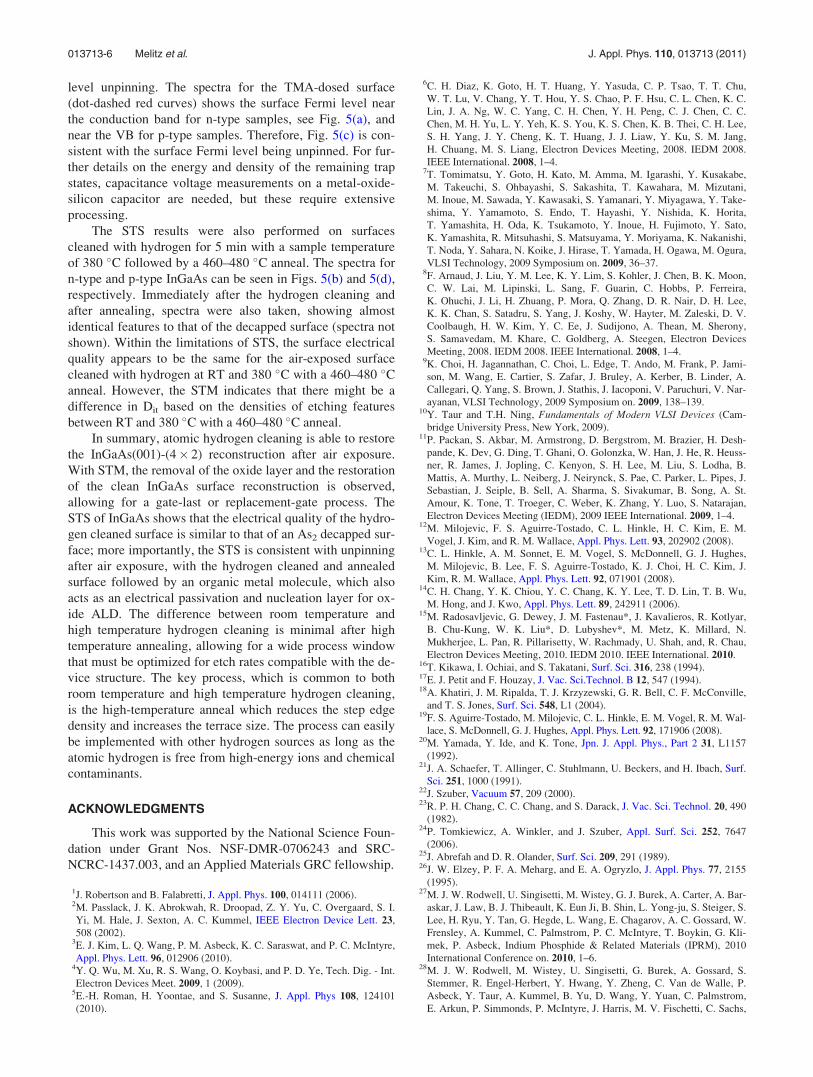
FIG. 4. (Color online) 40� 40 nm2 filled state STM images of surface after
the TMA dose at room temperature and annealed to 250 �C. The inset shows
an expanded view of 7� 7 nm2 indicated by a black square. The surface
shows high ordered horizontal row features (indicated by the white arrow),
consistent with a surface reconstruction. Reproduced with permission
from ECS Trans. 35(4), 175-189 (2011). Copyright VC 2011, The Electro-
chemical Society.
013713-4 Melitz et al. J. Appl. Phys. 110, 013713 (2011)

Typical surfaces after a 30 min air exposure and a 30
min atomic hydrogen cleaning at 380 �C followed by
460–480 �C have 13.9% surface coverage of step edges
[Fig. 4(c)], which is close to that of the decapped surface
consistent with the annealing removing most etching-
induced step formation. The RT hydrogen dosed samples,
even with a high temperature anneal, were not as flat as the
decapped samples with a percent coverage of the edges of
13.4% and 15.4% for 5 and 30 min doses followed by a 460–
480 �C anneal. The role of the sample temperature of the sur-
face morphology indicates that at 380 �C surface mobility is
enhanced, resulting in smoother surfaces; however, at higher
temperatures the etch rate might be increased because the
GaAs (Ref. 26) atomic hydrogen etch rate increases with
temperature.
The atomic hydrogen induced removal of the oxide layer
involves multiple reactions. Atomic hydrogen can reduce
Ga2O3 to Ga2O and H2O,19,20,24 and desorption of Ga2O
occurs at �400 �C on GaAs and InGaAs.20,43 The influence
of atomic hydrogen on In oxides has been assumed to be sim-
ilar to that of Ga oxides.19 Atomic hydrogen has been shown
to convert atomic As and As2O3 into AsH3 and/or H2O.44
Atomic hydrogen on 400 �C samples of GaAs and InGaAs is
known to remove As.19,20 Furthermore, the desorption of As
oxides and As2/As4 occurs around 400 �C.19,20 This hydrogen
induced volatilization of As is consistent with the reduction
of any excess As defects on the hydrogen clean surfaces in
the present study. The absence of any oxides in the present
study is likely due to the > 300 L exposure which reduces
any Ga2O3 or In2O3 to suboxides which are volatilized during
annealing along with any As oxides.
To determine the electrical quality of the InGaAs(001)-
(4� 2) surface, electrical passivation is required because the
decapped surface is pinned.29 Following atomic hydrogen
cleaning, the surface was exposed to TMA at room tempera-
ture and annealed to 250 �C; an STM image of the TMA-
dosed surface can be seen in Fig. 4. The TMA induces a
surface reconstruction, creating a bulklike bonding configu-
ration between the Al atoms and the surface As atoms.38 The
TMA passivation layer has horizontal rows of dimethyl
aluminum. The surface is a highly-ordered self-limiting layer
that has a high nucleation density. The self-limiting and high
nucleation density is necessary for EOT scaling. The STM
image of the TMA-dosed surface shows that this surfaces
satisfies the key processing conditions for gate oxide deposi-
tion: an atomically flat, high nucleation density, and electri-
cally unpinned as shown next by STS.
The STS spectra for n-type and p-type decapped InGaAs
can be seen in Fig. 5. The Normalized dI=dVð Þ= I=Vð Þ spec-
tra is proportional to the local density of states of the sur-
face.45,46 The STS was performed with a modulation
frequency of 1 kHz, a lock-in time constant of 20 ms, and a
T-raster of 40 ms; therefore, it is sensitive to all trap states
with a lifetime less than 1 ms. In the spectra, the zero sample
bias is the Fermi level position of the surface relative to the
bands. For the decapped surface (solid blue curves), the
Fermi level on both the n-type and p-type samples is posi-
tioned near the valence band (VB), indicating that the dec-
apped surface is pinned. After air exposure and hydrogen
cleaning for 5 min at room temperature followed by a 460–
480 �C anneal, the spectra look almost identical to the dec-
apped surface, shown by the blue and green curves in Fig.
5(a) for n-type InGaAs. This is also the case for the p-type at
room temperature (spectra not shown). The STS spectra for
the dark horizontal defects, bright vertical defects, and step
edges were taken (not shown). The STS spectra for the
defects showed a slight change in the relative signal intensity
of the filled and empty states, however, the differences
were not enough to draw any significant conclusions. For
InGaAs(001)-(4� 2), the clean defect-free reconstructed sur-
face is pinned which would make single defect site STS very
difficult because the background signal from the recon-
structed surface would dominate the local signal.
To demonstrate that atomic hydrogen cleaning not only
restores the surface morphology but also the electrical char-
acteristics, TMA is deposited to document the surface Fermi
FIG. 5. (Color online) Normalized dI=dVð Þ= I=Vð Þ spectra using variable-z STS of dec-
apped InGaAs(001)-(4� 2) (solid blue line), 30
min air exposed and hydrogen cleaned for 30
min (dashed green line), and the room tempera-
ture dose of TMA followed by a 250 �C anneal
(dot–dashed red line). Spectra for n-type
InGaAs with hydrogen cleaning at (a) 24 �C,
and (b) 380 �C. Spectra for p-type InGaAs with
hydrogen cleaning at (c) 24 �C, and (d) 380 �C.
Dz for spectra ranges from 0.1–0.3 nm/V. I/V is
smoothed before dI=dVð Þ= I=Vð Þ is calculated
(see Ref. 35). The 0.4 V shift in the VB side of
the dot-dashed red curve for (a) the n-type and
(b) and the absence of a shift in the p-type. (c)
and (d) Indicates an unpinned surface Fermi
level.
013713-5 Melitz et al. J. Appl. Phys. 110, 013713 (2011)
level unpinning. The spectra for the TMA-dosed surface
(dot-dashed red curves) shows the surface Fermi level near
the conduction band for n-type samples, see Fig. 5(a), and
near the VB for p-type samples. Therefore, Fig. 5(c) is con-
sistent with the surface Fermi level being unpinned. For fur-
ther details on the energy and density of the remaining trap
states, capacitance voltage measurements on a metal-oxide-
silicon capacitor are needed, but these require extensive
processing.
The STS results were also performed on surfaces
cleaned with hydrogen for 5 min with a sample temperature
of 380 �C followed by a 460–480 �C anneal. The spectra for
n-type and p-type InGaAs can be seen in Figs. 5(b) and 5(d),
respectively. Immediately after the hydrogen cleaning and
after annealing, spectra were also taken, showing almost
identical features to that of the decapped surface (spectra not
shown). Within the limitations of STS, the surface electrical
quality appears to be the same for the air-exposed surface
cleaned with hydrogen at RT and 380 �C with a 460–480 �Canneal. However, the STM indicates that there might be a
difference in Dit based on the densities of etching features
between RT and 380 �C with a 460–480 �C anneal.
In summary, atomic hydrogen cleaning is able to restore
the InGaAs(001)-(4� 2) reconstruction after air exposure.
With STM, the removal of the oxide layer and the restoration
of the clean InGaAs surface reconstruction is observed,
allowing for a gate-last or replacement-gate process. The
STS of InGaAs shows that the electrical quality of the hydro-
gen cleaned surface is similar to that of an As2 decapped sur-
face; more importantly, the STS is consistent with unpinning
after air exposure, with the hydrogen cleaned and annealed
surface followed by an organic metal molecule, which also
acts as an electrical passivation and nucleation layer for ox-
ide ALD. The difference between room temperature and
high temperature hydrogen cleaning is minimal after high
temperature annealing, allowing for a wide process window
that must be optimized for etch rates compatible with the de-
vice structure. The key process, which is common to both
room temperature and high temperature hydrogen cleaning,
is the high-temperature anneal which reduces the step edge
density and increases the terrace size. The process can easily
be implemented with other hydrogen sources as long as the
atomic hydrogen is free from high-energy ions and chemical
contaminants.
ACKNOWLEDGMENTS
This work was supported by the National Science Foun-
dation under Grant Nos. NSF-DMR-0706243 and SRC-
NCRC-1437.003, and an Applied Materials GRC fellowship.
1J. Robertson and B. Falabretti, J. Appl. Phys. 100, 014111 (2006).2M. Passlack, J. K. Abrokwah, R. Droopad, Z. Y. Yu, C. Overgaard, S. I.
Yi, M. Hale, J. Sexton, A. C. Kummel, IEEE Electron Device Lett. 23,
508 (2002).3E. J. Kim, L. Q. Wang, P. M. Asbeck, K. C. Saraswat, and P. C. McIntyre,
Appl. Phys. Lett. 96, 012906 (2010).4Y. Q. Wu, M. Xu, R. S. Wang, O. Koybasi, and P. D. Ye, Tech. Dig. - Int.
Electron Devices Meet. 2009, 1 (2009).5E.-H. Roman, H. Yoontae, and S. Susanne, J. Appl. Phys 108, 124101
(2010).
6C. H. Diaz, K. Goto, H. T. Huang, Y. Yasuda, C. P. Tsao, T. T. Chu,
W. T. Lu, V. Chang, Y. T. Hou, Y. S. Chao, P. F. Hsu, C. L. Chen, K. C.
Lin, J. A. Ng, W. C. Yang, C. H. Chen, Y. H. Peng, C. J. Chen, C. C.
Chen, M. H. Yu, L. Y. Yeh, K. S. You, K. S. Chen, K. B. Thei, C. H. Lee,
S. H. Yang, J. Y. Cheng, K. T. Huang, J. J. Liaw, Y. Ku, S. M. Jang,
H. Chuang, M. S. Liang, Electron Devices Meeting, 2008. IEDM 2008.
IEEE International. 2008, 1–4.7T. Tomimatsu, Y. Goto, H. Kato, M. Amma, M. Igarashi, Y. Kusakabe,
M. Takeuchi, S. Ohbayashi, S. Sakashita, T. Kawahara, M. Mizutani,
M. Inoue, M. Sawada, Y. Kawasaki, S. Yamanari, Y. Miyagawa, Y. Take-
shima, Y. Yamamoto, S. Endo, T. Hayashi, Y. Nishida, K. Horita,
T. Yamashita, H. Oda, K. Tsukamoto, Y. Inoue, H. Fujimoto, Y. Sato,
K. Yamashita, R. Mitsuhashi, S. Matsuyama, Y. Moriyama, K. Nakanishi,
T. Noda, Y. Sahara, N. Koike, J. Hirase, T. Yamada, H. Ogawa, M. Ogura,
VLSI Technology, 2009 Symposium on. 2009, 36–37.8F. Arnaud, J. Liu, Y. M. Lee, K. Y. Lim, S. Kohler, J. Chen, B. K. Moon,
C. W. Lai, M. Lipinski, L. Sang, F. Guarin, C. Hobbs, P. Ferreira,
K. Ohuchi, J. Li, H. Zhuang, P. Mora, Q. Zhang, D. R. Nair, D. H. Lee,
K. K. Chan, S. Satadru, S. Yang, J. Koshy, W. Hayter, M. Zaleski, D. V.
Coolbaugh, H. W. Kim, Y. C. Ee, J. Sudijono, A. Thean, M. Sherony,
S. Samavedam, M. Khare, C. Goldberg, A. Steegen, Electron Devices
Meeting, 2008. IEDM 2008. IEEE International. 2008, 1–4.9K. Choi, H. Jagannathan, C. Choi, L. Edge, T. Ando, M. Frank, P. Jami-
son, M. Wang, E. Cartier, S. Zafar, J. Bruley, A. Kerber, B. Linder, A.
Callegari, Q. Yang, S. Brown, J. Stathis, J. Iacoponi, V. Paruchuri, V. Nar-
ayanan, VLSI Technology, 2009 Symposium on. 2009, 138–139.10Y. Taur and T.H. Ning, Fundamentals of Modern VLSI Devices (Cam-
bridge University Press, New York, 2009).11P. Packan, S. Akbar, M. Armstrong, D. Bergstrom, M. Brazier, H. Desh-
pande, K. Dev, G. Ding, T. Ghani, O. Golonzka, W. Han, J. He, R. Heuss-
ner, R. James, J. Jopling, C. Kenyon, S. H. Lee, M. Liu, S. Lodha, B.
Mattis, A. Murthy, L. Neiberg, J. Neirynck, S. Pae, C. Parker, L. Pipes, J.
Sebastian, J. Seiple, B. Sell, A. Sharma, S. Sivakumar, B. Song, A. St.
Amour, K. Tone, T. Troeger, C. Weber, K. Zhang, Y. Luo, S. Natarajan,
Electron Devices Meeting (IEDM), 2009 IEEE International. 2009, 1–4.12M. Milojevic, F. S. Aguirre-Tostado, C. L. Hinkle, H. C. Kim, E. M.
Vogel, J. Kim, and R. M. Wallace, Appl. Phys. Lett. 93, 202902 (2008).13C. L. Hinkle, A. M. Sonnet, E. M. Vogel, S. McDonnell, G. J. Hughes,
M. Milojevic, B. Lee, F. S. Aguirre-Tostado, K. J. Choi, H. C. Kim, J.
Kim, R. M. Wallace, Appl. Phys. Lett. 92, 071901 (2008).14C. H. Chang, Y. K. Chiou, Y. C. Chang, K. Y. Lee, T. D. Lin, T. B. Wu,
M. Hong, and J. Kwo, Appl. Phys. Lett. 89, 242911 (2006).15M. Radosavljevic, G. Dewey, J. M. Fastenau*, J. Kavalieros, R. Kotlyar,
B. Chu-Kung, W. K. Liu*, D. Lubyshev*, M. Metz, K. Millard, N.
Mukherjee, L. Pan, R. Pillarisetty, W. Rachmady, U. Shah, and, R. Chau,
Electron Devices Meeting, 2010. IEDM 2010. IEEE International. 2010.16T. Kikawa, I. Ochiai, and S. Takatani, Surf. Sci. 316, 238 (1994).17E. J. Petit and F. Houzay, J. Vac. Sci.Technol. B 12, 547 (1994).18A. Khatiri, J. M. Ripalda, T. J. Krzyzewski, G. R. Bell, C. F. McConville,
and T. S. Jones, Surf. Sci. 548, L1 (2004).19F. S. Aguirre-Tostado, M. Milojevic, C. L. Hinkle, E. M. Vogel, R. M. Wal-
lace, S. McDonnell, G. J. Hughes, Appl. Phys. Lett. 92, 171906 (2008).20M. Yamada, Y. Ide, and K. Tone, Jpn. J. Appl. Phys., Part 2 31, L1157
(1992).21J. A. Schaefer, T. Allinger, C. Stuhlmann, U. Beckers, and H. Ibach, Surf.
Sci. 251, 1000 (1991).22J. Szuber, Vacuum 57, 209 (2000).23R. P. H. Chang, C. C. Chang, and S. Darack, J. Vac. Sci. Technol. 20, 490
(1982).24P. Tomkiewicz, A. Winkler, and J. Szuber, Appl. Surf. Sci. 252, 7647
(2006).25J. Abrefah and D. R. Olander, Surf. Sci. 209, 291 (1989).26J. W. Elzey, P. F. A. Meharg, and E. A. Ogryzlo, J. Appl. Phys. 77, 2155
(1995).27M. J. W. Rodwell, U. Singisetti, M. Wistey, G. J. Burek, A. Carter, A. Bar-
askar, J. Law, B. J. Thibeault, K. Eun Ji, B. Shin, L. Yong-ju, S. Steiger, S.
Lee, H. Ryu, Y. Tan, G. Hegde, L. Wang, E. Chagarov, A. C. Gossard, W.
Frensley, A. Kummel, C. Palmstrom, P. C. McIntyre, T. Boykin, G. Kli-
mek, P. Asbeck, Indium Phosphide & Related Materials (IPRM), 2010
International Conference on. 2010, 1–6.28M. J. W. Rodwell, M. Wistey, U. Singisetti, G. Burek, A. Gossard, S.
Stemmer, R. Engel-Herbert, Y. Hwang, Y. Zheng, C. Van de Walle, P.
Asbeck, Y. Taur, A. Kummel, B. Yu, D. Wang, Y. Yuan, C. Palmstrom,
E. Arkun, P. Simmonds, P. McIntyre, J. Harris, M. V. Fischetti, C. Sachs,
013713-6 Melitz et al. J. Appl. Phys. 110, 013713 (2011)

Indium Phosphide and Related Materials, 2008. IPRM 2008. 20th Interna-
tional Conference on. 2008, 1–6.29W. Melitz, J. Shen, S. Lee, J. S. Lee, A. C. Kummel, R. Droopad, E. T.
Yu, J. Appl. Phys. 108, 023711 (2010).30M. Yokoyama, T. Yasuda, H. Takagi, H. Yamada, N. Fukuhara, M. Hata,
M. Sugiyama, Y. Nakano, M. Takenaka, and S. Takagi, Appl. Phys.
Express 2, 124501 (2009).31S. J. Pearton, F. Ren, C. R. Abernathy, W. S. Hobson, T. R. Fullowan, R.
Esagui, and J. R. Lothian, Appl. Phys. Lett. 61, 586 (1992).32R. M. Feenstra, Surf. Sci. 300, 965 (1994).33J. A. Stroscio, R. M. Feenstra, D.M. Newns, and A. P. Fein, J. Vac. Sci.
Technol. A 6, 499 (1988).34W. Monch, Semiconductor Surfaces and Interfaces (Springer-Verlag, Ber-
lin, 2009).35P. Martensson and R. M. Feenstra, Phys. Rev. B 39, 7744 (1989).36J. Shen, J. B. Clemens, E. A. Chagarov, D. L. Feldwinn, W. Melitz, T. Song,
S. R. Bishop, A. C. Kummel, and R. Droopad, Surf. Sci. 604, 1757 (2010).
37J. Shen, D. L. Winn, W. Melitz, J. B. Clemens, and A. C. Kummel, ECS
Trans. 16, 463 (2008).38J. B. Clemens, E. A. Chagarov, M. Holland, R. Droopad, J. A. Shen, and
A. C. Kummel, J. Chem. Phys. 133, 154704 (2010).39M. M. Sung and J.W. Rabalais, Surf. Sci. 356, 161 (1996).40N. Ikoma and S. Ohkouchi, Jpn. J Appl. Phys., Part 1 34, 5763 (1995).41Y. Horikoshi, H. Yamaguchi, F. Briones, and M. Kawashima, J. Cryst.
Growth 105, 326 (1990).42Y. Horikoshi, M. Kawashima, and H. Yamaguchi, Appl. Phys. Lett. 50,
1686 (1987).43M. Yamada, Jpn. J. Appl. Phys., Part 2 35, L651 (1996).44S. J. Pearton, Mater. Sci. Eng., B 10, 187 (1991).45R. J. Hamers and D. F. Padowitz, “Methods of Tunneling Spectroscopy
with the STM,” in Scanning Probe Microscopy and Spectroscopy: Theory,Techniques, and Applications, 2nd ed. (Wiley-VCH, New York, 2001).
46C. J. Chen, Introduction to Scanning Tunneling Microscopy (Oxford Uni-
versity Press, New York, 1993).
013713-7 Melitz et al. J. Appl. Phys. 110, 013713 (2011)