Embed Size (px)
Citation preview
04/19/23Based on text by S. Mourad
"Priciples of Electronic Systems"
Digital Testing: Testability Measures
Fab. 2, 2001 Copyrights(c) 2001, Samiha Mourad 2
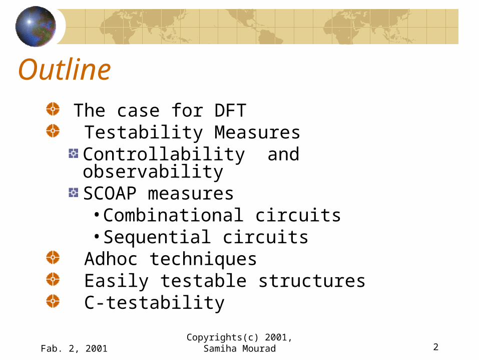
Outline The case for DFT Testability Measures
Controllability and observabilitySCOAP measures• Combinational circuits• Sequential circuits
Adhoc techniques Easily testable structures C-testability
What is Design for Test ?
Also called design for testability
That is design to facilitate testing No formal definition for testability Possible definition, testability increases as the cost and time of testing decreases
The Case for DFT High device density
Large number of gates per pin• see next chart
High cost of ATPG particularly for sequential circuits
Need for a shorter design & test cycle• shorter-time-to-market
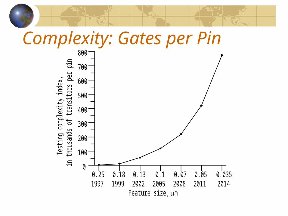
Complexity: Gates per Pin800
700
600
500
400
300
200
100
00.251997
0.181999
0.132002
0.12005
0.072008
0.052011
0.0352014
Testi
ng c
ompl
exity
inde
x,in
thou
sand
s of t
rans
itors
per
pin
Feature size, m
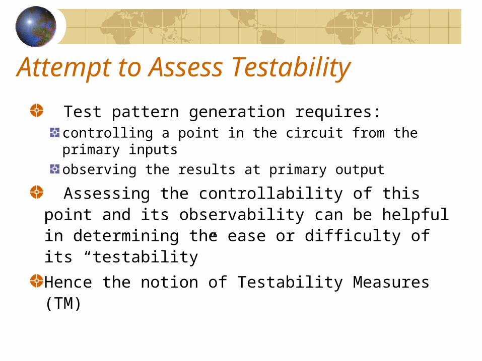
Attempt to Assess Testability
Test pattern generation requires:controlling a point in the circuit from the primary inputsobserving the results at primary output
Assessing the controllability of this point and its observability can be helpful in determining the ease or difficulty of its “testability”
Hence the notion of Testability Measures (TM)
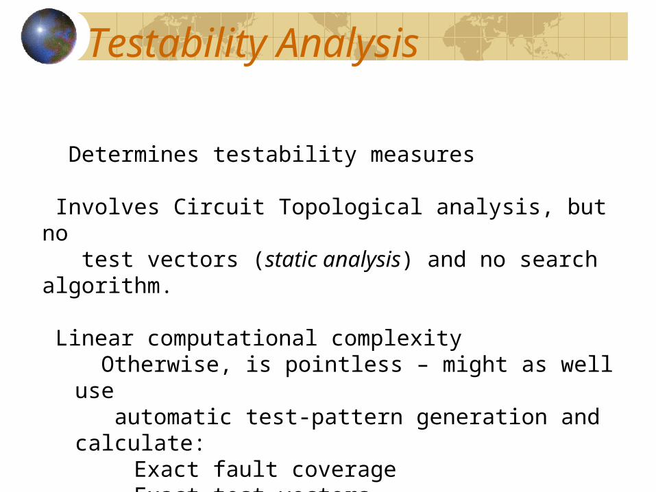
Testability Analysis
Determines testability measures Involves Circuit Topological analysis, but no test vectors (static analysis) and no search algorithm.
Linear computational complexity Otherwise, is pointless – might as well use automatic test-pattern generation and calculate:
Exact fault coverage Exact test vectors
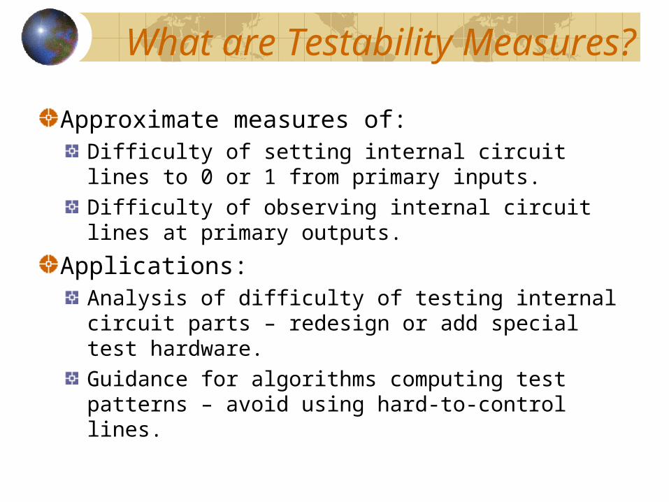
What are Testability Measures?
Approximate measures of:Difficulty of setting internal circuit lines to 0 or 1 from primary inputs.
Difficulty of observing internal circuit lines at primary outputs.
Applications:Analysis of difficulty of testing internal circuit parts – redesign or add special test hardware.
Guidance for algorithms computing test patterns – avoid using hard-to-control lines.
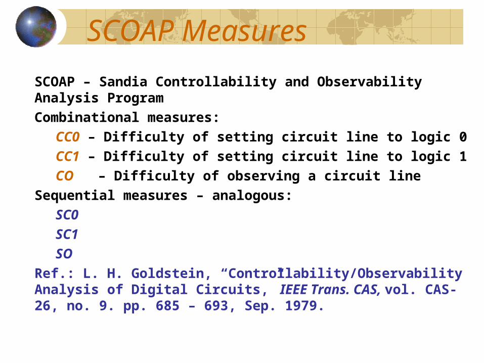
SCOAP Measures
SCOAP – Sandia Controllability and Observability Analysis Program
Combinational measures: CC0 – Difficulty of setting circuit line to logic 0 CC1 – Difficulty of setting circuit line to logic 1 CO – Difficulty of observing a circuit line
Sequential measures – analogous: SC0 SC1 SO
Ref.: L. H. Goldstein, “Controllability/Observability Analysis of Digital Circuits,” IEEE Trans. CAS, vol. CAS-26, no. 9. pp. 685 – 693, Sep. 1979.
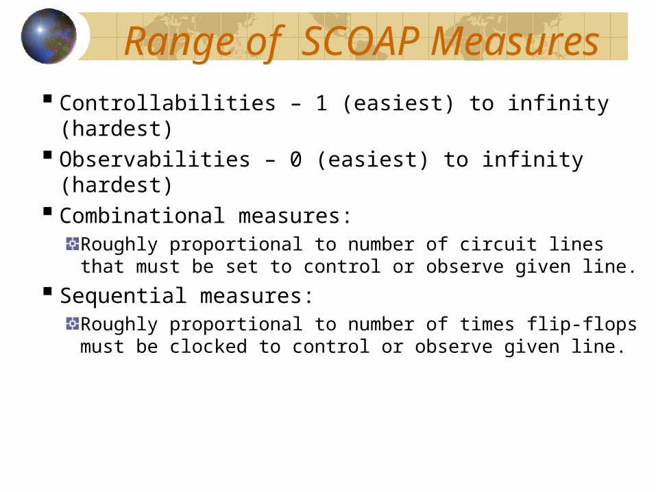
Range of SCOAP Measures
Controllabilities – 1 (easiest) to infinity (hardest) Observabilities – 0 (easiest) to infinity (hardest) Combinational measures:
Roughly proportional to number of circuit lines that must be set to control or observe given line.
Sequential measures:Roughly proportional to number of times flip-flops must be clocked to control or observe given line.
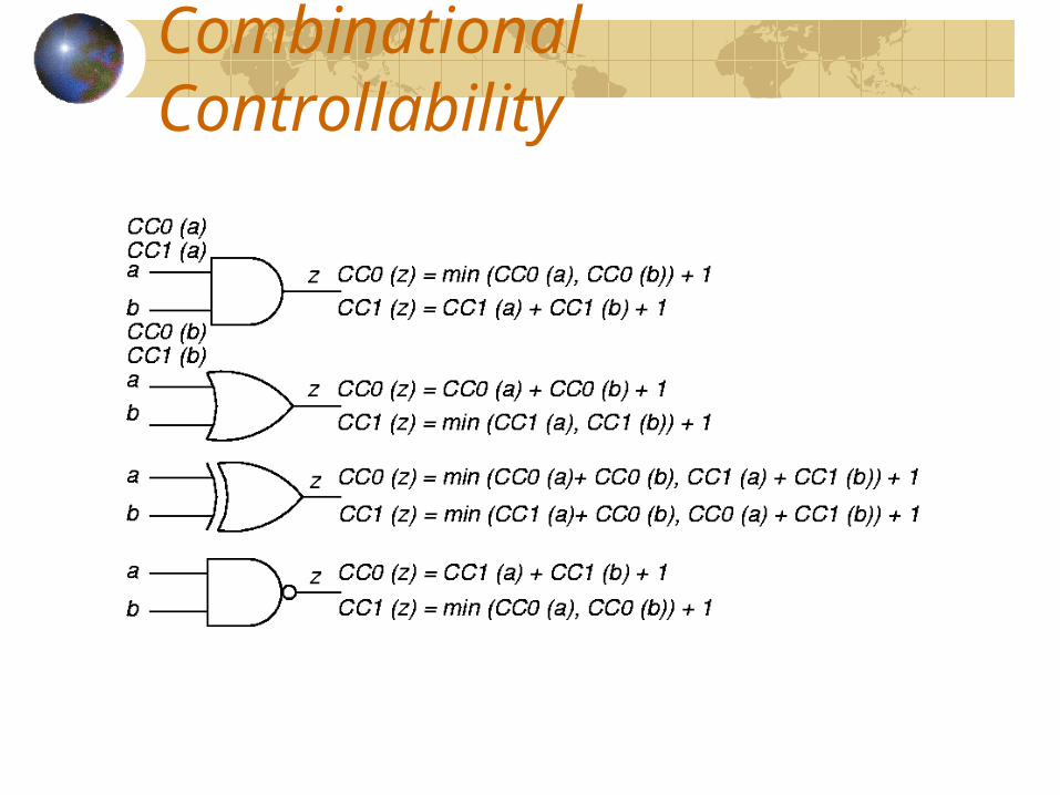
Combinational Controllability
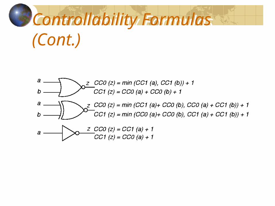
Controllability Formulas (Cont.)Controllability Formulas (Cont.)
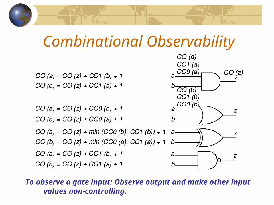
Combinational ObservabilityCombinational Observability
To observe a gate input: Observe output and make other input values non-controlling.
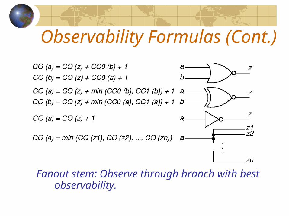
Observability Formulas (Cont.)Observability Formulas (Cont.)
Fanout stem: Observe through branch with best observability.
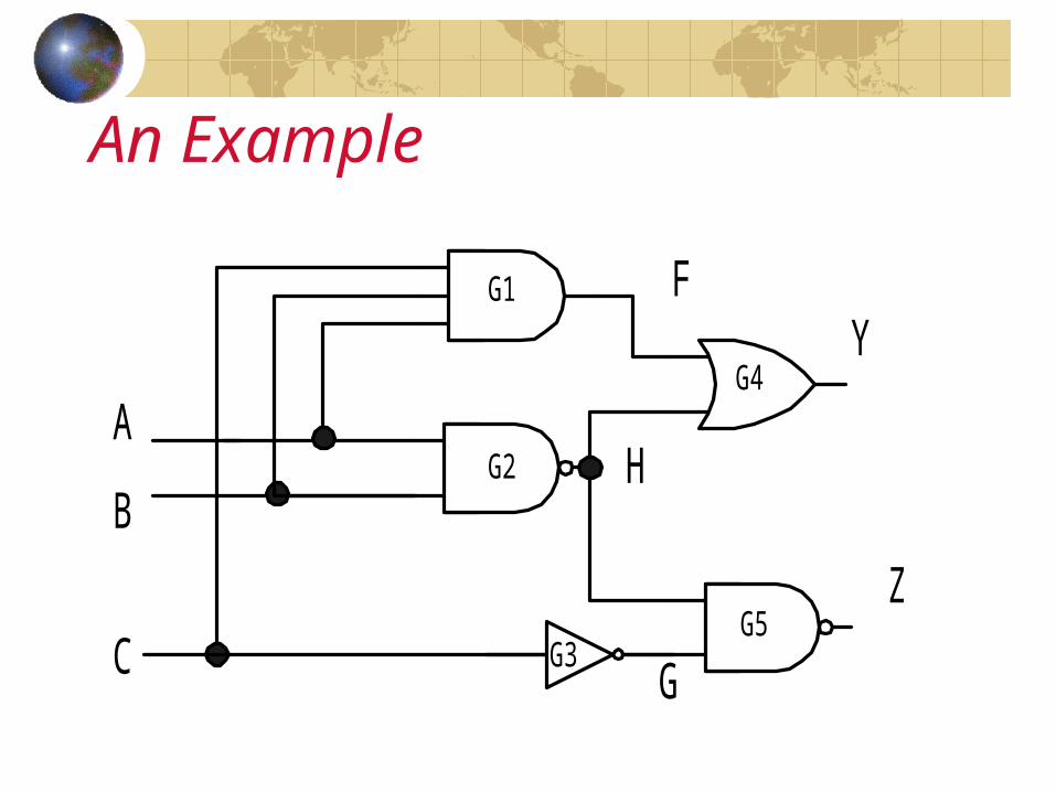
An Example
Z
Y
A
B
C
G1
G2
G3
G4
G5
F
H
G
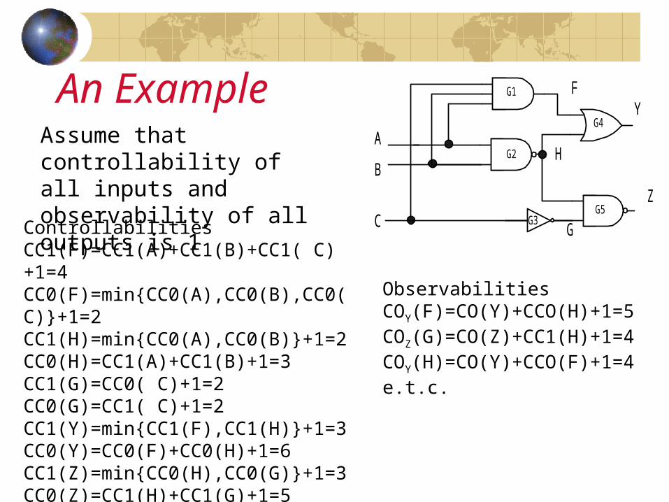
An Example
Z
Y
A
B
C
G1
G2
G3
G4
G5
F
H
GControllabilitiesCC1(F)=CC1(A)+CC1(B)+CC1( C)+1=4CC0(F)=min{CC0(A),CC0(B),CC0( C)}+1=2CC1(H)=min{CC0(A),CC0(B)}+1=2CC0(H)=CC1(A)+CC1(B)+1=3CC1(G)=CC0( C)+1=2CC0(G)=CC1( C)+1=2CC1(Y)=min{CC1(F),CC1(H)}+1=3CC0(Y)=CC0(F)+CC0(H)+1=6CC1(Z)=min{CC0(H),CC0(G)}+1=3CC0(Z)=CC1(H)+CC1(G)+1=5
Assume that controllability of all inputs and observability of all outputs is 1
ObservabilitiesCOY(F)=CO(Y)+CCO(H)+1=5COZ(G)=CO(Z)+CC1(H)+1=4COY(H)=CO(Y)+CCO(F)+1=4e.t.c.
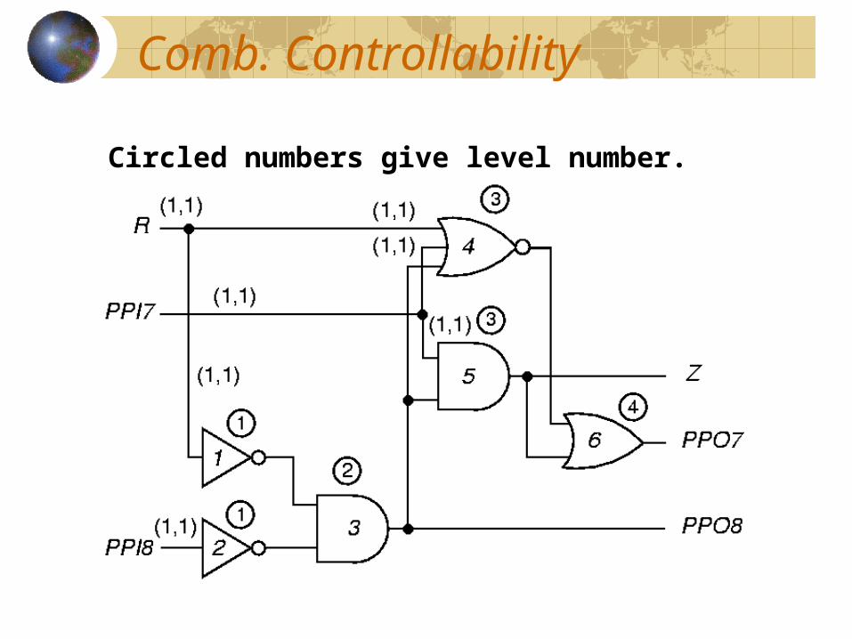
Comb. Controllability
Circled numbers give level number. (CC0, CC1)
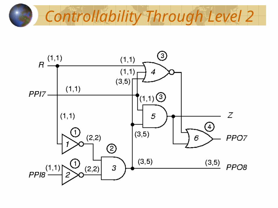
Controllability Through Level 2
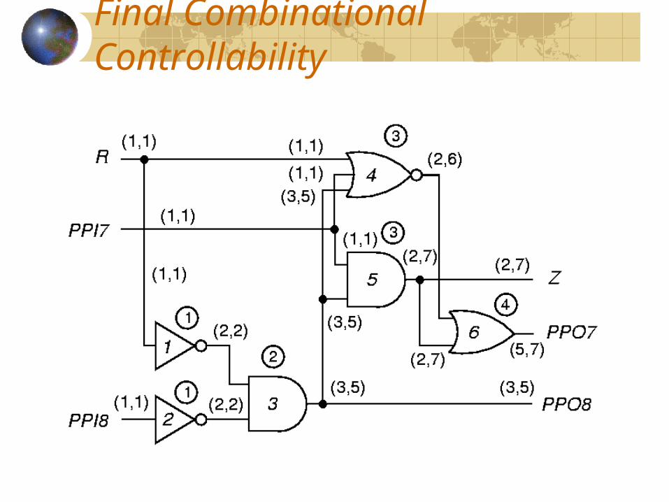
Final Combinational Controllability
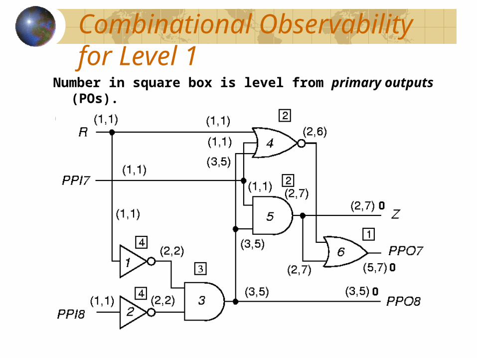
Combinational Observability for Level 1
Number in square box is level from primary outputs (POs).
(CC0, CC1) CO
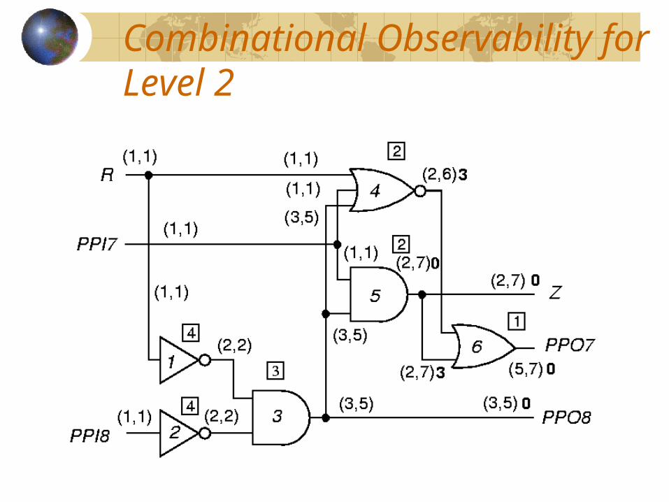
Combinational Observability for Level 2
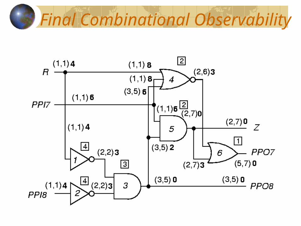
Final Combinational Observability
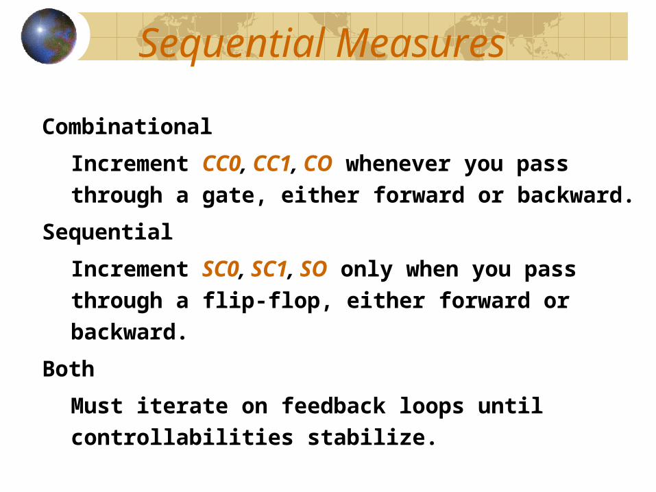
Sequential Measures
Combinational
Increment CC0, CC1, CO whenever you pass through
a gate, either forward or backward.
Sequential
Increment SC0, SC1, SO only when you pass through
a flip-flop, either forward or backward.
Both
Must iterate on feedback loops until controllabilities
stabilize.
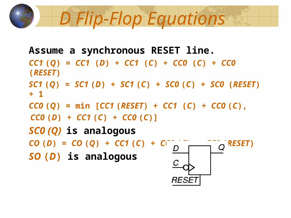
D Flip-Flop Equations
Assume a synchronous RESET line. CC1 (Q) = CC1 (D) + CC1 (C) + CC0 (C) + CC0 (RESET) SC1 (Q) = SC1 (D) + SC1 (C) + SC0 (C) + SC0 (RESET) + 1 CC0 (Q) = min [CC1 (RESET) + CC1 (C) + CC0 (C),
CC0 (D) + CC1 (C) + CC0 (C)]
SC0 (Q) is analogous CO (D) = CO (Q) + CC1 (C) + CC0 (C) + CC0 (RESET)
SO (D) is analogous
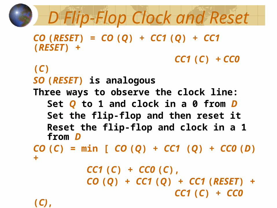
D Flip-Flop Clock and Reset CO (RESET) = CO (Q) + CC1 (Q) + CC1 (RESET) + CC1 (C) + CC0 (C) SO (RESET) is analogous Three ways to observe the clock line:
1. Set Q to 1 and clock in a 0 from D2. Set the flip-flop and then reset it3. Reset the flip-flop and clock in a 1 from D
CO (C) = min [ CO (Q) + CC1 (Q) + CC0 (D) + CC1 (C) + CC0 (C), CO (Q) + CC1 (Q) + CC1 (RESET) + CC1 (C) + CC0 (C), CO (Q) + CC0 (Q) + CC0 (RESET) + CC1 (D) + CC1 (C) + CC0 (C)] SO (C) is analogous
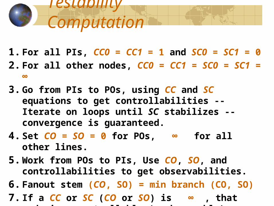
Testability Computation
1. For all PIs, CC0 = CC1 = 1 and SC0 = SC1 = 0
2. For all other nodes, CC0 = CC1 = SC0 = SC1 = ∞3. Go from PIs to POs, using CC and SC equations to get
controllabilities -- Iterate on loops until SC stabilizes -- convergence is guaranteed.
4. Set CO = SO = 0 for POs, ∞ for all other lines.
5. Work from POs to PIs, Use CO, SO, and controllabilities to get observabilities.
6. Fanout stem (CO, SO) = min branch (CO, SO)
7. If a CC or SC (CO or SO) is ∞ , that node is uncontrollable (unobservable).
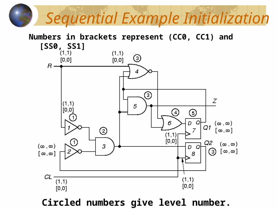
Sequential Example Initialization
Circled numbers give level number. (CC0, CC1)
Numbers in brackets represent (CC0, CC1) and [SS0, SS1]
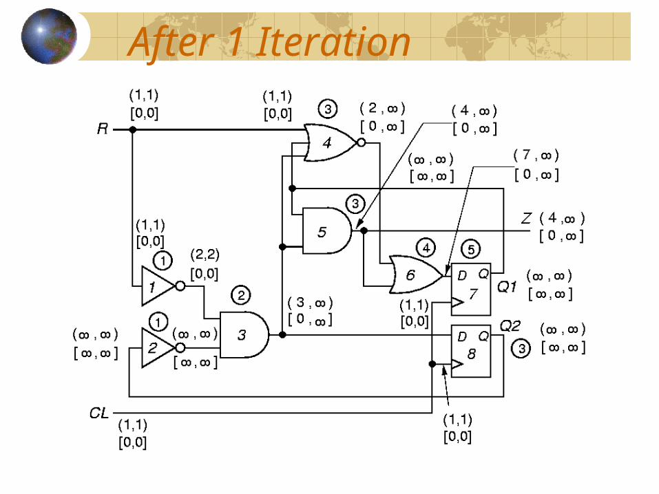
After 1 Iteration
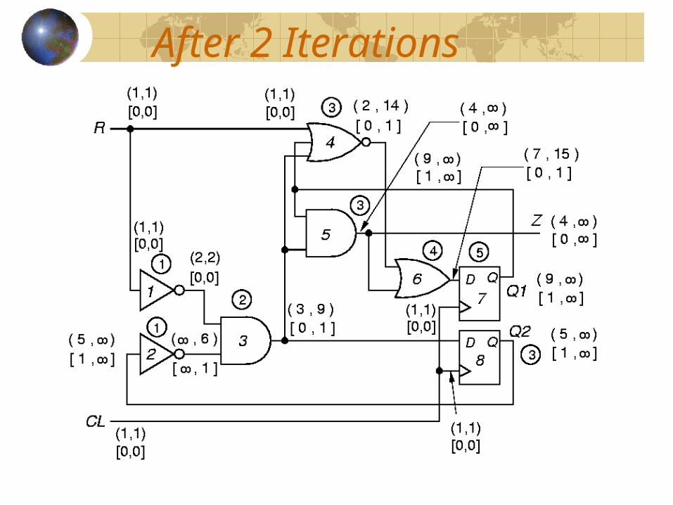
After 2 Iterations
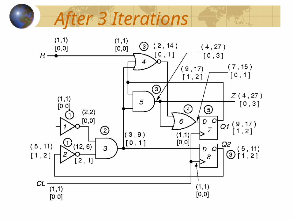
After 3 Iterations
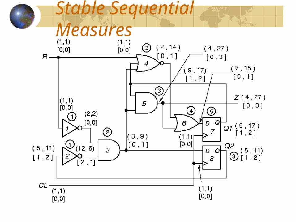
Stable Sequential Measures
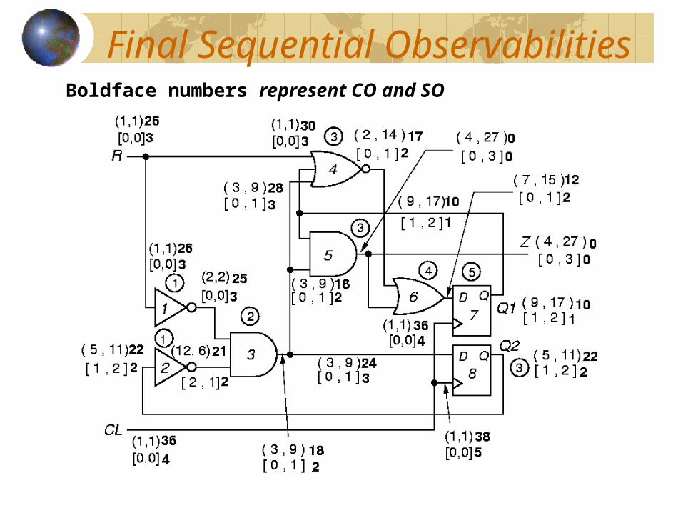
Final Sequential ObservabilitiesBoldface numbers represent CO and SO
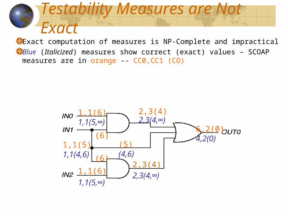
Testability Measures are Not Exact
Exact computation of measures is NP-Complete and impractical
Blue (Italicized) measures show correct (exact) values – SCOAP measures are in orange -- CC0,CC1 (CO)
1,1(6)1,1(5,∞)
1,1(5)1,1(4,6)
1,1(6)
1,1(5,∞)
6,2(0)4,2(0)
2,3(4)2,3(4,∞)
(5)(4,6)(6)
(6)
2,3(4)2,3(4,∞)
SummarySummary
Testability measures are approximate measures of:Difficulty of setting circuit lines to 0 or 1
Difficulty of observing internal circuit lines
Applications:Analysis of difficulty of testing internal circuit parts
• Redesign circuit hardware or add special test hardware where measures show poor controllability or observability.
Guidance for algorithms computing test patterns – avoid using hard-to-control lines
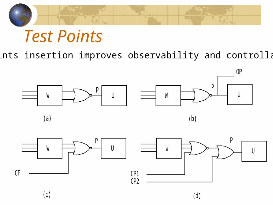
Test Points
CP1CP2
CP
P
(a) (b)
(c) (d)
OP
PP
PU
W U
UWW
UW
Test points insertion improves observability and controllability
CAD Tools
All aspect of ASIC design and test depends on CAD tools CAD programs perform different tasks:
Design entry, Simulation, Synthesis, layout, Test pattern generation, Fault grading, Floor planning, Technology mapping, Place and route, DRC, LVS, Parameter extraction
Most these problems are NP-complete There is a need for algorithms that utilize some heuristic and a cost function to stop the computation.
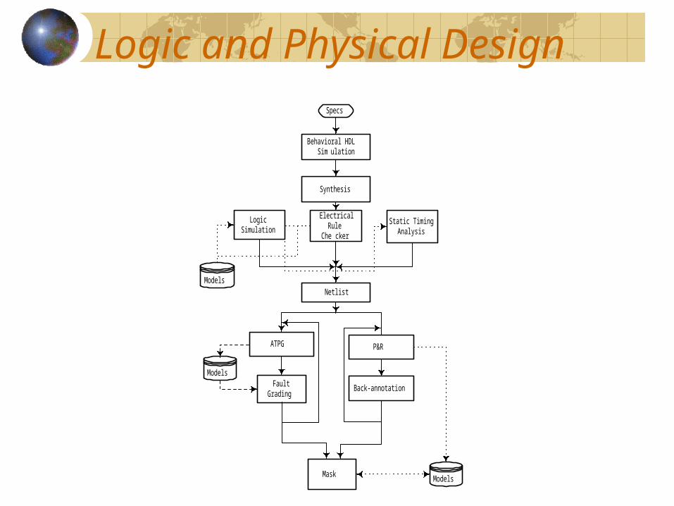
Logic and Physical DesignSpecs
Behavioral HDLSim ulation
Static TimingAnalysis
ElectricalRule
Che cker
LogicSimulation
Synthesis
ModelsNetlist
ATPG
FaultGrading
P&R
Models
Back-annotation
Mask Models