Embed Size (px)
Citation preview

10-Bit, 65/80/105 MSPS,3 V A/D Converter
Data Sheet AD9215
Rev. B Document Feedback Information furnished by Analog Devices is believed to be accurate and reliable. However, no re-sponsibility is assumed by Analog Devices for its use, nor for any infringements of patents or other rights of third parties that may result from its use. Specifications subject to change without notice. No license is granted by implication or otherwise under any patent or patent rights of Analog Devices. Trademarks and registered trademarks are the property of their respective owners.
One Technology Way, P.O. Box 9106, Norwood, MA 02062-9106, U.S.A. Tel: 781.329.4700 ©2003–2013 Analog Devices, Inc. All rights reserved. Technical Support www.analog.com
FEATURES
Single 3 V supply operation (2.7 V to 3.3 V) SNR = 58 dBc (to Nyquist) SFDR = 77 dBc (to Nyquist) Low power ADC core: 96 mW at 65 MSPS, 104 mW
@ 80 MSPS, 120 mW at 105 MSPS Differential input with 300 MHz bandwidth On-chip reference and sample-and-hold amplifier DNL = ±0.25 LSB Flexible analog input: 1 V p-p to 2 V p-p range Offset binary or twos complement data format Clock duty cycle stabilizer
APPLICATIONS
Ultrasound equipment IF sampling in communications receivers Battery-powered instruments Hand-held scopemeters Low cost digital oscilloscopes
FUNCTIONAL BLOCK DIAGRAM
SHAVIN+
VIN–
REFT
REFB
DRVDD
CLK PDWN MODE
CLOCKDUTY CYCLESTABLIZER
MODESELECT
DGND
OR
D9 (MSB)
0287
4-A
-001
D0
AVDD
CORRECTION LOGIC
OUTPUT BUFFERS
10
REFSELECT
AGND
0.5V
VREF
SENSE
AD9215
PIPELINEADC CORE
Figure 1.
PRODUCT DESCRIPTION
The AD9215 is a family of monolithic, single 3 V supply, 10-bit, 65/80/105 MSPS analog-to-digital converters (ADC). This family features a high performance sample-and-hold amplifier (SHA) and voltage reference. The AD9215 uses a multistage differential pipelined architecture with output error correction logic to pro-vide 10-bit accuracy at 105 MSPS data rates and to guarantee no missing codes over the full operating temperature range.
The wide bandwidth, truly differential sample-and-hold ampli-fier (SHA) allows for a variety of user-selectable input ranges and offsets including single-ended applications. It is suitable for multiplexed systems that switch full-scale voltage levels in successive channels and for sampling single-channel inputs at frequencies well beyond the Nyquist rate. Combined with pow-er and cost savings over previously available ADCs, the AD9215 is suitable for applications in communications, imaging, and medical ultrasound.
A single-ended clock input is used to control all internal conversion cycles. A duty cycle stabilizer compensates for wide variations in the clock duty cycle while maintaining excellent performance. The digital output data is presented in straight binary or twos complement for-mats. An out-of-range signal indicates an overflow condition, which can be used with the MSB to determine low or high overflow.
Fabricated on an advanced CMOS process, the AD9215 is avail-able in both a 28-lead surface-mount plastic package and a 32-lead chip scale package and is specified over the industrial temperature range of −40°C to +85°C.
PRODUCT HIGHLIGHTS
1. The AD9215 operates from a single 3 V power supply and features a separate digital output driver supply to accom-modate 2.5 V and 3.3 V logic families.
2. Operating at 105 MSPS, the AD9215 core ADC consumes a low 120 mW; at 80 MSPS, the power dissipation is 104 mW; and at 65 MSPS, the power dissipation is 96 mW.
3. The patented SHA input maintains excellent performance for input frequencies up to 200 MHz and can be config-ured for single-ended or differential operation.
4. The AD9215 is part of several pin compatible 10-, 12-, and 14-bit low power ADCs. This allows a simplified upgrade from 10 bits to 12 bits for systems up to 80 MSPS.
5. The clock duty cycle stabilizer maintains converter per-formance over a wide range of clock pulse widths.
6. The out of range (OR) output bit indicates when the signal is beyond the selected input range.

AD9215 Data Sheet
Rev. B | Page 2 of 36
TABLE OF CONTENTS Specifications ..................................................................................... 3
Absolute Maximum Ratings1 .......................................................... 6
Explanation of Test Levels ........................................................... 6
ESD Caution .................................................................................. 6
Pin Configurations and Function Descriptions ........................... 7
Equivalent Circuits ....................................................................... 8
Definitions of Specifications ....................................................... 8
Typical Performance Characteristics ........................................... 10
Applying the AD9215 Theory of Operation ............................... 14
Clock Input and Considerations .............................................. 15
Evaluation Board ........................................................................ 18
Outline Dimensions ....................................................................... 33
Ordering Guide ........................................................................... 34
REVISION HISTORY
2/13—Data Sheet Changed from a REV. A to a REV. B
Changes to Figure 4 and Added EPAD Note to Pin Configura-tions and Function Descriptions Section ..................................... 7
Changes to Voltage Reference Section ........................................ 17
Changes to Evaluation Board Section......................................... 18
Updated Outline Dimensions ...................................................... 33
Changes to Ordering Guide ......................................................... 34
2/04—Data Sheet Changed from a REV. 0 to a REV. A
Renumbered Figures and Tables ..............................UNIVERSAL
Changes to Product Title ................................................................ 1
Changes to Features ........................................................................ 1
Changes to Product Description ................................................... 1
Changes to Product Highlights ..................................................... 1
Changes to Specifications ............................................................... 2
Changes to Figure 2 ......................................................................... 4
Changes to Figures 9 to 11 ........................................................... 10
Added Figure 14 ............................................................................ 10
Added Figures 16 and 18 .............................................................. 11
Changes to Figures 21 to 24 and 25 to 26 ................................... 12
Deleted Figure 25 ........................................................................... 12
Changes to Figures 28 and 29 ...................................................... 13
Changes to Figure 31 ..................................................................... 14
Changes t0 Figure 35 ..................................................................... 16
Changes to Figures 50 through 58............................................... 26
Added Table 11 .............................................................................. 31
Updated Outline Dimensions ...................................................... 32
Changes to Ordering Guide ......................................................... 33
5/03—Revision 0: Initial Version

Data Sheet AD9215
Rev. B | Page 3 of 36
SPECIFICATIONS AVDD = 3 V, DRVDD = 2.5 V, specified maximum conversion rate, 2 V p-p differential input, 1.0 V internal reference, unless otherwise noted.
Table 1. DC Specifications AD9215BRU-65/
AD9215BCP-65 AD9215BRU-80/ AD9215BCP-80
AD9215BRU-105/ AD9215BCP-105
Parameter
Temp
Test Level
Min
Typ
Max
Min
Typ
Max
Min
Typ
Max
Unit
RESOLUTION Full VI 10 10 10 Bits
ACCURACY No Missing Codes Full VI Guaranteed Guaranteed Guaranteed Offset Error1 Full VI ±0.3 ±2.0 ±0.3 ±2.0 ±0.3 ±2.0 % FSR Gain Error1 Full VI 0 +1.5 +4.0 +1.5 +4.0 +1.5 +4.0 % FSR Differential Nonlinearity (DNL)2 Full VI −1.0 ±0.5 +1.0 −1.0 ±0.5 +1.0 −1.0 ±0.6 +1.2 LSB Integral Nonlinearity (INL)2 Full VI ±0.5 ±1.2 ±0.5 ±1.2 ±0.65 ±1.2 LSB
TEMPERATURE DRIFT Offset Error1 Full V +15 +15 +15 ppm/°C Gain Error1 Full V +30 +30 +30 ppm/°C Reference Voltage (1 V Mode) Full V ±230 ±230 ±230 ppm/°C
INTERNAL VOLTAGE REFERENCE Output Voltage Error (1 V Mode) Full VI ±2 ±35 ±2 ±35 ±2 ±35 mV Load Regulation @ 1.0 mA Full V 0.2 0.2 0.2 mV Output Voltage Error (0.5 V Mode) Full V ± 1 ±1 ±1 mV Load Regulation @ 0.5 mA Full V 0.2 0.2 0.2 mV
INPUT REFERRED NOISE VREF = 0.5 V 25°C V 0.8 0.8 0.8 LSB rms VREF = 1.0 V 25°C V 0.4 0.4 0.4 LSB rms
ANALOG INPUT Input Span, VREF = 0.5 V Full IV 1 1 1 V p-p Input Span, VREF = 1.0 V Full IV 2 2 2 V p-p Input Capacitance3 Full V 2 2 2 pF
REFERENCE INPUT RESISTANCE Full V 7 7 7 kΩ
POWER SUPPLIES Supply Voltage
AVDD Full IV 2.7 3.0 3.3 2.7 3.0 3.3 2.7 3.0 3.3 V DRVDD Full IV 2.25 2.5 3.6 2.25 2.5 3.6 2.25 2.5 3.6 V
Supply Current IAVDD
2 Full VI 32 35 34.5 39 40 44 mA IDRVDD
2 25°C V 7.0 8.6 11.3 mA PSRR Full V ± 0.1 ± 0.1 ± 0.1 % FSR
POWER CONSUMPTION Sine Wave Input2
IAVDD2 Full VI 96 104 120 mW
IDRVDD2 25°C V 18 20 25 mW
Standby Power4 25°C V 1.0 1.0 1.0 mW
1 With a 1.0 V internal reference. 2 Measured at fIN = 2.4 MHz, full-scale sine wave, with approximately 5 pF loading on each output bit. 3 Input capacitance refers to the effective capacitance between one differential input pin and AGND. Refer to Figure 5 for the equivalent analog input structure. 4 Standby power is measured with a dc input, the CLK pin inactive (i.e., set to AVDD or AGND).

AD9215 Data Sheet
Rev. B | Page 4 of 36
AVDD = 3 V, DRVDD = 2.5 V, specified maximum conversion rate, 2 V p-p differential input, 1.0 V internal reference, AIN = −0.5 dBFS, MODE = AVDD/3 (duty cycle stabilizer [DCS] enabled), unless otherwise noted.
Table 2. AC Specifications AD9215BRU-65/
AD9215BCP-65 AD9215BRU-80/ AD9215BCP-80
AD9215BRU-105/AD9215BCP-105
Parameter
Temp
Test Level
Min
Typ
Max
Min
Typ
Max
Min
Typ
Max
Unit
SIGNAL-TO-NOISE RATIO (SNR) fIN = 2.4 MHz Full VI 56.0 58.5 56.0 58.5 57.5 dB 25°C I 57.0 59.0 57.0 59.0 56.6 58.5 dB fIN = Nyquist1 Full VI 56.0 58.0 56.0 58.0 57.5 dB 25°C I 56.5 58.5 56.5 58.5 56.4 58.0 dB fIN = 70 MHz 25°C V 58.0 57.8 dB fIN = 100 MHz 25°C V 57.5 57.7 dB
SIGNAL-TO-NOISE AND DISTORTION (SINAD) fIN = 2.4 MHz Full VI 55.8 58.5 55.7 58.5 57.6 dB 25°C I 56.5 59.0 56.8 58.5 56.5 58.2 dB fIN = Nyquist1 Full VI 55.8 58.0 55.5 58.0 57.3 dB 25°C I 56.3 58.5 56.3 58.5 56.1 57.8 dB fIN = 70 MHz 25°C V 56.0 57.7 dB fIN = 100 MHz 25°C V 55.5 57.4 dB
EFFECTIVE NUMBER OF BITS (ENOB) fIN = 2.4 MHz Full VI 9.1 9.5 9.0 9.5 9.3 Bits 25°C I 9.2 9.6 9.3 9.5 9.2 9.5 Bits fIN = Nyquist1 Full VI 9.1 9.4 9.0 9.4 9.4 Bits 25°C I 9.1 9.5 9.0 9.5 9.1 9.4 Bits fIN = 70 MHz 25°C V 9.1 9.4 Bits fIN = 100 MHz 25°C V 9.0 9.3 Bits
WORST HARMONIC (Second or Third) fIN = 2.4 MHz Full VI −78 −64 −78 −64 −78 dBc 25°C I −80 −65 −80 −65 −84 −70 dBc fIN = Nyquist1 Full VI −77 −64 −76 −63 −74 dBc 25°C I −78 −65 −78 −65 −75 −61 dBc fIN = 70 MHz 25°C V −70 −75 dBc fIN = 100 MHz 25°C V −70 −74 dBc
WORST OTHER (Excluding Second or Third) fIN = 2.4 MHz Full VI −77 −67 −77 −66 −73 dBc 25°C I −78 −68 −77 −68 −75 −66 dBc fIN = Nyquist1 Full VI −77 −67 −77 −66 −71 dBc 25°C I −78 −68 −77 −68 −75 −63 dBc fIN = 70 MHz 25°C V −80 -75 dBc fIN = 100 MHz 25°C V −80 −75 dBc
TWO-TONE SFDR (AIN = –7 dBFS) fIN1 = 70.3 MHz, fIN2 = 71.3 MHz 25°C V 75 75 dBc fIN1 = 100.3 MHz, fIN2 = 101.3 MHz 25°C V 74 74 dBc
ANALOG BANDWIDTH 25°C V 300 300 300 MHz
1 Tested at fIN = 35 MHz for AD9215-65; fIN = 39 MHz for AD9215-80; and fIN = 50 MHz for AD9215-105.

Data Sheet AD9215
Rev. B | Page 5 of 36
Table 3. Digital Specifications AD9215BRU-65/
AD9215BCP-65 AD9215BRU-80/ AD9215BCP-80
AD9215BRU-105/ AD9215BCP-105
Parameter
Temp
Test Level
Min
Typ
Max
Min
Typ
Max
Min
Typ
Max
Unit
LOGIC INPUTS (CLK, PDWN) High Level Input Voltage Full IV 2.0 2.0 2.0 V Low Level Input Voltage Full IV 0.8 0.8 0.8 V High Level Input Current Full IV −650 +10 −650 +10 −650 +10 µA Low Level Input Current Full IV −70 +10 −70 +10 −70 +10 µA Input Capacitance Full V 2 2 2 pF
LOGIC OUTPUTS1 DRVDD = 2.5 V
High Level Output Voltage Full IV 2.45 2.45 2.45 V Low Level Output Voltage Full IV 0.05 0.05 0.05 V
1 Output voltage levels measured with a 5 pF load on each output.
Table 4. Switching Specifications AD9215BRU-65/
AD9215BCP-65 AD9215BRU-80/ AD9215BCP-80
AD9215BRU-105/ AD9215BCP-105
Parameter
Temp
Test Level
Min
Typ
Max
Min
Typ
Max
Min
Typ
Max
Unit
CLOCK INPUT PARAMETERS Maximum Conversion Rate Full VI 65 80 105 MSPS Minimum Conversion Rate Full V 5 5 5 MSPS CLOCK Period Full V 15.4 12.5 9.5 ns
DATA OUTPUT PARAMETERS Output Delay1 (tOD) Full VI 2.5 4.8 6.5 2.5 4.8 6.5 2.5 4.8 6.5 ns Pipeline Delay (Latency) Full V 5 5 5 Cycles Aperture Delay 25°C V 2.4 2.4 2.4 ns Aperture Uncertainty (Jitter) 25°C V 0.5 0.5 0.5 ps rms Wake-Up Time2 25°C V 7 7 7 ms
OUT-OF-RANGE RECOVERY TIME 25°C V 1 1 1 Cycles
0287
4-A-
002
tA
tPD
N–7 N–6 N–5 N–4 N–3 N–2 N–1 N N+1 N+2
ANALOGINPUT
CLK
DATAOUT
N–1
N N+1N+2
N+3
N+4N+5 N+6
N+7
N+8
Figure 2. Timing Diagram
1 Output delay is measured from CLK 50% transition to DATA 50% transition, with 5 pF load on each output. 2 Wake-up time is dependent on the value of decoupling capacitors; typical values shown with 0.1 µF and 10 µF capacitors on REFT and REFB.
AD9215 Data Sheet
Rev. B | Page 6 of 36
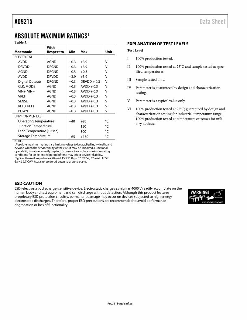
ABSOLUTE MAXIMUM RATINGS1 Table 5. Mnemonic
With Respect to
Min
Max
Unit
ELECTRICAL AVDD AGND −0.3 +3.9 V DRVDD DRGND −0.3 +3.9 V AGND DRGND −0.3 +0.3 V AVDD DRVDD −3.9 +3.9 V Digital Outputs DRGND −0.3 DRVDD + 0.3 V CLK, MODE AGND −0.3 AVDD + 0.3 V VIN+, VIN− AGND −0.3 AVDD + 0.3 V VREF AGND −0.3 AVDD + 0.3 V SENSE AGND −0.3 AVDD + 0.3 V REFB, REFT AGND −0.3 AVDD + 0.3 V PDWN AGND −0.3 AVDD + 0.3 V
ENVIRONMENTAL2 Operating Temperature Junction Temperature Lead Temperature (10 sec) Storage Temperature
−40 +85 °C 150 °C 300 °C −65 +150 °C
NOTES 1Absolute maximum ratings are limiting values to be applied individually, and beyond which the serviceability of the circuit may be impaired. Functional operability is not necessarily implied. Exposure to absolute maximum rating conditions for an extended period of time may affect device reliability. 2Typical thermal impedances 28-lead TSSOP: θJA = 67.7°C/W, 32-lead LFCSP: θJA = 32.7°C/W; heat sink soldered down to ground plane.
EXPLANATION OF TEST LEVELS Test Level
I 100% production tested.
II 100% production tested at 25°C and sample tested at spec-ified temperatures.
III Sample tested only.
IV Parameter is guaranteed by design and characterization testing.
V Parameter is a typical value only.
VI 100% production tested at 25°C; guaranteed by design and characterization testing for industrial temperature range; 100% production tested at temperature extremes for mili-tary devices.
ESD CAUTION ESD (electrostatic discharge) sensitive device. Electrostatic charges as high as 4000 V readily accumulate on the human body and test equipment and can discharge without detection. Although this product features proprietary ESD protection circuitry, permanent damage may occur on devices subjected to high energy electrostatic discharges. Therefore, proper ESD precautions are recommended to avoid performance degradation or loss of functionality.
Data Sheet AD9215
Rev. B | Page 7 of 36
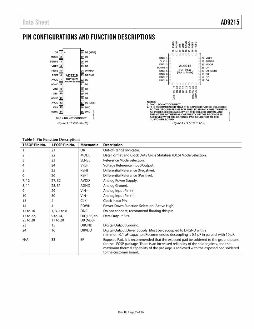
PIN CONFIGURATIONS AND FUNCTION DESCRIPTIONS
0287
4-A-
003
1
2
3
4
5
6
7
8
9
10
11
12
13
14
OR
MODE
SENSE
VREF
REFB
REFT
AVDD
AGND
VIN+
VIN–
AGND
AVDD
CLK
PDWN
D9 (MSB)
D8
D7
D6
DRVDD
DRGND
D5
D4
D3
D2
D1
D0 (LSB)
DNC
28
27
26
25
24
23
22
21
20
19
18
17
16
15
AD9215TOP VIEW
(Not to Scale)
DNC = DO NOT CONNECT
DNC
Figure 3. TSSOP (RU-28)
0287
4-A
-004
19
17
2021
18
14131211109 15 16
D5
D4
D3
D2
D1
(LSB
) D0
DR
GN
DD
RVD
D
32 31 30 29 28 27 26 25
AVD
DA
GN
DVI
N–
VIN
+A
GN
DA
VDD
REF
TR
EFB
222324
D8
D6
D9 (MSB)OR
D7
MODESENSEVREF1
2345678
DNCCLKDNC
PDWNDNCDNCDNCDNC
AD9215TOP VIEW
(Not to Scale)
NOTES1. DNC = DO NOT CONNECT.2. IT IS RECOMMENDED THAT THE EXPOSED PAD BE SOLDERED
TO THE GROUND PLANE FOR THE LFCSP PACKAGE. THERE ISAN INCREASED RELIABILITY OF THE SOLDER JOINTS, ANDTHE MAXIMUM THERMAL CAPABILITY OF THE PACKAGE ISACHIEVED WITH THE EXPOSED PAD SOLDERED TO THECUSTOMER BOARD.
Figure 4. LFCSP (CP-32-7)
Table 6. Pin Function Descriptions TSSOP Pin No. LFCSP Pin No. Mnemonic Description 1 21 OR Out-of-Range Indicator. 2 22 MODE Data Format and Clock Duty Cycle Stabilizer (DCS) Mode Selection. 3 23 SENSE Reference Mode Selection. 4 24 VREF Voltage Reference Input/Output. 5 25 REFB Differential Reference (Negative). 6 26 REFT Differential Reference (Positive). 7, 12 27, 32 AVDD Analog Power Supply. 8, 11 28, 31 AGND Analog Ground. 9 29 VIN+ Analog Input Pin (+). 10 30 VIN− Analog Input Pin (−). 13 2 CLK Clock Input Pin. 14 4 PDWN Power-Down Function Selection (Active High). 15 to 16 1, 3, 5 to 8 DNC Do not connect, recommend floating this pin. 17 to 22, 25 to 28
9 to 14, 17 to 20
D0 (LSB) to D9 (MSB)
Data Output Bits.
23 15 DRGND Digital Output Ground. 24 16 DRVDD Digital Output Driver Supply. Must be decoupled to DRGND with a
minimum 0.1 μF capacitor. Recommended decoupling is 0.1 μF in parallel with 10 μF. N/A 33 EP Exposed Pad. It is recommended that the exposed pad be soldered to the ground plane
for the LFCSP package. There is an increased reliability of the solder joints, and the maximum thermal capability of the package is achieved with the exposed pad soldered to the customer board.

AD9215 Data Sheet
Rev. B | Page 8 of 36
EQUIVALENT CIRCUITS
0287
4-A-
005
AVDD
MODE
Figure 5. Equivalent Analog Input Circuit
0287
4-A-
006
AVDD
MODE
20kΩ
Figure 6. Equivalent MODE Input Circuit
0287
4-A-
007
D9–D0,OR
DRVDD
Figure 7. Equivalent Digital Output Circuit
0287
4-A-
008
2.6kΩ
2.6kΩ
AVDD
CLK
Figure 8. Equivalent Digital Input Circuit
DEFINITIONS OF SPECIFICATIONS Aperture Delay
Aperture delay is a measure of the sample-and-hold amplifier (SHA) performance and is measured from the rising edge of the clock input to when the input signal is held for conversion.
Aperture Jitter
Aperture jitter is the variation in aperture delay for successive samples and can be manifested as frequency-dependent noise on the input to the ADC.
Clock Pulse Width and Duty Cycle
Pulse width high is the minimum amount of time that the clock pulse should be left in the Logic 1 state to achieve rated perfor-mance. Pulse width low is the minimum time the clock pulse should be left in the low state. At a given clock rate, these speci-fications define an acceptable clock duty cycle.
Differential Nonlinearity (DNL, No Missing Codes)
An ideal ADC exhibits code transitions that are exactly 1 LSB apart. DNL is the deviation from this ideal value. Guaranteed
no missing codes to 10-bit resolution indicate that all 1024 codes, respectively, must be present over all operating ranges.
Effective Number of Bits (ENOB)
For a sine wave, SINAD can be expressed in terms of the num-ber of bits. Using the following formula, it is possible to obtain a measure of performance expressed as N, the effective number of bits
N = (SINAD – 1.76)/6.02
Thus, the effective number of bits for a device for sine wave inputs at a given input frequency can be calculated directly from its measured SINAD.
Gain Error
The first code transition should occur at an analog value 1/2 LSB above negative full scale. The last transition should occur at an analog value 1 1/2 LSB below the positive full scale. Gain error is the deviation of the actual difference between the first and last code transitions and the ideal difference between the first and last code transitions.
Integral Nonlinearity (INL)
INL refers to the deviation of each individual code from a line drawn from “negative full scale” through “positive full scale.” The point used as negative full scale occurs 1/2 LSB before the first code transition. Positive full scale is defined as a level 1 1/2 LSB beyond the last code transition. The deviation is measured from the middle of each particular code to the true straight line.
Maximum Conversion Rate
The clock rate at which parametric testing is performed.
Minimum Conversion Rate
The clock rate at which the SNR of the lowest analog signal frequency drops by no more than 3 dB below the guaranteed limit.
Offset Error
The major carry transition should occur for an analog value 1/2 LSB below VIN+ = VIN−. Zero error is defined as the deviation of the actual transition from that point.
Out-of-Range Recovery Time
Out-of-range recovery time is the time it takes for the ADC to reacquire the analog input after a transient from 10% above positive full scale to 10% above negative full scale, or from 10% below negative full scale to 10% below positive full scale.
Output Propagation Delay
The delay between the clock logic threshold and the time when all bits are within valid logic levels.
Power Supply Rejection
The specification shows the maximum change in full scale from the value with the supply at the minimum limit to the value

Data Sheet AD9215
Rev. B | Page 9 of 36
with the supply at its maximum limit.
Signal-to-Noise and Distortion (SINAD) Ratio
SINAD is the ratio of the rms value of the measured input sig-nal to the rms sum of all other spectral components below the Nyquist frequency, including harmonics but excluding dc. The value for SINAD is expressed in decibels.
Signal-to-Noise Ratio (SNR)
SNR is the ratio of the rms value of the measured input signal to the rms sum of all other spectral components below the Nyquist frequency, excluding the first six harmonics and dc. The value for SNR is expressed in decibels.
Spurious-Free Dynamic Range (SFDR)
SFDR is the difference in dB between the rms amplitude of the input signal and the peak spurious signal.
Temperature Drift
The temperature drift for zero error and gain error specifies the maximum change from the initial (25°C) value to the value at TMIN or TMAX.
Total Harmonic Distortion (THD)
THD is the ratio of the rms sum of the first six harmonic com-ponents to the rms value of the measured input signal and is expressed as a percentage or in decibels.
Two-Tone SFDR
The ratio of the rms value of either input tone to the rms value of the peak spurious component. The peak spurious component may or may not be an IMD product. It may be reported in dBc (i.e., degrades as signal levels are lowered) or in dBFS (always related back to converter full scale).

AD9215 Data Sheet
Rev. B | Page 10 of 36
TYPICAL PERFORMANCE CHARACTERISTICS AVDD = 3.0 V, DRVDD = 2.5 V with DCS enabled, TA = 25°C, 2 V differential input, AIN = −0.5 dBFS, VREF = 1.0 V, unless otherwise noted.
0287
4-A
-062
–120
0
–20
–40
–60
–80
–100
0 52.5045.9439.3832.8126.2519.6913.136.56
AM
PLIT
UD
E (d
BFS
)
FREQUENCY (MHz)
AIN = –0.5dBFSSNR = 58.0ENOB = 9.4 BITSSFDR = 75.5dB
Figure 9. Single-Tone 32k FFT with fIN = 10.3 MHZ, fSAMPLE = 105 MSPS
0287
4-A
-063
–120
0
–20
–40
–60
–80
–100
0 52.5045.9439.3832.8126.2519.6913.136.56
AM
PLIT
UD
E (d
BFS
)
FREQUENCY (MHz)
AIN = –0.5dBFSSNR = 57.8ENOB = 9.4 BITSSFDR = 75.0dB
Figure 10. Single-Tone 32k FFT with fIN = 70.3 MHz, fSAMPLE = 105 MSPS
0287
4-A
-065
–120
0
–20
–40
–60
–80
–100
0 52.5045.9439.3832.8126.2519.6913.136.56
AM
PLIT
UD
E (d
BFS
)
FREQUENCY (MHz)
AIN = –0.5dBFSSNR = 57.7ENOB = 9.3 BITSSFDR = 75dB
Figure 11. Single-Tone 32k FFT with fIN = 100.3 MHz, fSAMPLE = 105 MSPS
0287
4-A
-012
ENCODE (MSPS)
dB
70
75
80
65
60
55
505 15 25 35 45 55 65 75 85
AIN = –0.5dBFS
1V p-p SFDR (dBc)
2V p-p SFDR (dBc)
1V p-p SNR (dB)
2V p-p SNR (dB)
Figure 12. AD9215-80 SNR/SFDR vs. fSAMPLE, fIN = 10.3 MHz
0287
4-A
-013
ENCODE (MSPS)
dB
70
75
80
65
60
55
505 15 25 35 45 55 65
AIN = –0.5dBFS2V p-p SFDR (dBc)
1V p-p SFDR (dBc)
1V p-p SNR (dB)
2V p-p SNR (dB)
Figure 13. AD9215-65 SNR/SFDR vs. fSAMPLE, fIN = 10.3 MHz
0287
4-A
-066
55
60
65
70
75
80
85
0 10080604020
dB
fSAMPLE (MSPS)
2V p-p SFDR
2V p-p SNR
Figure 14. AD9215-105 SNR/SFDR vs. fSAMPLE, fIN = 10.3 MHz
Data Sheet AD9215
Rev. B | Page 11 of 36
0287
4-A
-014
ANALOG INPUT LEVEL
dB 40
50
60
70
80
30
20
10
0–50 –40–45 –35 –25–30 –10–15–20 –5 0
2V p-p SNR (dB)
2V p-p SFDR (dBc)
1V p-p SFDR (dBc)
1V p-p SNR (dB)
80dB REFERENCE LINE
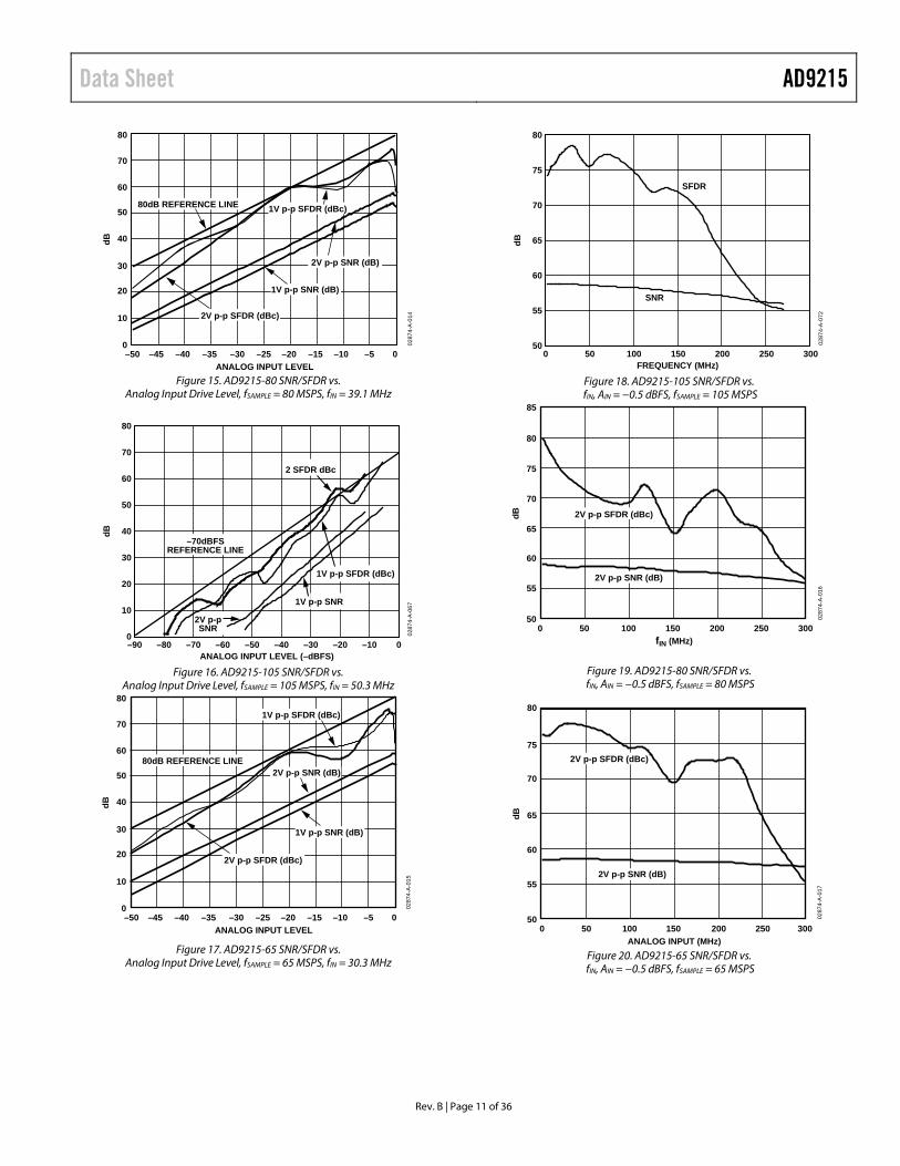
Figure 15. AD9215-80 SNR/SFDR vs.
Analog Input Drive Level, fSAMPLE = 80 MSPS, fIN = 39.1 MHz 02
874-
A-0
67
0
80
70
60
50
40
30
20
10
–90 –80 –70 –60 –50 –40 –30 –20 –10 0
dB
ANALOG INPUT LEVEL (–dBFS)
2V p-pSNR
1V p-p SNR
2 SFDR dBc
1V p-p SFDR (dBc)
–70dBFSREFERENCE LINE
Figure 16. AD9215-105 SNR/SFDR vs.
Analog Input Drive Level, fSAMPLE = 105 MSPS, fIN = 50.3 MHz
0287
4-A
-015
ANALOG INPUT LEVEL
dB 40
50
60
70
80
30
20
10
0–50 –40–45 –35 –25–30 –10–15–20 –5 0
2V p-p SNR (dB)
2V p-p SFDR (dBc)
1V p-p SFDR (dBc)
1V p-p SNR (dB)
80dB REFERENCE LINE
Figure 17. AD9215-65 SNR/SFDR vs.
Analog Input Drive Level, fSAMPLE = 65 MSPS, fIN = 30.3 MHz
0287
4-A
-072
50
55
60
65
70
75
80
0 50 100 150 200 250 300
SFDR
SNR
dB
FREQUENCY (MHz) Figure 18. AD9215-105 SNR/SFDR vs.
fIN, AIN = −0.5 dBFS, fSAMPLE = 105 MSPS
0287
4-A
-016
fIN (MHz)
dB
50
55
60
65
70
75
80
85
0 10050 150 250200 300
2V p-p SNR (dB)
2V p-p SFDR (dBc)
Figure 19. AD9215-80 SNR/SFDR vs. fIN, AIN = −0.5 dBFS, fSAMPLE = 80 MSPS
0287
4-A
-017
ANALOG INPUT (MHz)
dB
50
55
60
65
70
75
80
0 10050 150 250200 300
2V p-p SNR (dB)
2V p-p SFDR (dBc)
Figure 20. AD9215-65 SNR/SFDR vs.
fIN, AIN = −0.5 dBFS, fSAMPLE = 65 MSPS
AD9215 Data Sheet
Rev. B | Page 12 of 36
0287
4-A-
060
FREQUENCY (MHz)
dB
–120
–100
–80
–60
–40
–20
0
0 52.50039.37526.25013.125
AIN1, AIN2 = –7dBFSSFDR = 74dBc
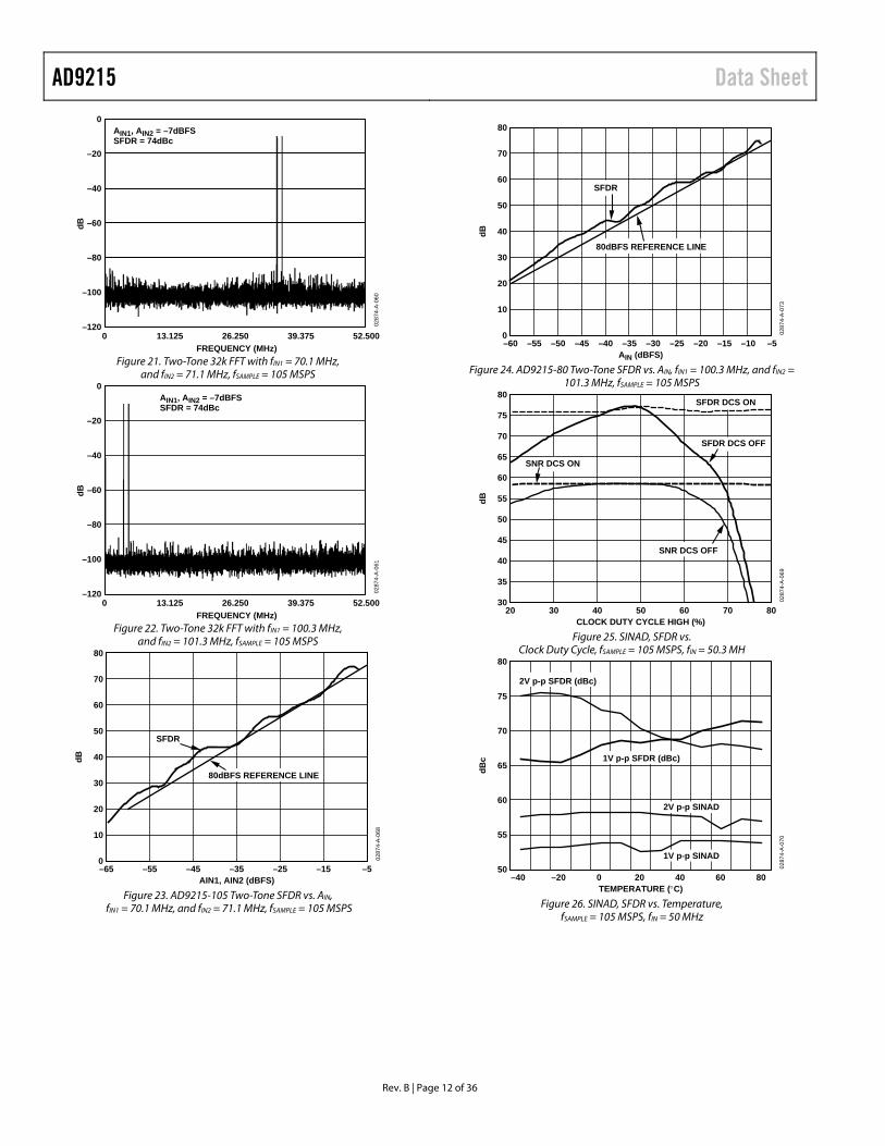
Figure 21. Two-Tone 32k FFT with fIN1 = 70.1 MHz, and fIN2 = 71.1 MHz, fSAMPLE = 105 MSPS
0287
4-A-
061
FREQUENCY (MHz)
dB
–120
–100
–80
–60
–40
–20
0
0 52.50039.37526.25013.125
AIN1, AIN2 = –7dBFSSFDR = 74dBc
Figure 22. Two-Tone 32k FFT with fIN1 = 100.3 MHz, and fIN2 = 101.3 MHz, fSAMPLE = 105 MSPS
0287
4-A-
068
0
80
70
60
50
40
30
20
10
–65 –55 –45 –35 –25 –15 –5
dB
AIN1, AIN2 (dBFS)
SFDR
80dBFS REFERENCE LINE
Figure 23. AD9215-105 Two-Tone SFDR vs. AIN, fIN1 = 70.1 MHz, and fIN2 = 71.1 MHz, fSAMPLE = 105 MSPS
0287
4-A-
073
0
80
70
60
50
40
30
20
10
–60 –5–10–15–20–25–30–35–40–45–50–55
dB
AIN (dBFS)
SFDR
80dBFS REFERENCE LINE
Figure 24. AD9215-80 Two-Tone SFDR vs. AIN, fIN1 = 100.3 MHz, and fIN2 = 101.3 MHz, fSAMPLE = 105 MSPS
0287
4-A-
069
30
80
75
70
65
60
55
50
45
40
35
20 30 40 50 60 70 80
dB
CLOCK DUTY CYCLE HIGH (%)
SFDR DCS ON
SFDR DCS OFF
SNR DCS ON
SNR DCS OFF
Figure 25. SINAD, SFDR vs. Clock Duty Cycle, fSAMPLE = 105 MSPS, fIN = 50.3 MH
0287
4-A-
070
50
55
60
65
70
75
80
–40 –20 0 20 40 60 80
dBc
TEMPERATURE (C)
2V p-p SFDR (dBc)
1V p-p SFDR (dBc)
2V p-p SINAD
1V p-p SINAD
Figure 26. SINAD, SFDR vs. Temperature, fSAMPLE = 105 MSPS, fIN = 50 MHz

Data Sheet AD9215
Rev. B | Page 13 of 36
0287
4-A
-025
TEMPERATURE (°C)
GA
IN E
RR
OR
(ppm
/°C)
10
20
30
0
40
–40
–30
–20
–10
–40 –20 0 20 6040 80
Figure 27. Gain vs. Temperature External 1 V Reference
0287
4-A
-064
–0.5
–0.4
–0.3
–0.2
–0.1
0
0.1
0.2
0.3
0.4
0.5
10248967686405123842561280
DN
L (L
SB)
CODE
Figure 28. AD9215-105 Typical DNL, fSAMPLE = 105 MSPS, fIN = 2.3 MHz
0287
4-A
-074
–0.6
–0.4
–0.2
0
0.2
0.4
0.6
10248967686405123842561280
INL
(LSB
)
CODE
Figure 29. AD9215-105 Typical INL, fSAMPLE = 105 MSPS, fIN = 2.3 MHz

AD9215 Data Sheet
Rev. B | Page 14 of 36
APPLYING THE AD9215 THEORY OF OPERATION The AD9215 architecture consists of a front-end SHA followed by a pipelined switched capacitor ADC. Each stage provides sufficient overlap to correct for flash errors in the preceding stages. The quantized outputs from each stage are combined into a final 10-bit result in the digital correction logic. The pipe-lined architecture permits the first stage to operate on a new input sample, while the remaining stages operate on preceding samples. Sampling occurs on the rising edge of the clock.
The input stage contains a differential SHA that can be config-ured as ac-coupled or dc-coupled in differential or single-ended modes. Each stage of the pipeline, excluding the last, consists of a low resolution flash ADC connected to a switched capacitor DAC and interstage residue amplifier (MDAC). The residue amplifier magnifies the difference between the reconstructed DAC output and the flash input for the next stage in the pipe-line. Redundancy is used in each one of the stages to facilitate digital correction of flash errors.
The output-staging block aligns the data, carries out the error correction, and passes the data to the output buffers. The output buffers are powered from a separate supply, allowing adjust-ment of the output voltage swing. During power-down, the output buffers go into a high impedance state.
Analog Input and Reference Overview
The analog input to the AD9215 is a differential switched capacitor SHA that has been designed for optimum perfor-mance while processing a differential input signal. The SHA input can support a wide common-mode range and maintain excellent performance, as shown in Figure 31. An input com-mon-mode voltage of midsupply minimizes signal-dependent errors and provides optimum performance.
0287
4-A
-028
H
H
VIN+
VIN–
CPAR
CPAR
T
T
0.5pF
0.5pF
T
T
Figure 30. Switched-Capacitor SHA Input
The clock signal alternatively switches the SHA between sample mode and hold mode (see Figure 30). When the SHA is switched into sample mode, the signal source must be capable of charging the sample capacitors and settling within one-half of a clock cycle. A small resistor in series with each input can help reduce the peak transient current required from the output stage of the driving source. Also, a small shunt capacitor can be
placed across the inputs to provide dynamic charging currents. This passive network creates a low-pass filter at the ADC’s in-put; therefore, the precise values are dependent upon the appli-cation. In IF undersampling applications, any shunt capacitors should be removed. In combination with the driving source impedance, they would limit the input bandwidth.
The analog inputs of the AD9215 are not internally dc biased. In ac-coupled applications, the user must provide this bias ex-ternally. VCM = AVDD/2 is recommended for optimum perfor-mance, but the device functions over a wider range with rea-sonable performance (see Figure 31).
0287
4-A
-071
40
45
50
55
60
65
70
75
80
85
0.25 0.75 1.25 1.75 2.25 2.75
dB
ANALOG INPUT COMMON-MODE VOLTAGE (V)
2V p-p SFDR
2V p-p SNR
Figure 31. AD9215-105 SNR, SFDR vs. Common-Mode Voltage
For best dynamic performance, the source impedances driving VIN+ and VIN− should be matched such that common-mode settling errors are symmetrical. These errors are reduced by the common-mode rejection of the ADC.
An internal differential reference buffer creates positive and negative reference voltages, REFT and REFB, respectively, that define the span of the ADC core. The output common mode of the reference buffer is set to midsupply, and the REFT and REFB voltages and span are defined as
REFT = 1/2 (AVDD + VREF)
REFB = 1/2 (AVDD − VREF)
Span = 2 × (REFT − REFB) = 2 × VREF
It can be seen from the equations above that the REFT and REFB voltages are symmetrical about the midsupply voltage and, by definition, the input span is twice the value of the VREF voltage.
The internal voltage reference can be pin-strapped to fixed val-ues of 0.5 V or 1.0 V or adjusted within the same range as dis-cussed in the Internal Reference Connection section. Maximum SNR performance is achieved with the AD9215 set to the largest input span of 2 V p-p. The relative SNR degradation is 3 dB

Data Sheet AD9215
Rev. B | Page 15 of 36
when changing from 2 V p-p mode to 1 V p-p mode.
The SHA may be driven from a source that keeps the signal peaks within the allowable range for the selected reference volt-age. The minimum and maximum common-mode input levels are defined as
VCMMIN = VREF/2
VCMMAX = (AVDD + VREF)/2
The minimum common-mode input level allows the AD9215 to accommodate ground-referenced inputs.
Although optimum performance is achieved with a differential input, a single-ended source may be driven into VIN+ or VIN−. In this configuration, one input accepts the signal, while the opposite input should be set to midscale by connecting it to an appropriate reference. For example, a 2 V p-p signal may be applied to VIN+ while a 1 V reference is applied to VIN−. The AD9215 then accepts a signal varying between 2 V and 0 V. In the single-ended configuration, distortion performance may degrade significantly as compared to the differential case. How-ever, the effect is less noticeable at lower input frequencies.
Differential Input Configurations
As previously detailed, optimum performance is achieved while driving the AD9215 in a differential input configuration. For baseband applications, the AD8138 differential driver provides excellent performance and a flexible interface to the ADC. The output common-mode voltage of the AD8138 is easily set to AVDD/2, and the driver can be configured in a Sallen Key filter topology to provide band limiting of the input signal.
0287
4-A-
030
AD8138 AD9215
VIN+
VIN–
AVDD
AGND1V p-p
R
R
C
C
499Ω
499Ω
499Ω
523Ω
49.9Ω
1kΩ
1kΩ0.1µF
VCM
Figure 32. Differential Input Configuration Using the AD8138
At input frequencies in the second Nyquist zone and above, the performance of most amplifiers is not adequate to achieve the true performance of the AD9215. This is especially true in IF undersampling applications where frequencies in the 70 MHz to 200 MHz range are being sampled. For these applications, differ-ential transformer coupling is the recommended input configura-tion. The value of the shunt capacitor is dependant on the input frequency and source impedance and should be reduced or re-moved. An example of this is shown in Figure 33.
0287
4-A-
031
AD9215
VIN+
VIN–
AVDD
AGND
2Vp-p
R
R
C
C49.9Ω
0.1µF
AVDD1kΩ
1kΩ
Figure 33. Differential Transformer-Coupled Configuration
The signal characteristics must be considered when selecting a transformer. Most RF transformers saturate at frequencies below a few MHz, and excessive signal power can also cause core saturation, which leads to distortion.
Single-Ended Input Configuration
A single-ended input may provide adequate performance in cost-sensitive applications. In this configuration, there is a deg-radation in SFDR and distortion performance due to the large input common-mode swing. However, if the source impedances on each input are kept matched, there should be little effect on SNR performance. Figure 34 details a typical single-ended input configuration.
0287
4-A-
032
2V p-p
R
R
C
C49.9Ω 0.1µF
10µF
10µF 0.1µF
AD9215
VIN+
VIN–
AVDD
AGND
AVDD1kΩ
1kΩ
1kΩ
1kΩ
Figure 34. Single-Ended Input Configuration
CLOCK INPUT AND CONSIDERATIONS Typical high speed ADCs use both clock edges to generate a variety of internal timing signals, and as a result may be sensi-tive to clock duty cycle. Commonly, a 5% tolerance is required on the clock duty cycle to maintain dynamic performance char-acteristics. The AD9215 contains a clock duty cycle stabilizer that retimes the nonsampling edge, providing an internal clock signal with a nominal 50% duty cycle. This allows a wide range of clock input duty cycles without affecting the performance of the AD9215. As shown in Figure 25, noise and distortion per-formance are nearly flat over a 50% range of duty cycle. For best ac performance, enabling the duty cycle stabilizer is recom-mended for all applications.
The duty cycle stabilizer uses a delay-locked loop (DLL) to cre-ate the nonsampling edge. As a result, any changes to the sam-pling frequency require approximately 100 clock cycles to allow the DLL to acquire and lock to the new rate.
AD9215 Data Sheet
Rev. B | Page 16 of 36
Table 7. Reference Configuration Summary Selected Mode
External SENSE Connection
Internal Op Amp Configuration
Resulting VREF (V)
Resulting Differential Span (V p-p)
Externally Supplied Reference AVDD N/A N/A 2 × External Reference Internal 0.5 V Reference VREF Voltage Follower (G = 1) 0.5 1.0 Programmed Variable Reference
External Divider Noninverting (1 < G < 2) 0.5 × (1 + R2/R1) 2 × VREF
Internally Programmed 1 V Reference
AGND to 0.2 V Internal Divider 1.0 2.0
Table 8. Digital Output Coding Code VIN+ − VIN− Input Span =
2 V p-p (V) VIN+ − VIN− Input Span = 1 V p-p (V)
Digital Output Offset Binary (D9••••••D0)
Digital Output Twos Complement (D9••••••D0)
1023 1.000 0.500 11 1111 1111 01 1111 1111 512 0 0 10 0000 0000 00 0000 0000 511 −0.00195 −0.000978 01 1111 1111 11 1111 1111 0 −1.00 −0.5000 00 0000 0000 10 0000 0000
High speed, high resolution ADCs are sensitive to the quality of the clock input. The degradation in SNR at a given full-scale input frequency (fINPUT) due only to aperture jitter (tA) can be calculated with the following equation
SNR Degradation = 20 × log10 [2 × π × fINPUT × tA]
In the equation, the rms aperture jitter, tA, represents the root-sum square of all jitter sources, which include the clock input, analog input signal, and ADC aperture jitter specification. Undersampling applications are particularly sensitive to jitter.
The clock input should be treated as an analog signal in cases where aperture jitter may affect the dynamic range of the AD9215. Power supplies for clock drivers should be separated from the ADC output driver supplies to avoid modulating the clock signal with digital noise. Low jitter, crystal-controlled oscillators make the best clock sources. If the clock is generated from another type of source (by gating, dividing, or other methods), it should be retimed by the original clock at the last step.
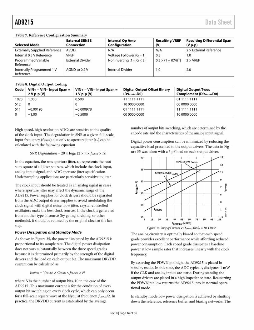
Power Dissipation and Standby Mode
As shown in Figure 35, the power dissipated by the AD9215 is proportional to its sample rate. The digital power dissipation does not vary substantially between the three speed grades because it is determined primarily by the strength of the digital drivers and the load on each output bit. The maximum DRVDD current can be calculated as
IDRVDD = VDRVDD × CLOAD × fCLOCK × N
where N is the number of output bits, 10 in the case of the AD9215. This maximum current is for the condition of every output bit switching on every clock cycle, which can only occur for a full-scale square wave at the Nyquist frequency, fCLOCK/2. In practice, the DRVDD current is established by the average
number of output bits switching, which are determined by the encode rate and the characteristics of the analog input signal.
Digital power consumption can be minimized by reducing the capacitive load presented to the output drivers. The data in Fig-ure 35 was taken with a 5 pF load on each output driver.
0287
4-A
-075
15
35
30
25
20
40
1055 15 25 35 45 55 65 75 85 95
I AVD
D (m
A)
I DR
VDD
–1
1
3
5
7
9
11
13
15
fSAMPLE (MSPS)
AD9215-105 IAVDD
AD9215-65/80 IAVDD
IDRVDD
Figure 35. Supply Current vs. fSAMPLE for fIN = 10.3 MHz
The analog circuitry is optimally biased so that each speed grade provides excellent performance while affording reduced power consumption. Each speed grade dissipates a baseline power at low sample rates that increases linearly with the clock frequency.
By asserting the PDWN pin high, the AD9215 is placed in standby mode. In this state, the ADC typically dissipates 1 mW if the CLK and analog inputs are static. During standby, the output drivers are placed in a high impedance state. Reasserting the PDWN pin low returns the AD9215 into its normal opera-tional mode.
In standby mode, low power dissipation is achieved by shutting down the reference, reference buffer, and biasing networks. The
Data Sheet AD9215
Rev. B | Page 17 of 36
decoupling capacitors on REFT and REFB are discharged when entering standby mode and then must be recharged when returning to normal operation. As a result, the wake-up time is related to the time spent in standby mode, and shorter standby cycles result in proportionally shorter wake-up times. With the recommended 0.1 μF and 10 μF decoupling capacitors on REFT and REFB, it takes approximately one second to fully discharge the reference buffer decoupling capacitors and 7 ms to restore full operation.
Digital Outputs
The AD9215 output drivers can be configured to interface with 2.5 V or 3.3 V logic families by matching DRVDD to the digital supply of the interfaced logic. The output drivers are sized to provide sufficient output current to drive a wide variety of logic families. However, large drive currents tend to cause current glitches on the supplies that may affect converter performance. Applications requiring the ADC to drive large capacitive loads or large fanouts may require external buffers or latches.
Timing
The AD9215 provides latched data outputs with a pipeline delay of five clock cycles. Data outputs are available one propagation delay (tOD) after the rising edge of the clock signal. Refer to Fig-ure 2 for a detailed timing diagram.
The length of the output data lines and loads placed on them should be minimized to reduce transients within the AD9215; these transients can detract from the converter’s dynamic per-formance.
The lowest typical conversion rate of the AD9215 is 5 MSPS. At clock rates below 5 MSPS, dynamic performance may degrade.
Voltage Reference
A stable and accurate 0.5 V voltage reference is built into the AD9215. The input range can be adjusted by varying the refer-ence voltage applied to the AD9215, using either the internal reference or an externally applied reference voltage. The input span of the ADC tracks reference voltage changes linearly. Max-imum SNR and DNL performance is achieved with the AD9215 set to the largest input span of 2 V p-p.
Internal Reference Connection
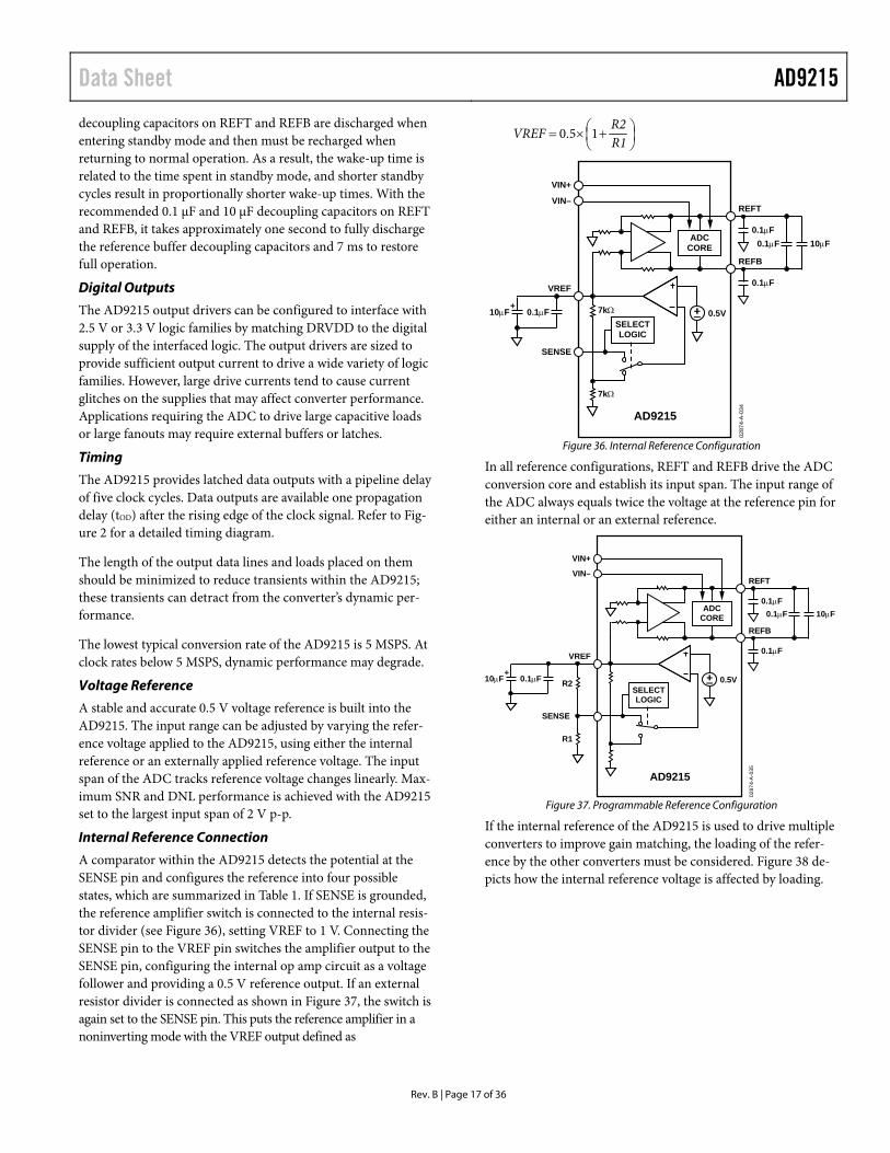
A comparator within the AD9215 detects the potential at the SENSE pin and configures the reference into four possible states, which are summarized in Table 1. If SENSE is grounded, the reference amplifier switch is connected to the internal resis-tor divider (see Figure 36), setting VREF to 1 V. Connecting the SENSE pin to the VREF pin switches the amplifier output to the SENSE pin, configuring the internal op amp circuit as a voltage follower and providing a 0.5 V reference output. If an external resistor divider is connected as shown in Figure 37, the switch is again set to the SENSE pin. This puts the reference amplifier in a noninverting mode with the VREF output defined as
R1R2
VREF 15.0
0287
4-A-
034
10F+
0.1F
VREF
SENSE
0.5V
7k
7k
AD9215
VIN–
VIN+
REFT
0.1F0.1F 10F
0.1F
REFB
SELECTLOGIC
ADCCORE
Figure 36. Internal Reference Configuration
In all reference configurations, REFT and REFB drive the ADC conversion core and establish its input span. The input range of the ADC always equals twice the voltage at the reference pin for either an internal or an external reference.
0287
4-A
-035
10F+
0.1F
VREF
R2
R1
SENSE
0.5V
AD9215
VIN–
VIN+
REFT
0.1F0.1F 10F
0.1F
REFB
SELECTLOGIC
ADCCORE
Figure 37. Programmable Reference Configuration
If the internal reference of the AD9215 is used to drive multiple converters to improve gain matching, the loading of the refer-ence by the other converters must be considered. Figure 38 de-picts how the internal reference voltage is affected by loading.

AD9215 Data Sheet
Rev. B | Page 18 of 36
0287
4-A
-036
ILOAD (mA)
VREF
ER
RO
R (%
)
0
0.05
–0.25
–0.20
–0.15
–0.10
–0.05
0 0.5 1.0 1.5 2.0 2.5 3.0
VREF = 0.5V
VREF = 1.0V
Figure 38. VREF Accuracy vs. Load
External Reference Operation
The use of an external reference may be necessary to enhance the gain accuracy of the ADC or improve thermal drift charac-teristics. When multiple ADCs track one another, a single refer-ence (internal or external) may be necessary to reduce gain matching errors to an acceptable level. A high precision external reference may also be selected to provide lower gain and offset temperature drift. Figure 39 shows the typical drift characteris-tics of the internal reference in both 1 V and 0.5 V modes.
0287
4-A
-037
TEMPERATURE (°C)
VREF
ER
RO
R (%
) 0.4
0.5
0.6
0.3
0.2
0.1
0–40 –20 0 20 40 60 80
VREF = 1.0V
VREF = 0.5V
Figure 39. Typical VREF Drift
When the SENSE pin is tied to AVDD, the internal reference is disabled, allowing the use of an external reference. An internal reference buffer loads the external reference with an equivalent 7 kΩ load. The internal buffer still generates the positive and negative full-scale references, REFT and REFB, for the ADC core. The input span is always twice the value of the reference voltage; therefore, the external reference must be limited to a maximum of 1 V.
Operational Mode Selection
As discussed earlier, the AD9215 can output data in either offset binary or twos complement format. There is also a provision for enabling or disabling the clock duty cycle stabilizer (DCS). The MODE pin is a multilevel input that controls the data format and DCS state. For best ac performance, enabling the duty cycle stabilizer is recommended for all applications. The input threshold values and corresponding mode selections are out-lined in Table 9.
As detailed in Table 9, the data format can be selected for either offset binary or twos complement.
Table 9. Mode Selection MODE Voltage Data Format Duty Cycle Stabilizer AVDD Twos Complement Disabled 2/3 AVDD Twos Complement Enabled 1/3 AVDD Offset Binary Enabled AGND (Default) Offset Binary Disabled
The MODE pin is internally pulled down to AGND by a 20 kΩ resistor.
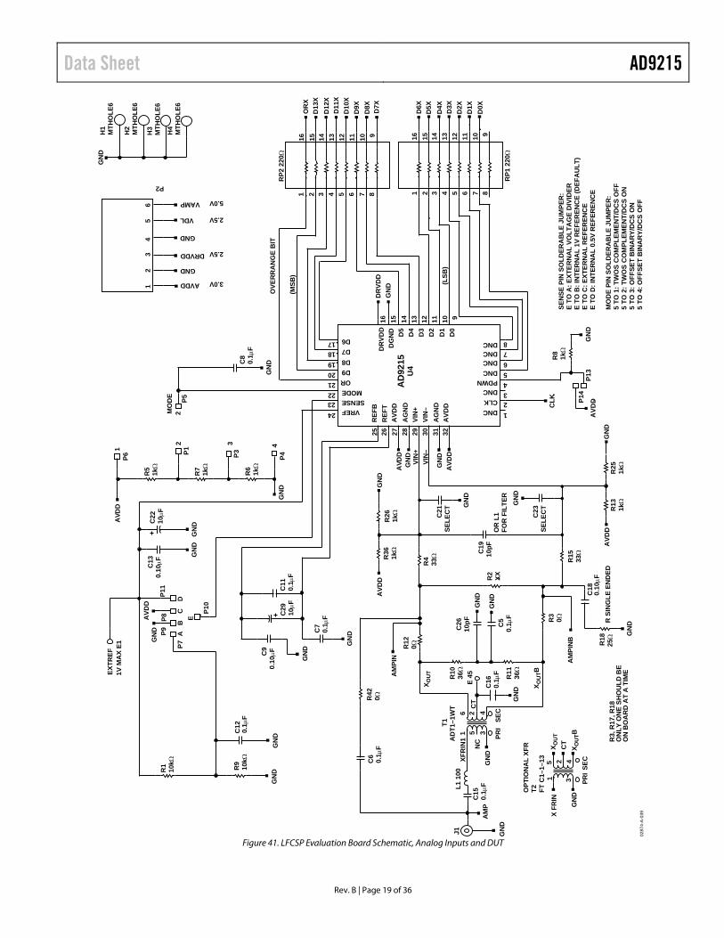
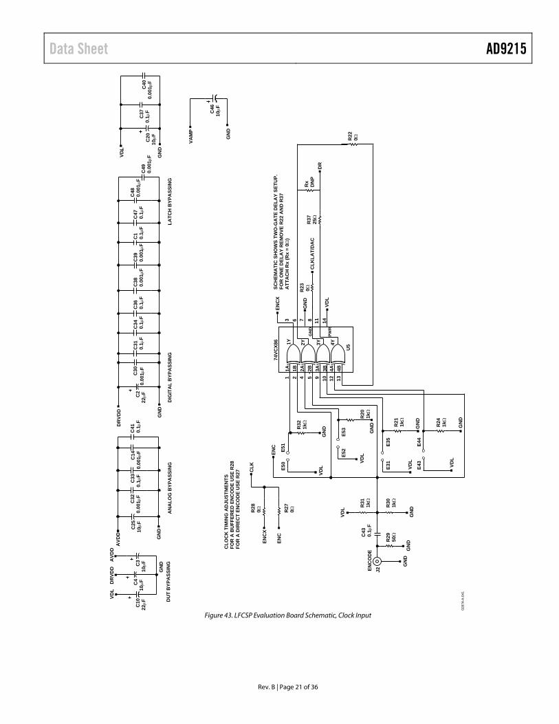
EVALUATION BOARD The AD9215 evaluation board is no longer in production. The following evaluation board documentation is provided for in-formational purposes only.
The AD9215 evaluation board provides all of the support cir-cuitry required to operate the ADC in its various modes and configurations. The converter can be driven differentially through an AD8351 driver, a transformer, or single-ended. Sep-arate power pins are provided to isolate the DUT from the sup-port circuitry. Each input configuration can be selected by proper connection of various jumpers (refer to the schematics). Figure 40 shows the typical bench characterization setup used to evaluate the ac performance of the AD9215. It is critical that signal sources with very low phase noise (<1 ps rms jitter) be used to realize the ultimate performance of the converter. Prop-er filtering of the input signal, to remove harmonics and lower the integrated noise at the input, is also necessary to achieve the specified noise performance.
Complete schematics and layout plots follow that demonstrate the proper routing and grounding techniques that should be applied at the system level.
0287
4-A-
038
R AND S SMG, 2V p-pSIGNAL SYNTHESIZER
R AND S SMG, 2V p-pSIGNAL SYNTHESIZER
REFIN
10MHzREFOUT
BAND-PASSFILTER
3.0V– + – + – +– +
2.5V 5.0V
AVDD DRVDDGND GND VDL VAMP
XFMRINPUT
CLK
P12AD9215EVALUATION BOARD
DATACAPTURE
ANDPROCESSING
2.5V
Figure 40. Evaluation Board Connections
Data Sheet AD9215
Rev. B | Page 19 of 36
0287
4-A
-039
29
12
34
56
P13
P14
XFR
IN1
OPT
ION
AL
XFR
T2 FT C
1–1–
13
NC
CT
1
T1A
DT1
–1W
T6 2
34
5
12
345
R S
ING
LE E
ND
EDR
1825
ΩR
3, R
17, R
18O
NLY
ON
E SH
OU
LD B
EO
N B
OA
RD
AT
A T
IMEEX
TREF
1V M
AX
E1
R1
10kΩ
R9
10kΩ
0.1µ
FC
12
C9
0.10
µFG
ND
GN
DG
ND
GN
D
GN
DA
VDD
C29
10µF
C11
0.1µ
F
C7
0.1µ
F
GN
D
GN
D
AVD
D
P7A
BC
D
P9P8
P11
P10
E
C13
0.10
µFC
2210
µF
P6
P1 P3 P4
1
2 3 4
GN
D
GN
DC8
0.1µ
F
P52M
OD
E
25 26 27 28 30 31 32
2423222120191817
12345678
REF
BR
EFT
AG
ND
VIN
+
AG
ND
AVD
D
AVD
D
VIN
–
AD
9215
U4
VREFSENSEMODE
D9OR
D8D7D6
DR
VDD
DG
ND D5
D3
D4
D2
D1
D0
16 15 14 13 12 11 10 9
DNCCLKDNC
DNCDNCDNCDNC
PDWN
(LSB
)
DR
VDD
GN
D
1 2 3 4 5 6 7 81 2 3 4 5 6 7 8
16 15 14 13 12 11 10 916 15 14 13 12 11 10 9
OR
XD
13X
D12
X
D10
XD
11X
D9X
D8X D7X
D6X
D5X
D4X
D2XD3X
D1X
D0X
(MSB
)
OVE
RR
AN
GE
BIT
AVDD
GND
DRVDD
VDL
GND
VAMP
P2
GN
DH
1M
THO
LE6
H2
MTH
OLE
6
H3
MTH
OLE
6
H4
MTH
OLE
6
3.0V
2.5V
2.5V
5.0V
RP2
220
Ω
RP1
220
Ω
SEN
SE P
IN S
OLD
ERA
BLE
JU
MPE
R:
E TO
A: E
XTER
NA
L VO
LTA
GE
DIV
IDER
E TO
B: I
NTE
RN
AL
1V R
EFER
ENC
E (D
EFA
ULT
)E
TO C
: EXT
ERN
AL
REF
EREN
CE
E TO
D: I
NTE
RN
AL
0.5V
REF
EREN
CE
MO
DE
PIN
SO
LDER
AB
LE J
UM
PER
:5
TO 1
: TW
OS
CO
MPL
EMEN
T/D
CS
OFF
5 TO
2: T
WO
S C
OM
PLEM
ENT/
DC
S O
N5
TO 3
: OFF
SET
BIN
AR
Y/D
CS
ON
5 TO
4: O
FFSE
T B
INA
RY/
DC
S O
FF
GN
D
R8
1kΩ
CLK
AVD
D
GN
DR
251k
ΩR
131k
Ω
R15
33Ω
AVD
D
GN
D
GN
D
GN
DC
1910
pFO
R L
1FO
R F
ILTE
R
GN
DAVD
D
R4
33ΩR36
1kΩ
R26
1kΩ
GN
D
AVD
D
AVD
D
GN
D
GN
D
VIN
+VI
N–
C21
SELE
CT
C23
SELE
CT
R2
XX
R10
36Ω
R12
0Ω
AM
PIN
X OU
T
GN
D X OU
TB
R3
0Ω
R11
36Ω
C5
0.1µ
F
C26
10pF
E 45
C16
0.1µ
F
R42
0ΩC
6 0.1µ
F
GN
D
GN
D
AM
P
AM
PIN
B
C15
0.1µ
FL1 1
00
GN
DPR
ISE
C
PRI
SEC
GN
D
C18
0.10
µF
X FR
IN
X OU
TBC
TX O
UT
J1
R5
1kΩ
R7
1kΩ
R6
1kΩ
Figure 41. LFCSP Evaluation Board Schematic, Analog Inputs and DUT

AD9215 Data Sheet
Rev. B | Page 20 of 36
0287
4-A
-040
DR
XD
13X
GN
D
D2X D1X
GN
DD
0X
D11
XD
12X
DR
VDD
D10
XD
9XG
ND
D8X
D7X
D5XD6X
GN
DD
4XD
3XD
RVD
D
2CLK
2DB
2D7
GN
D2D
62D
5
1D2
1D1
1CLK
1
2D4
V CC
2D3
GN
D2D
22D
1
1D7
1D6
1D5
1D8
GN
D
1D4
1D3
GN
D
2OE
2QB
2Q7
2Q6
2Q5
1Q2
1Q1
1OE
2Q4
2Q3
GN
D
GN
D
2Q2
2Q1
1Q8
1Q7
1Q5
GN
D
V CC
V CC
V CC
1Q6
1Q4
1Q3
GN
D
25 26 27 28 29 30 31 32 33 34 35 36 37 38 39 40 41 42 43 44 45 46 47 48
24 23 22 21 20 19 18 17 16 15 14 13 12 11 10 9 8 7 6 5 4 3 2 1IN
OU
T
CLK
AT/
DA
C
U1
74LV
TH16
2374
CLK
LAT/
DA
C
GN
D
GN
D
DR
VDD
GN
D
GN
D
DR
VDD
GN
D
GN
D
DR
YM
SB LSB
2 4 6 8 10 12 14 16 18 20 22 24 26 28 30 32 34 36 38 40
2 4 6 8 10 12 14 16 18 20 22 24 26 28 30 32 34 36 38 40
1 3 5 7 9 11 13 15 17 19 21 23 25 27 29 31 33 35 37 39
1 3 5 7 9 11 13 15 17 19 21 23 25 27 29 31 33 35 37 39
GN
DD
RG
ND
MSB
DR
Y GN
D
AM
PIN
AM
PIN
B
GN
D
VAM
P
GN
D
GN
D
GN
D
GN
DVA
MP
GN
D GN
D
VAM
P
GN
D
P12
HEA
DER
40
C27
0.1µ
F
C45
0.1µ
F
C28
0.1µ
F
C35
0.10
µF
C24
10µF
C17
0.1µ
F
R16
0Ω
R14
25Ω
R40
10kΩ
PWD
N 1
RG
P1 2
INH
I 3
INLO
4
RPG
2 5
R41
10kΩ
R35
25Ω
R33
25Ω
R34
1.2k
Ω
R19
50Ω
AM
P IN
AM
P
R17
0Ω
R38
1kΩ
R39
1kΩ
U3
AD
8351
POW
ER D
OW
NU
SE R
40 O
R R
41C
440.
1µF
GN
D6
CO
MM
7 O
PLO
8 O
PHI
9 VP
OS
10 V
OC
M
Figure 42. LFCSP Evaluation Board, Digital Path
Data Sheet AD9215
Rev. B | Page 21 of 36
0287
4-A
-041
C10
22µF
C4
10µF
C3
10µF
C25
10µF
C32
0.00
1µF
C33
0.1µ
FC
140.
001µ
F
VDL
DR
VDD
AVD
D
GN
DG
ND
AVD
D
DU
T B
YPA
SSIN
G
CLO
CK
TIM
ING
AD
JUST
MEN
TSFO
R A
BU
FFER
ED E
NC
OD
E U
SE R
28FO
R A
DIR
ECT
ENC
OD
E U
SE R
27
AN
ALO
G B
YPA
SSIN
GD
IGIT
AL
BYP
ASS
ING
GN
D
DR
VDD
C41
0.1µ
FC
222
µFC
300.
001µ
FC
310.
1µF
C46
10µF
C34
0.1µ
FC
360.
1µF
C38
0.00
1µF
C1
0.1µ
FC
470.
1µF
C48
0.00
1µF
C49
0.00
1µF
C20
10µF
C37
0.1µ
FC
400.
001µ
F
GN
D
GN
D
VAM
P
VDL
C39
0.00
1µF
ENC
X
CLK
ENC
ENC
OD
E
R27
0ΩR
321k
ΩR
23 0ΩR
3725
Ω
R22
0Ω
Rx
DN
P
R28
0Ω
E50
E51
ENC
VDL VD
LVDLE5
2E5
3
E31
E35
E43
E44G
ND
GN
D
GN
D
PWR
GN
DC
LKLA
T/D
AC
VDL
GN
D
VDL
GN
D
C43
0.1µ
FR
311k
ΩR
201k
Ω
R21
1kΩ
R24
1kΩ
R30
1kΩ
R29
50Ω
GN
D
J2
GN
D
VDL
GN
D
11Y
U52Y 3Y 4Y
2 4 5 9 10
3 6 7 8 11 1412 13
74VC
X86
ENC
X
1B1A 2B2A 3B3A 4B4A
DR
SCH
EMA
TIC
SH
OW
S TW
O-G
ATE
DEL
AY
SETU
P.FO
R O
NE
DEL
AY
REM
OVE
R22
AN
D R
37A
TTA
CH
Rx
(Rx
= 0Ω
)
LATC
H B
YPA
SSIN
G
Figure 43. LFCSP Evaluation Board Schematic, Clock Input

AD9215 Data Sheet
Rev. B | Page 22 of 36
0287
4-A
-042
Figure 44. LFCSP Evaluation Board Layout, Primary Side
0287
4-A
-043
Figure 45. LFCSP Evaluation Board Layout, Secondary Side

Data Sheet AD9215
Rev. B | Page 23 of 36
0287
4-A
-044
Figure 46. LFCSP Evaluation Board Layout, Ground Plane
0287
4-A
-045
Figure 47. LFCSP Evaluation Board Layout, Power Plane

AD9215 Data Sheet
Rev. B | Page 24 of 36
0287
4-A
-046
Figure 48. LFCSP Evaluation Board Layout, Primary Silkscreen
0287
4-A
-047
Figure 49. LFCSP Evaluation Board Layout, Secondary Silkscreen
Data Sheet AD9215
Rev. B | Page 25 of 36
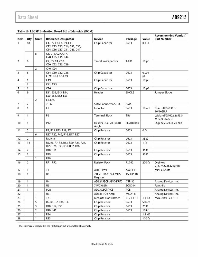
Table 10. LFCSP Evaluation Board Bill of Materials (BOM) Item
Qty
Omit1
Reference Designator
Device
Package
Value
Recommended Vendor/ Part Number
1 18 C1, C5, C7, C8, C9, C11, C12, C13, C15, C16, C31, C33, C34, C36, C37, C41, C43, C47
Chip Capacitor 0603 0.1 μF
8 C6, C18, C27, C17, C28, C35, C45, C44
2 8 C2, C3, C4, C10, C20, C22, C25, C29
Tantalum Capacitor TAJD 10 μF
2 C46, C24, 3 8 C14, C30, C32, C38,
C39 C40, C48, C49 Chip Capacitor 0603 0.001
μF
4 1 C19 Chip Capacitor 0603 10 pF 2 C21, C23
5 1 C26 Chip Capacitor 0603 10 pF 6 9 E31, E35, E43, E44,
E50, E51, E52, E53 Header EHOLE Jumper Blocks
2 E1, E45 7 2 J1, J2 SMA Connector/50 Ω SMA 8 1 L1 Inductor 0603 10 nH Coilcraft/0603CS-
10NXGBU 9 1 P2 Terminal Block TB6 Wieland/25.602.2653.0
z5-530-0625-0 10 1 P12 Header Dual 20-Pin RT
Angle HEADER40 Digi-Key S2131-20-ND
11 5 R3, R12, R23, R18, RX Chip Resistor 0603 0 Ω 6 R37, R22, R42, R16, R17, R27
12 2 R4, R15 Chip Resistor 0603 33 Ω 13 14 R5, R6, R7, R8, R13, R20, R21, R24,
R25, R26, R30, R31, R32, R36 Chip Resistor 0603 1 Ω
14 2 R10, R11 Chip Resistor 0603 36 Ω 15 1 R29 Chip Resistor 0603 50 Ω
1 R19 16 2 RP1, RR2 Resistor Pack R_742 220 Ω Digi-Key
CTS/742C163220JTR 17 1 T1 ADT1-1WT AWT1-T1 Mini-Circuits 18 1 U1 74LVTH162374 CMOS
Register TSSOP-48
19 1 U4 AD9215BCP ADC (DUT) CSP-32 Analog Devices, Inc. 20 1 U5 74VCX86M SOIC-14 Fairchild 21 1 PCB AD9XXBCP/PCB PCB Analog Devices, Inc. 22 1 U3 AD8351 Op Amp MSOP-8 Analog Devices, Inc. 23 1 T2 MACOM Transformer ETC1-1-13 1-1 TX MACOM/ETC1-1-13 24 5 R9, R1, R2, R38, R39 Chip Resistor 0603 Select 25 3 R18, R14, R35 Chip Resistor 0603 25 Ω 26 2 R40, R41 Chip Resistor 0603 10 kΩ 27 1 R34 Chip Resistor 1.2 kΩ 28 1 R33 Chip Resistor 110 Ω 1 These items are included in the PCB design but are omitted at assembly.

AD9215 Data Sheet
Rev. B | Page 26 of 36
02874-A-048
OR
X
D5X
D6X
D7X
D8X
D9X
+ +
AG
ND
VIN
+
AVD
D
CLK
MO
DE
OR
PWD
N
REF
BR
EFT
SEN
SEVR
EF
VIN
–A
GN
DA
VDD
D0
D1
D2
D3
D4
D5
D6
D7
D8
D9
DR
GN
DD
RVD
D
DN
CD
NC
PRI
SEC
CD
BA
MO
DE
SELE
CT
F GE H
MO
DE
SELE
CT
CO
NFI
GU
RA
TIO
NE:
2C/D
CS
OFF
F:2C
/DC
S O
NG
:OB
/DC
S O
NH
:OB
/DC
S O
FF
(LSB
)
(MSB
)
OPT
ION
AL
OPT
ION
AL
DIF
FER
ENTI
AL
INPU
T
AN
ALO
G IN
PUT
OPT
ION
S1.
R6,
R34
FO
R D
IFFE
REN
TIA
L O
PER
ATI
ON
2. C
1, C
33 F
OR
OP
AM
P O
PER
ATI
ON
3. R
7, R
46, R
5, C
9, C
23 F
OR
SIN
GLE
-EN
DED
OPE
RA
TIO
N
CO
MM
ON
MO
DE
PLEA
SE J
UM
PER
E45
TO
E32
DC
VO
LTA
GE
AD
JUST
OR
JU
MPE
R E
45 T
O E
12 C
APA
CIT
OR
TO
GR
OU
ND
OVE
RR
AN
GE
BIT
E9E1
1
GN
D
GN
D
AVD
D
AIN
AIN
AM
P
J1L1 10nH
GN
D
AVD
D
E19
E16 E17SE
NSE
GN
D
VREF
OR
1
8 97 1321 145 63 4 10 11 1217181920212225262728 2324 16 15
DEV
ICE
= A
D92
15U
1PA
RTS
= 1
C29
10F
AM
PIN
AM
PIN
GN
D
GN
D
GN
D
GN
DA
VDD
GN
DA
VDD
1 5 3426
T1
GN
D
GN
D
910121314152 3 4 5 6 7 81
16 11
CLK
GN
DG
ND
E7 E8E2E5
E21 E20
E18
E22
E23
AVD
D
E1 E3 E4E6
2 3 4 5 6 7 81
9101213141516 11
E45
E12
CO
M
GN
D
3.0V
5.0V
2.5V
3.0V
3.0VVDL
13
24
P2
13
24
VAMP
GND
VCLK
GND
GND
DRVDD
AVDD
AVD
DG
ND
GN
D
DR
VDD
GN
D
NC
X
D4X
D3X
D2X
D1X
D0X
NC
2X
GN
DA
VDD
GN
D
GN
D
GN
D
DR
VDD
VDL
E29E28
E27
E26 E25
E24
VCLK
AVD
D
GN
DG
ND
REF
EREN
CE
CO
NFI
GU
RA
TIO
NA
: EXT
ERN
AL
VOLT
AG
E D
IVID
ER R
EFER
ENC
EB
: IN
TER
NA
L 1V
REF
EREN
CE
C: E
XTER
NA
L R
EFER
ENC
ED
: IN
TER
NA
L 0.
5V R
EFER
ENC
E 1V
MA
X
SIN
GLE
-EN
DED
INPU
T O
PER
ATI
ON
1. P
LAC
E R
7( 5
0),
R5(
0
) AN
D R
46 (2
5)
2. P
LAC
E C
23 (0
.1F
), C
9 (0
.1F
)3.
REM
OVE
C33
, C1,
R34
, R6,
C32
RP2
220
RP1
220
R11
1k
R29
1k
R24
1k
R21
33
R19
33R
441k
R
451k
R34 0R6
0
R25
25
R32
36
R33
36
R5
0
R16
XX
R8
1k
R10
1k
R9
1k
R4
10k
R15
10k
R7
50
C32
0.1
FC
70.
001
F
C9
0.1
F
C6
0.1
FC16
0.1
F
C13
0.1
F
C15
0.1
F
OPT
ION
AL
E32
GN
D
AVD
D
GN
DG
NDR3
5k
R1
10
C14
0.1
FC
120.
1F
C23
0.1
F
C11
0.1
F
C5
10pF
C8
10pF
C18
0.1
F
C30
0.1
FC
5210
F
C17
0.1
F
Figure 50. TSSOPP Evaluation Board Schematic, Analog Inputs and DUT
Data Sheet AD9215
Rev. B | Page 27 of 36
CPY7Y6Y5Y4Y3Y2Y1Y0
VCC
GN
DX7X6X5X4X3X2X1X0O
E
CPY7Y6Y5Y4Y3Y2Y1Y0
VCC
GN
DX7X6X5X4X3X2X1X0O
E
P2P4P6P8P10
P12
P14
P16
P18
P20
P22
P24
P26
P28
P1P3P5P7P9P11
P13
P15
P17
P19
P21
P23
P25
P27
P30
P29
P32
P31
P34
P33
P35
P38
P37
P40
P39
P36
MSB
MSB LS
B
OU
T O
F R
AN
GE
BIT
STR
AP
THIS
AT
ASS
EMB
LY
U2
11121314151617181920
10987654321
U3
74LV
T574
DEV
ICE
= 74
LVT5
74A
910121314152 3 4 5 6 7 81
16 11
RP4
220Ω
CLK
LAT/
DA
C
CLK
LAT/
DA
C
GN
D
GN
DG
ND
GN
D91012131415
2 3 4 5 6 7 8116 11
RP3
220Ω
NC
X
GN
DD
4X D3X
D2X
D1X
D0X
VDL
GN
D
VDL
1110
202 3 4 5 6 7 8 9
19 18 17 16 15 14 13 12
1
U4
74LV
T574
DEV
ICE
= 74
LVT5
74A
VDL
E30 E1
4
GN
D
DR
XG
ND
GN
D
GN
D
GN
D
D5X
D6X
D7X
D8X
D9X
OR
X
GN
D GN
D
NC
2X
GN
D
GN
D
GN
D
E13
GN
D
RG
P2IN
LOIN
HI
RG
P1PW
UP
VAM
P 54321
VAM
PG
ND
CO
MM
OPL
OO
PHI
VPO
SVO
CM
+
GN
D
GN
D
678910
U6
DEV
ICE
= A
D83
51
VAM
P
GN
D
GN
D
AM
P
R31
100Ω
R51
25Ω
R50
25Ω
R49
1kΩ
R48
1kΩ
R27 0ΩR17 0Ω
R30
1.2k
ΩR
3625
Ω
R20
150Ω
R22
10kΩ
R47
10kΩ
R28 0Ω
R23
100Ω
C45
0.1µ
F
C44
0.1µ
F
C31
10pF
C41
0.1µ
FC
420.
1µF
C33
0.1µ
F
C1
0.1µ
F
C43
0.00
1µF
AM
PIN
AM
PIN
C47
10µF
02874-A-049
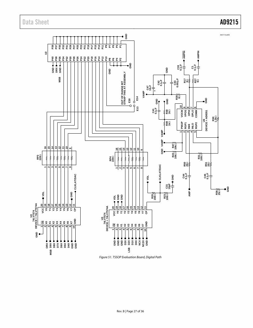
Figure 51. TSSOP Evaluation Board, Digital Path
AD9215 Data Sheet
Rev. B | Page 28 of 36
02874-A-050
+C
2710
F+
C25
10F
C24
0.1
FC
260.
1F
C37
0.00
1F
C38
0.00
1F
VDL
GN
DU
3/U
4 B
YPA
SSIN
G
+C
2010
FC
360.
1F
C39
0.00
1F
VCLK
GN
DU
5 B
YPA
SSIN
G
AVD
D B
YPA
SSIN
GG
ND
AVD
D
C48
0.1
FC
340.
1F
C35
0.00
1F
C49
0.00
1F
C51
0.1
F+
C50
10F
GN
DG
ND
DU
T B
YPA
SSIN
G
VCLK
+C
222
F
VDL
+C
1022
FDR
VDD
+C
410
FAVD
D
+C
322
FC
460.
1F
DR
VDD
GN
DD
UT
DR
VDD
BYP
ASS
ING
C21
0.1
FC
190.
001
F
1A 1B1Y
2A 2B2Y
3A 3B3Y
4A 4B4Y
PWR
GN
DEN
CO
DE
SCH
EMA
TIC
SH
OW
S 1-
GA
TE D
ELA
Y SE
TUP
FOR
TW
O-G
ATE
DEL
AY
REM
OVE
RES
ISTO
R R
52A
DD
RES
ISTO
RS
R38
AN
D R
18
OPT
ION
AL
EXTE
RN
AL
DA
TA R
EAD
Y
VCLK
DR
X
DR
X
DR
X
ENC
X
1 23
4 5
6
9 10
8
12 13
11 147
U5
74VC
X86
CLK
LAT/
DA
CJ3
GN
D
E52
E53
GN
DG
ND
GN
D
AVD
D
E51
E50
GN
D
E44
E43
VCLK
GN
D
VCLK
ENC
X
ENC
CLK
GN
DVC
LK
E36
E35
GN
D
ENC
VCLK
J4
GN
DG
ND
ENC
OD
E FR
OM
XO
RFO
R A
BU
FFER
ED E
NC
OD
E U
SE R
37FO
R A
DIR
ECT
ENC
OD
E U
SE R
35
R40
50
R41
1k
R42
1k
R39
1k
R26
1k
R2
1k
R43
1k
R52 0
R38 0
R18 0R25 0
R35 0R37 0
R14
50
C40
0.1
F
C28
0.1
F
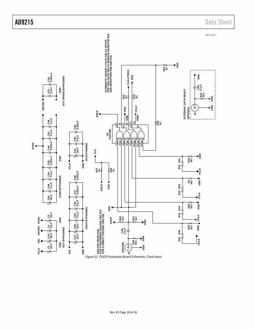
Figure 52. TSSOP Evaluation Board Schematic, Clock Input
Data Sheet AD9215
Rev. B | Page 29 of 36
0287
4-A
-051
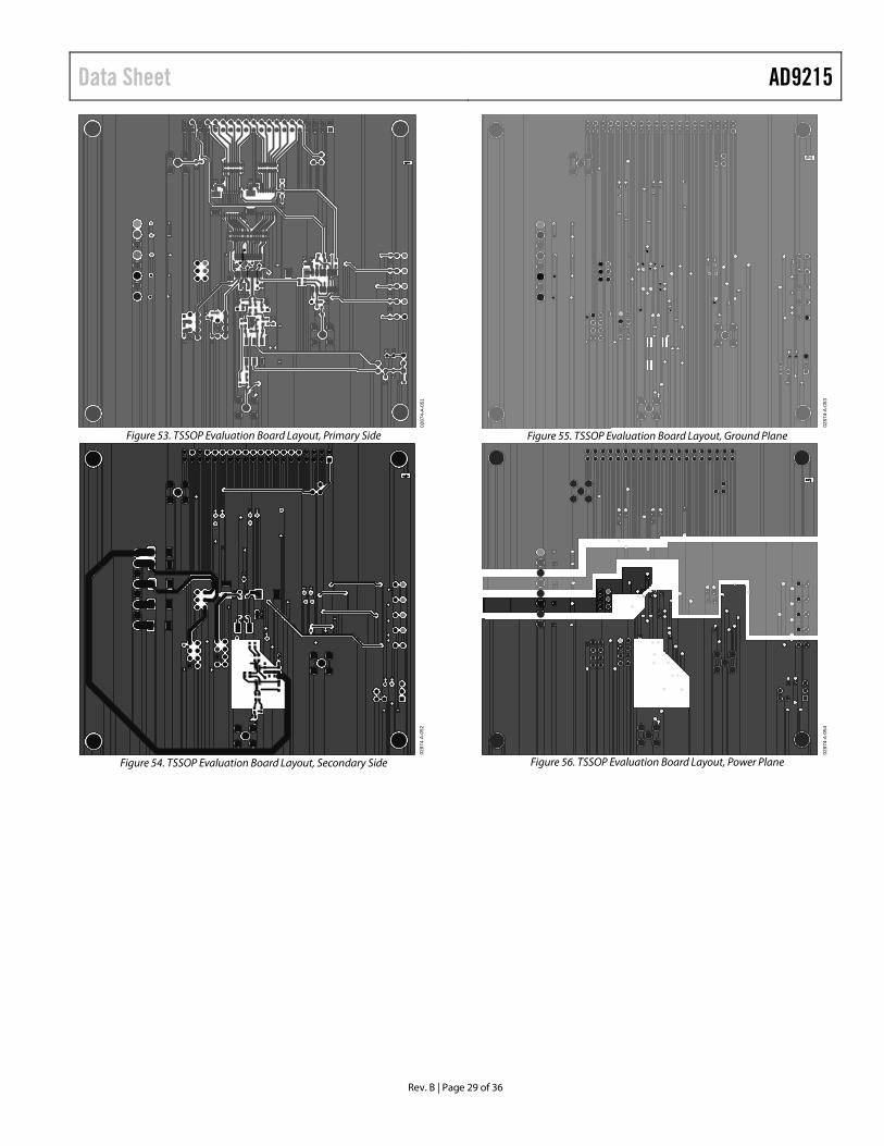
Figure 53. TSSOP Evaluation Board Layout, Primary Side
0287
4-A
-052
Figure 54. TSSOP Evaluation Board Layout, Secondary Side
0287
4-A
-053
Figure 55. TSSOP Evaluation Board Layout, Ground Plane
0287
4-A
-054
Figure 56. TSSOP Evaluation Board Layout, Power Plane

AD9215 Data Sheet
Rev. B | Page 30 of 36
0287
4-A
-055
Figure 57. TSSOP Evaluation Board Layout, Primary Silkscreen
0287
4-A
-056
Figure 58. TSSOP Evaluation Board Layout, Secondary Silkscreen
Data Sheet AD9215
Rev. B | Page 31 of 36
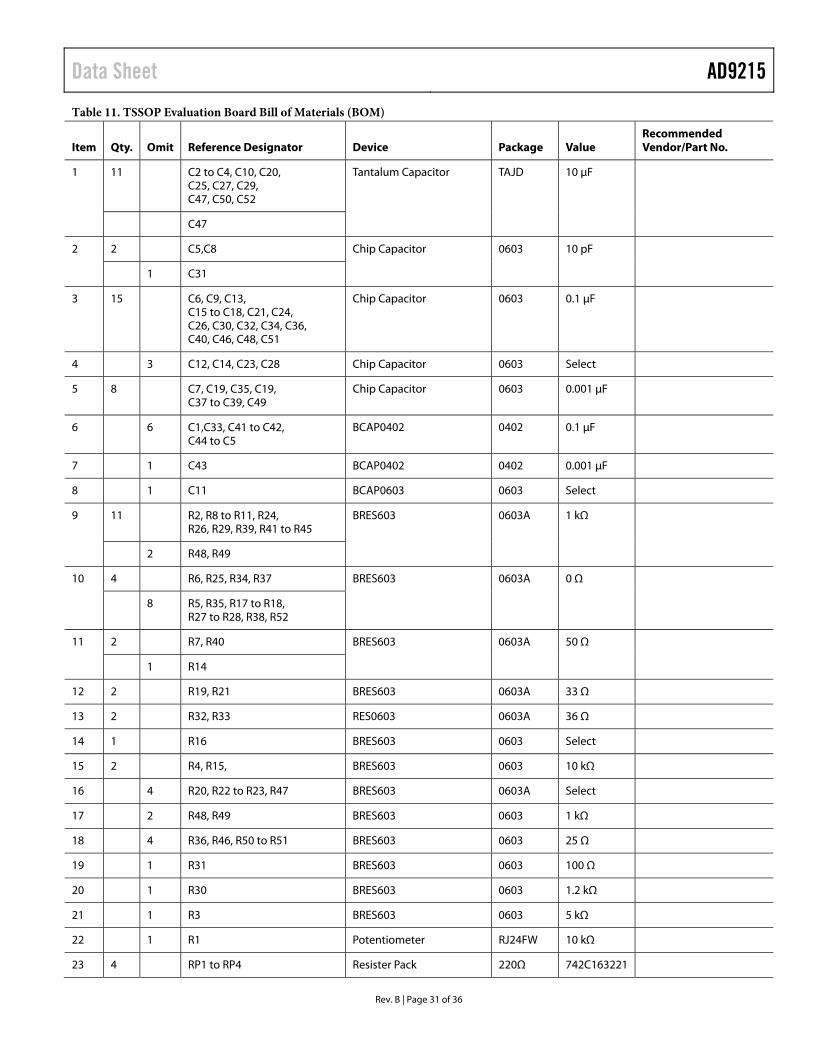
Table 11. TSSOP Evaluation Board Bill of Materials (BOM)
Item
Qty.
Omit
Reference Designator
Device
Package
Value
Recommended Vendor/Part No.
1 11 C2 to C4, C10, C20, C25, C27, C29, C47, C50, C52
Tantalum Capacitor TAJD 10 μF
C47
2 2 C5,C8 Chip Capacitor 0603 10 pF
1 C31
3 15 C6, C9, C13, C15 to C18, C21, C24, C26, C30, C32, C34, C36, C40, C46, C48, C51
Chip Capacitor 0603 0.1 μF
4 3 C12, C14, C23, C28 Chip Capacitor 0603 Select
5 8 C7, C19, C35, C19, C37 to C39, C49
Chip Capacitor 0603 0.001 μF
6 6 C1,C33, C41 to C42, C44 to C5
BCAP0402 0402 0.1 μF
7 1 C43 BCAP0402 0402 0.001 μF
8 1 C11 BCAP0603 0603 Select
9 11 R2, R8 to R11, R24, R26, R29, R39, R41 to R45
BRES603 0603A 1 kΩ
2 R48, R49
10 4 R6, R25, R34, R37 BRES603 0603A 0 Ω
8 R5, R35, R17 to R18, R27 to R28, R38, R52
11 2 R7, R40 BRES603 0603A 50 Ω
1 R14
12 2 R19, R21 BRES603 0603A 33 Ω
13 2 R32, R33 RES0603 0603A 36 Ω
14 1 R16 BRES603 0603 Select
15 2 R4, R15, BRES603 0603 10 kΩ
16 4 R20, R22 to R23, R47 BRES603 0603A Select
17 2 R48, R49 BRES603 0603 1 kΩ
18 4 R36, R46, R50 to R51 BRES603 0603 25 Ω
19 1 R31 BRES603 0603 100 Ω
20 1 R30 BRES603 0603 1.2 kΩ
21 1 R3 BRES603 0603 5 kΩ
22 1 R1 Potentiometer RJ24FW 10 kΩ
23 4 RP1 to RP4 Resister Pack 220Ω 742C163221
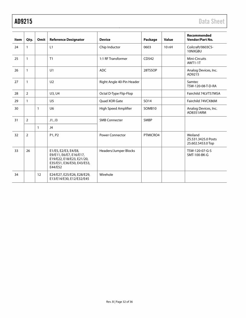
AD9215 Data Sheet
Rev. B | Page 32 of 36
Item
Qty.
Omit
Reference Designator
Device
Package
Value
Recommended Vendor/Part No.
24 1 L1 Chip Inductor 0603 10 nH Coilcraft/0603CS-10NXGBU
25 1 T1 1:1 RF Transformer CD542 Mini-Circuits AWT1-1T
26 1 U1 ADC 28TSSOP Analog Devices, Inc. AD9215
27 1 U2 Right Angle 40-Pin Header Samtec TSW-120-08-T-D-RA
28 2 U3, U4 Octal D-Type Flip-Flop Fairchild 74LVT57MSA
29 1 U5 Quad XOR Gate SO14 Fairchild 74VCX86M
30 1 U6 High Speed Amplifier SOMB10 Analog Devices, Inc. AD8351ARM
31 2 J1, J3 SMB Connecter SMBP
1 J4
32 2 P1, P2 Power Connector PTMICRO4 Weiland Z5.531.3425.0 Posts 25.602.5453.0 Top
33 26 E1/E5, E2/E3, E4/E8, E9/E11, E6/E7, E16/E17, E19/E22, E18/E23, E21/20, E35/E51, E36/E50, E43/E53, E44/E52
Headers/Jumper Blocks TSW-120-07-G-S SMT-100-BK-G
34 12 E24/E27, E25/E26, E28/E29, E13/E14/E30, E12/E32/E45
Wirehole

Data Sheet AD9215
Rev. B | Page 33 of 36
OUTLINE DIMENSIONS
COMPLIANT TO JEDEC STANDARDS MO-153-AE
2 8 1 5
1 41
8°0°SEATING
PLANECOPLANARITY
0.10
1.20 MAX
6.40 BSC
0.65BSC
PIN 1
0.300.19
0.200.09
4.504.404.30
0.750.600.45
9.809.709.60
0.150.05
Figure 59. 28-Lead Thin Shrink Small Outline Package [TSSOP]
(RU-28) Dimensions shown in millimeters
COMPLIANT TO JEDEC STANDARDS MO-220-WHHD. 1124
08-A
10.50BSC
BOTTOM VIEWTOP VIEW
PIN 1INDICATOR
32
916
17
24
25
8
EXPOSEDPAD
PIN 1INDICATOR
3.253.10 SQ2.95
SEATINGPLANE
0.05 MAX0.02 NOM
0.20 REF
COPLANARITY0.08
0.300.250.18
5.105.00 SQ4.90
0.800.750.70
FOR PROPER CONNECTION OFTHE EXPOSED PAD, REFER TOTHE PIN CONFIGURATION ANDFUNCTION DESCRIPTIONSSECTION OF THIS DATA SHEET.
0.500.400.30
0.25 MIN
Figure 60. 32-Lead Lead Frame Chip Scale Package [LFCSP_WQ]
5 mm × 5 mm Body, Very Very Thin Quad (CP-32-7)
Dimensions shown in millimeters

AD9215 Data Sheet
Rev. B | Page 34 of 36
ORDERING GUIDE Model1 Temperature Range Package Description Package Option AD9215BRUZ-65 −40°C to +85°C 28-Lead Thin Shrink Small Outline Package (TSSOP) RU-28 AD9215BRUZ-80 −40°C to +85°C 28-Lead Thin Shrink Small Outline Package (TSSOP) RU-28 AD9215BRUZ-105 −40°C to +85°C 28-Lead Thin Shrink Small Outline Package (TSSOP) RU-28 AD9215BRUZRL7-65 −40°C to +85°C 28-Lead Thin Shrink Small Outline Package (TSSOP) RU-28 AD9215BRUZRL7-80 −40°C to +85°C 28-Lead Thin Shrink Small Outline Package (TSSOP) RU-28 AD9215BRUZRL7-105 −40°C to +85°C 28-Lead Thin Shrink Small Outline Package (TSSOP) RU-28 AD9215BCPZ-65 −40°C to +85°C 32-Lead Lead Frame Chip Scale Package (LFCSP_WQ) CP-32-7 AD9215BCPZ-80 −40°C to +85°C 32-Lead Lead Frame Chip Scale Package (LFCSP_WQ) CP-32-7 AD9215BCPZ-105 −40°C to +85°C 32-Lead Lead Frame Chip Scale Package (LFCSP_WQ) CP-32-7
1 Z = RoHS Compliant Part.

Data Sheet AD9215
Rev. B | Page 35 of 36
NOTES

AD9215 Data Sheet
Rev. B | Page 36 of 36
NOTES
©2003–2013 Analog Devices, Inc. All rights reserved. Trademarks and registered trademarks are the property of their respective owners. D02874-0-2/13(B)