Embed Size (px)
Citation preview

14-Bit, 20 MSPS/40 MSPS/65 MSPS/80 MSPS, 3 V A/D Converter
Data Sheet AD9245
Rev. E Document Feedback Information furnished by Analog Devices is believed to be accurate and reliable. However, no responsibility is assumed by Analog Devices for its use, nor for any infringements of patents or other rights of third parties that may result from its use. Specifications subject to change without notice. No license is granted by implication or otherwise under any patent or patent rights of Analog Devices. Trademarks and registered trademarks are the property of their respective owners.
One Technology Way, P.O. Box 9106, Norwood, MA 02062-9106, U.S.A. Tel: 781.329.4700 ©2013 Analog Devices, Inc. All rights reserved. Technical Support www.analog.com
FEATURES Single 3 V supply operation (2.7 V to 3.6 V) SNR = 72.7 dBc to Nyquist SFDR = 83.0 dBc to Nyquist Low power
366 mW at 80 MSPS 300 mW at 65 MSPS 165 mW at 40 MSPS 90 mW at 20 MSPS
Differential input with 500 MHz bandwidth On-chip reference and sample-and-hold DNL = ±0.5 LSB Flexible analog input: 1 V p-p to 2 V p-p range Offset binary or twos complement data format Clock duty-cycle stabilizer
APPLICATIONS Medical imaging equipment IF sampling in communications receivers
WCDMA, CDMA-One, CDMA-2000, and TDS-CDMA Battery-powered instruments Hand-held scopemeters Spectrum analyzers Power-sensitive military applications
GENERAL DESCRIPTION
The AD9245 is a monolithic, single 3 V supply, 14-bit, 20 MSPS/40 MSPS/65 MSPS/80 MSPS analog-to-digital converter (ADC) featuring a high performance sample-and-hold amplifier (SHA) and voltage reference. The AD9245 uses a multistage differential pipelined architecture with output error correction logic to provide 14-bit accuracy and guarantee no missing codes over the full operating temperature range.
The wide bandwidth, truly differential SHA allows a variety of user-selectable input ranges and common modes, including single-ended applications. It is suitable for multiplexed systems that switch full-scale voltage levels in successive channels and for sampling single-channel inputs at frequencies well beyond the Nyquist rate. Combined with power and cost savings over previously available analog-to-digital converters, the AD9245 is suitable for applications in communications, imaging, and medical ultrasound.
FUNCTIONAL BLOCK DIAGRAM
0358
3-00
1
DRVDDAVDD
AGND
0.5V
CLK PDWN MODE DGND
OTR
VIN+
VIN–
REFT
REFB
AD9245
VREF
SENSE
SHA
A/D
MDAC1
4 16
14
3
A/D8-STAGE1 1/2-BIT PIPELINE
REFSELECT
CLOCKDUTY CYCLESTABILIZER
MODESELECT
CORRECTION LOGIC
OUTPUT BUFFERS
D13 (MSB)
D0 (LSB)
Figure 1.
A single-ended clock input is used to control all internal con-version cycles. A duty cycle stabilizer (DCS) compensates for wide variations in the clock duty cycle while maintaining excellent overall ADC performance. The digital output data is presented in straight binary or twos complement formats. An out-of-range (OTR) signal indicates an overflow condition that can be used with the most significant bit to determine low or high overflow. Fabricated on an advanced CMOS process, the AD9245 is available in a 32-lead LFCSP and is specified over the industrial temperature range (–40°C to +85°C).
PRODUCT HIGHLIGHTS 1. The AD9245 operates from a single 3 V power supply and
features a separate digital output driver supply to accommodate 2.5 V and 3.3 V logic families.
2. The patented SHA input maintains excellent performance for input frequencies up to 100 MHz and can be configured for single-ended or differential operation.
3. The AD9245 is pin-compatible with the AD9215, AD9235, and AD9236. This allows a simplified migration from 10 bits to 14 bits and 20 MSPS to 80 MSPS.
4. The clock DCS maintains overall ADC performance over a wide range of clock pulse widths.
5. The OTR output bit indicates when the signal is beyond the selected input range.
AD9245 Data Sheet
Rev. E | Page 2 of 32
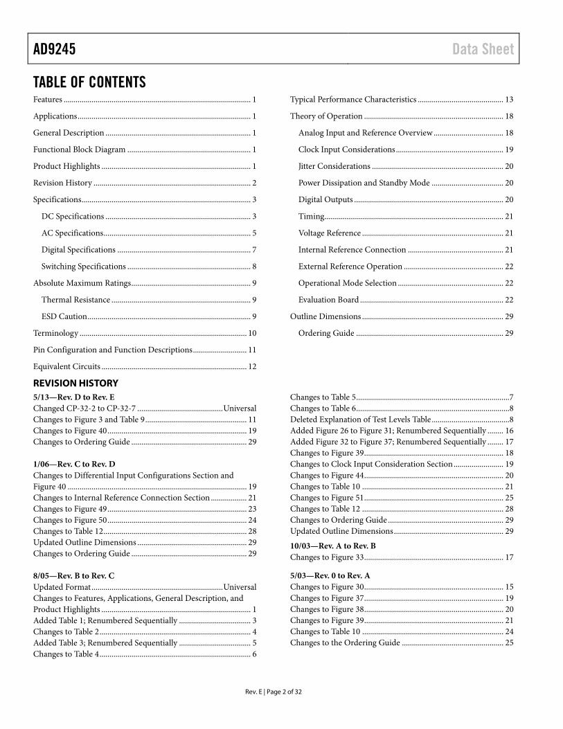
TABLE OF CONTENTS Features .............................................................................................. 1 Applications ....................................................................................... 1 General Description ......................................................................... 1 Functional Block Diagram .............................................................. 1 Product Highlights ........................................................................... 1 Revision History ............................................................................... 2 Specifications ..................................................................................... 3
DC Specifications ......................................................................... 3 AC Specifications .......................................................................... 5 Digital Specifications ................................................................... 7 Switching Specifications .............................................................. 8
Absolute Maximum Ratings ............................................................ 9 Thermal Resistance ...................................................................... 9 ESD Caution .................................................................................. 9
Terminology .................................................................................... 10 Pin Configuration and Function Descriptions ........................... 11 Equivalent Circuits ......................................................................... 12
Typical Performance Characteristics ........................................... 13 Theory of Operation ...................................................................... 18
Analog Input and Reference Overview ................................... 18 Clock Input Considerations ...................................................... 19 Jitter Considerations .................................................................. 20 Power Dissipation and Standby Mode .................................... 20 Digital Outputs ........................................................................... 20 Timing.......................................................................................... 21 Voltage Reference ....................................................................... 21 Internal Reference Connection ................................................ 21 External Reference Operation .................................................. 22 Operational Mode Selection ..................................................... 22 Evaluation Board ........................................................................ 22
Outline Dimensions ....................................................................... 29 Ordering Guide .......................................................................... 29
REVISION HISTORY 5/13—Rev. D to Rev. E Changed CP-32-2 to CP-32-7 ........................................... Universal Changes to Figure 3 and Table 9 ................................................... 11 Changes to Figure 40 ...................................................................... 19 Changes to Ordering Guide .......................................................... 29 1/06—Rev. C to Rev. D Changes to Differential Input Configurations Section and Figure 40 .......................................................................................... 19 Changes to Internal Reference Connection Section .................. 21 Changes to Figure 49 ...................................................................... 23 Changes to Figure 50 ...................................................................... 24 Changes to Table 12 ........................................................................ 28 Updated Outline Dimensions ....................................................... 29 Changes to Ordering Guide .......................................................... 29 8/05—Rev. B to Rev. C Updated Format .................................................................. Universal Changes to Features, Applications, General Description, and Product Highlights ........................................................................... 1 Added Table 1; Renumbered Sequentially .................................... 3 Changes to Table 2 ............................................................................ 4 Added Table 3; Renumbered Sequentially .................................... 5 Changes to Table 4 ............................................................................ 6
Changes to Table 5 ............................................................................. 7 Changes to Table 6 ............................................................................. 8 Deleted Explanation of Test Levels Table ....................................... 8 Added Figure 26 to Figure 31; Renumbered Sequentially ........ 16 Added Figure 32 to Figure 37; Renumbered Sequentially ........ 17 Changes to Figure 39 ...................................................................... 18 Changes to Clock Input Consideration Section ......................... 19 Changes to Figure 44 ...................................................................... 20 Changes to Table 10 ....................................................................... 21 Changes to Figure 51 ...................................................................... 25 Changes to Table 12 ....................................................................... 28 Changes to Ordering Guide .......................................................... 29 Updated Outline Dimensions ....................................................... 29
10/03—Rev. A to Rev. B Changes to Figure 33 ...................................................................... 17
5/03—Rev. 0 to Rev. A Changes to Figure 30 ...................................................................... 15 Changes to Figure 37 ...................................................................... 19 Changes to Figure 38 ...................................................................... 20 Changes to Figure 39 ...................................................................... 21 Changes to Table 10 ....................................................................... 24 Changes to the Ordering Guide ................................................... 25

Data Sheet AD9245
Rev. E | Page 3 of 32
SPECIFICATIONS DC SPECIFICATIONS AVDD = 3 V, DRVDD = 2.5 V, maximum sample rate, 2 V p-p differential input, 1.0 V internal reference, unless otherwise noted.
Table 1.
Parameter AD9245BCP-20 AD9245BCP-40 AD9245BCP-65
Unit Min Typ Max Min Typ Max Min Typ Max RESOLUTION 14 14 14 Bits ACCURACY
No Missing Codes Guaranteed 14 14 14 Bits Offset Error ±0.30 ±1.60 ±0.50 ±1.75 ±0.50 ±1.75 % FSR Gain Error1 ±0.30 ±3.25 ±0.50 ±3.25 ±0.50 ±6.90 % FSR Differential Nonlinearity (DNL)2 ±0.50 ±1.00 ±0.50 ±1.00 ±0.50 ±1.00 LSB Integral Nonlinearity (INL)2 ±1.20 ±3.10 ±1.40 ±3.40 ±1.60 ±5.55 LSB
TEMPERATURE DRIFT1 Offset Error ±2 ±2 ±3 ppm/°C Gain Error ±12 ±12 ±12 ppm/°C
INTERNAL VOLTAGE REFERENCE Output Voltage Error (1 V Mode) ±5 ±35 ±5 ±35 ±5 ±35 mV Load Regulation @ 1.0 mA 0.8 0.8 0.8 mV Output Voltage Error (0.5 V Mode) ±2.5 ±2.5 ±2.5 mV Load Regulation @ 0.5 mA 0.1 0.1 0.1 mV
INPUT REFERRED NOISE VREF = 0.5 V 2.28 2.28 2.28 LSB rms VREF = 1.0 V 1.08 1.08 1.08 LSB rms
ANALOG INPUT Input Span, VREF = 0.5 V 1 1 1 V p-p Input Span, VREF = 1.0 V 2 2 2 V p-p Input Capacitance3 7 7 7 pF
REFERENCE INPUT RESISTANCE 7 7 7 kΩ POWER SUPPLIES
Supply Voltages AVDD 2.7 3.0 3.6 2.7 3.0 3.6 2.7 3.0 3.6 V DRVDD 2.25 3.0 3.6 2.25 3.0 3.6 2.25 3.0 3.6 V
Supply Current IAVDD2 30 55 100 mA IDRVDD2 2 5 7 mA
PSRR ±0.01 ±0.01 ±0.01 % FSR POWER CONSUMPTION
DC Input4 90 165 300 mW Sine Wave Input2 95 120 180 220 320 375 mW Standby Power5 1.0 1.0 1.0 mW
1 Gain errors and gain temperature coefficients are based on the ADC only (with a fixed 1.0 V external reference). 2 Measured at maximum clock rate, low input frequency, full-scale sine wave, with approximately 5 pF loading on each output bit. 3 Input capacitance refers to the effective capacitance between one differential input pin and AGND. 4 Measured with dc input at maximum clock rate. 5 Standby power is measured with a dc input, the CLK pin inactive (that is, set to AVDD or AGND).

AD9245 Data Sheet
Rev. E | Page 4 of 32
AVDD = 3 V, DRVDD = 2.5 V, sample rate = 80 MSPS, 2 V p-p differential input, 1.0 V external reference, unless otherwise noted.
Table 2. AD9245BCP-80 Parameter Min Typ Max Unit RESOLUTION 14 Bits ACCURACY
No Missing Codes Guaranteed Offset Error1 ±0.30 ±1.2 % FSR Gain Error ±0.28 % FSR Gain Error1 ±0.70 ±4.16 % FSR Differential Nonlinearity (DNL)2 ±0.5 ±1.0 LSB Integral Nonlinearity (INL)2 ±1.4 ±5.15 LSB
TEMPERATURE DRIFT Offset Error1 ±10 ppm/°C Gain Error ±12 ppm/°C Gain Error1 ±17 ppm/°C
INTERNAL VOLTAGE REFERENCE Output Voltage Error (1 V Mode) ±3 ±34 mV Load Regulation @ 1.0 mA ±2 mV Output Voltage Error (0.5 V Mode) ±6 mV Load Regulation @ 0.5 mA ±1 mV
INPUT REFERRED NOISE VREF = 0.5 V 1.86 LSB rms VREF = 1.0 V 1.17 LSB rms
ANALOG INPUT Input Span, VREF = 0.5 V 1 V p-p Input Span, VREF = 1.0 V 2 V p-p Input Capacitance3 7 pF
REFERENCE INPUT RESISTANCE 7 kΩ POWER SUPPLIES
Supply Voltage AVDD 2.7 3.0 3.6 V DRVDD 2.25 2.5 3.6 V
Supply Current IAVDD2 122 138 mA IDRVDD2 9 mA
PSRR ±0.01 % FSR POWER CONSUMPTION
Low Frequency Input4 366 mW Standby Power5 1.0 mW
1 With a 1.0 V internal reference. 2 Measured at the maximum clock rate, low input frequency, full-scale sine wave, with approximately 5 pF loading on each output bit. 3 Input capacitance refers to the effective capacitance between one differential input pin and AGND. See Figure 4 for the equivalent analog input structure. 4 Measured at ac specification conditions without output drivers. 5 Standby power is measured with a dc input, CLK pin inactive (that is, set to AVDD or AGND).
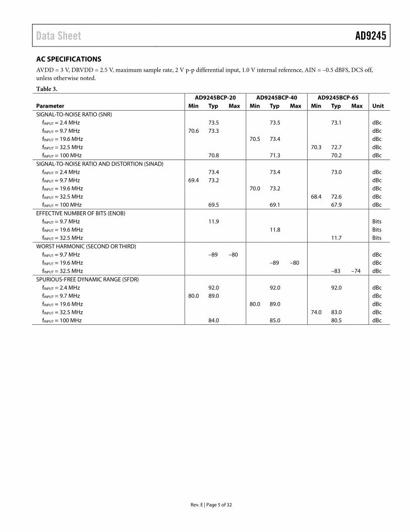
Data Sheet AD9245
Rev. E | Page 5 of 32
AC SPECIFICATIONS AVDD = 3 V, DRVDD = 2.5 V, maximum sample rate, 2 V p-p differential input, 1.0 V internal reference, AIN = –0.5 dBFS, DCS off, unless otherwise noted.
Table 3. AD9245BCP-20 AD9245BCP-40 AD9245BCP-65 Parameter Min Typ Max Min Typ Max Min Typ Max Unit SIGNAL-TO-NOISE RATIO (SNR)
fINPUT = 2.4 MHz 73.5 73.5 73.1 dBc fINPUT = 9.7 MHz 70.6 73.3 dBc fINPUT = 19.6 MHz 70.5 73.4 dBc fINPUT = 32.5 MHz 70.3 72.7 dBc fINPUT = 100 MHz 70.8 71.3 70.2 dBc
SIGNAL-TO-NOISE RATIO AND DISTORTION (SINAD) fINPUT = 2.4 MHz 73.4 73.4 73.0 dBc fINPUT = 9.7 MHz 69.4 73.2 dBc fINPUT = 19.6 MHz 70.0 73.2 dBc fINPUT = 32.5 MHz 68.4 72.6 dBc fINPUT = 100 MHz 69.5 69.1 67.9 dBc
EFFECTIVE NUMBER OF BITS (ENOB) fINPUT = 9.7 MHz 11.9 Bits fINPUT = 19.6 MHz 11.8 Bits fINPUT = 32.5 MHz 11.7 Bits
WORST HARMONIC (SECOND OR THIRD) fINPUT = 9.7 MHz –89 –80 dBc fINPUT = 19.6 MHz –89 –80 dBc fINPUT = 32.5 MHz –83 –74 dBc
SPURIOUS-FREE DYNAMIC RANGE (SFDR) fINPUT = 2.4 MHz 92.0 92.0 92.0 dBc fINPUT = 9.7 MHz 80.0 89.0 dBc fINPUT = 19.6 MHz 80.0 89.0 dBc fINPUT = 32.5 MHz 74.0 83.0 dBc fINPUT = 100 MHz 84.0 85.0 80.5 dBc

AD9245 Data Sheet
Rev. E | Page 6 of 32
AVDD = 3 V, DRVDD = 2.5 V, sample rate = 80 MSPS, 2 V p-p differential input, 1.0 V external reference, AIN = –0.5 dBFS, DCS off, unless otherwise noted.
Table 4. AD9245BCP-80 Parameter Min Typ Max Unit SIGNAL-TO-NOISE RATIO (SNR)
fIN = 2.4 MHz 71.1 73.3 dB fIN = 40 MHz 72.7 dB fIN = 70 MHz 70.5 71.7 dB fIN = 100 MHz 70.2 dB
SIGNAL-TO-NOISE AND DISTORTION (SINAD) fIN = 2.4 MHz 70.7 73.2 dB fIN = 40 MHz 72.5 dB fIN = 70 MHz 69.9 71.2 dB fIN = 100 MHz 69.6 dB
EFFECTIVE NUMBER OF BITS (ENOB) fIN = 2.4 MHz 11.5 11.9 Bits fIN = 40 MHz 11.8 Bits fIN = 70 MHz 11.3 11.5 Bits fIN = 100 MHz 11.3 Bits
WORST HARMONIC (SECOND OR THIRD) fIN = 2.4 MHz −92.8 –76.5 dBc fIN = 40 MHz –87.6 dBc fIN = 70 MHz −81.6 –75.7 dBc fIN = 100 MHz –79.0 dBc
SPURIOUS-FREE DYNAMIC RANGE (SFDR) fIN = 2.4 MHz 76.5 92.8 dBc fIN = 40 MHz 87.6 dBc fIN = 70 MHz 75.7 81.6 dBc fIN = 100 MHz 79.0 dBc
Data Sheet AD9245
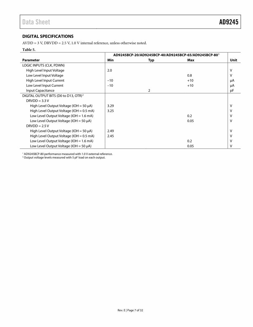
Rev. E | Page 7 of 32
DIGITAL SPECIFICATIONS AVDD = 3 V, DRVDD = 2.5 V, 1.0 V internal reference, unless otherwise noted.
Table 5. AD9245BCP-20/AD9245BCP-40/AD9245BCP-65/AD9245BCP-801 Parameter Min Typ Max Unit LOGIC INPUTS (CLK, PDWN)
High Level Input Voltage 2.0 V Low Level Input Voltage 0.8 V High Level Input Current –10 +10 µA Low Level Input Current –10 +10 µA Input Capacitance 2 pF
DIGITAL OUTPUT BITS (D0 to D13, OTR)2 DRVDD = 3.3 V
High Level Output Voltage (IOH = 50 µA) 3.29 V High Level Output Voltage (IOH = 0.5 mA) 3.25 V Low Level Output Voltage (IOH = 1.6 mA) 0.2 V Low Level Output Voltage (IOH = 50 µA) 0.05 V
DRVDD = 2.5 V High Level Output Voltage (IOH = 50 µA) 2.49 V High Level Output Voltage (IOH = 0.5 mA) 2.45 V Low Level Output Voltage (IOH = 1.6 mA) 0.2 V Low Level Output Voltage (IOH = 50 µA) 0.05 V
1 AD9245BCP-80 performance measured with 1.0 V external reference. 2 Output voltage levels measured with 5 pF load on each output.

AD9245 Data Sheet
Rev. E | Page 8 of 32
SWITCHING SPECIFICATIONS AVDD = 3 V, DRVDD = 2.5 V, unless otherwise noted.
Table 6.
Parameter AD9245BCP-20 AD9245BCP-40 AD9245BCP-65 AD9245BCP-80 Unit
Min Typ Max Min Typ Max Min Typ Max Min Typ Max
CLOCK INPUT PARAMETERS Maximum Conversion Rate 20 40 65 80 MSPS Minimum Conversion Rate 1 1 1 1 MSPS CLK Period 50.0 25.0 15.4 12.5 ns CLK Pulse Width High1 15.0 8.8 6.2 4.6 ns CLK Pulse Width Low1 15.0 8.8 6.2 4.6 ns
DATA OUTPUT PARAMETERS Output Delay2 (tPD) 3.5 3.5 3.5 4.2 ns Pipeline Delay (Latency) 7 7 7 7 Cycles Aperture Delay (tA) 1.0 1.0 1.0 1.0 ns Aperture Uncertainty Jitter (tJ) 0.5 0.5 0.5 0.3 ps rms Wake-Up Time3 3.0 3.0 3.0 7.0 ms
OUT-OF-RANGE RECOVERY TIME 1 1 2 2 Cycles 1 For the AD9245BCP-65 and AD9245BCP-80 models only, with duty cycle stabilizer enabled. DCS function not applicable for AD9245BCP-20 and AD9245BCP-40
models. 2 Output delay is measured from CLK 50% transition to DATA 50% transition, with 5 pF load on each output. 3 Wake-up time is dependent on value of decoupling capacitors; typical values shown with 0.1 μF and 10 μF capacitors on REFT and REFB.
tA
2.0ns MINtPD = 6.0ns MAX
0358
3-00
2N–9 N–8 N–7 N–6 N–5 N–4 N–3 N–2 N–1 N
ANALOGINPUT
CLK
DATAOUT
N–1
NN+1
N+2
N+3
N+4N+5 N+6
N+7
N+8
Figure 2. Timing Diagram

Data Sheet AD9245
Rev. E | Page 9 of 32
ABSOLUTE MAXIMUM RATINGS
Table 7. Parameter With Respect to Min Max Unit ELECTRICAL
AVDD AGND –0.3 +3.9 V DRVDD DGND –0.3 +3.9 V AGND DGND –0.3 +0.3 V AVDD DRVDD –3.9 +3.9 V D0 to D13 DGND –0.3 DRVDD + 0.3 V CLK, MODE AGND –0.3 AVDD + 0.3 V VIN+, VIN– AGND –0.3 AVDD + 0.3 V VREF AGND –0.3 AVDD + 0.3 V SENSE AGND –0.3 AVDD + 0.3 V REFT, REFB AGND –0.3 AVDD + 0.3 V PDWN AGND –0.3 AVDD + 0.3 V
ENVIRONMENTAL
Storage Temperature Range –65 +125 °C Operating Temperature Range –40 +85 °C Lead Temperature (Soldering 10 sec)
300 °C
Junction Temperature 150 °C
Stresses above those listed under Absolute Maximum Ratings may cause permanent damage to the device. This is a stress rating only; functional operation of the device at these or any other conditions above those indicated in the operational section of this specification is not implied. Exposure to absolute maximum rating conditions for extended periods may affect device reliability.
THERMAL RESISTANCE θJA is specified for the worst-case conditions on a 4-layer board in still air, in accordance with EIA/JESD51-1.
Table 8. Thermal Resistance Package Type θJA θJC Unit
32-Lead LFCSP 32.5 32.71 °C/W
Airflow increases heat dissipation, effectively reducing θJA. In addition, more metal directly in contact with the package leads from metal traces, through holes, ground, and power planes reduces the θJA. It is recommended that the exposed paddle be soldered to the ground plane for the LFCSP package. There is an increased reliability of the solder joints, and maximum thermal capability of the package is achieved with the exposed paddle soldered to the customer board.
ESD CAUTION ESD (electrostatic discharge) sensitive device. Electrostatic charges as high as 4000 V readily accumulate on the human body and test equipment and can discharge without detection. Although this product features proprietary ESD protection circuitry, permanent damage may occur on devices subjected to high energy electrostatic discharges. Therefore, proper ESD precautions are recommended to avoid performance degradation or loss of functionality.
AD9245 Data Sheet
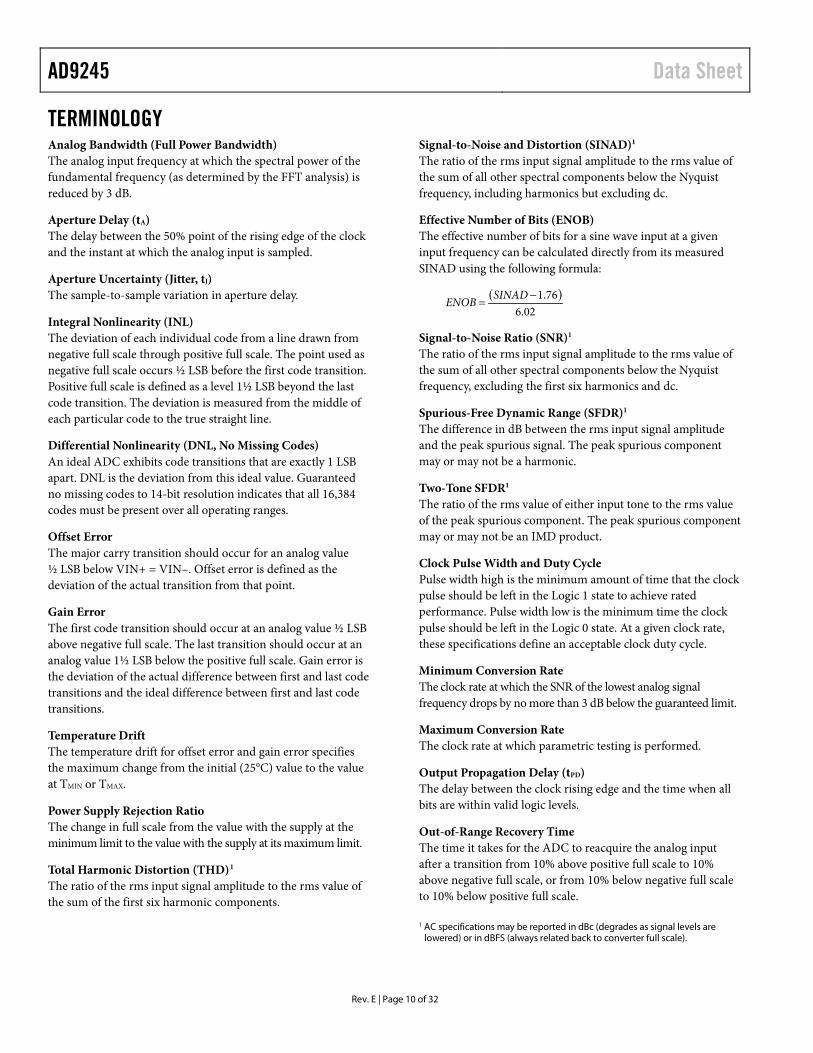
Rev. E | Page 10 of 32
TERMINOLOGY Analog Bandwidth (Full Power Bandwidth) The analog input frequency at which the spectral power of the fundamental frequency (as determined by the FFT analysis) is reduced by 3 dB.
Aperture Delay (tA) The delay between the 50% point of the rising edge of the clock and the instant at which the analog input is sampled.
Aperture Uncertainty (Jitter, tJ) The sample-to-sample variation in aperture delay.
Integral Nonlinearity (INL) The deviation of each individual code from a line drawn from negative full scale through positive full scale. The point used as negative full scale occurs ½ LSB before the first code transition. Positive full scale is defined as a level 1½ LSB beyond the last code transition. The deviation is measured from the middle of each particular code to the true straight line.
Differential Nonlinearity (DNL, No Missing Codes) An ideal ADC exhibits code transitions that are exactly 1 LSB apart. DNL is the deviation from this ideal value. Guaranteed no missing codes to 14-bit resolution indicates that all 16,384 codes must be present over all operating ranges.
Offset Error The major carry transition should occur for an analog value ½ LSB below VIN+ = VIN–. Offset error is defined as the deviation of the actual transition from that point.
Gain Error The first code transition should occur at an analog value ½ LSB above negative full scale. The last transition should occur at an analog value 1½ LSB below the positive full scale. Gain error is the deviation of the actual difference between first and last code transitions and the ideal difference between first and last code transitions.
Temperature Drift The temperature drift for offset error and gain error specifies the maximum change from the initial (25°C) value to the value at TMIN or TMAX.
Power Supply Rejection Ratio The change in full scale from the value with the supply at the minimum limit to the value with the supply at its maximum limit.
Total Harmonic Distortion (THD)1 The ratio of the rms input signal amplitude to the rms value of the sum of the first six harmonic components.
Signal-to-Noise and Distortion (SINAD)1
The ratio of the rms input signal amplitude to the rms value of the sum of all other spectral components below the Nyquist frequency, including harmonics but excluding dc.
Effective Number of Bits (ENOB) The effective number of bits for a sine wave input at a given input frequency can be calculated directly from its measured SINAD using the following formula:
( )6.02
1.76−=
SINADENOB
Signal-to-Noise Ratio (SNR)1
The ratio of the rms input signal amplitude to the rms value of the sum of all other spectral components below the Nyquist frequency, excluding the first six harmonics and dc.
Spurious-Free Dynamic Range (SFDR)1
The difference in dB between the rms input signal amplitude and the peak spurious signal. The peak spurious component may or may not be a harmonic.
Two-Tone SFDR1
The ratio of the rms value of either input tone to the rms value of the peak spurious component. The peak spurious component may or may not be an IMD product.
Clock Pulse Width and Duty Cycle Pulse width high is the minimum amount of time that the clock pulse should be left in the Logic 1 state to achieve rated performance. Pulse width low is the minimum time the clock pulse should be left in the Logic 0 state. At a given clock rate, these specifications define an acceptable clock duty cycle.
Minimum Conversion Rate The clock rate at which the SNR of the lowest analog signal frequency drops by no more than 3 dB below the guaranteed limit.
Maximum Conversion Rate The clock rate at which parametric testing is performed.
Output Propagation Delay (tPD) The delay between the clock rising edge and the time when all bits are within valid logic levels.
Out-of-Range Recovery Time The time it takes for the ADC to reacquire the analog input after a transition from 10% above positive full scale to 10% above negative full scale, or from 10% below negative full scale to 10% below positive full scale. 1 AC specifications may be reported in dBc (degrades as signal levels are
lowered) or in dBFS (always related back to converter full scale).

Data Sheet AD9245
Rev. E | Page 11 of 32
PIN CONFIGURATION AND FUNCTION DESCRIPTIONS
VREFSENSEMODEOTRD13 (MSB)D12D11
D1(LSB) D0
PDWN
D3D2
D9
D8
D7
D6
D5
D4
DG
ND
DR
VD
D
AV
DD
AG
ND
VIN
–V
IN+
AG
ND
AV
DD
RE
FT
RE
FB
DNCCLKDNC
D10
NOTES1. DNC = DO NOT CONNECT. DO NOT CONNECT TO THIS PIN.2. IT IS RECOMMENDED THAT THE EXPOSED PADDLE BE SOLDERED TO THE GROUND PLANE FOR THE LFCSP PACKAGE. THERE IS AN INCREASED RELIABILITY OF THE SOLDER JOINTS, AND THE MAXIMUM THERMAL CAPABILITY OF THE PACKAGE IS ACHIEVED WITH THE EXPOSED PADDLE SOLDERED TO THE CUSTOMER BOARD. 03
583-
022
2423222120191817
12345678
9 10 11 12 13 14 15 16
32 31 30 29 28 27 26 25
AD9245TOP VIEW
(Not to Scale)
Figure 3. LFCSP Pin Configuration
Table 9. Pin Function Descriptions Pin No. Mnemonic Description 1, 3 DNC Do Not Connect 2 CLK Clock Input Pin 4 PDWN Power-Down Function Select 5 to 14, 17 to 20 D0 (LSB) to D13 (MSB) Data Output Bits 15 DGND Digital Output Ground 16 DRVDD Digital Output Driver Supply 21 OTR Out-of-Range Indicator 22 MODE Data Format Select and DCS Mode Selection (See Table 11) 23 SENSE Reference Mode Selection (See Table 10) 24 VREF Voltage Reference Input/Output 25 REFB Differential Reference (–) 26 REFT Differential Reference (+) 27, 32 AVDD Analog Power Supply 28, 31 AGND Analog Ground 29 VIN+ Analog Input Pin (+) 30 VIN– Analog Input Pin (–) EPAD Exposed Pad. It is recommended that the exposed paddle be soldered to the ground
plane for the LFCSP package. There is an increased reliability of the solder joints, and the maximum thermal capability of the package is achieved with the exposed paddle soldered to the customer board.

AD9245 Data Sheet
Rev. E | Page 12 of 32
EQUIVALENT CIRCUITS
AVDD
VIN+, VIN–
0358
3-00
3
Figure 4. Equivalent Analog Input Circuit
03
583-
004
AVDD
MODE
20k
Figure 5. Equivalent MODE Input Circuit
D13-D0,OTR
DRVDD
0358
3-00
5
Figure 6. Equivalent Digital Output Circuit
0358
3-00
6
AVDD
CLK,PDWN
Figure 7. Equivalent Digital Input Circuit

Data Sheet AD9245
Rev. E | Page 13 of 32
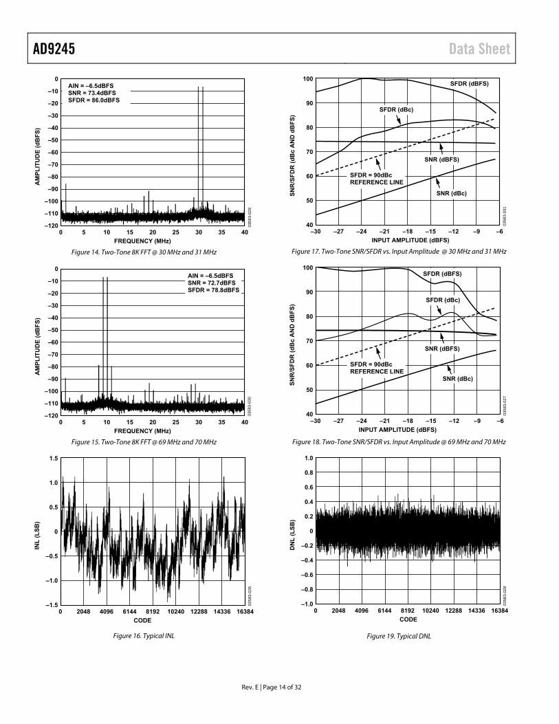
TYPICAL PERFORMANCE CHARACTERISTICS DUT = AD9245-80, AVDD = 3.0 V, DRVDD = 2.5 V, maximum sample rate, DCS disabled, TA = 25°C, 2 V p-p differential input, AIN = −0.5 dBFS, VREF = 1.0 V external, unless otherwise noted.
FREQUENCY (MHz)
AM
PL
ITU
DE
(d
BF
S)
0 5 10 15 20 25 30 35–120
0
–10
–20
–30
–40
–50
–60
–70
–80
–90
–100
–110
40
0358
3-03
2
AIN = –0.5dBFSSNR = 73.2dBcENOB = 11.8 BITSSFDR = 92.8dBc
Figure 8. Single Tone 8K FFT @ 2.5 MHz
FREQUENCY (MHz)
AM
PL
ITU
DE
(d
BF
S)
0 5 10 15 20 25 30 35–120
0
–10
–20
–30
–40
–50
–60
–70
–80
–90
–100
–110
40
0358
3-02
3
AIN = –0.5dBFSSNR = 72.7dBcENOB = 11.8 BITSSFDR = 87.6dBc
Figure 9. Single Tone 8K FFT @ 39 MHz
FREQUENCY (MHz)
AM
PL
ITU
DE
(d
BF
S)
0 5 10 15 20 25 30 35–120
0
–10
–20
–30
–40
–50
–60
–70
–80
–90
–100
–110
40
0358
3-02
4
AIN = –0.5dBFSSNR = 71.7dBcENOB = 11.5 BITSSFDR = 81.6dBc
Figure 10. Single Tone 8K FFT @ 70 MHz
INPUT AMPLITUDE (dBFS)
SN
R/S
FD
R (
dB
c A
ND
dB
FS
)
–30 –25 –20 –15 –10 –540
50
60
70
80
90
100
0
0358
3-03
3
SFDR (dBFS)
SNR (dBc)
SFDR = 90dBcREFERENCE LINE
SFDR (dBc)
SNR (dBFS)
Figure 11. Single Tone SNR/SFDR vs. Input Amplitude (AIN) @ 2.5 MHz
INPUT AMPLITUDE (dBFS)
SN
R/S
FD
R (
dB
c A
ND
dB
FS
)
–30 –25 –20 –15 –10 –540
50
60
70
80
90
100
0
0358
3-03
4
SFDR (dBFS)
SNR (dBc)
SFDR = 90dBcREFERENCE LINE
SFDR (dBc)
SNR (dBFS)
Figure 12. Single Tone SNR/SFDR vs. Input Amplitude (AIN) @ 39 MHz
SAMPLE RATE (MSPS)
SN
R/S
FD
R (
dB
c)
0 20 40 60 8050
60
70
80
90
100
100
0358
3-02
5
SFDR (DIFF)
SFDR (SE) SNR (DIFF)
SNR (SE)
Figure 13. SNR/SFDR vs. Sample Rate @ 40 MHz
AD9245 Data Sheet
Rev. E | Page 14 of 32
FREQUENCY (MHz)
AM
PL
ITU
DE
(d
BF
S)
0 5 10 15 20 25 30 35–120
–110
–100
–90
–80
–70
–60
–50
–40
–30
–20
–10
0
40
0358
3-02
9
AIN = –6.5dBFSSNR = 73.4dBFSSFDR = 86.0dBFS
Figure 14. Two-Tone 8K FFT @ 30 MHz and 31 MHz
FREQUENCY (MHz)
AM
PL
ITU
DE
(d
BF
S)
0 5 10 15 20 25 30 35–120
–110
–100
–90
–80
–70
–60
–50
–40
–30
–20
–10
0
40
0358
3-03
0
AIN = –6.5dBFSSNR = 72.7dBFSSFDR = 78.8dBFS
Figure 15. Two-Tone 8K FFT @ 69 MHz and 70 MHz
CODE
INL
(L
SB
)
0 2048 4096 6144 8192 10240 12288 14336–1.5
1.5
1.0
0.5
0
–0.5
–1.0
16384
0358
3-02
6
Figure 16. Typical INL
INPUT AMPLITUDE (dBFS)
SN
R/S
FD
R (
dB
c A
ND
dB
FS
)
–30 –27 –24 –21 –18 –15 –12 –940
100
90
80
70
60
50
–6
0358
3-03
1
SFDR = 90dBcREFERENCE LINE
SFDR (dBFS)
SFDR (dBc)
SNR (dBFS)
SNR (dBc)
Figure 17. Two-Tone SNR/SFDR vs. Input Amplitude @ 30 MHz and 31 MHz
INPUT AMPLITUDE (dBFS)
SN
R/S
FD
R (
dB
c A
ND
dB
FS
)
–30 –27 –24 –21 –18 –15 –12 –940
100
90
80
70
60
50
–6
0358
3-02
7
SFDR = 90dBcREFERENCE LINE
SFDR (dBFS)
SFDR (dBc)
SNR (dBFS)
SNR (dBc)
Figure 18. Two-Tone SNR/SFDR vs. Input Amplitude @ 69 MHz and 70 MHz
CODE
DN
L (
LS
B)
0 2048 4096 6144 8192 10240 12288 14336–1.0
1.0
–0.8
–0.6
–0.4
–0.2
0
0.2
0.4
0.6
0.8
16384
0358
3-02
8
Figure 19. Typical DNL
Data Sheet AD9245
Rev. E | Page 15 of 32
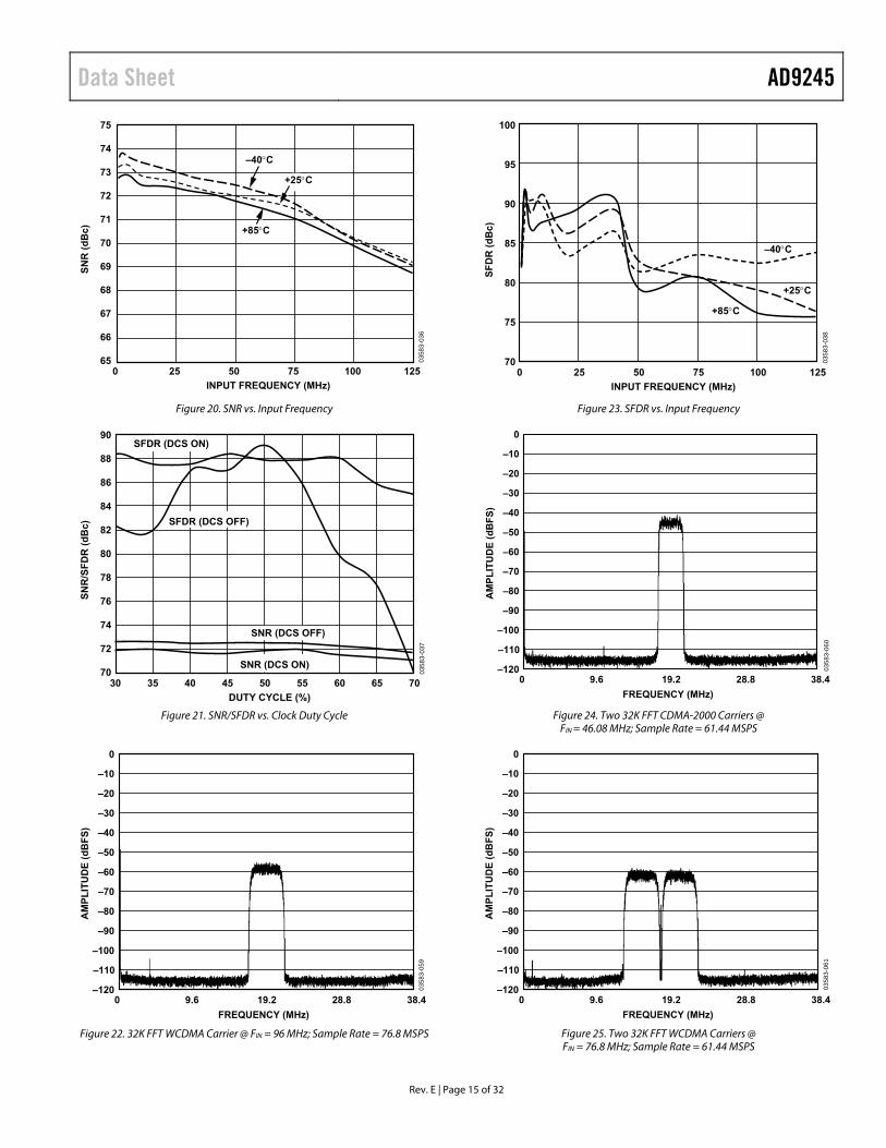
INPUT FREQUENCY (MHz)
SN
R (
dB
c)
0 25 50 75 10065
75
–40C
+85C
74
73
72
71
70
69
68
67
66
125
0358
3-03
6
+25C
Figure 20. SNR vs. Input Frequency
DUTY CYCLE (%)
SN
R/S
FD
R (
dB
c)
30 35 40 45 50 55 60 6570
90
88
86
84
82
80
78
76
74
72
70
0358
3-03
7
SNR (DCS ON)
SNR (DCS OFF)
SFDR (DCS ON)
SFDR (DCS OFF)
Figure 21. SNR/SFDR vs. Clock Duty Cycle
0
–10
–20
–30
–40
–50
–60
–70
–80
–90
–100
–110
AM
PL
ITU
DE
(d
BF
S)
–1200 9.6 19.2 28.8 38.4
FREQUENCY (MHz)
0358
3-05
9
Figure 22. 32K FFT WCDMA Carrier @ FIN = 96 MHz; Sample Rate = 76.8 MSPS
INPUT FREQUENCY (MHz)
SF
DR
(d
Bc)
0 25 50 75 10070
100
95
90
85
80
75
125
–40C
+25C
+85C
0358
3-03
8
Figure 23. SFDR vs. Input Frequency
0
–10
–20
–30
–40
–50
–60
–70
–80
–90
–100
–110
AM
PL
ITU
DE
(d
BF
S)
–1200 9.6 19.2 28.8 38.4
FREQUENCY (MHz)
0358
3-06
0
Figure 24. Two 32K FFT CDMA-2000 Carriers @ FIN = 46.08 MHz; Sample Rate = 61.44 MSPS
0
–10
–20
–30
–40
–50
–60
–70
–80
–90
–100
–110
AM
PL
ITU
DE
(d
BF
S)
–1200 9.6 19.2 28.8 38.4
FREQUENCY (MHz)
0358
3-06
1
Figure 25. Two 32K FFT WCDMA Carriers @ FIN = 76.8 MHz; Sample Rate = 61.44 MSPS
AD9245 Data Sheet
Rev. E | Page 16 of 32
0
–20
–40
–60
–80
–100
–120
AM
PLIT
UD
E (d
BFS
)
0 5 10 15 20 25 30FREQUENCY (MHz)
0358
3-06
2
AIN = –0.5dBFSSNR = 72.7dBcENOB = 11.7 BITSSFDR = 81.3dBc
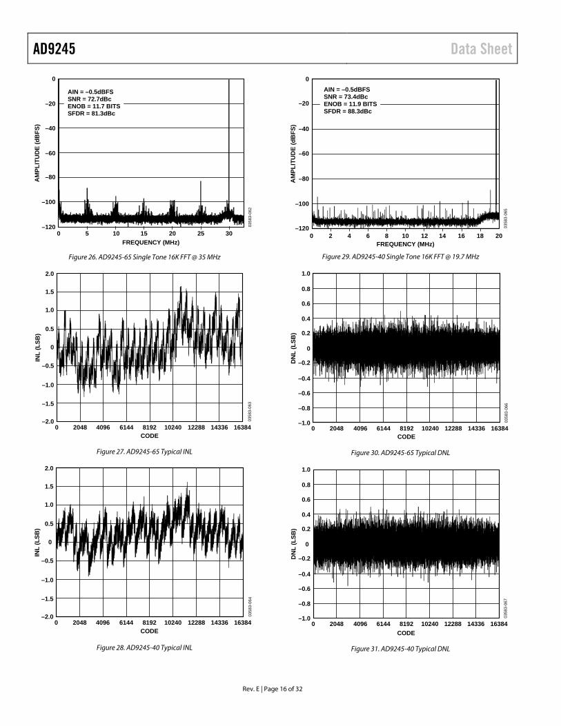
Figure 26. AD9245-65 Single Tone 16K FFT @ 35 MHz
2.0
1.5
1.0
0.5
0
–0.5
–1.0
–1.5
–2.0
INL
(LSB
)
0358
3-06
3
0 2048 4096 6144 8192 10240 12288 14336 16384CODE
Figure 27. AD9245-65 Typical INL
2.0
1.5
1.0
0.5
0
–0.5
–1.0
–1.5
–2.0
INL
(LSB
)
0358
3-06
4
0 2048 4096 6144 8192 10240 12288 14336 16384CODE
Figure 28. AD9245-40 Typical INL
0
–20
–40
–60
–80
–100
–120
AM
PLIT
UD
E (d
BFS
)
0 2 4 6 8 10 12 14 16 18 20FREQUENCY (MHz)
0358
3-06
5
AIN = –0.5dBFSSNR = 73.4dBcENOB = 11.9 BITSSFDR = 88.3dBc
Figure 29. AD9245-40 Single Tone 16K FFT @ 19.7 MHz
1.0
0.8
0.6
0.4
0.2
0
–0.2
–0.4
–0.6
–0.8
–1.0
DN
L (L
SB)
0 2048 4096 6144 8192 10240 12288 14336 16384CODE
0358
3-06
6
Figure 30. AD9245-65 Typical DNL
1.0
0.8
0.6
0.4
0.2
0
–0.2
–0.4
–0.6
–0.8
–1.0
DN
L (L
SB)
0 2048 4096 6144 8192 10240 12288 14336 16384CODE
0358
3-06
7
Figure 31. AD9245-40 Typical DNL

Data Sheet AD9245
Rev. E | Page 17 of 32
2.0
1.5
1.0
0.5
0
–0.5
–1.0
–1.5
–2.0
INL
(LSB
)
0 2048 4096 6144 8192 10240 12288 14336 16384CODE
Figure 32. AD9245-20 Typical INL
0
–20
–40
–60
–80
–100
–120
AM
PLIT
UD
E (d
BFS
)
0 1 2 3 4 5 6 7 8 9 10FREQUENCY (MHz)
AIN = –0.5dBFSSNR = 73.4dBcENOB = 11.9 BITSSFDR = 95.0dBc
0358
3-06
9
Figure 33. AD9245-20 Single Tone 16K FFT @ 5 MHz
75
70
65
60
55
50
SIN
AD
(dB
c)
1 10 100INPUT FREQUENCY (MHz)
0358
3-07
0
–0.5dBFS
–6dBFS
–20dBFS
Figure 34. AD9245-20 SINAD vs. Input Frequency
1.0
0.8
0.6
0.4
0.2
0
–0.2
–0.4
–0.6
–0.8
–1.0
DN
L (L
SB)
0 2048 4096 6144 8192 10240 12288 14336 16384CODE
0358
3-07
1
Figure 35. AD9245-20 Typical DNL
0
–20
–40
–60
–80
–100
–120
AM
PLIT
UD
E (d
BFS
)
0 1 2 3 4 5 6 7 8 9 10FREQUENCY (MHz)
0358
3-07
2
AIN = –0.5dBFSSNR = 73.3dBcENOB = 11.9 BITSSFDR = 92.6dBc
Figure 36. AD9245-20 Single Tone 16K FFT @ 9.7 MHz
HIT
S
N–3 N–2 N–1 N N+1 N+2 N+3CODE
0358
3-07
3
253625
1755666
72816247996189
3167101
547498
10004707
Figure 37. AD9245-20 Grounded-Input Histogram

AD9245 Data Sheet
Rev. E | Page 18 of 32
THEORY OF OPERATION The AD9245 architecture consists of a front-end sample-and-hold amplifier (SHA) followed by a pipelined switched capacitor ADC. The pipelined ADC is divided into three sections consisting of a 4-bit first stage followed by eight 1.5-bit stages, and a final 3-bit flash. Each stage provides sufficient overlap to correct for flash errors in the preceding stages. The quantized outputs from each stage are combined into a final 14-bit result in the digital correction logic. The pipelined architecture permits the first stage to operate on a new input sample, while the remaining stages operate on preceding samples. Sampling occurs on the rising edge of the clock.
Each stage of the pipeline, excluding the last, consists of a low resolution flash ADC connected to a switched capacitor DAC and interstage residue amplifier (MDAC). The residue amplifier magnifies the difference between the reconstructed DAC output and the flash input for the next stage in the pipeline. One bit of redundancy is used in each stage to facilitate digital correction of flash errors. The last stage simply consists of a flash ADC.
The input stage contains a differential SHA that can be ac-coupled or dc-coupled in differential or single-ended modes. The output staging block aligns the data, carries out the error correction, and passes the data to the output buffers. The output buffers are powered from a separate supply, allowing adjustment of the output voltage swing. During power-down, the output buffers go into a high impedance state.
ANALOG INPUT AND REFERENCE OVERVIEW The analog input to the AD9245 is a differential switched-capacitor SHA that has been designed for optimum performance while processing a differential input signal. The SHA input can support a wide common-mode range (VCM) and maintain excellent performance, as shown in Figure 38. An input common-mode voltage of midsupply minimizes signal-dependent errors and provides optimum performance.
COMMON-MODE LEVEL (V)
SN
R/S
FD
R (
dB
c)
0.5 1.0 1.5 2.0 2.550
100
95
90
85
80
75
70
65
60
55
3.0
0358
3-03
9
SFDR (2.5MHz)
SFDR (39MHz)
SNR (2.5MHz)
SNR (39MHz)
Figure 38. AD9245-80 SNR/SFDR vs. Common-Mode Level
Referring to Figure 39, the clock signal alternately switches the SHA between sample mode and hold mode. When the SHA is switched into sample mode, the signal source must be capable of charging the sample capacitors and settling within one-half of a clock cycle. A small resistor in series with each input can help reduce the peak transient current required from the output stage of the driving source. In addition, a small shunt capacitor can be placed across the inputs to provide dynamic charging currents. This passive network creates a low-pass filter at the ADC’s input; therefore, the precise values are dependent upon the application. In IF undersampling applications, any shunt capacitors should be reduced or removed. In combination with the driving source impedance, they would limit the input bandwidth.
0358
3-01
2
H
H
VIN+
VIN–
CPAR
CPAR
T
T
5pF
5pF
T
T
Figure 39. Switched-Capacitor SHA Input
For best dynamic performance, the source impedances driving VIN+ and VIN– should be matched such that common-mode settling errors are symmetrical. These errors are reduced by the common-mode rejection of the ADC.
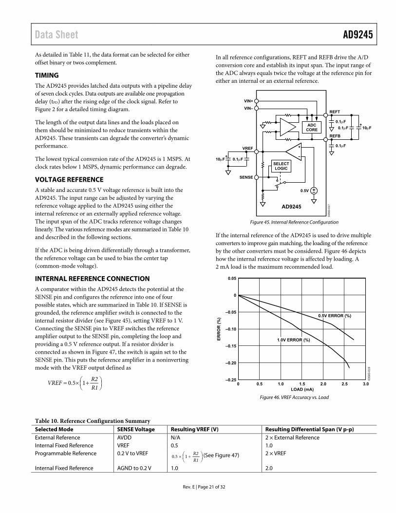
An internal differential reference buffer creates positive and negative reference voltages, REFT and REFB, that define the span of the ADC core. The output common mode of the reference buffer is set to midsupply, and the REFT and REFB voltages and span are defined as:
REFT = ½ (AVDD + VREF)
REFB = ½ (AVDD − VREF)
Span = 2 × (REFT − REFB) = 2 × VREF
The previous equations show that the REFT and REFB voltages are symmetrical about the midsupply voltage, and, by definition, the input span is twice the value of the VREF voltage.
The internal voltage reference can be pin strapped to fixed values of 0.5 V or 1.0 V, or adjusted within the same range as discussed in the Internal Reference Connection section. Maximum SNR performance is achieved with the AD9245 set to the largest input span of 2 V p-p. The relative SNR degradation is 3 dB when changing from 2 V p-p mode to 1 V p-p mode.

Data Sheet AD9245
Rev. E | Page 19 of 32
The SHA can be driven from a source that keeps the signal peaks within the allowable range for the selected reference voltage. The minimum and maximum common-mode input levels are defined as
2VREFVCMMIN =
( )2VREFAVDDVCMMAX
+=
The minimum common-mode input level allows the AD9245 to accommodate ground referenced inputs.
Although optimum performance is achieved with a differential input, a single-ended source can be applied to VIN+ or VIN–. In this configuration, one input accepts the signal, while the opposite input is set to midscale by connecting it to an appropriate reference. For example, a 2 V p-p signal can be applied to VIN+ while a 1 V reference is applied to VIN–. The AD9245 then accepts an input signal varying between 2 V and 0 V. In the single-ended configuration, distortion performance can degrade significantly as compared to the differential case. However, the effect is less noticeable at lower input frequencies.
Differential Input Configurations
As previously detailed, optimum performance is achieved while driving the AD9245 in a differential input configuration. For baseband applications, the AD8351 differential driver provides excellent performance and a flexible interface to the ADC. The output common-mode voltage of the AD8351 is easily set to AVDD/2, and the driver can be configured in a Sallen-Key filter topology to provide band limiting of the input signal.
0358
3-01
3
AD9245
VIN+
VIN–AGND
AVDD
2V p-p
33Ω
33Ω
20pFAD8351
1kΩ
1kΩ
0.1µF
1.2kΩ
25Ω
0.1mF25Ω
50Ω
Figure 40. Differential Input Configuration Using the AD8351
At input frequencies in the second Nyquist zone and above, the performance of most amplifiers is not adequate to achieve the true performance of the AD9245. This is especially true in IF undersampling applications where frequencies in the 70 MHz to 100 MHz range are being sampled. For these applications, differential transformer coupling is the recommended input configuration. The value of the shunt capacitor is dependent on the input frequency and source impedance and should be reduced or removed. An example is shown in Figure 41.
0358
3-01
4
AD9245
VIN+
VIN–
AVDD
AGND
33Ω
33Ω
20pF49.9Ω
1kΩ
1kΩ0.1µF
2V p-p
Figure 41. Differential Transformer-Coupled Configuration
The signal characteristics must be considered when selecting a transformer. Most RF transformers saturate at frequencies below a few MHz, and excessive signal power can also cause core saturation, which leads to distortion.
Single-Ended Input Configuration
A single-ended input can provide adequate performance in cost-sensitive applications. In this configuration, there is a degradation in SFDR and distortion performance due to the large input common-mode swing (see Figure 13). However, if the source impedances on each input are matched, there should be little effect on SNR performance. Figure 42 details a typical single-ended input configuration.
0358
3-01
5
AD9245
VIN+
VIN–
AVDD
AGND
2V p-p
33Ω
33Ω
20pF49.9Ω
1kΩ
1kΩ
0.33µF
10µF 0.1µF
1kΩ
1kΩ
+
Figure 42. Single-Ended Input Configuration
CLOCK INPUT CONSIDERATIONS Typical high speed ADCs use both clock edges to generate a variety of internal timing signals, and as a result can be sensitive to clock duty cycle. Commonly a 5% tolerance is required on the clock duty cycle to maintain dynamic performance characteristics. The AD9245-80 and AD9245-65 contain a clock duty cycle stabilizer (DCS) that retimes the nonsampling edge, providing an internal clock signal with a nominal 50% duty cycle. This allows a wide range of clock input duty cycles without affecting the performance of the AD9245. As shown in Figure 21, noise and distortion performance is nearly flat for a 30% to 70% duty cycle with the DCS on.
The duty cycle stabilizer uses a delay-locked loop (DLL) to create the nonsampling edge. As a result, any changes to the sampling frequency require approximately 100 clock cycles to allow the DLL to acquire and lock to the new rate.

AD9245 Data Sheet
Rev. E | Page 20 of 32
JITTER CONSIDERATIONS High speed, high resolution ADCs are sensitive to the quality of the clock input. The degradation in SNR at a given input frequency (fINPUT) due only to aperture jitter (tJ) can be calculated with the following equation:
SNR = −20log10[2π fINPUT × tj]
In the equation, the rms aperture jitter represents the root-mean square of all jitter sources, which include the clock input, analog input signal, and ADC aperture jitter specification. IF undersampling applications are particularly sensitive to jitter (see Figure 43).
The clock input should be treated as an analog signal in cases where aperture jitter can affect the dynamic range of the AD9245. Power supplies for clock drivers should be separated from the ADC output driver supplies to avoid modulating the clock signal with digital noise. Low jitter, crystal-controlled oscillators make the best clock sources. If the clock is generated from another type of source (by gating, dividing, or other methods), it should be retimed by the original clock at the last step.
INPUT FREQUENCY (MHz)
SN
R (
dB
c)
140
75
70
65
60
55
50
45
100010010
0358
3-04
1
0.2ps
MEASURED SNR
0.5ps
1.0ps
1.5ps
2.0ps
2.5ps
3.0ps
Figure 43. SNR vs. Input Frequency and Jitter
POWER DISSIPATION AND STANDBY MODE As shown in Figure 44, the power dissipated by the AD9245 is proportional to its sample rate. The digital power dissipation is determined primarily by the strength of the digital drivers and the load on each output bit. The maximum DRVDD current (IDRVDD) can be calculated as
NfCVI CLKLOADDRVDDDRVDD
where N is the number of output bits, 14 in the case of the AD9245. This maximum current occurs when every output bit switches on every clock cycle, that is, a full-scale square wave at the Nyquist frequency, fCLK/2. In practice, the DRVDD current is established by the average number of output bits switching,
which is determined by the sample rate and the characteristics of the analog input signal.
450
400
350
300
250
200
150
100
50
TO
TA
L P
OW
ER
(m
W)
0358
3-07
4
0 10 20 30 40 50 60 70 80
SAMPLE RATE (MSPS)
AD9245-80
AD9245-65
AD9245-40
AD9245-20
Figure 44. AD9245 Power vs. Sample Rate @ 2.5 MHz
Reducing the capacitive load presented to the output drivers can minimize digital power consumption. The data in Figure 44 was taken with the same operating conditions as those reported in the Typical Performance Characteristics section, and with a 5 pF load on each output driver.
By asserting the PDWN pin high, the AD9245 is placed in standby mode. In this state, the ADC typically dissipates 1 mW if the CLK and analog inputs are static. During standby, the output drivers are placed in a high impedance state. Reasserting the PDWN pin low returns the AD9245 to its normal operational mode.
Low power dissipation in standby mode is achieved by shutting down the reference, reference buffer, and biasing networks. The decoupling capacitors on REFT and REFB are discharged when entering standby mode and then must be recharged when returning to normal operation. As a result, the wake-up time is related to the time spent in standby mode, and shorter standby cycles result in proportionally shorter wake-up times. With the recommended 0.1 μF and 10 μF decoupling capacitors on REFT and REFB, it takes approximately 1 second to fully discharge the reference buffer decoupling capacitors and 7 ms to restore full operation.
DIGITAL OUTPUTS The AD9245 output drivers can be configured to interface with 2.5 V or 3.3 V logic families by matching DRVDD to the digital supply of the interfaced logic. The output drivers are sized to provide sufficient output current to drive a wide variety of logic families. However, large drive currents tend to cause current glitches on the supplies, which can affect converter performance. Applications requiring the ADC to drive large capacitive loads or large fanouts can require external buffers or latches.
Data Sheet AD9245
Rev. E | Page 21 of 32
As detailed in Table 11, the data format can be selected for either offset binary or twos complement.
TIMING The AD9245 provides latched data outputs with a pipeline delay of seven clock cycles. Data outputs are available one propagation delay (tPD) after the rising edge of the clock signal. Refer to Figure 2 for a detailed timing diagram.
The length of the output data lines and the loads placed on them should be minimized to reduce transients within the AD9245. These transients can degrade the converter’s dynamic performance.
The lowest typical conversion rate of the AD9245 is 1 MSPS. At clock rates below 1 MSPS, dynamic performance can degrade.
VOLTAGE REFERENCE A stable and accurate 0.5 V voltage reference is built into the AD9245. The input range can be adjusted by varying the reference voltage applied to the AD9245 using either the internal reference or an externally applied reference voltage. The input span of the ADC tracks reference voltage changes linearly. The various reference modes are summarized in Table 10 and described in the following sections.
If the ADC is being driven differentially through a transformer, the reference voltage can be used to bias the center tap (common-mode voltage).
INTERNAL REFERENCE CONNECTION A comparator within the AD9245 detects the potential at the SENSE pin and configures the reference into one of four possible states, which are summarized in Table 10. If SENSE is grounded, the reference amplifier switch is connected to the internal resistor divider (see Figure 45), setting VREF to 1 V. Connecting the SENSE pin to VREF switches the reference amplifier output to the SENSE pin, completing the loop and providing a 0.5 V reference output. If a resistor divider is connected as shown in Figure 47, the switch is again set to the SENSE pin. This puts the reference amplifier in a noninverting mode with the VREF output defined as
R1R2VREF 15.0
In all reference configurations, REFT and REFB drive the A/D conversion core and establish its input span. The input range of the ADC always equals twice the voltage at the reference pin for either an internal or an external reference.
0358
3-01
7
10F+
0.1F
VREF
SENSE
0.5V
AD9245
VIN–
VIN+
REFT
0.1F
0.1F 10F
0.1F
REFB
SELECTLOGIC
ADCCORE
+
Figure 45. Internal Reference Configuration
If the internal reference of the AD9245 is used to drive multiple converters to improve gain matching, the loading of the reference by the other converters must be considered. Figure 46 depicts how the internal reference voltage is affected by loading. A 2 mA load is the maximum recommended load.
LOAD (mA)
ER
RO
R (
%)
0.05
0 0.5 1.0 1.5 2.0 2.5 3.0
0358
3-01
9
0
–0.25
–0.20
–0.15
–0.10
–0.050.5V ERROR (%)
1.0V ERROR (%)
Figure 46. VREF Accuracy vs. Load
Table 10. Reference Configuration Summary Selected Mode SENSE Voltage Resulting VREF (V) Resulting Differential Span (V p-p) External Reference AVDD N/A 2 × External Reference Internal Fixed Reference VREF 0.5 1.0 Programmable Reference 0.2 V to VREF
R1R210.5 (See Figure 47) 2 × VREF
Internal Fixed Reference AGND to 0.2 V 1.0 2.0

AD9245 Data Sheet
Rev. E | Page 22 of 32
0358
3-01
8
10F+
0.1F
VREF
SENSE
R2
R1 0.5V
AD9245
VIN–
VIN+
REFT
0.1F
0.1F 10F
0.1F
REFB
SELECTLOGIC
ADCCORE
+
Figure 47. Programmable Reference Configuration
EXTERNAL REFERENCE OPERATION The use of an external reference can be necessary to enhance the gain accuracy of the ADC or improve thermal drift char-acteristics. When multiple ADCs track one another, a single reference (internal or external) can be necessary to reduce gain matching errors to an acceptable level. Figure 48 shows the typical drift characteristics of the internal reference in both 1.0 V and 0.5 V modes.
When the SENSE pin is tied to AVDD, the internal reference is disabled, allowing the use of an external reference. An internal reference buffer loads the external reference with an equivalent 7 kΩ load. The internal buffer still generates the positive and negative full-scale references, REFT and REFB, for the ADC core. The input span is always twice the value of the reference voltage; therefore, the external reference must be limited to a maximum of 1.0 V.
TEMPERATURE (°C)
VR
EF
ER
RO
R (
%)
–400
1.0
0.9
0.8
0.7
0.6
0.5
0.4
0.3
0.2
0.1
80706050403020100–10–20–30
0358
3-04
0
VREF = 0.5V
VREF = 1.0V
Figure 48. Typical VREF Drift
OPERATIONAL MODE SELECTION As discussed earlier, the AD9245 can output data in either offset binary or twos complement format. There is also a provision for enabling or disabling the clock DCS. The MODE pin is a multilevel input that controls the data format and DCS state. The input threshold values and corresponding mode selections are outlined in Table 11.
Table 11. Mode Selection MODE Voltage Data Format Duty Cycle Stabilizer AVDD Twos Complement Disabled 2/3 AVDD Twos Complement Enabled 1/3 AVDD Offset Binary Enabled AGND (Default) Offset Binary Disabled
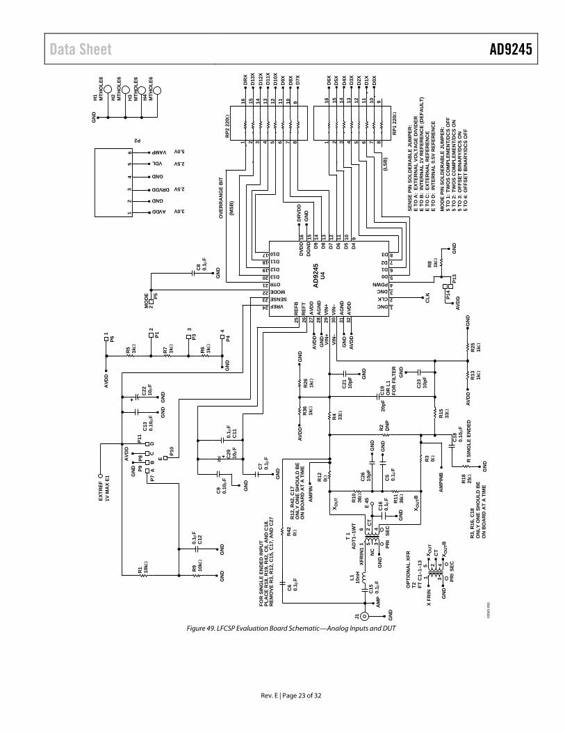
EVALUATION BOARD The AD9245 evaluation board provides the support circuitry required to operate the ADC in its various modes and configurations. Complete schematics and layout plots follow and demonstrate the proper routing and grounding techniques that should be applied at the system level.
It is critical that signal sources with very low phase noise (<1 ps rms jitter) be used to realize the ultimate performance of the converter. Proper filtering of the input signal, to remove harmonics and lower the integrated noise at the input, is also necessary to achieve the specified noise performance.
The AD9245 can be driven single-ended or differentially through a transformer. Separate power pins are provided to isolate the DUT from the support circuitry. Each input configuration can be selected by proper connection of various jumpers (refer to the schematics).
An alternative differential analog input path using an AD8351 op amp is included in the layout but is not populated in production. Designers interested in evaluating the op amp with the ADC should remove C15, R12, and R3 and populate the op amp circuit. The passive network between the AD8351 outputs and the AD9245 allows the user to optimize the frequency response of the op amp for the application.
Data Sheet AD9245
Rev. E | Page 23 of 32
0358
3-05
0
12
34
56
P13
P14
XFR
IN1
OPT
ION
AL
XFR
T2 FT C
1–1 –
13
NC
CT
1
T 1
AD
T1–1
WT
6 23
45
12
345
R S
ING
LE E
ND
EDR
1825
ΩR
3, R
16, C
18O
NLY
ON
E SH
OU
LD B
EO
N B
OA
RD
AT
A T
IME
EXTR
EF1V
MA
X E1
R1
10kΩ
R9
10k Ω
0.1 µ
FC
12
C9
0.10
µ FG
ND
GN
DG
ND
GN
D
GN
DA
VDD
C29
10µF
0.1µ
FC
11
C7
0.1µ
F
GN
D
GN
D
AVD
D
P7A
BC
D
P9P8
P11
P10
E
C13
0.10
µ FC
2210
µF
P6
P1 P3 P4
1
2 3 4
GN
D
GN
DC8
0.1µ
F
P52M
OD
E
25 26 27 28 29 30 31 32
2423222120191817
12345678
REF
BR
EFT
AVD
DA
GN
DVI
N+
AG
ND
AV D
D
VIN
–
AD
9245
U4
VREFSENSEMODE
D13OTR
D12D11D10
DVD
DD
GN
DD
9
D7D8
D6
D5
D4
16 15 14 13 12 11 10 9
DNCCLKDNC
D0PDWN
D1D2D3
(LSB
)
DRV
DD
GN
D
1 2 3 4 5 6 7 81 2 3 4 5 6 7 8
16 15 14 13 12 11 10 916 15 14 13 12 11 10 9
DR
XD
13X
D12
X
D10
XD
11X
D9X
D8X D7X
D6X
D5X
D4X
D2XD3X
D1X
D0X
(MSB
)
OVE
RR
AN
GE
BIT
AVDD
GND
DRVDD
VDL
VAMP
GND
P2
GN
DH
1M
THO
LE6
H2
MTH
OLE
6
H3
MTH
OLE
6
H4
MTH
OLE
6
3.0V
2.5V
2.5V
5.0V
RP2
220
Ω
RP1
220
Ω
SEN
SE P
IN S
OLD
ERA
BLE
JU
MPE
R:
E TO
A:
EXTE
RN
AL
VOLT
AG
E D
IVID
ERE
TO B
:IN
TER
NA
L 1V
REF
EREN
CE
(DEF
AU
LT)
E TO
C:
EXTE
RN
AL
REF
EREN
CE
E TO
D:
INTE
RN
AL
0.5V
REF
EREN
CE
MO
DE
PIN
SO
LDER
AB
LE J
UM
PER
:5
TO 1
: TW
OS
CO
MPL
EMEN
T/D
CS
OFF
5 TO
2:T
WO
S C
OM
PLEM
ENT/
DC
S O
N5
TO 3
: OFF
SET
BIN
AR
Y/D
CS
ON
5 TO
4: O
FFSE
T B
INA
RY/
DC
S O
FF
GN
D
R8
1kΩ
CLK
AVD
D
GN
DR
251k
ΩR
131k
Ω
A VD
D
R15
33Ω
GN
D
GN
D
C23
10pF
GN
D
C19
OR
L1
FOR
FIL
TER
GN
DA VD
D
R4
33ΩR36
1kΩ
R26
1kΩ
GN
D
AVD
D
A VD
D
GN
D
GN
D
VIN
+VI
N–
20pF
C21
10pF
R2
DN
P
R10
36Ω
R12
0 Ω
AM
PIN
X OU
T
GN
D X OU
TB
R3
0 Ω
R11
36Ω
C5
0.1 µ
F
C26
10pF
E 45
C16
0.1 µ
F
R42
0ΩC
6
FOR
SIN
GLE
EN
DED
INPU
TPL
AC
E R
18, R
19, R
42, C
6, A
ND
C18
.R
EMO
VE R
3, R
12, C
15, C
17, A
ND
C27 R
12, R
42, C
17O
NLY
ON
E SH
OU
LD B
EO
N B
OA
RD
AT
A T
IME
0.1µ
F
GN
D
GN
D
AM
P
AM
PIN
B
C15
0.1 µ
FL1 10nH
GN
DPR
ISE
C
PRI
SEC
GN
D
C18
0.10
µ F
X FR
IN
X OU
TBC
TX O
UT
J1
R5
1kΩ
R7
1kΩ
R6
1kΩ
Figure 49. LFCSP Evaluation Board Schematic—Analog Inputs and DUT
AD9245 Data Sheet
Rev. E | Page 24 of 32
0358
3-05
1
DR
XD
13X
GN
D
D2X D1X
GN
DD
0X
D11
XD
12X
DRV
DD
D10
XD
9XG
ND
D8X
D7X
D5XD6X
GN
DD
4XD
3XD
RVD
D
2CLK
2DB
2D7
GN
D2D
62D
5
1D2
1D1
1CLK
2D4
V CC
V CC
2D3
GN
D2D
22D
1
1D7
1D6
1D5
1D8
GN
D
1D4
1D3
GN
D
2OE
2QB
2Q7
2Q6
2Q5
1Q2
1Q1
1OE
2Q4
2Q3
GN
D
GN
D
2Q2
2Q1
1Q8
1Q7
1Q6
1Q5
GN
D
V CC
V CC
1Q4
1Q3
GN
D
25 26 27 28 29 30 31 32 33 34 35 36 37 38 39 40 41 42 43 44 45 46 47 48
24 23 22 21 20 19 18 17 16 15 14 13 12 11 10 9 8 7 6 5 4 3 2 1IN
OU
T
CLK
AT/D
AC
1U1
74LV
TH16
2374
CLK
LAT/
DA
C
GN
D
GN
D
DRV
DD
GN
D
GN
D
DRV
DD
GN
D
GN
D
DRY
MSB LS
B
2 4 6 8 10 12 14 16 18 20 22 24 26 28 30 32 34 36 38 40
2 4 6 8 10 12 14 16 18 20 22 24 26 28 30 32 34 36 38 40
1 3 5 7 9 11 13 15 17 19 21 23 25 27 29 31 33 35 37 39
1 3 5 7 9 11 13 15 17 19 21 23 25 27 29 31 33 35 37 39
GN
DD
RG
ND
MSB
DRY G
ND
AM
PIN
AM
PIN
B
GN
D
VAM
P
GN
D
GN
D
GN
D
GN
D
VAM
P
GN
D
VAM
P
GN
D
GN
D
P12
C27
0.1µ
F
C45
0.1µ
F
C28
0.1µ
F
C35
0.10
µ F
C24
10µF
C17
0.1µ
F
R16
0 Ω
R39
1kΩ
R14
25Ω
R40
10kΩ
PWD
N 1
RG
P1 2
INH
I 3
INLO
4
RPG
2 5
R41
10kΩ
R35
25Ω
R33
25Ω
R34
1.2k
Ω
R19
50Ω
AM
P IN
AM
P
R17
0Ω
R38
1kΩ
U3
AD
8351
POW
ER D
OW
NU
SE R
40 O
R R
41C
440.
1µF
GN
D
GN
DC
OM
M678910
OPL
O
OPH
IVP
OS
VOC
M
TO U
SE A
MPL
IFIE
RPL
AC
E A
LL C
OM
PON
ENTS
SHO
WN
HER
E (R
IGH
T)EX
CEP
T R
40 O
R R
41.
REM
OVE
R12
, R3,
R18
, R42
,C
6, C
15, A
ND
C18
.
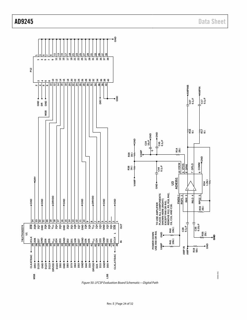
Figure 50. LFCSP Evaluation Board Schematic—Digital Path

Data Sheet AD9245
Rev. E | Page 25 of 32
0358
3-05
2
C10
10µF
C4
10µF
C3
10µF
C25
10µF
C32
0.00
1µF
C33
0.1µ
FC
140.
001 µ
F
VDL
DRV
DD
AVD
D
GN
DG
ND
AV D
D
DU
T B
YPA
SSIN
G
CLO
CK
TIM
ING
AD
JUST
MEN
TS
FOR
A B
UFF
ERED
EN
CO
DE
USE
R28
FOR
A D
IREC
T EN
CO
DE
USE
R27
AN
ALO
G B
YPA
SSIN
GD
IGIT
AL
BYP
ASS
ING
LATC
H B
YPA
SSIN
G
GN
D
DRV
DD
C41
0.1µ
FC
210
µ FC
300.
001 µ
FC
310.
1µF
C46
10µF
C34
0.1µ
FC
360.
1µF
C38
0.00
1µF
C1
0.1 µ
FC
470.
1µF
C48
0.00
1 µF
C49
0.00
1µF
C20
10µF
C37
0.1µ
FC
400.
001µ
F
GN
D
GN
D
VAM
P
VDL
C39
0.00
1µF
ENC
X
CLK
ENC
ENC
OD
E
R27
0 ΩR
321k
ΩR
23 0 ΩR
37 0 Ω
R22
0 Ω
R28
0 Ω
E50
E51
ENC
VDL VD
LVDLE5
2E5
3
E31
E35
E43
E44G
ND
GN
D
GN
D
PWR
GN
DC
LKLA
T/D
AC
VDL
GN
D
VDL
GN
D
C43
0.1 µ
FR
311k
ΩR
201k
Ω
R21
1kΩ
R24
1kΩ
R30
1kΩ
R29
50Ω
GN
D
J2
GN
D
VDL
GN
D
11Y
U54Y2Y 3Y
2 4 5 9 10
3 6 7 8 11 1412 13
74VC
X86
ENC
X
1B1A 2B2A 3B3A 4B4A
DR
SCH
EMA
TIC
SH
OW
S TW
O G
ATE
DEL
AY
SETU
P.FO
R O
NE
DEL
AY,
REM
OVE
R22
AN
D R
37 A
ND
ATT
AC
H R
x (R
x =
0Ω).
Rx
DN
P
LATC
H B
YPA
SSIN
G
Figure 51. LFCSP Evaluation Board Schematic—Clock Input
AD9245 Data Sheet
Rev. E | Page 26 of 32
0358
3-05
3
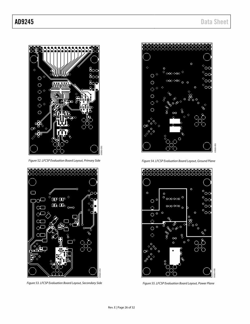
Figure 52. LFCSP Evaluation Board Layout, Primary Side
0358
3-05
4
Figure 53. LFCSP Evaluation Board Layout, Secondary Side
0358
3-05
5
Figure 54. LFCSP Evaluation Board Layout, Ground Plane
0358
3-05
6
Figure 55. LFCSP Evaluation Board Layout, Power Plane
Data Sheet AD9245
Rev. E | Page 27 of 32
0358
3-05
7
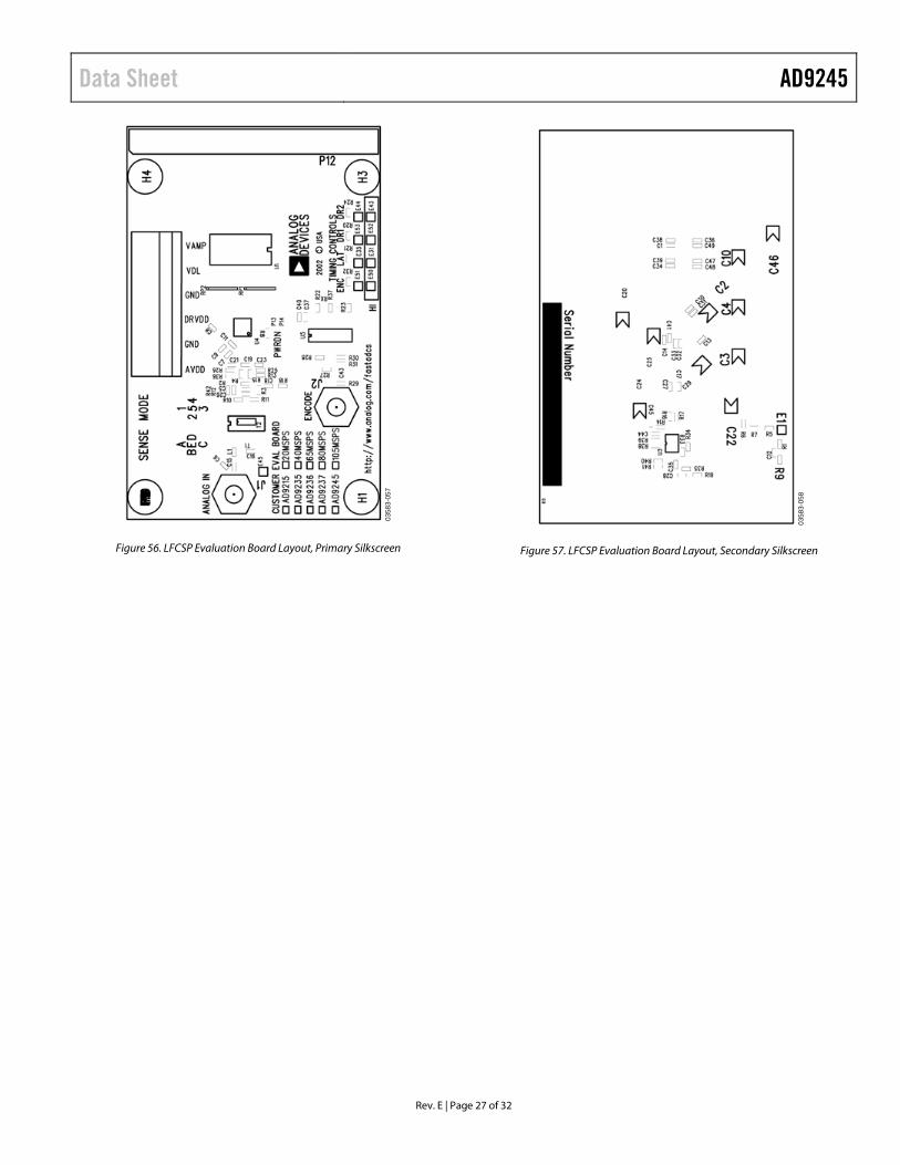
Figure 56. LFCSP Evaluation Board Layout, Primary Silkscreen
0358
3-05
8
Figure 57. LFCSP Evaluation Board Layout, Secondary Silkscreen
AD9245 Data Sheet
Rev. E | Page 28 of 32
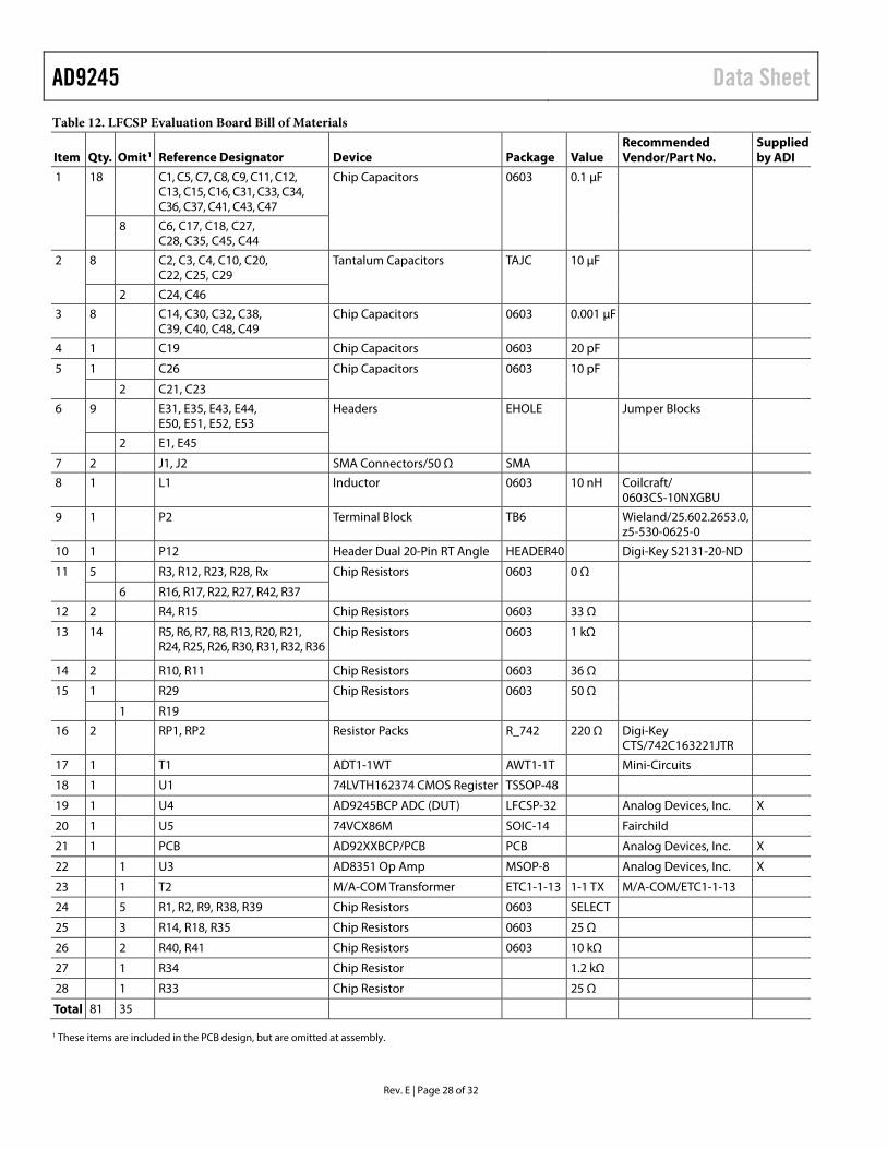
Table 12. LFCSP Evaluation Board Bill of Materials
Item Qty. Omit1 Reference Designator Device Package Value Recommended Vendor/Part No.
Supplied by ADI
1 18 C1, C5, C7, C8, C9, C11, C12, C13, C15, C16, C31, C33, C34, C36, C37, C41, C43, C47
Chip Capacitors 0603 0.1 µF
8 C6, C17, C18, C27, C28, C35, C45, C44
2 8 C2, C3, C4, C10, C20, C22, C25, C29
Tantalum Capacitors TAJC 10 µF
2 C24, C46
3 8 C14, C30, C32, C38, C39, C40, C48, C49
Chip Capacitors 0603 0.001 µF
4 1 C19 Chip Capacitors 0603 20 pF
5 1 C26 Chip Capacitors 0603 10 pF
2 C21, C23
6 9 E31, E35, E43, E44, E50, E51, E52, E53
Headers EHOLE Jumper Blocks
2 E1, E45
7 2 J1, J2 SMA Connectors/50 Ω SMA
8 1 L1 Inductor 0603 10 nH Coilcraft/ 0603CS-10NXGBU
9 1 P2 Terminal Block TB6 Wieland/25.602.2653.0, z5-530-0625-0
10 1 P12 Header Dual 20-Pin RT Angle HEADER40 Digi-Key S2131-20-ND
11 5 R3, R12, R23, R28, Rx Chip Resistors 0603 0 Ω
6 R16, R17, R22, R27, R42, R37
12 2 R4, R15 Chip Resistors 0603 33 Ω
13 14 R5, R6, R7, R8, R13, R20, R21, R24, R25, R26, R30, R31, R32, R36
Chip Resistors 0603 1 kΩ
14 2 R10, R11 Chip Resistors 0603 36 Ω
15 1 R29 Chip Resistors 0603 50 Ω
1 R19
16 2 RP1, RP2 Resistor Packs R_742 220 Ω Digi-Key CTS/742C163221JTR
17 1 T1 ADT1-1WT AWT1-1T Mini-Circuits
18 1 U1 74LVTH162374 CMOS Register TSSOP-48
19 1 U4 AD9245BCP ADC (DUT) LFCSP-32 Analog Devices, Inc. X
20 1 U5 74VCX86M SOIC-14 Fairchild
21 1 PCB AD92XXBCP/PCB PCB Analog Devices, Inc. X
22 1 U3 AD8351 Op Amp MSOP-8 Analog Devices, Inc. X
23 1 T2 M/A-COM Transformer ETC1-1-13 1-1 TX M/A-COM/ETC1-1-13
24 5 R1, R2, R9, R38, R39 Chip Resistors 0603 SELECT
25 3 R14, R18, R35 Chip Resistors 0603 25 Ω
26 2 R40, R41 Chip Resistors 0603 10 kΩ
27 1 R34 Chip Resistor 1.2 kΩ
28 1 R33 Chip Resistor 25 Ω
Total 81 35 1 These items are included in the PCB design, but are omitted at assembly.

Data Sheet AD9245
Rev. E | Page 29 of 32
OUTLINE DIMENSIONS
COMPLIANT TO JEDEC STANDARDS MO-220-WHHD. 1124
08-A
10.50BSC
BOTTOM VIEWTOP VIEW
PIN 1INDICATOR
32
916
17
24
25
8
EXPOSEDPAD
PIN 1INDICATOR
3.253.10 SQ2.95
SEATINGPLANE
0.05 MAX0.02 NOM
0.20 REF
COPLANARITY0.08
0.300.250.18
5.105.00 SQ4.90
0.800.750.70
FOR PROPER CONNECTION OFTHE EXPOSED PAD, REFER TOTHE PIN CONFIGURATION ANDFUNCTION DESCRIPTIONSSECTION OF THIS DATA SHEET.
0.500.400.30
0.25 MIN
Figure 58. 32-Lead Frame Chip Scale Package [LFCSP_WQ]
5 mm × 5 mm Body, Very Very Thin Quad (CP-32-7)
Dimensions shown in millimeters
ORDERING GUIDE Model1 Temperature Range Package Description Package Option AD9245BCPZ-80 –40°C to +85°C 32-Lead Lead Frame Chip Scale Package (LFCSP_WQ) CP-32-7 AD9245BCPZRL7-80 –40°C to +85°C 32-Lead Lead Frame Chip Scale Package (LFCSP_WQ) CP-32-7 AD9245BCPZ-65 –40°C to +85°C 32-Lead Lead Frame Chip Scale Package (LFCSP_WQ) CP-32-7 AD9245BCPZRL7-65 –40°C to +85°C 32-Lead Lead Frame Chip Scale Package (LFCSP_WQ) CP-32-7 AD9245BCPZ-40 –40°C to +85°C 32-Lead Lead Frame Chip Scale Package (LFCSP_WQ) CP-32-7 AD9245BCPZRL7-40 –40°C to +85°C 32-Lead Lead Frame Chip Scale Package (LFCSP_WQ) CP-32-7 AD9245BCPZ-20 –40°C to +85°C 32-Lead Lead Frame Chip Scale Package (LFCSP_WQ) CP-32-7 AD9245BCPZRL7-20 –40°C to +85°C 32-Lead Lead Frame Chip Scale Package (LFCSP_WQ) CP-32-7 1 Z = RoHS-Compliant Part.

AD9245 Data Sheet
Rev. E | Page 30 of 32
NOTES

Data Sheet AD9245
Rev. E | Page 31 of 32
NOTES

AD9245 Data Sheet
Rev. E | Page 32 of 32
NOTES
© 2013 Analog Devices, Inc. All rights reserved. Trademarks and registered trademarks are the property of their respective owners. D03583-0-5/13(E)