Embed Size (px)
Citation preview

11
IntelLabsJuly 5, 2005
Microprocessor and DSP Microprocessor and DSP Technologies for the Technologies for the
Nanoscale EraNanoscale Era
Microprocessor and DSP Microprocessor and DSP Technologies for the Technologies for the
Nanoscale EraNanoscale EraSeminar 1Seminar 1
Ram Kumar KrishnamurthyRam Kumar KrishnamurthyMicroprocessor Research LabsMicroprocessor Research LabsIntel Corporation, Hillsboro, ORIntel Corporation, Hillsboro, [email protected]@intel.com
Seminar 1Seminar 1Ram Kumar KrishnamurthyRam Kumar Krishnamurthy
Microprocessor Research LabsMicroprocessor Research LabsIntel Corporation, Hillsboro, ORIntel Corporation, Hillsboro, [email protected]@intel.com

IntelLabs22
• Established 1996Established 1996
• Belongs under Microprocessor Technology LabsBelongs under Microprocessor Technology Labs
• Located in Hillsboro, Oregon, USA (primary) and Located in Hillsboro, Oregon, USA (primary) and
Bangalore, IndiaBangalore, India
• 75 researchers75 researchers
• Charter:Charter:
• High-performance & low-power digital circuitsHigh-performance & low-power digital circuits
• Off-chip I/O signaling circuitsOff-chip I/O signaling circuits
• Power delivery circuitsPower delivery circuits
• >50 patents, >25 papers per year>50 patents, >25 papers per year
About Circuits Research LabAbout Circuits Research Lab

33
0.01
0.1
1
10
100
1000
10000
100000
1000000
1970 1980 1990 2000 2010
MIP
S
Pentium® Pro Architecture
Pentium® 4 Architecture
Pentium® Architecture
486386
2868086
Strong demand for > 1 TIPS performance beyond this decadeStrong demand for > 1 TIPS performance beyond this decadeHow do you get there?How do you get there?
Strong demand for > 1 TIPS performance beyond this decadeStrong demand for > 1 TIPS performance beyond this decadeHow do you get there?How do you get there?
Motivation: Higher performance at Motivation: Higher performance at lower power and costlower power and cost

44
Our Research Agenda OutlookOur Research Agenda Outlook
20042004 20062006 20082008 20102010 20122012 20142014 20162016 20182018
Technology Node Technology Node (nm)(nm)
9090 6565 4545 3232 2222 1616 1111 88
Integration Integration Capacity (BT)Capacity (BT)
0.50.5 11 22 44 88 1616 3232 6464
Delay = CV/I Delay = CV/I scalingscaling
0.70.7 ~0.7~0.7 >0.7>0.7 Delay scaling will slow downDelay scaling will slow down
Energy/Logic Op Energy/Logic Op scalingscaling
>0.35>0.35 >0.5>0.5 >0.5>0.5 Energy scaling will slow downEnergy scaling will slow down
Bulk Planar CMOSBulk Planar CMOS High Probability Low ProbabilityHigh Probability Low ProbabilityAlternate, 3G etcAlternate, 3G etc Low Probability High ProbabilityLow Probability High ProbabilityVariabilityVariability Medium High Very HighMedium High Very HighILD (K)ILD (K) ~3~3 <3<3 Reduce slowly towards 2-2.5Reduce slowly towards 2-2.5RC DelayRC Delay 11 11 11 11 11 11 11 11
Metal LayersMetal Layers 6-76-7 7-87-8 8-98-9 0.5 to 1 layer per generation0.5 to 1 layer per generation
Internal UniversityFCRP(MARCO)

55
Intel’s Research FocusIntel’s Research FocusTechnology Leadership
Complete solution stack
0.01
0.1
1
1990 2000 2010
10
100
1000
nm
Gate Length
Industry
Intel
Technology Arch & Design Platforms Software

66
Architectures & DesignsArchitectures & DesignsBack End Back End
ServerServerServerServer DesktopDesktop MobileMobile HandheldHandheld
FamilyFamily Itanium®Itanium® Itanium ®Itanium ®
Xeon ®Xeon ®
Pentium ®Pentium ®
CeleronCeleron
Centrino ®Centrino ®
Pentium ®Pentium ®
Xscale ®Xscale ®
ArchitectureArchitecture IA64, VLIWIA64, VLIW IA64/ IA32IA64/ IA32 IA32IA32 IA32IA32 ARMARM
WordWord 64 bit64 bit 64 bit Itanium64 bit Itanium
32 bit Xeon32 bit Xeon
32 bit32 bit 32 bit32 bit 32 bit32 bit
Address Address SpaceSpace
HugeHuge Huge/4 GBHuge/4 GB 4 GB4 GB 4 GB4 GB 4 GB4 GB
CacheCache 6 MB6 MB 6 MB, 2 MB6 MB, 2 MB 1 MB1 MB 1 MB1 MB 512 KB512 KB
PerformancePerformance HighHigh HighHigh HighHigh MediumMedium LowLow
PowerPower ~130W~130W ~100 W~100 W < 100 W< 100 W ~25 W~25 W < 1W< 1W
Power MetricPower Metric Watts/sq ftWatts/sq ft
Watts/cu ftWatts/cu ft
WattsWatts Watt-hoursWatt-hours
Battery LifeBattery Life
CostCost HighHigh HighHigh MedMed MedMed LowLow
Our research agenda addresses all these platformsOur research agenda addresses all these platformsOur research agenda addresses all these platformsOur research agenda addresses all these platforms

77
Is Transistor a Good Switch?Is Transistor a Good Switch?
On
I = ∞
I = 0
Off
I = 0
I = 0
I ≠ 0
I = 1ma/u
I ≠ 0
I ≠ 0Sub-threshold Leakage

88
Sub-threshold LeakageSub-threshold Leakage
Transistors will not be Transistors will not be switchesswitches, but , but
dimmersdimmers
Transistors will not be Transistors will not be switchesswitches, but , but
dimmersdimmers
Ids(log)
Vgs
Vt
ExponentialIncrease in Ioff
MOS Transistor Characteristics
1
10
100
1000
10000
30 50 70 90 110 130
Temp (C)
Ioff
(n
a/u
)
0.25
90
45
0.1
1
10
100
1000
0.25u 0.18u 0.13u 90nm 65nm 45nm
Technology
SD
Lea
kag
e (W
atts
)
2X Tr Growth1.5X Tr Growth

99
Leakage PowerLeakage Power
0%
10%
20%
30%
40%
50%
1.5 1 0.7 0.5 0.35 0.25 0.18 0.13 0.09 0.07 0.05
Technology (m)
Lea
kag
e P
ow
er(%
of
To
tal)
Must stopat 50%
Leakage power limits Vt scalingLeakage power limits Vt scalingLeakage power limits Vt scalingLeakage power limits Vt scaling
A. Grove, IEDM 2002

1010
M21 M2j M2K
Pk0Clock
M11M1j M1K
I Leak
Dyn_out
INV_out
High Leakage High Leakage Impacts Functionality Impacts Functionality
Sub-65nm Dynamic Circuit Active Leakage Tolerance:Sub-65nm Dynamic Circuit Active Leakage Tolerance: Cache, RF, Arrays, Bitlines most affectedCache, RF, Arrays, Bitlines most affected Keeper sizes > 50% of pulldown strengthKeeper sizes > 50% of pulldown strength High contention High contention degraded performance degraded performance Slow keeper shutoff Slow keeper shutoff high short-circuit power high short-circuit power
1X 3X 5X 10X 20X
Subthreshold + gate leakage
0
0.4
0.8
1.2
1.6Sub-70nm
Kee
per
/ p
ulld
ow
n r
atio
M. Anders, R. Krishnamurthy et al, 2001 Symp. VLSI CircuitsM. Anders, R. Krishnamurthy et al, 2001 Symp. VLSI Circuits

1111
Power Will be the LimiterPower Will be the Limiter
0.001
0.01
0.1
1
10
100
1000
1970 1980 1990 2000 2010 2020
MillionTransistors
1 BillionTransistors
8080
8086
386 Pentium® proc
Pentium® 4 proc
0.1
1
10
100
1000
10000
100000
1970 1980 1990 2000 2010 2020
MHz
15-30 GHz
8080
8086
386 Pentium® proc
Pentium® 4 proc
0.01
0.1
1
10
100
1000
10000
100000
1000000
1970 1980 1990 2000 2010 2020
MIPS
1 TIPS
8080
8086
386 Pentium® proc
Pentium® 4 proc
0.1
1
10
100
1000
1970 1980 1990 2000 2010 2020
Power(Watts)
1000's ofWatts?
8080
8086386
Pentium® proc
Pentium® 4 proc
1B transistor integration capacity 1B transistor integration capacity willwill exist exist
Applications will demand TIPS performanceApplications will demand TIPS performance But the Power…But the Power…
Challenge: Highest performance in the power envelope Challenge: Highest performance in the power envelope Challenge: Highest performance in the power envelope Challenge: Highest performance in the power envelope

1212
Power TrendPower Trend
1
10
100
1985 1990 1995 2000
386386
Pentium® processorPentium® processor
Pentium® II processorPentium® II processor
Pentium® 4 processorPentium® 4 processor
Cooling Capacity Of Conventional SystemCooling Capacity Of Conventional System
C scales by 30% per generation…C scales by 30% per generation………but Vcc scales by 10-15% only!but Vcc scales by 10-15% only!
Must maintain or reduce power in futureMust maintain or reduce power in future
C scales by 30% per generation…C scales by 30% per generation………but Vcc scales by 10-15% only!but Vcc scales by 10-15% only!
Must maintain or reduce power in futureMust maintain or reduce power in future
486486
““Business As Usual”Business As Usual” is Not an Option is Not an Option
““Business As Usual”Business As Usual” is Not an Option is Not an Option
Po
wer
(W
)P
ow
er (
W)

1313
Gate Oxide is Near LimitGate Oxide is Near Limit
Poly Si Gate Electrode
Si Substrate
1.5 nm Gate Oxide
70 nm
Si3N4
CoSi2130nm Transistor
Intel’s High K leadershipIntel’s High K leadership is crucial for the is crucial for the
industryindustry
Intel’s High K leadershipIntel’s High K leadership is crucial for the is crucial for the
industryindustry
1.E-031.E-021.E-011.E+001.E+011.E+021.E+031.E+041.E+051.E+06
0.25u 0.18u 0.13u 90nm 65nm 45nm
Technology
Gat
e Le
akag
e (W
atts
) 1.5X2X
During Burn-in1.4X Vdd

1414
Power Density Will Get Even WorsePower Density Will Get Even Worse
Need to Keep the Junctions CoolNeed to Keep the Junctions Cool• Performance (Higher Frequency)Performance (Higher Frequency)• Lower leakage (Exponential) Lower leakage (Exponential) • Better reliability (Exponential)Better reliability (Exponential)
400440048008800880808080
80858085
80868086
286286 386386486486
PentiumPentium®® processorsprocessors
11
1010
100100
1,0001,000
10,00010,000
’’7070 ’’8080 ’’9090 ’’0000 ’’1010
Power DensityPower Density(W/cm2)(W/cm2)
Pat Gelsinger, ISSCC 2001

1515
Active Power ReductionActive Power Reduction
Slow Fast Slow
Lo
w S
up
ply
V
olt
age
Hig
h S
up
ply
V
olt
age
Logic BlockFreq = 1Vdd = 1Throughput = 1Power = 1Area = 1 Pwr Den = 1
Vdd
Logic Block
Freq = 0.5Vdd = 0.5Throughput = 1Power = 0.25Area = 2Pwr Den = 0.125
Vdd/2
Logic Block
Multiple Supply Voltages
Replicated Designs
Need high-speed multi-supply level converter techniquesNeed high-speed multi-supply level converter techniquesNeed high-speed multi-supply level converter techniquesNeed high-speed multi-supply level converter techniques

1616
Leakage ControlLeakage ControlStack EffectBody Bias Sleep Transistor
VddVbp
Vbn-Ve
+Ve
Equal Loading Logic Block
2-10X reduction 2-1000X reduction
Need low leakage and leakage tolerant techniquesNeed low leakage and leakage tolerant techniquesNeed low leakage and leakage tolerant techniquesNeed low leakage and leakage tolerant techniques2-200X reduction

1717
Dual Vt Design for Active Leakage ReductionDual Vt Design for Active Leakage Reduction
Logic path between latch boundaries
DelayNu
mb
er
of
pa
ths
DelayNu
mb
er
of
pa
ths
DelayNu
mb
er
of
pa
ths
Technology provides two Vt
High Vt with nominal Ioff (lower performance)
Low Vt with ~10X higher loff (higher performance)
Employing high Vt everywhere yields lowerperformance, and lower leakage (1X)
Employing low Vt everywhere yields higherperformance, but higher leakage (10X)
Selective usage of low and high Vt yields higher performance, yet low leakage between 1X, and <<10X
High Vt
Low Vt
Dual VtDual Vt

1818
Chip Multi-ProcessingChip Multi-Processing
1
1.5
2
2.5
3
3.5
1 2 3 4
Die Area, PowerR
ela
tive
Pe
rfo
rma
nce
CMP
ST
C1 C2
C3 C4
Cache
• Multi-core, each core Multi-threaded• Shared cache and front side bus• Each core has different Vdd & Freq• Core hopping to spread hot spots• Lower junction temperature

1919
Memory LatencyMemory Latency
MemoryCPU Cache
Small~few Clocks Large
50-100ns1
10
100
1000
100 1000 10000
Freq (MHz)M
em
ory
La
ten
cy
(C
loc
ks
)Assume: 50ns Memory latency
Cache miss hurts performanceCache miss hurts performanceWorse at higher frequencyWorse at higher frequency
Need power efficient high-speed I/O techniquesNeed power efficient high-speed I/O techniques
Cache miss hurts performanceCache miss hurts performanceWorse at higher frequencyWorse at higher frequency
Need power efficient high-speed I/O techniquesNeed power efficient high-speed I/O techniques

2020
Increase on-die MemoryIncrease on-die Memory
Pentium ® 4
Pentium III & 4Pentium III
Pentium II
Pentium Pro
Pentium
0%
20%
40%
60%
80%
100%
m m m m m m m
Cache % offull chiparea ?
Large on die memory provides:
1. Increased Data Bandwidth & Reduced Latency
2. Hence, higher performance for much lower power
1
10
100
m m m m
Po
we
r D
en
sit
y (
Wa
tts
/cm
2 )
Logic
Memory

2121
Special Purpose Hardware AccelerationSpecial Purpose Hardware Acceleration
TC
B ExecCore
PLL
OOO
ROMC
AM
1
TC
B ExecCore
PLL
ROB
ROMC
LB
Inputseq
Sendbuffer
2.23 mm X 3.54 mm, 260K transistors
Opportunities for acceleration:Network processing enginesMPEG Encode/Decode enginesSpeech enginesWireless communication/baseband
1.E+02
1.E+03
1.E+04
1.E+05
1.E+06
1995 2000 2005 2010 2015
MIP
S
GP MIPS@75W
TOE MIPS@~2W
Special purpose HW—Best MIPS/WattSpecial purpose HW—Best MIPS/WattSpecial purpose HW—Best MIPS/WattSpecial purpose HW—Best MIPS/Watt
TCP Offload EngineTCP Offload Engine

2222
ALUs: performance and peak-current limitersHigh activity thermal hotspotsGoal: high-performance energy-efficient design
Energy-efficient Data-path Circuits Energy-efficient Data-path Circuits
Execution core
Cache
Processor thermal
map
Integer and FP ALUs and
MACs
Temp(oC)

2323
130nm 9GHz 32-bit Integer ALU (ISSCC’02)130nm 9GHz 32-bit Integer ALU (ISSCC’02)
0.0
1.0
2.0
3.0
4.0
5.0
6.0
7.0
8.0
9.0
0.8 0.9 1.0 1.1 1.2 1.3 1.4 1.5Supply Voltage (V)
F max
(G
Hz)
0
50
100
150
200
250
300
350
400
450
0.8 0.9 1.0 1.1 1.2 1.3 1.4 1.5
Supply Voltage (V)
Po
wer
(m
W)
0
10
20
30
40
50
60
70
80
90
100
Lea
kag
e P
ow
er (
mW
)
Design target:6.5GHz at 120mWDie Size 1.61 x 1.44 mm
Process 130nm CMOS Interconnect 1 poly, 6 metal Transistors 160K Maximum VCC 1.5 V
RF
Input FIFO
Scan Ctl
ALU
Output FIFO
Clock
Misc
BB Ctl
M. Anders, R. Krishnamurthy et al,M. Anders, R. Krishnamurthy et al,Intl. Solid-state Circuits Conf. 2002 &Intl. Solid-state Circuits Conf. 2002 &
IEEE Journal of Solid-state Circuits 11/02IEEE Journal of Solid-state Circuits 11/02
32-bit integer exec core32-bit integer exec core32-bit integer exec core32-bit integer exec core

2424
Process Process 90nm Dual-Vt CMOS, 7 90nm Dual-Vt CMOS, 7 MetalMetal
Die areaDie area 0.474mm0.474mm22
64-bit ALU layout area64-bit ALU layout area 0.073mm0.073mm22
Total transistor countTotal transistor count 61006100
64-bit ALU average switching power (64-bit ALU average switching power (=0.3)=0.3) 89mW at 4GHz, 1.3V, 2589mW at 4GHz, 1.3V, 25ooCC
64-bit ALU active leakage power64-bit ALU active leakage power 9.6mW at 1.3V, 259.6mW at 1.3V, 25ooCC
64-bit ALU maximum frequency64-bit ALU maximum frequency 7GHz at 2.1V, 25C7GHz at 2.1V, 25C
32-bit ALU average switching power (32-bit ALU average switching power (=0.3)=0.3) 71mW at 7GHz, 1.3V, 2571mW at 7GHz, 1.3V, 25ooCC
32-bit ALU active leakage power32-bit ALU active leakage power 4.4mW at 1.3V, 254.4mW at 1.3V, 25ooCC
Lo
we
r-o
rder
3
2-b
it A
LU
Up
pe
r-o
rder
3
2-b
it A
LU
I/O CircuitsClock Generator and Drivers
90nm 7GHz 64-bit Integer ALU (ISSCC’04)90nm 7GHz 64-bit Integer ALU (ISSCC’04)
• 7GHz single-cycle 64-bit integer ALU (measured in 90nm CMOS) • Simultaneous 9GHz single-cycle 32-bit integer ALU mode• Fastest reported single-cycle 64-bit integer ALU performance
• 7GHz single-cycle 64-bit integer ALU (measured in 90nm CMOS) • Simultaneous 9GHz single-cycle 32-bit integer ALU mode• Fastest reported single-cycle 64-bit integer ALU performance
64-bit ALU die microphotograph and measured performance summary 64-bit ALU die microphotograph and measured performance summary
S. Mathew, R. Krishnamurthy et al,S. Mathew, R. Krishnamurthy et al,Intl. Solid-state Circuits Conf. 2004 &Intl. Solid-state Circuits Conf. 2004 &
IEEE Journal of Solid-state Circuits 01/05IEEE Journal of Solid-state Circuits 01/05

2525
90nm 1GHz 9mW 16*16b Multiplier (ISSCC’05)90nm 1GHz 9mW 16*16b Multiplier (ISSCC’05)
• 1GHz single-cycle 16*16-bit DSP multiplier (measured in 90nm CMOS) • Reconfigurable PLA control engine• 9pJ/Op or 110GOPS/Watt• Highest reported GOPS/Watt for single-cycle 16-bit multiply
• 1GHz single-cycle 16*16-bit DSP multiplier (measured in 90nm CMOS) • Reconfigurable PLA control engine• 9pJ/Op or 110GOPS/Watt• Highest reported GOPS/Watt for single-cycle 16-bit multiply
S. Hsu, R. Krishnamurthy et al,S. Hsu, R. Krishnamurthy et al,Intl. Solid-state Circuits Conf. 2005Intl. Solid-state Circuits Conf. 2005
Clock Generator and Drivers R
-PL
A
Reg
iste
rs
16x16b Multiplier I/O Circuits
Process Process 90nm Dual-V90nm Dual-Vtt CMOS CMOS
Die areaDie area 0.474mm0.474mm22
16b Multiplier and PLA layout area16b Multiplier and PLA layout area 0.03mm0.03mm22
16b Multiplier worst-case power16b Multiplier worst-case power 9mW at 1GHz, 1.3V, 509mW at 1GHz, 1.3V, 50ooC (nominal)C (nominal)
16b Multiplier active leakage power16b Multiplier active leakage power 540μW at 1.3V, 50540μW at 1.3V, 50ooC (nominal)C (nominal)
16b Multiplier peak performance16b Multiplier peak performance 1.5GHz, 32mW at 1.95V, 501.5GHz, 32mW at 1.95V, 50ooCC
16b Multiplier low-voltage mode performance16b Multiplier low-voltage mode performance 50MHz, 79μW at 0.57V, 5050MHz, 79μW at 0.57V, 50ooCC
Reconfigurable PLA peak performanceReconfigurable PLA peak performance 2.3GHz, 4.2mW at 1.3V, 50°C2.3GHz, 4.2mW at 1.3V, 50°C
Reconfigurable PLA worst-case powerReconfigurable PLA worst-case power 2mW at 1GHz, 1.3V, 502mW at 1GHz, 1.3V, 50ooC (nominal)C (nominal)
Stand-by mode powerStand-by mode power 75μW (7X reduction vs. active leakage)75μW (7X reduction vs. active leakage)
16*16-bit Multiplier die microphotograph and measured performance summary 16*16-bit Multiplier die microphotograph and measured performance summary

2626
32-bit ALU architecture32-bit ALU architecture
Multiple ALUs clustered together in the execution core High power density
Multiple ALUs clustered together in the execution core High power density
Loopback bus
Adder coreAdder coreSum
2:1Mux
External operands
Shift control
5:1 Mux
6:1 Mux
Mux control
O/pMux
Mux control
6:1 Mux
External operands
Sign control

2727
Full-Adder IntroFull-Adder IntroA B
Cout
Sum
Cin Fulladder

2828
The Binary AdderThe Binary Adder
S A B Ci =
A= BCi ABCi ABCi ABCi+ + +
Co AB BCi ACi+ +=
A B
Cout
Sum
Cin Fulladder

2929
The Ripple-Carry AdderThe Ripple-Carry Adder
Worst case delay linear with the number of bits
Goal: Make the fastest possible carry path circuit
FA FA FA FA
A0 B0
S0
A1 B1
S1
A2 B2
S2
A3 B3
S3
Ci,0 Co,0
(Ci,1)
Co,1 Co,2
td = O(N)
tadder = (N-1)tcarry + tsum

3030
Static CMOS Full AdderStatic CMOS Full Adder
28 Transistors
A B
B
A
Ci
Ci A
X
VDD
VDD
A B
Ci BA
B VDD
A
B
Ci
Ci
A
B
A CiB
Co
VDD

SumSumii= A= Aii B Bii Carry Carryi-1i-1
CarryCarryii = A = AiiBBii + + (A(Aii+B+Bii)Carry)Carryi-1i-1
SumSumii= A= Aii B Bii Carry Carryi-1i-1
CarryCarryii = A = AiiBBii + + (A(Aii+B+Bii)Carry)Carryi-1i-1
IntelLabs
Carry Look-aheadCarry Look-ahead

SumSumii= A= Aii B Bii Carry Carryi-1i-1
CarryCarryii = A = AiiBBii + (A + (Aii+B+Bii)Carry)Carryi-1i-1
SumSumii= A= Aii B Bii Carry Carryi-1i-1
CarryCarryii = A = AiiBBii + (A + (Aii+B+Bii)Carry)Carryi-1i-1
IntelLabs
Partial SumPartial Sum

SumSumii= A= Aii B Bii Carry Carryi-1i-1
CarryCarryii = A = AiiBBii + (A + (Aii+B+Bii)Carry)Carryi-1i-1
SumSumii= A= Aii B Bii Carry Carryi-1i-1
CarryCarryii = A = AiiBBii + (A + (Aii+B+Bii)Carry)Carryi-1i-1
IntelLabs
Partial SumPartial Sum
GenerateGenerate PropagatePropagate

SumSumii= A= Aii B Bii Carry Carryi-1i-1
CarryCarryii = A = AiiBBii + (A + (Aii+B+Bii)Carry)Carryi-1i-1
SumSumii= A= Aii B Bii Carry Carryi-1i-1
CarryCarryii = A = AiiBBii + (A + (Aii+B+Bii)Carry)Carryi-1i-1
IntelLabs
Partial SumPartial Sum
GenerateGenerate PropagatePropagate
CarryCarryii = G = Gii + P + Pi i CarryCarryi-i-
11
CarryCarryii = G = Gii + P + Pi i CarryCarryi-i-
11

3535
High-performance Adders: High-performance Adders: Kogge StoneKogge Stone
High-performance Adders: High-performance Adders: Kogge StoneKogge Stone
Generate all 32 carries: Full-blown binary tree energy-inefficient
# Carry-merge stages = log2(32) 5 stages
GG=Gi+PiGi-1
GP=PiPi-1
Oddinput bits
Even input bits
Sumeven
Sumodd
PG Gen. CM1 CM2 CM3 CM4 CM5
CM1 CM2 CM3 CM4 CM5PG Gen.
1 2 3 4 5 6 7
XOR
XOR

3636
Kogge-Stone AdderKogge-Stone AdderKogge-Stone AdderKogge-Stone Adder
Critical path = PG+5+XOR = 7 gate stages Generate,Propagate fanout of 2,3 Maximum interconnect spans 16b
Energy inefficientEnergy
inefficient
1235 4679 8101113 12141517 16181921 20222325 24262729 283031PG
Car
ry-m
erg
e g
ates
XOR
00

3737
Sparse-tree Adder ArchitectureSparse-tree Adder Architecture
Generate every 4th carry in parallelSide-path: 4-bit conditional sum generator73% fewer carry-merge gatesenergy-efficient
C27 C23 C19 C15 C11 C7 C3
293031 28 252627 24 212223 20 171819 16 131415 12 91011 8 567 4 123 0
3838
Non-critical Sum GeneratorNon-critical Sum GeneratorNon-critical Sum GeneratorNon-critical Sum Generator
Non-critical path: ripple carry chain Reduced area, energy consumption, leakage Generate conditional sums for each bit Sparse-tree carry selects appropriate sum
Pi Pi+1Pi+2 ,Gi+2
Sumi+1Sumi+2Sumi+3Sumi+3
XOR XORXOR XOR
Pi+3,Gi+3
Sumi
Su
mi ,1
Su
mi ,0
Carry
Gi+1
2:1 2:1 2:1
11 00
2:12:1
CMCM CMCM
CMCMCMCM CMCM
CMCMCMCM CMCMCMCM
XORXOR XORXOR

3939
Adder Core Critical PathAdder Core Critical Path
Critical path: 7 gate stages same as KSSparse-tree: single-rail dynamicExploit non-criticality of sum generatorConvert to static logicSemi-dynamic design
PGPG GGGG11 GGGG77
Static sum generatorStatic sum generator
Single-rail dynamic sparse-tree pathSingle-rail dynamic sparse-tree path
AdderAdderInputsInputs
clk2clk2
SumSum3131
clk3clk3clkclk
clkclk
GGGG2727GGGG1515
CM0CM0LatchLatch CM1CM1 XORXOR
CC2727
SumSum31_031_0
SumSum31_131_1
GGGG33

4040
Sparse-tree ArchitectureSparse-tree ArchitectureSparse-tree ArchitectureSparse-tree ArchitecturePerformance impact: (20% speedup)
33-50% reduced G/P fanouts80% reduced wiring complexity30% reduction in maximum interconnect
Power impact: (56% reduction)73% fewer carry-merge gates 50% reduction in average transistor size

4141
Energy-delay SpaceEnergy-delay SpaceEnergy-delay SpaceEnergy-delay Space
20% speedup over Kogge-Stone 56% worst-case energy reduction
Scales with activity factor
00
2020
4040
6060
8080
100100
140140 160160 180180 200200 220220 240240 260260 280280Delay (ps)Delay (ps)
Wo
rst-
case
En
erg
y (p
J)W
ors
t-ca
se E
ner
gy
(pJ)
Dynamic Kogge-StoneDynamic Kogge-Stone
Semi-dynamic Sparse-Tree Semi-dynamic Sparse-Tree
20%20%
4GHz 4GHz DesignDesign
56%
56%
130nm CMOS, 1.2V, 110130nm CMOS, 1.2V, 110ooCC

4242
Semi-dynamic DesignSemi-dynamic Design
Static sum generators : low switching activity71% lower average energy at 10% activity
00
1010
2020
3030
4040
00 0.10.1 0.20.2 0.30.3 0.40.4 0.50.5Activity factor Activity factor
Ave
rag
e E
ner
gy
(pJ)
Ave
rag
e E
ner
gy
(pJ)
Dynamic Dynamic Kogge-StoneKogge-Stone
Semi-dynamic Semi-dynamic Sparse-Tree Sparse-Tree
71%71%

4343
So, How Do We Get There?So, How Do We Get There?
0.01
0.1
1
10
100
1000
10000
100000
1000000
1970 1980 1990 2000 2010
MIP
S
Significant Challenges AheadSignificant Challenges AheadCan only be solved with joint industry-university Can only be solved with joint industry-university
collaborationcollaboration
Significant Challenges AheadSignificant Challenges AheadCan only be solved with joint industry-university Can only be solved with joint industry-university
collaborationcollaboration
Speculative, OOO
Era of Era of Instruction Instruction
LevelLevelParallelismParallelism
Super Scalar
486386
2868086 Era of Era of
PipelinedPipelinedArchitectureArchitecture
Multi ThreadedEra of Era of
Thread &Thread &ProcessorProcessor
LevelLevelParallelismParallelism
Special Special Purpose HWPurpose HW
Multi-Threaded, Multi-Core

4444
Thank You for Your AttentionThank You for Your Attention
Q&AQ&A
Our publications can be found in:Our publications can be found in:•IEEE Intl. Solid-State Circuits Conference, 2001-IEEE Intl. Solid-State Circuits Conference, 2001-•IEEE Journal of Solid-State Circuits, 2001-IEEE Journal of Solid-State Circuits, 2001-•Symposium on VLSI Circuits, 1999-Symposium on VLSI Circuits, 1999-•Intl. Symposium on Low-power Design, 1999-Intl. Symposium on Low-power Design, 1999-•Custom Integrated Circuits Conference, SOCC, etc., 1999-Custom Integrated Circuits Conference, SOCC, etc., 1999-
Our publications can be found in:Our publications can be found in:•IEEE Intl. Solid-State Circuits Conference, 2001-IEEE Intl. Solid-State Circuits Conference, 2001-•IEEE Journal of Solid-State Circuits, 2001-IEEE Journal of Solid-State Circuits, 2001-•Symposium on VLSI Circuits, 1999-Symposium on VLSI Circuits, 1999-•Intl. Symposium on Low-power Design, 1999-Intl. Symposium on Low-power Design, 1999-•Custom Integrated Circuits Conference, SOCC, etc., 1999-Custom Integrated Circuits Conference, SOCC, etc., 1999-

4545
BackupBackup
4646
Conditional Carry for Cin=0Conditional Carry for Cin=0
Optimized First-level Carry-mergeOptimized First-level Carry-merge
Carry-merge stage reduces to inverterConditional carry_0 = Gi#
C#_0C#_0i
Pi
Cin=0
GiPi
Gi
Gi
CMCMCMCM0000

4747
Conditional carry for Cin=1Conditional carry for Cin=1
Optimized First-level Carry-mergeOptimized First-level Carry-merge
Pi & Gi correlatedConditional carry_1 = Pi#
Pi
Gi
AAii BBii PPii GGii C#_1C#_100 00 00 00 1100 11 11 00 0011 00 11 00 0011 11 11 11 00
C#_1C#_1
Cin=1
Gi
Pi
Gi
Pi
C#_1Pi
CMCMCMCM1111
4848
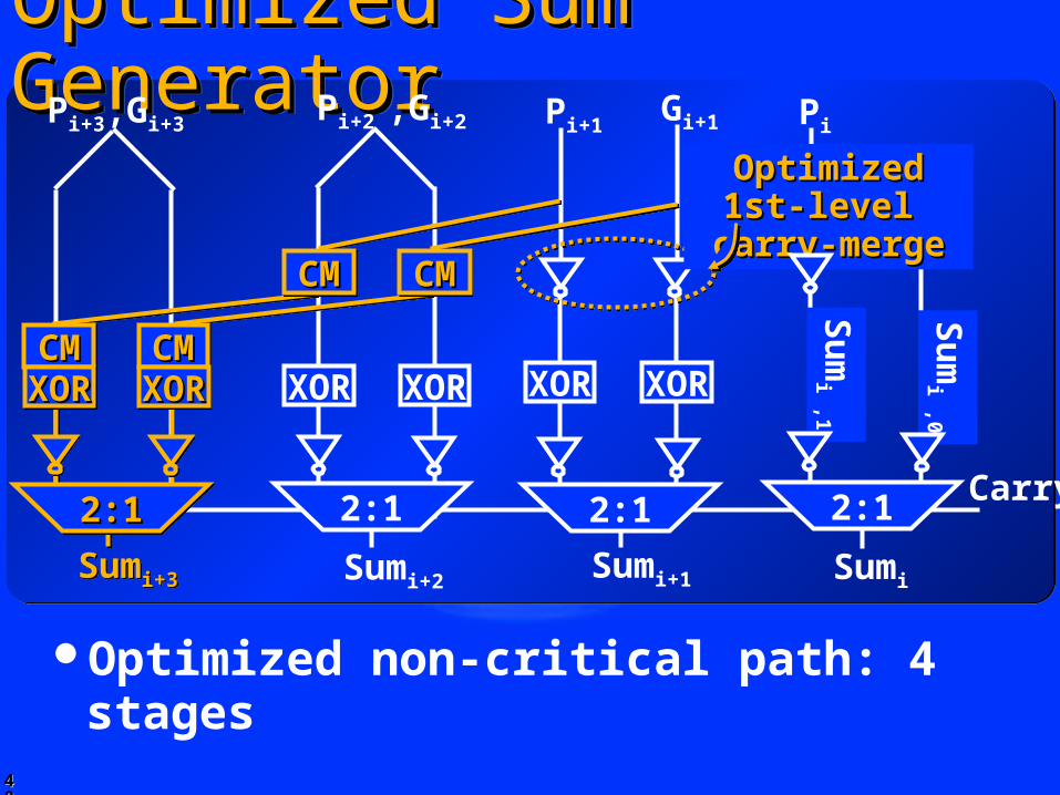
Optimized Sum GeneratorOptimized Sum GeneratorOptimized Sum GeneratorOptimized Sum GeneratorPi Pi+1
Pi+2 ,Gi+2
Sumi+1Sumi+2Sumi+3Sumi+3
XOR XORXOR XOR
Pi+3,Gi+3
Sumi
Su
mi ,1
Su
mi ,0
Carry
Gi+1
CMCMCMCM CMCMCMCM
Optimized 1st-level Optimized 1st-level carry-mergecarry-merge
Optimized non-critical path: 4 stages
2:1 2:1 2:12:12:12:12:1
CMCMCMCM CMCMCMCMXORXORXORXOR XORXORXORXOR