Embed Size (px)
Citation preview
This article was downloaded by: 10.3.98.104On: 13 Mar 2022Access details: subscription numberPublisher: CRC PressInforma Ltd Registered in England and Wales Registered Number: 1072954 Registered office: 5 Howick Place, London SW1P 1WG, UK
1 Handbook of NanophysicsPrinciples and MethodsKlaus D. Sattler
Tools for Predicting the Properties of Nanomaterials
Publication detailshttps://www.routledgehandbooks.com/doi/10.1201/9781420075410-5
James R. ChelikowskyPublished online on: 17 Sep 2010
How to cite :- James R. Chelikowsky. 17 Sep 2010, Tools for Predicting the Properties ofNanomaterials from: 1 Handbook of Nanophysics, Principles and Methods CRC PressAccessed on: 13 Mar 2022https://www.routledgehandbooks.com/doi/10.1201/9781420075410-5
PLEASE SCROLL DOWN FOR DOCUMENT
Full terms and conditions of use: https://www.routledgehandbooks.com/legal-notices/terms
This Document PDF may be used for research, teaching and private study purposes. Any substantial or systematic reproductions,re-distribution, re-selling, loan or sub-licensing, systematic supply or distribution in any form to anyone is expressly forbidden.
The publisher does not give any warranty express or implied or make any representation that the contents will be complete oraccurate or up to date. The publisher shall not be liable for an loss, actions, claims, proceedings, demand or costs or damageswhatsoever or howsoever caused arising directly or indirectly in connection with or arising out of the use of this material.
Dow
nloa
ded
By:
10.
3.98
.104
At:
09:3
0 13
Mar
202
2; F
or: 9
7814
2007
5410
, cha
pter
3, 1
0.12
01/9
7814
2007
5410
-5
3-1
3.1 Introduction
Materials at the nanoscale have been the subject of intensive study owing to their unusual electrical, magnetic, and optical proper-ties [1–9]. Th e combination of new synthesis techniques off ers unprecedented opportunities to tailor systems without resort to changing their chemical makeup. In particular, the physical properties of the material can be modifi ed by confi nement. If we confi ne a material in three, two, or one dimensions, we cre-ate a nanocrystal, a nanowire, or a nanofi lm, respectively. Such confi ned systems oft en possess dramatically diff erent properties than their macroscopic counterparts. As an example, consider the optical properties of the semiconductor cadmium selenide. By creating nanocrystals of diff erent sizes, typically ∼5 nm in diameter, the entire optical spectrum can be spanned. Likewise, silicon can be changed from an optically inactive material at the macroscopic scale to an optically active nanocrystal.
Th e physical confi nement of a material changes its proper-ties when the confi nement length is comparable to the quantum length scale. Th is can easily be seen by considering the uncer-tainty principle. At best, the uncertainty of a particle’s momen-tum, Δp, and its position, Δx, must be such that ΔpΔx ∼ ћ, where h is Planck’s constant divided by 2π. For a particle in a box of length scale, Δx, the kinetic energy of the particle will scale as ∼1/Δx2 and rapidly increase for small values of Δx. If the electron confi nement energy becomes comparable to the total energy of the electron, then its physical properties will clearly change, i.e., once the confi ning dimension approaches the delocalization length of an electron in a solid, “quantum confi nement” occurs.
We can restate this notion in a similar context by estimating a confi nement length, which can vary from solid to solid, and by
considering the wave properties of the electron. For example, the de Broglie wavelength of an electron is given by λ = h/p. If λ is in the order of Δx, then we expect confi nement and quantum eff ects to be important. Of course, this is essentially the same criterion from the uncertainty principle as λ ∼ Δx would give ΔpΔx ∼ h with p ∼ Δp. For a simple metal, we can estimate the momentum from a free electron gas: p = ћkf. kf is the wave vector such that the Fermi energy, 2 2
f f /2E k m= � . Th is yields kf = (3π2n)1/3 where n is the electron density. Th e value of kf for a typical simple metal such as Na is ∼1010 m−1. Th is would give a value of λ = h/p = 2π/kf or roughly ∼1 nm. We would expect quantum confi nement to occur on a length scale of a nanometer for this example.
To observe the role of quantum confi nement in real materials, we need to be able to construct materials routinely on the nano-meter scale. Th is is the case for many materials. Nanocrystals of many materials can be made, although sometimes it is diffi cult to determine whether crystallinity is preserved. Such nanostruc-tures provide a unique opportunity to study the properties at nanometer scales and to reveal the underlying physics occurring at reduced dimensionality. From a practical point of view, nano-structures are promising building blocks in nanotechnologies, e.g., the smallest nominal length scale in a modern CPU chip is in the order of 100 nm or less. At length scales less than this, the “band structure” of a material may no longer appear to be quasi-continuous. Rather the electronic energy levels may be described by discrete quantum energy levels, which change with the size of the system.
An understanding of the physics of confi nement is necessary to provide the fundamental science for the development of nano optical, magnetic, and electronic device applications. Th is understanding can best be obtained by utilizing ab initio
3Tools for Predicting the
Properties of Nanomaterials
3.1 Introduction .............................................................................................................................3-13.2 Th e Quantum Problem ...........................................................................................................3-2
Constructing Pseudopotentials from Density Functional Th eory • Algorithms for Solving the Kohn–Sham Equation
3.3 Applications ..............................................................................................................................3-7Silicon Nanocrystals • Iron Nanocrystals
3.4 Conclusions............................................................................................................................. 3-18Acknowledgments .............................................................................................................................3-19References ...........................................................................................................................................3-19
James R. ChelikowskyUniversity of Texas at Austin
Dow
nloa
ded
By:
10.
3.98
.104
At:
09:3
0 13
Mar
202
2; F
or: 9
7814
2007
5410
, cha
pter
3, 1
0.12
01/9
7814
2007
5410
-53-2 Handbook of Nanophysics: Principles and Methods
approaches [10]. Th ese approaches can provide valuable insights into nanoscale phenomena without empirical parameters or adjustments extrapolated from bulk properties [11,12]. As recently as 15 years ago, it was declared that ab initio approaches would not be useful to systems with more than a hundred atoms or so [11,12]. Of course, hardware advances have occurred since the mid-1990s, but more signifi cant advances have occurred in the area of algorithms and new ideas. Th ese ideas have allowed one to progress at a much faster rate than suggested by Moore’s law. We will review some of these advances and illustrate their application to nanocrystals. We will focus on two examples: a silicon nanocrystal and an iron nanocrystal. Th ese two exam-ples will illustrate the behavior of quantum confi nement on the optical gap in a semiconductor and on the magnetic moment of a ferromagnetic metal.
3.2 The Quantum Problem
Th e spatial and energetic distributions of electrons with the quantum theory of materials can be described by a solution of the Kohn–Sham eigenvalue equation [13], which can be justifi ed using density functional theory [13,14]:
ext H xc
2 2
( ) ( ) ( ) ( ) ( )2 n n nV r V r V r r E r
m⎡ ⎤− ∇ + + + Ψ = Ψ⎢ ⎥⎣ ⎦
� � � � �� (3.1)
where m is the electron mass. Th e eigenvalues correspond to energy levels, En, and the eigenfunctions or wave functions are given by Ψn; a solution of the Kohn–Sham equation gives the energetic and spatial distribution of the electrons. Th e exter-nal potential, Vext, is a potential that does not depend on the electronic solution. Th e external potential can be taken as a linear superposition of atomic potentials corresponding to the Coulomb potential produced by the nuclear charge. In the case of an isolated hydrogen atom, Vext = −e2/r. Th e potential arising from the electron–electron interactions can be divided into two parts. One part represents the “classical” electrostatic terms and is called the “Hartree” or “Coulomb” potential:
H2 ( ) 4V r e r∇ = − π ρ( )� �
(3.2)
where ρ is the electron charge density; it is obtained by summing up the square of the occupied eigenfunctions and gives the prob-ability of fi nding an electron at the point r→
occup
2
,
( )n
n
r e rρ( ) = Ψ∑� � (3.3)
The second part of the screening potential, the “exchange-correlation” part of the potential, Vxc, is quantum mechani-cal in nature and eff ectively contains the physics of the Pauli exclusion principle. A common approximation for this part of the potential arises from the local density approximation, i.e.,
the potential depends only on the charge density at the point of interest, Vxc(r
→) = Vxc[ρ(r→)].In principle, the density functional theory is exact, provided
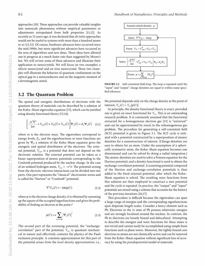
one is given an exact functional for Vxc. Th is is an outstanding research problem. It is commonly assumed that the functional extracted for a homogeneous electron gas [15] is “universal” and can be approximated by resort to the inhomogeneous gas problem. Th e procedure for generating a self-consistent fi eld (SCF) potential is given in Figure 3.1. Th e SCF cycle is initi-ated with a potential constructed by a superposition of atomic densities for a nanostructure of interest. (Charge densities are easy to obtain for an atom. Under the assumption of a spheri-cally symmetric atom, the Kohn–Sham equation becomes one dimensional and can be solved by doing a radial integration.) Th e atomic densities are used to solve a Poisson equation for the Hartree potential, and a density functional is used to obtain the exchange-correlation potential. A screening potential composed of the Hartree and exchange-correlation potentials is then added to the fi xed external potential, aft er which the Kohn–Sham equation is solved. Th e resulting wave functions from this solution are then employed to construct a new potential and the cycle is repeated. In practice, the “output” and “input” potentials are mixed using a scheme that accounts for the history of the previous iterations [16,17].
Th is procedure is diffi cult because the eigenvalues can span a large range of energies and the corresponding eigenfunctions span disparate length scales. Consider a heavy element such as Pb. Electrons in the 1s state of Pb possess relativistic energies and are strongly localized around the nucleus. In contrast, the Pb 6s electrons are loosely bound and delocalized. Attempting to describe the energies and wave functions for these states is not trivial and cannot easily be accomplished using simple basis functions such as plane waves. Moreover, the tightly bound core electrons in atoms are not chemically active and can be removed from the Kohn–Sham equation without signifi cant loss of accu-racy by using the pseudopotential model of materials.
Assume initial density: ρ
Solve: Δ2VH= –4πeρ
Form: VT = V pion +VH +Vxc
V pion +VH +VxcSolve: –ћ2 Δ2
2m Ψn = EnΨn
Form: ρ = e |Ψn|2n, occup
FIGURE 3.1 Self-consistent fi eld loop. Th e loop is repeated until the “input” and “output” charge densities are equal to within some speci-fi ed tolerance.

Dow
nloa
ded
By:
10.
3.98
.104
At:
09:3
0 13
Mar
202
2; F
or: 9
7814
2007
5410
, cha
pter
3, 1
0.12
01/9
7814
2007
5410
-5Tools for Predicting the Properties of Nanomaterials 3-3
Th e pseudopotential model is quite general and refl ects the physical content of the periodic table. In Figure 3.2, the pseu-dopotential model is illustrated for a crystal. In the pseudopo-tential model of a material, the electron states are decomposed into core states and valence states, e.g., in silicon the 1s22s22p6 states represent the core states, and the 3s23p2 states represent the valence states. Th e pseudopotential represents the potential arising from a combination of core states and the nuclear charge: the so-called ion-core pseudopotential. Th e ion-core pseudopo-tential is assumed to be completely transferable from the atom to a cluster or to a nanostructure.
By replacing the external potential in the Kohn–Sham equation with an ion-core pseudopotential, we can avoid considering the core states altogether. Th e solution of the Kohn–Sham equation using pseudopotentials will yield only the valence states. Th e energy and length scales are then set by the valence states; it becomes no more diffi cult to solve for the electronic states of a heavy element such as Pb when compared to a light element such as C.
3.2.1 Constructing Pseudopotentials from Density Functional Theory
Here we will focus on recipes for creating ion-core pseudopoten-tials within the density functional theory, although pseudopo-tentials can also be constructed from experimental data [18]. Th e construction of ion-core pseudopotentials has become an active area of electronic structure theory. Methods for constructing such potentials have centered on ab initio or “fi rst-principles” pseudopo-tentials; i.e., the informational content on which the pseudopoten-tial is based does not involve any experimental input.
Th e fi rst step in the construction process is to consider an electronic structure calculation for a free atom. For example, in the case of a silicon atom the Kohn–Sham equation [13] can be solved for the eigenvalues and wave functions. Knowing the
valence wave functions, i.e., 3s2 and 3p2, states and correspond-ing eigenvalues, the pseudo wave functions can be constructed. Solving the Kohn–Sham problem for an atom is an easy numeri-cal calculation as the atomic densities are assumed to possess spherical symmetry and the problem reduces to a one-dimen-sional radial integration. Once we know the solution for an “all-electron” potential, we can invert the Kohn–Sham equation and fi nd the total pseudopotential. We can “unscreen” the total potential and extract the ion-core pseudopotential. Th is ion-core potential, which arises from tightly bound core electrons and the nuclear charge, is not expected to change from one environment to another. Th e issue of this “transferability” is one that must be addressed according to the system of interest. Th e immediate issue is how to defi ne pseudo-wave functions that can be used to defi ne the corresponding pseudopotential.
Suppose we insist that the pseudo-wave function be identical to the all-electron wave function outside of the core region. For example, let us consider the 3s state for a silicon atom. We want the pseudo-wave function to be identical to the all-electron state outside the core region:
c3 3( ) ( )s sr r r rφ = ψ >p (3.4)
where3sφ p is a pseudo-wave function for the 3s state
rc defi nes the core size
Th is assignment will guarantee that the pseudo-wave func-tion will possess properties identical to the all-electron wave function, ψ3s, in the region away from the ion core.
For r < rc, we alter the all-electron wave function. We are free to do this as we do not expect the valence wave function within the core region to alter the chemical properties of the system. We choose to make the pseudo-wave function smooth and nodeless in the core region. Th is initiative will provide rapid convergence with simple basis functions. One other criterion is mandated. Namely, the integral of the pseudocharge density within the core should be equal to the integral of the all-electron charge density. Without this condition, the pseudo-wave function dif-fers by a scaling factor from the all-electron wave function. Pseudopotentials constructed with this constraint are called “norm conserving” [19]. Since we expect the bonding in a solid to be highly dependent on the tails of the valence wave func-tions, it is imperative that the normalized pseudo-wave function be identical to the all-electron wave functions.
Th ere are many ways of constructing “norm-conserving” pseudopotentials as within the core the pseudo-wave function is not unique. One of the most straightforward construction pro-cedures is from Kerker [20] and was later extended by Troullier and Martins [21].
c
c
exp( ( ))( )
( )
lpl
l
r p r r rr
r r r⎧ ≤⎪φ = ⎨ψ >⎪⎩
(3.5)
NucleusCore electronsValence electrons
FIGURE 3.2 Pseudopotential model of a solid.
Dow
nloa
ded
By:
10.
3.98
.104
At:
09:3
0 13
Mar
202
2; F
or: 9
7814
2007
5410
, cha
pter
3, 1
0.12
01/9
7814
2007
5410
-53-4 Handbook of Nanophysics: Principles and Methods
p(r) is taken to be a polynomial of the form
6
20 2
1
( ) nn
n
p r c c r=
= + ∑ (3.6)
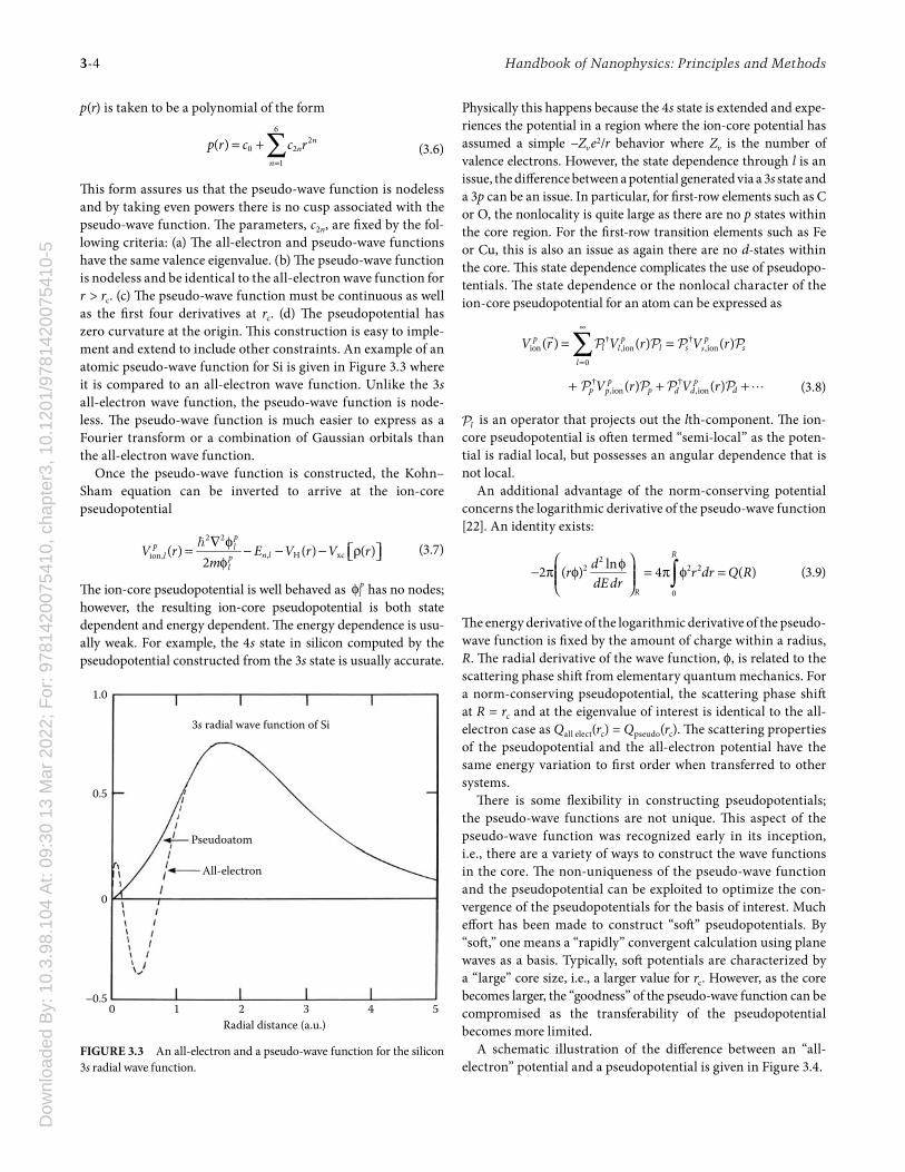
Th is form assures us that the pseudo-wave function is nodeless and by taking even powers there is no cusp associated with the pseudo-wave function. Th e parameters, c2n, are fi xed by the fol-lowing criteria: (a) Th e all-electron and pseudo-wave functions have the same valence eigenvalue. (b) Th e pseudo-wave function is nodeless and be identical to the all-electron wave function for r > rc. (c) Th e pseudo-wave function must be continuous as well as the fi rst four derivatives at rc. (d) Th e pseudopotential has zero curvature at the origin. Th is construction is easy to imple-ment and extend to include other constraints. An example of an atomic pseudo-wave function for Si is given in Figure 3.3 where it is compared to an all-electron wave function. Unlike the 3s all-electron wave function, the pseudo-wave function is node-less. Th e pseudo-wave function is much easier to express as a Fourier transform or a combination of Gaussian orbitals than the all-electron wave function.
Once the pseudo-wave function is constructed, the Kohn–Sham equation can be inverted to arrive at the ion-core pseudopotential
2 2
, H xcion, ( ) ( ) ( )2
pp l
n ll pl
V r E V r V rm∇ φ= − − − ρ⎡ ⎤⎣ ⎦φ� (3.7)
Th e ion-core pseudopotential is well behaved as plφ has no nodes;
however, the resulting ion-core pseudopotential is both state dependent and energy dependent. Th e energy dependence is usu-ally weak. For example, the 4s state in silicon computed by the pseudopotential constructed from the 3s state is usually accurate.
Physically this happens because the 4s state is extended and expe-riences the potential in a region where the ion-core potential has assumed a simple −Zv e2/r behavior where Zv is the number of valence electrons. However, the state dependence through l is an issue, the diff erence between a potential generated via a 3s state and a 3p can be an issue. In particular, for fi rst-row elements such as C or O, the nonlocality is quite large as there are no p states within the core region. For the fi rst-row transition elements such as Fe or Cu, this is also an issue as again there are no d-states within the core. Th is state dependence complicates the use of pseudopo-tentials. Th e state dependence or the nonlocal character of the ion-core pseudopotential for an atom can be expressed as
†ion ion ion
† †ion ion
†, ,
0
, ,
( ) ( ) ( )
( ) ( )
p p pl l s sl s
l
p pp p dp d d
V r V r V r
V r V r
∞
=
= =
+ + +
∑�
�
P P P P
P P P P (3.8)
lP is an operator that projects out the lth-component. Th e ion-core pseudopotential is oft en termed “semi-local” as the poten-tial is radial local, but possesses an angular dependence that is not local.
An additional advantage of the norm-conserving potential concerns the logarithmic derivative of the pseudo-wave function [22]. An identity exists:
2
2 2 2
0
ln2 ( ) 4 ( )R
R
dr r dr Q RdE dr
⎛ ⎞φ− π φ = π φ =⎜ ⎟⎜ ⎟⎝ ⎠ ∫ (3.9)
Th e energy derivative of the logarithmic derivative of the pseudo-wave function is fi xed by the amount of charge within a radius, R. Th e radial derivative of the wave function, ϕ, is related to the scattering phase shift from elementary quantum mechanics. For a norm-conserving pseudopotential, the scattering phase shift at R = rc and at the eigenvalue of interest is identical to the all-electron case as Qall elect(rc) = Qpseudo(rc). Th e scattering properties of the pseudopotential and the all-electron potential have the same energy variation to fi rst order when transferred to other systems.
Th ere is some fl exibility in constructing pseudopotentials; the pseudo-wave functions are not unique. Th is aspect of the pseudo-wave function was recognized early in its inception, i.e., there are a variety of ways to construct the wave functions in the core. Th e non-uniqueness of the pseudo-wave function and the pseudopotential can be exploited to optimize the con-vergence of the pseudopotentials for the basis of interest. Much eff ort has been made to construct “soft ” pseudopotentials. By “soft ,” one means a “rapidly” convergent calculation using plane waves as a basis. Typically, soft potentials are characterized by a “large” core size, i.e., a larger value for rc. However, as the core becomes larger, the “goodness” of the pseudo-wave function can be compromised as the transferability of the pseudopotential becomes more limited.
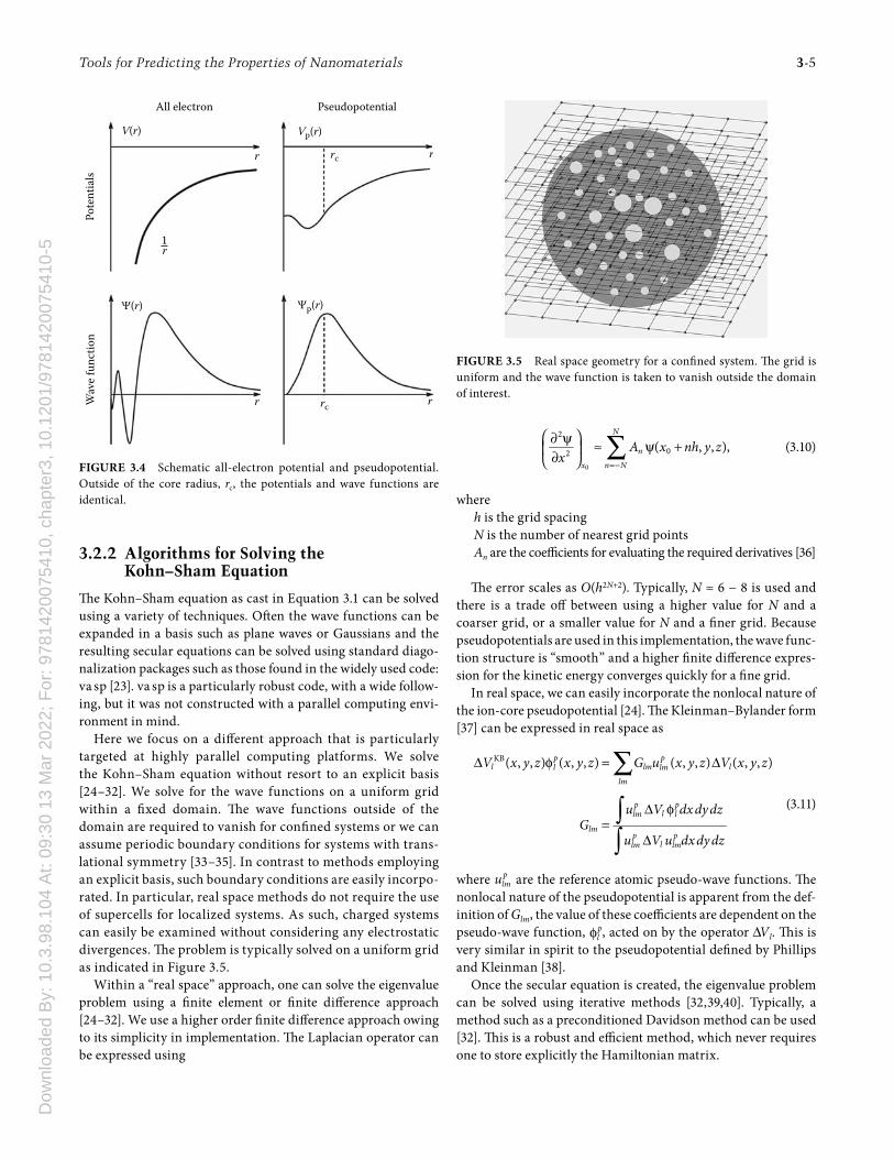
A schematic illustration of the diff erence between an “all-electron” potential and a pseudopotential is given in Figure 3.4.
1.0
0
–0.50 1 2
Radial distance (a.u.)
All-electron
Pseudoatom
3s radial wave function of Si
3 4 5
0.5
FIGURE 3.3 An all-electron and a pseudo-wave function for the silicon 3s radial wave function.
Dow
nloa
ded
By:
10.
3.98
.104
At:
09:3
0 13
Mar
202
2; F
or: 9
7814
2007
5410
, cha
pter
3, 1
0.12
01/9
7814
2007
5410
-5Tools for Predicting the Properties of Nanomaterials 3-5
3.2.2 Algorithms for Solving the Kohn–Sham Equation
Th e Kohn–Sham equation as cast in Equation 3.1 can be solved using a variety of techniques. Oft en the wave functions can be expanded in a basis such as plane waves or Gaussians and the resulting secular equations can be solved using standard diago-nalization packages such as those found in the widely used code: va sp [23]. va sp is a particularly robust code, with a wide follow-ing, but it was not constructed with a parallel computing envi-ronment in mind.
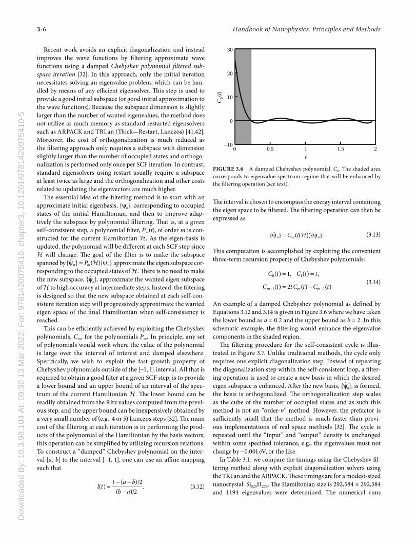
Here we focus on a diff erent approach that is particularly targeted at highly parallel computing platforms. We solve the Kohn–Sham equation without resort to an explicit basis [24–32]. We solve for the wave functions on a uniform grid within a fi xed domain. Th e wave functions outside of the domain are required to vanish for confi ned systems or we can assume periodic boundary conditions for systems with trans-lational symmetry [33–35]. In contrast to methods employing an explicit basis, such boundary conditions are easily incorpo-rated. In particular, real space methods do not require the use of supercells for localized systems. As such, charged systems can easily be examined without considering any electrostatic divergences. Th e problem is typically solved on a uniform grid as indicated in Figure 3.5.
Within a “real space” approach, one can solve the eigenvalue problem using a fi nite element or fi nite diff erence approach [24–32]. We use a higher order fi nite diff erence approach owing to its simplicity in implementation. Th e Laplacian operator can be expressed using
0
2
02 ( , , ),N
n
n Nx
A x nh y zx
=−
⎛ ⎞∂ ψ ≈ ψ +⎜ ⎟∂⎝ ⎠∑ (3.10)
whereh is the grid spacingN is the number of nearest grid pointsAn are the coeffi cients for evaluating the required derivatives [36]
Th e error scales as O(h2N+2). Typically, N ≈ 6 − 8 is used and there is a trade off between using a higher value for N and a coarser grid, or a smaller value for N and a fi ner grid. Because pseudopotentials are used in this implementation, the wave func-tion structure is “smooth” and a higher fi nite diff erence expres-sion for the kinetic energy converges quickly for a fi ne grid.
In real space, we can easily incorporate the nonlocal nature of the ion-core pseudopotential [24]. Th e Kleinman–Bylander form [37] can be expressed in real space as
KB( , , ) ( , , ) ( , , ) ( , , )p pl lm ll lm
lm
p pllm l
lmp p
llm lm
V x y z x y z G u x y z V x y z
u V dx dy dzG
u V u dx dy dz
Δ φ = Δ
Δ φ=
Δ
∑
∫∫
(3.11)
where plmu are the reference atomic pseudo-wave functions. Th e
nonlocal nature of the pseudopotential is apparent from the def-inition of Glm, the value of these coeffi cients are dependent on the pseudo-wave function, p
lφ , acted on by the operator ΔVl. Th is is very similar in spirit to the pseudopotential defi ned by Phillips and Kleinman [38].
Once the secular equation is created, the eigenvalue problem can be solved using iterative methods [32,39,40]. Typically, a method such as a preconditioned Davidson method can be used [32]. Th is is a robust and effi cient method, which never requires one to store explicitly the Hamiltonian matrix.
All electron PseudopotentialPo
tentials
Wave f
unction
V(r)
Ψ(r)
Vp(r)
Ψp(r)
rc
rc r
rr
r
1r
FIGURE 3.4 Schematic all-electron potential and pseudopotential. Outside of the core radius, rc, the potentials and wave functions are identical.
FIGURE 3.5 Real space geometry for a confi ned system. Th e grid is uniform and the wave function is taken to vanish outside the domain of interest.
Dow
nloa
ded
By:
10.
3.98
.104
At:
09:3
0 13
Mar
202
2; F
or: 9
7814
2007
5410
, cha
pter
3, 1
0.12
01/9
7814
2007
5410
-53-6 Handbook of Nanophysics: Principles and Methods
Recent work avoids an explicit diagonalization and instead improves the wave functions by fi ltering approximate wave functions using a damped Chebyshev polynomial fi ltered sub-space iteration [32]. In this approach, only the initial iteration necessitates solving an eigenvalue problem, which can be han-dled by means of any effi cient eigensolver. Th is step is used to provide a good initial subspace (or good initial approximation to the wave functions). Because the subspace dimension is slightly larger than the number of wanted eigenvalues, the method does not utilize as much memory as standard restarted eigensolvers such as ARPACK and TRLan (Th ick—Restart, Lanczos) [41,42]. Moreover, the cost of orthogonalization is much reduced as the fi ltering approach only requires a subspace with dimension slightly larger than the number of occupied states and orthogo-nalization is performed only once per SCF iteration. In contrast, standard eigensolvers using restart usually require a subspace at least twice as large and the orthogonalization and other costs related to updating the eigenvectors are much higher.
Th e essential idea of the fi ltering method is to start with an approximate initial eigenbasis, {ψn}, corresponding to occupied states of the initial Hamiltonian, and then to improve adap-tively the subspace by polynomial fi ltering. Th at is, at a given self- consistent step, a polynomial fi lter, Pm(t), of order m is con-structed for the current Hamiltonian H. As the eigen-basis is updated, the polynomial will be diff erent at each SCF step since H will change. Th e goal of the fi lter is to make the subspace spanned by ˆ{ } ( ){ }n m nPψ = ψH approximate the eigen subspace cor-responding to the occupied states of H. Th ere is no need to make the new subspace, {ψ̂n}, approximate the wanted eigen subspace of H to high accuracy at intermediate steps. Instead, the fi ltering is designed so that the new subspace obtained at each self-con-sistent iteration step will progressively approximate the wanted eigen space of the fi nal Hamiltonian when self-consistency is reached.
Th is can be effi ciently achieved by exploiting the Chebyshev polynomials, Cm, for the polynomials Pm. In principle, any set of polynomials would work where the value of the polynomial is large over the interval of interest and damped elsewhere. Specifi cally, we wish to exploit the fast growth property of Chebyshev polynomials outside of the [−1, 1] interval. All that is required to obtain a good fi lter at a given SCF step, is to provide a lower bound and an upper bound of an interval of the spec-trum of the current Hamiltonian H. Th e lower bound can be readily obtained from the Ritz values computed from the previ-ous step, and the upper bound can be inexpensively obtained by a very small number of (e.g., 4 or 5) Lanczos steps [32]. Th e main cost of the fi ltering at each iteration is in performing the prod-ucts of the polynomial of the Hamiltonian by the basis vectors; this operation can be simplifi ed by utilizing recursion relations. To construct a “damped” Chebyshev polynomial on the inter-val [a, b] to the interval [−1, 1], one can use an affi ne mapping such that
( )/2
( ) .( )/2
t a bl t
b a− +
=−
(3.12)
Th e interval is chosen to encompass the energy interval containing the eigen space to be fi ltered. Th e fi ltering operation can then be expressed as
ˆ{ } ( ( )){ }.n m nC lψ = ψH (3.13)
Th is computation is accomplished by exploiting the convenient three-term recursion property of Chebyshev polynomials:
+ −
= =
= −
0 1
1 1
( ) 1, ( ) ,
( ) 2 ( ) ( )m m m
C t C t t
C t t C t C t (3.14)
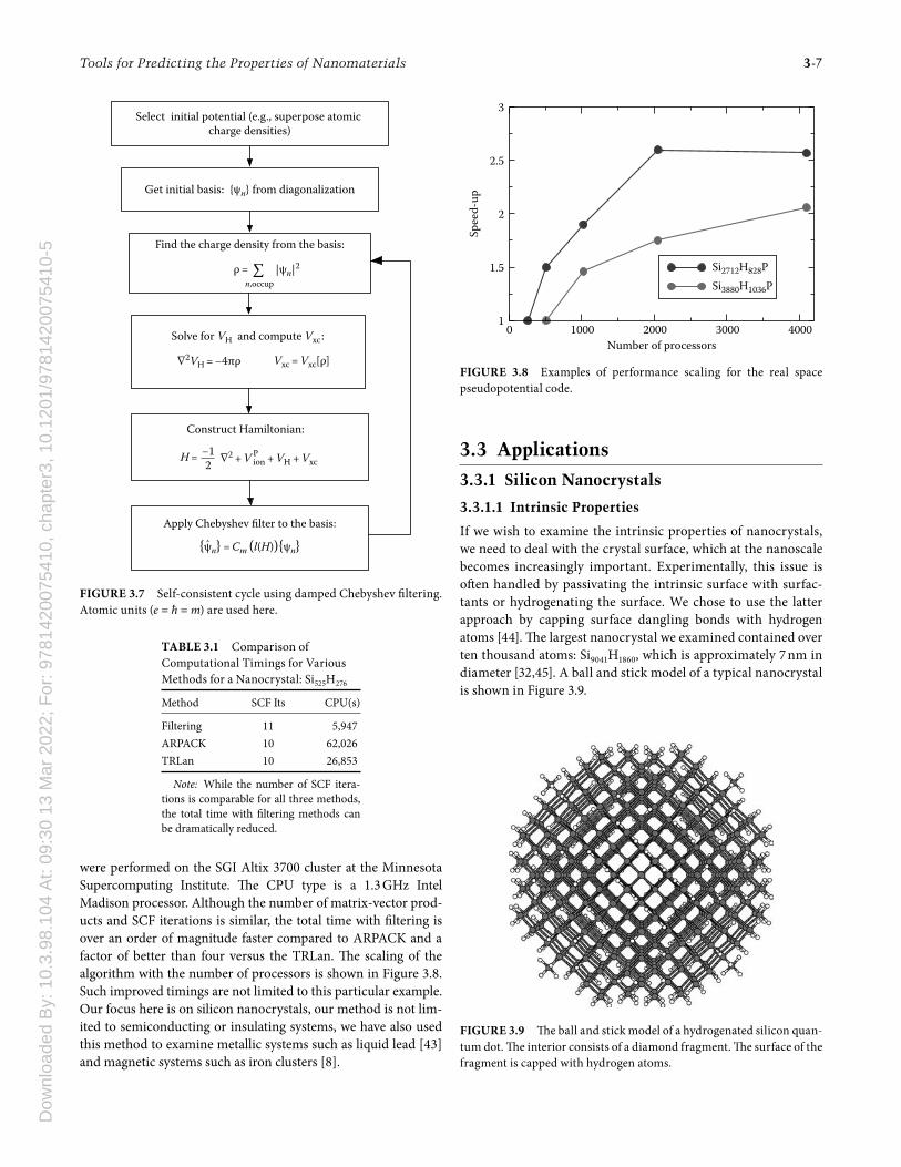
An example of a damped Chebyshev polynomial as defi ned by Equations 3.12 and 3.14 is given in Figure 3.6 where we have taken the lower bound as a = 0.2 and the upper bound as b = 2. In this schematic example, the fi ltering would enhance the eigenvalue components in the shaded region.
Th e fi ltering procedure for the self-consistent cycle is illus-trated in Figure 3.7. Unlike traditional methods, the cycle only requires one explicit diagonalization step. Instead of repeating the diagonalization step within the self-consistent loop, a fi lter-ing operation is used to create a new basis in which the desired eigen subspace is enhanced. Aft er the new basis, {ψ̂n}, is formed, the basis is orthogonalized. Th e orthogonalization step scales as the cube of the number of occupied states and as such this method is not an “order-n” method. However, the prefactor is suffi ciently small that the method is much faster than previ-ous implementations of real space methods [32]. Th e cycle is repeated until the “input” and “output” density is unchanged within some specifi ed tolerance, e.g., the eigenvalues must not change by ∼0.001 eV, or the like.
In Table 3.1, we compare the timings using the Chebyshev fi l-tering method along with explicit diagonalization solvers using the TRLan and the ARPACK. Th ese timings are for a modest-sized nanocrystal: Si525H276. Th e Hamiltonian size is 292,584 × 292,584 and 1194 eigenvalues were determined. Th e numerical runs
30
20
C 6(l) 10
0
–100 0.5 1
t1.5 2
FIGURE 3.6 A damped Chebyshev polynomial, C6. Th e shaded area corresponds to eigenvalue spectrum regime that will be enhanced by the fi ltering operation (see text).
Dow
nloa
ded
By:
10.
3.98
.104
At:
09:3
0 13
Mar
202
2; F
or: 9
7814
2007
5410
, cha
pter
3, 1
0.12
01/9
7814
2007
5410
-5Tools for Predicting the Properties of Nanomaterials 3-7
were performed on the SGI Altix 3700 cluster at the Minnesota Supercomputing Institute. Th e CPU type is a 1.3 GHz Intel Madison processor. Although the number of matrix-vector prod-ucts and SCF iterations is similar, the total time with fi ltering is over an order of magnitude faster compared to ARPACK and a factor of better than four versus the TRLan. Th e scaling of the algorithm with the number of processors is shown in Figure 3.8. Such improved timings are not limited to this particular example. Our focus here is on silicon nanocrystals, our method is not lim-ited to semiconducting or insulating systems, we have also used this method to examine metallic systems such as liquid lead [43] and magnetic systems such as iron clusters [8].
3.3 Applications
3.3.1 Silicon Nanocrystals
3.3.1.1 Intrinsic Properties
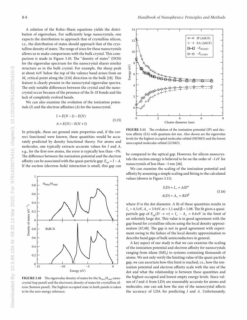
If we wish to examine the intrinsic properties of nanocrystals, we need to deal with the crystal surface, which at the nanoscale becomes increasingly important. Experimentally, this issue is oft en handled by passivating the intrinsic surface with surfac-tants or hydrogenating the surface. We chose to use the latter approach by capping surface dangling bonds with hydrogen atoms [44]. Th e largest nanocrystal we examined contained over ten thousand atoms: Si9041H1860, which is approximately 7 nm in diameter [32,45]. A ball and stick model of a typical nanocrystal is shown in Figure 3.9.
Select initial potential (e.g., superpose atomic charge densities)
Get initial basis: {ψn} from diagonalization
Find the charge density from the basis:
n,occup∑ρ = |ψn|2
Solve for VH and compute Vxc:
Δ2VH = −4πρ Vxc = Vxc[ρ]
Construct Hamiltonian:
H = −12
Δ2 + V Pion + VH + Vxc
Apply Chebyshev filter to the basis:
ˆ{ψn} = Cm (l(H)){ψn}
FIGURE 3.7 Self-consistent cycle using damped Chebyshev fi ltering. Atomic units (e = ћ = m) are used here.
TABLE 3.1 Comparison of Computational Timings for Various Methods for a Nanocrystal: Si525H276
Method SCF Its CPU(s)
Filtering 11 5,947ARPACK 10 62,026TRLan 10 26,853
Note: While the number of SCF itera-tions is comparable for all three methods, the total time with fi ltering methods can be dramatically reduced.
0 1000 2000 3000 4000Number of processors
1
1.5
2
2.5
3
Spee
d-up
Si2712H828PSi3880H1036P
FIGURE 3.8 Examples of performance scaling for the real space pseudopotential code.
FIGURE 3.9 Th e ball and stick model of a hydrogenated silicon quan-tum dot. Th e interior consists of a diamond fragment. Th e surface of the fragment is capped with hydrogen atoms.
Dow
nloa
ded
By:
10.
3.98
.104
At:
09:3
0 13
Mar
202
2; F
or: 9
7814
2007
5410
, cha
pter
3, 1
0.12
01/9
7814
2007
5410
-53-8 Handbook of Nanophysics: Principles and Methods
A solution of the Kohn–Sham equations yields the distri-bution of eigenvalues. For suffi ciently large nanocrystals, one expects the distribution to approach that of crystalline silicon, i.e., the distribution of states should approach that of the crys-talline density of states. Th e range of sizes for these nanocrystals allows us to make comparisons with the bulk crystal. Th is com-parison is made in Figure 3.10. Th e “density of states” (DOS) for the eigenvalue spectrum for the nanocrystal shares similar structure as in the bulk crystal. For example, the sharp peak at about 4 eV below the top of the valence band arises from an M1 critical point along the [110] direction in the bulk [18]. Th is feature is clearly present in the nanocrystal eigenvalue spectra. Th e only notable diff erences between the crystal and the nano-crystal occur because of the presence of the Si–H bonds and the lack of completely evolved bands.
We can also examine the evolution of the ionization poten-tials (I) and the electron affi nities (A) for the nanocrystal.
( 1) ( )
( ) ( 1)
I E N E N
A E N E N
= − −
= − + (3.15)
In principle, these are ground state properties and, if the cor-rect functional were known, these quantities would be accu-rately predicted by density functional theory. For atoms and molecules, one typically extracts accurate values for I and A, e.g., for the fi rst-row atoms, the error is typically less than ∼5%. Th e diff erence between the ionization potential and the electron affi nity can be associated with the quasi-particle gap: Eqp = I − A. If the exciton (electron–hole) interaction is small, this gap can
be compared to the optical gap. However, for silicon nanocrys-tals the exciton energy is believed to be on the order of ∼1 eV for nanocrystals of less than ∼1 nm [46].
We can examine the scaling of the ionization potential and affi nity by assuming a simple scaling and fi tting to the calculated values (shown in Figure 3.11):
( ) /
( ) /
I D I A D
A D A B D
α∞
β∞
= +
= + (3.16)
where D is the dot diameter. A fi t of these quantities results in I∞ = 4.5 eV, A∞ = 3.9 eV, α = 1.1 and β = 1.08. Th e fi t gives a quasi-particle gap of Eqp(D → ∞) = I∞ − A∞ = 0.6 eV in the limit of an infi nitely large dot. Th is value is in good agreement with the gap found for crystalline silicon using the local density approxi-mation [47,48]. Th e gap is not in good agreement with experi-ment owing to the failure of the local density approximation to describe band gaps of bulk semiconductors in general.
A key aspect of our study is that we can examine the scaling of the ionization potential and electron affi nity for nanocrystals ranging from silane (SiH4) to systems containing thousands of atoms. We not only verify the limiting value of the quasi-particle gap, we can ascertain how this limit is reached, i.e., how the ion-ization potential and electron affi nity scale with the size of the dot and what the relationship is between these quantities and the highest occupied and lowest empty energy levels. Since val-ues of I and A from LDA are reasonably accurate for atoms and molecules, one can ask how the size of the nanocrystal aff ects the accuracy of LDA for predicting I and A. Unfortunately,
–15 –10 –5 0Energy (eV)
0
0.2
0.4
0.6
0.8
0
0.2
0.4
0.6
0.8
1
Den
sity o
f sta
tes (
eV–1
)
Bulk Si
Si9041H1860
FIGURE 3.10 Th e eigenvalue density of states for the Si9041H1860 nano-crystal (top panel) and the electronic density of states for crystalline sil-icon (bottom panel). Th e highest occupied state in both panels is taken to be the zero energy reference.
0 2 4 6 8Cluster diameter (nm)
0
2
4
6
8
10
12
14
Ener
gy (e
V)
IP (ΔSCF)EA (ΔSCF)–EHOMO
–ELUMO
FIGURE 3.11 Th e evolution of the ionization potential (IP) and elec-tron affi nity (EA) with quantum dot size. Also shown are the eigenvalue levels for the highest occupied molecular orbital (HOMO) and the lowest unoccupied molecular orbital (LUMO).
Dow
nloa
ded
By:
10.
3.98
.104
At:
09:3
0 13
Mar
202
2; F
or: 9
7814
2007
5410
, cha
pter
3, 1
0.12
01/9
7814
2007
5410
-5Tools for Predicting the Properties of Nanomaterials 3-9
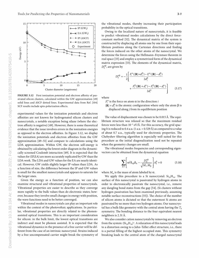
experimental values for the ionization potentials and electron affi nities are not known for hydrogenated silicon clusters and nanocrystals, a notable exception being silane (where the elec-tron affi nity is negative) [49]. However, there is some theoretical evidence that the issue involves errors in the ionization energies as opposed to the electron affi nities. In Figure 3.12, we display the ionization potentials and electron affi nities from the GW approximation [49–51] and compare to calculations using the LDA approximation. Within GW, the electron self-energy is obtained by calculating the lowest order diagram in the dynami-cally screened Coulomb interaction [49]. It is expected that the values for (IP,EA) are more accurately replicated by GW than the LDA work. Th e LDA and GW values for the EA are nearly identi-cal. However, GW yields slightly larger IP values than LDA. As a function of size, the diff erence between the IP and GW values is small for the smallest nanocrystals and appears to saturate for the larger ones.
Given the energy as a function of position, we can also examine structural and vibrational properties of nanocrystals. Vibrational properties are easier to describe as they converge more rapidly to the bulk values than do electronic states; how-ever, because they involve small changes in energy with position, the wave functions need to be better converged.
Vibrational modes in nanocrystals can play an important role within the context of the photovoltaic applications. In particu-lar, vibrational properties are directly related to the phonon-assisted optical transitions. Th is is an important consideration for silicon: in the bulk limit, the lowest optical transitions are indirect and must be phonon assisted. It is expected that the vibrational dynamics in the presence of a free carrier will be dif-ferent from the case of an intrinsic nanocrystal. Strains induced by a free uncompensated carrier might break the symmetry of
the vibrational modes, thereby increasing their participation probability in the optical transitions.
Owing to the localized nature of nanocrystals, it is feasible to predict vibrational modes calculations by the direct force-constant method [52]. Th e dynamical matrix of the system is constructed by displacing all atoms one by one from their equi-librium positions along the Cartesian directions and fi nding the forces induced on the other atoms of the nanocrystal. We determine the forces using the Hellmann–Feynman theorem in real space [33] and employ a symmetrized form of the dynamical matrix expression [53]. Th e elements of the dynamical matrix,
ijDαβ, are given by
({ }+ ) ({ } )12 2
({ } ) ({ } )2
i ij jij
j
i ij j
i
F F dD
d
F d F dd
β βα ααβ
β
β βα α
α
⎡ − −= − ⎢
⎢⎣
⎤+ − −+ ⎥
⎥⎦
R R
R R
d
(3.17)
wherejF α is the force on atom α in the direction i
{ } jdβ+R is the atomic confi guration where only the atom β is displaced along j from its equilibrium position
Th e value of displacement was chosen to be 0.015 Å. Th e equi-librium structure was relaxed so that the maximum residual forces were less than 10−3 eV/Å. For this accuracy, the grid spac-ing h is reduced to 0.4 a.u. (1 a.u. = 0.529 Å) as compared to a value of about 0.7 a.u., typically used for electronic properties. Th e Chebyshev fi ltering algorithm is especially well suited for this procedure as the initial diagonalization need not be repeated when the geometry changes are small.
Th e vibrational modes frequencies and corresponding eigen-vectors can be obtained from the dynamical equation
2
,
0ikik k
k
D AM Mα
αββ
αβββ
⎡ ⎤⎢ ⎥ω δ δ − =⎢ ⎥⎣ ⎦
∑ (3.18)
where Mα is the mass of atom labeled by α.We apply this procedure to a Si nanocrystal: Si29H36. Th e
surface of this nanocrystal is passivated by hydrogen atoms in order to electronically passivate the nanocrystal, i.e., remove any dangling bond states from the gap [54]. (Si clusters without hydrogen passivation has been examined previously, assuming notable surface reconstructions [55]). Th e choice of the number of silicon atoms is dictated so that the outermost Si atoms are passivated by no more than two hydrogen atoms. Our nanocrys-tal has a bulk-like geometry with the central atom having the Td symmetry. Th e bonding distance to the four equivalent nearest neighbors is 2.31 Å.
We also consider cation nanocrystals by removing an electron from the system: (Si29H36)+. A relaxation of this nanocrystal leads to a distortion owing to a Jahn–Teller eff ect structure, i.e., there is a partial fi lling of the highest occupied state. Th is symmetry breaking leads to the central atom of the charged nanocrystal
0 5 10 15 20Cluster diameter (angstroms)
0
5
10
15En
ergy
(eV
)
IP (GWf)
EA (GWf)
IP (ΔSCF)EA (ΔSCF)Experiment
FIGURE 3.12 First ionization potential and electron affi nity of pas-sivated silicon clusters, calculated within the GW approximation [49] solid lines and ΔSCF dotted lines. Experimental data from Ref. [104] SCF results include spin-polarization eff ects.
Dow
nloa
ded
By:
10.
3.98
.104
At:
09:3
0 13
Mar
202
2; F
or: 9
7814
2007
5410
, cha
pter
3, 1
0.12
01/9
7814
2007
5410
-53-10 Handbook of Nanophysics: Principles and Methods
being bonded to four atoms with diff erent bond lengths. Two bond lengths become slightly shorter (2.30 Å) and two others lengthen (2.35 Å). Th is distortion propagates throughout the nanocrystal.
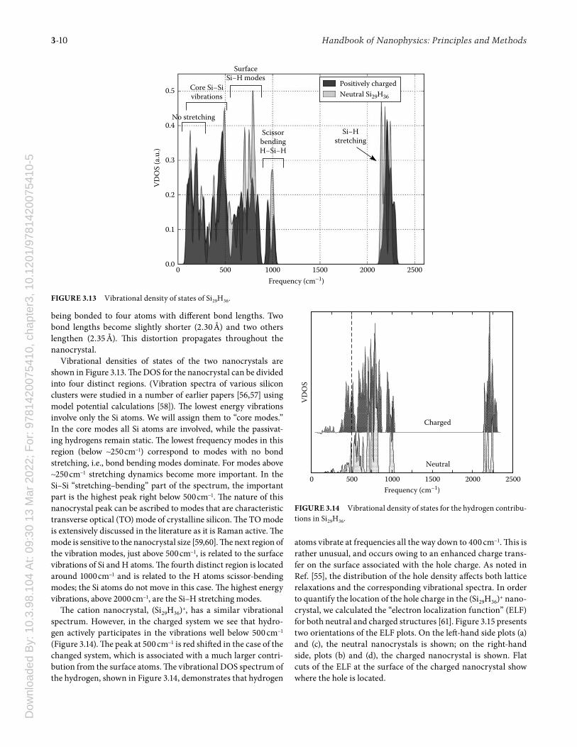
Vibrational densities of states of the two nanocrystals are shown in Figure 3.13. Th e DOS for the nanocrystal can be divided into four distinct regions. (Vibration spectra of various silicon clusters were studied in a number of earlier papers [56,57] using model potential calculations [58]). Th e lowest energy vibrations involve only the Si atoms. We will assign them to “core modes.” In the core modes all Si atoms are involved, while the passivat-ing hydrogens remain static. Th e lowest frequency modes in this region (below ∼250 cm−1) correspond to modes with no bond stretching, i.e., bond bending modes dominate. For modes above ∼250 cm−1 stretching dynamics become more important. In the Si–Si “stretching–bending” part of the spectrum, the important part is the highest peak right below 500 cm−1. Th e nature of this nanocrystal peak can be ascribed to modes that are characteristic transverse optical (TO) mode of crystalline silicon. Th e TO mode is extensively discussed in the literature as it is Raman active. Th e mode is sensitive to the nanocrystal size [59,60]. Th e next region of the vibration modes, just above 500 cm−1, is related to the surface vibrations of Si and H atoms. Th e fourth distinct region is located around 1000 cm−1 and is related to the H atoms scissor-bending modes; the Si atoms do not move in this case. Th e highest energy vibrations, above 2000 cm−1, are the Si–H stretching modes.
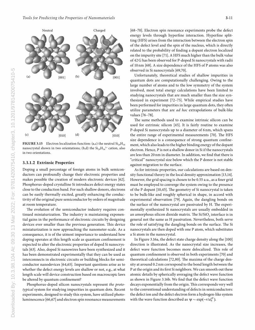
Th e cation nanocrystal, (Si29H36)+, has a similar vibrational spectrum. However, in the charged system we see that hydro-gen actively participates in the vibrations well below 500 cm−1 (Figure 3.14). Th e peak at 500 cm−1 is red shift ed in the case of the changed system, which is associated with a much larger contri-bution from the surface atoms. Th e vibrational DOS spectrum of the hydrogen, shown in Figure 3.14, demonstrates that hydrogen
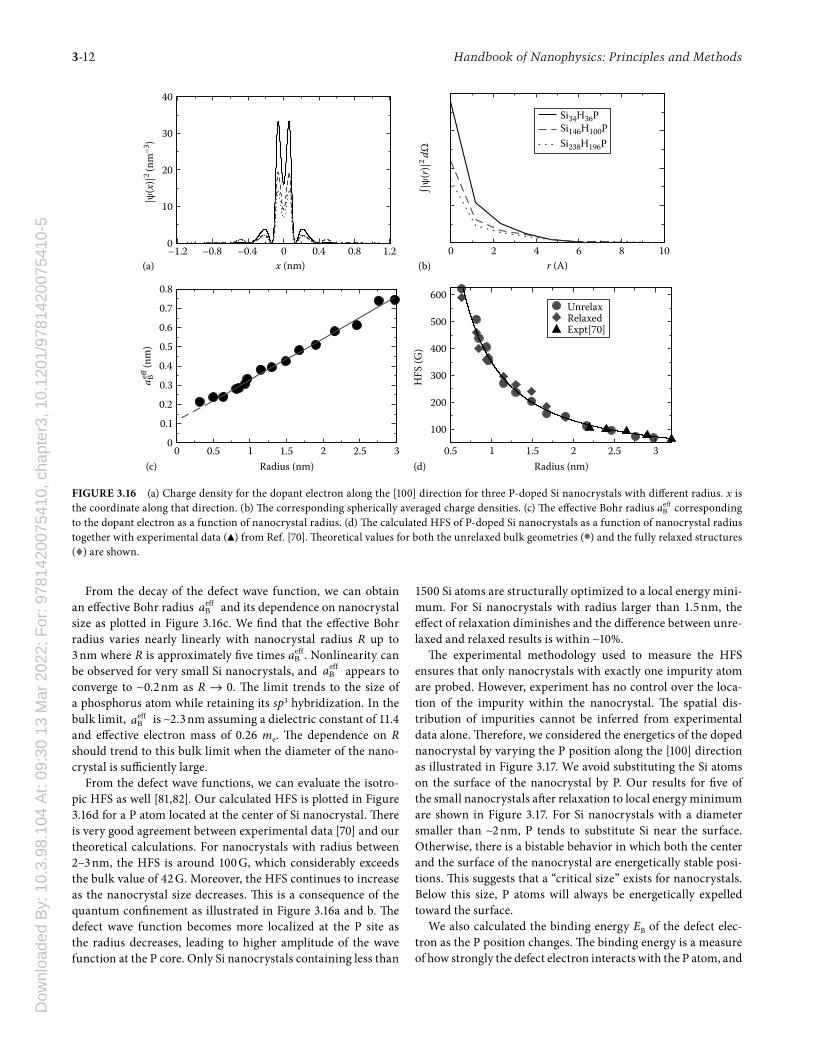
atoms vibrate at frequencies all the way down to 400 cm−1. Th is is rather unusual, and occurs owing to an enhanced charge trans-fer on the surface associated with the hole charge. As noted in Ref. [55], the distribution of the hole density aff ects both lattice relaxations and the corresponding vibrational spectra. In order to quantify the location of the hole charge in the (Si29H36)+ nano-crystal, we calculated the “electron localization function” (ELF) for both neutral and charged structures [61]. Figure 3.15 presents two orientations of the ELF plots. On the left -hand side plots (a) and (c), the neutral nanocrystals is shown; on the right-hand side, plots (b) and (d), the charged nanocrystal is shown. Flat cuts of the ELF at the surface of the charged nanocrystal show where the hole is located.
SurfaceSi−H modes
Si−Hstretching
Core Si−Sivibrations
No stretching
ScissorbendingH−Si−H
0.5
0.4
0.3
0.2
0.1
0.00 500 1000 1500
Frequency (cm–1)
Positively chargedNeutral Si29H36
VD
OS
(a.u
.)
2000 2500
FIGURE 3.13 Vibrational density of states of Si29H36.
0 500 1000 1500 2000 2500Frequency (cm–1)
VD
OS
Charged
Neutral
FIGURE 3.14 Vibrational density of states for the hydrogen contribu-tions in Si29H36.
Dow
nloa
ded
By:
10.
3.98
.104
At:
09:3
0 13
Mar
202
2; F
or: 9
7814
2007
5410
, cha
pter
3, 1
0.12
01/9
7814
2007
5410
-5Tools for Predicting the Properties of Nanomaterials 3-11
3.3.1.2 Extrinsic Properties
Doping a small percentage of foreign atoms in bulk semicon-ductors can profoundly change their electronic properties and makes possible the creation of modern electronic devices [62]. Phosphorus-doped crystalline Si introduces defect energy states close to the conduction band. For such shallow donors, electrons can be easily thermally excited, greatly enhancing the conduc-tivity of the original pure semiconductor by orders of magnitude at room temperature.
Th e evolution of the semiconductor industry requires con-tinued miniaturization. Th e industry is maintaining exponen-tial gains in the performance of electronic circuits by designing devices ever smaller than the previous generation. Th is device miniaturization is now approaching the nanometer-scale. As a consequence, it is of the utmost importance to understand how doping operates at this length scale as quantum confi nement is expected to alter the electronic properties of doped Si nanocrys-tals [63]. Also, doped Si nanowires have been synthesized and it has been demonstrated experimentally that they can be used as interconnects in electronic circuits or building blocks for semi-conductor nanodevices [64,65]. Important questions arise as to whether the defect energy levels are shallow or not, e.g., at what length scale will device construction based on macroscopic laws be altered by quantum confi nement?
Phosphorus-doped silicon nanocrystals represent the proto-typical system for studying impurities in quantum dots. Recent experiments, designed to study this system, have utilized photo-luminescence [66,67] and electron spin resonance measurements
[68–70]. Electron spin resonance experiments probe the defect energy levels through hyperfi ne interaction. Hyperfi ne split-ting (HFS) arises from the interaction between the electron spin of the defect level and the spin of the nucleus, which is directly related to the probability of fi nding a dopant electron localized on the impurity site [71]. A HFS much higher than the bulk value of 42 G has been observed for P-doped Si nanocrystals with radii of 10 nm [68]. A size dependence of the HFS of P atoms was also observed in Si nanocrystals [69,70].
Unfortunately, theoretical studies of shallow impurities in quantum dots are computationally challenging. Owing to the large number of atoms and to the low symmetry of the system involved, most total energy calculations have been limited to studying nanocrystals that are much smaller than the size syn-thesized in experiment [72–75]. While empirical studies have been performed for impurities in large quantum dots, they oft en utilize parameters that are ad hoc extrapolations of bulk-like values [76–78].
Th e same methods used to examine intrinsic silicon can be used for extrinsic silicon [45]. It is fairly routine to examine P-doped Si nanocrystals up to a diameter of 6 nm, which spans the entire range of experimental measurements [70]. Th e HFS size dependence is a consequence of strong quantum confi ne-ment, which also leads to the higher binding energy of the dopant electron. Hence, P is not a shallow donor in Si if the nanocrystals are less than 20 nm in diameter. In addition, we fi nd that there is “critical” nanocrystal size below which the P donor is not stable against migration to the surface.
As for intrinsic properties, our calculations are based on den-sity functional theory in the local density approximation [13,14]. However, the grid spacing is chosen to be 0.55 a.u., as a fi ner grid must be employed to converge the system owing to the presence of the P dopant [10,45]. Th e geometry of Si nanocrystal is taken to be bulk-like and roughly spherical in shape, in accord with experimental observation [79]. Again, the dangling bonds on the surface of the nanocrystal are passivated by H. Th e experi-mentally synthesized Si nanocrystals are usually embedded in an amorphous silicon dioxide matrix. Th e Si/SiO2 interface is in general not the same as H passivation. Nevertheless, both serve the role of satisfying the dangling bonds on the surface. Th e Si nanocrystals are then doped with one P atom, which substitutes a Si atom in the nanocrystal.
In Figure 3.16a, the defect state charge density along the [100] direction is illustrated. As the nanocrystal size increases, the defect wave function becomes more delocalized. Th is role of quantum confi nement is observed in both experiments [70] and theoretical calculations [72,80]. Th e maxima of the charge den-sity at around 0.2 nm correspond to the bond length between the P at the origin and its fi rst Si neighbors. We can smooth out these atomic details by spherically averaging the defect wave function as shown in Figure 3.16b. We fi nd that the defect wave function decays exponentially from the origin. Th is corresponds very well to the conventional understanding of defects in semiconductors: the defect ion and the defect electron form a hydrogen-like system with the wave function described as ( )ψ − eff
Bexp /r a∼ .
Charged
(b) [001]
Neutral
(a) [001]
(d) [010](c) [010]
FIGURE 3.15 Electron localization function: (a,c) the neutral Si29H36 nanocrystal shown in two orientations; (b,d) the Si29H36
1+ cation, also in two orientations.
Dow
nloa
ded
By:
10.
3.98
.104
At:
09:3
0 13
Mar
202
2; F
or: 9
7814
2007
5410
, cha
pter
3, 1
0.12
01/9
7814
2007
5410
-53-12 Handbook of Nanophysics: Principles and Methods
From the decay of the defect wave function, we can obtain an eff ective Bohr radius eff
Ba and its dependence on nanocrystal size as plotted in Figure 3.16c. We fi nd that the eff ective Bohr radius varies nearly linearly with nanocrystal radius R up to 3 nm where R is approximately fi ve times eff
Ba . Nonlinearity can be observed for very small Si nanocrystals, and eff
Ba appears to converge to ∼0.2 nm as R → 0. Th e limit trends to the size of a phosphorus atom while retaining its sp3 hybridization. In the bulk limit, eff
Ba is ∼2.3 nm assuming a dielectric constant of 11.4 and eff ective electron mass of 0.26 me. Th e dependence on R should trend to this bulk limit when the diameter of the nano-crystal is suffi ciently large.
From the defect wave functions, we can evaluate the isotro-pic HFS as well [81,82]. Our calculated HFS is plotted in Figure 3.16d for a P atom located at the center of Si nanocrystal. Th ere is very good agreement between experimental data [70] and our theoretical calculations. For nanocrystals with radius between 2–3 nm, the HFS is around 100 G, which considerably exceeds the bulk value of 42 G. Moreover, the HFS continues to increase as the nanocrystal size decreases. Th is is a consequence of the quantum confi nement as illustrated in Figure 3.16a and b. Th e defect wave function becomes more localized at the P site as the radius decreases, leading to higher amplitude of the wave function at the P core. Only Si nanocrystals containing less than
1500 Si atoms are structurally optimized to a local energy mini-mum. For Si nanocrystals with radius larger than 1.5 nm, the eff ect of relaxation diminishes and the diff erence between unre-laxed and relaxed results is within ∼10%.
Th e experimental methodology used to measure the HFS ensures that only nanocrystals with exactly one impurity atom are probed. However, experiment has no control over the loca-tion of the impurity within the nanocrystal. Th e spatial dis-tribution of impurities cannot be inferred from experimental data alone. Th erefore, we considered the energetics of the doped nanocrystal by varying the P position along the [100] direction as illustrated in Figure 3.17. We avoid substituting the Si atoms on the surface of the nanocrystal by P. Our results for fi ve of the small nanocrystals aft er relaxation to local energy minimum are shown in Figure 3.17. For Si nanocrystals with a diameter smaller than ∼2 nm, P tends to substitute Si near the surface. Otherwise, there is a bistable behavior in which both the center and the surface of the nanocrystal are energetically stable posi-tions. Th is suggests that a “critical size” exists for nanocrystals. Below this size, P atoms will always be energetically expelled toward the surface.
We also calculated the binding energy EB of the defect elec-tron as the P position changes. Th e binding energy is a measure of how strongly the defect electron interacts with the P atom, and
–1.2 –0.8 –0.4 0 0.4 0.8 1.2x (nm)
0
10
20
30
40
|ψ(x
)|2 (n
m–3
)
0 2 4 6 8 10r (A)
∫|ψ(
r)|2
dΩ
Si34H36PSi146H100PSi238H196P
0 0.5 1 1.5 2 2.5 3Radius (nm)
0
0.1
0.2
0.3
0.4
0.5
0.6
0.7
0.8
a Beff (n
m)
0.5 1 1.5 2 2.5 3Radius (nm)
100
200
300
400
500
600
HFS
(G)
UnrelaxRelaxedExpt[70]
(a) (b)
(c) (d)
FIGURE 3.16 (a) Charge density for the dopant electron along the [100] direction for three P-doped Si nanocrystals with diff erent radius. x is the coordinate along that direction. (b) Th e corresponding spherically averaged charge densities. (c) Th e eff ective Bohr radius eff
Ba corresponding to the dopant electron as a function of nanocrystal radius. (d) Th e calculated HFS of P-doped Si nanocrystals as a function of nanocrystal radius together with experimental data (▲) from Ref. [70]. Th eoretical values for both the unrelaxed bulk geometries (•) and the fully relaxed structures (♦) are shown.
Dow
nloa
ded
By:
10.
3.98
.104
At:
09:3
0 13
Mar
202
2; F
or: 9
7814
2007
5410
, cha
pter
3, 1
0.12
01/9
7814
2007
5410
-5Tools for Predicting the Properties of Nanomaterials 3-13
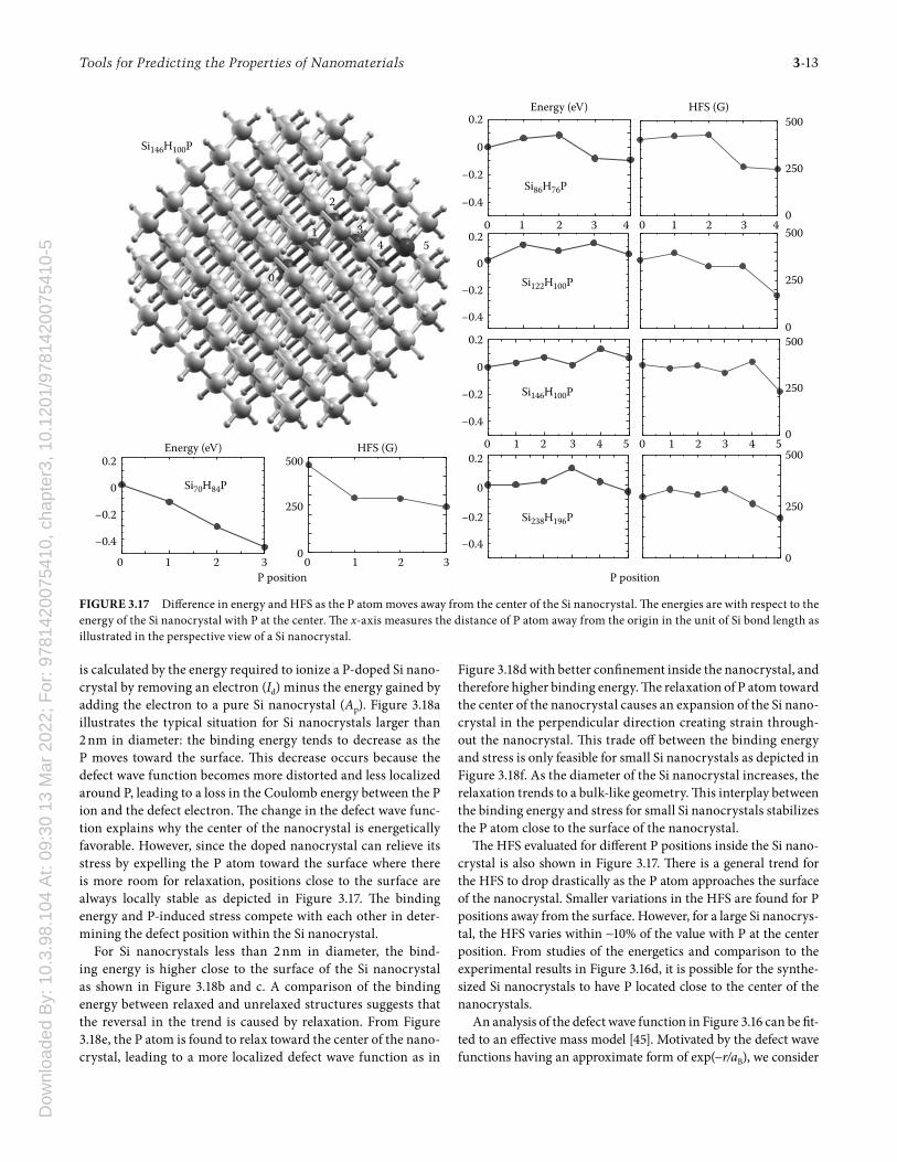
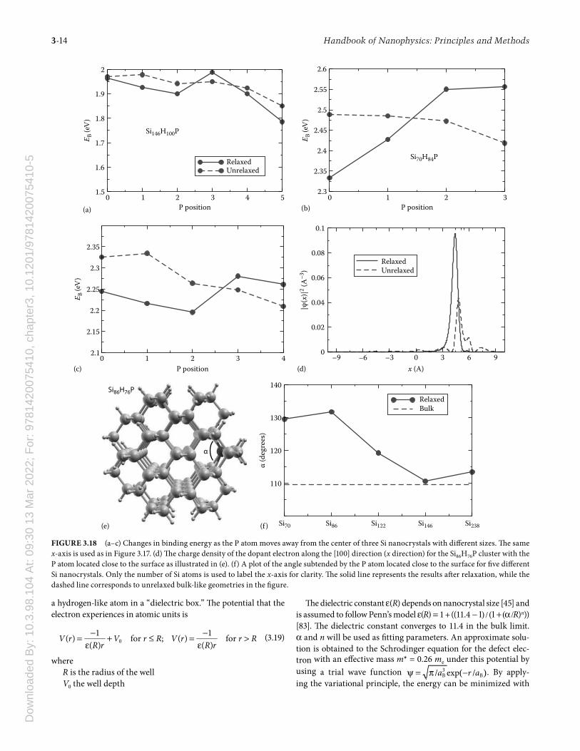
is calculated by the energy required to ionize a P-doped Si nano-crystal by removing an electron (Id) minus the energy gained by adding the electron to a pure Si nanocrystal (Ap). Figure 3.18a illustrates the typical situation for Si nanocrystals larger than 2 nm in diameter: the binding energy tends to decrease as the P moves toward the surface. Th is decrease occurs because the defect wave function becomes more distorted and less localized around P, leading to a loss in the Coulomb energy between the P ion and the defect electron. Th e change in the defect wave func-tion explains why the center of the nanocrystal is energetically favorable. However, since the doped nanocrystal can relieve its stress by expelling the P atom toward the surface where there is more room for relaxation, positions close to the surface are always locally stable as depicted in Figure 3.17. Th e binding energy and P-induced stress compete with each other in deter-mining the defect position within the Si nanocrystal.
For Si nanocrystals less than 2 nm in diameter, the bind-ing energy is higher close to the surface of the Si nanocrystal as shown in Figure 3.18b and c. A comparison of the binding energy between relaxed and unrelaxed structures suggests that the reversal in the trend is caused by relaxation. From Figure 3.18e, the P atom is found to relax toward the center of the nano-crystal, leading to a more localized defect wave function as in
Figure 3.18d with better confi nement inside the nanocrystal, and therefore higher binding energy. Th e relaxation of P atom toward the center of the nanocrystal causes an expansion of the Si nano-crystal in the perpendicular direction creating strain through-out the nanocrystal. Th is trade off between the binding energy and stress is only feasible for small Si nanocrystals as depicted in Figure 3.18f. As the diameter of the Si nanocrystal increases, the relaxation trends to a bulk-like geometry. Th is interplay between the binding energy and stress for small Si nanocrystals stabilizes the P atom close to the surface of the nanocrystal.
Th e HFS evaluated for diff erent P positions inside the Si nano-crystal is also shown in Figure 3.17. Th ere is a general trend for the HFS to drop drastically as the P atom approaches the surface of the nanocrystal. Smaller variations in the HFS are found for P positions away from the surface. However, for a large Si nanocrys-tal, the HFS varies within ∼10% of the value with P at the center position. From studies of the energetics and comparison to the experimental results in Figure 3.16d, it is possible for the synthe-sized Si nanocrystals to have P located close to the center of the nanocrystals.
An analysis of the defect wave function in Figure 3.16 can be fi t-ted to an eff ective mass model [45]. Motivated by the defect wave functions having an approximate form of exp(−r/aB), we consider
2
0
1 34 5
Si86H76P
Si146H100P
Si238H196P
Si122H100P
Si70H84P
Si146H100P
250
HFS (G)
0 41 32
250
0 2 3 41 5
250
250
500
0500
5000
500
0
0
Energy (eV)
43210
543210
0.2
−0.2
−0.4
0
0.2
0
−0.4
−0.2
0.2
0
−0.2
−0.4
0.2
0
−0.2
−0.4
HFS (G)
0
500
250
Energy (eV)0.2
0
−0.2
−0.4
00 31 2 1 2 3P position P position
FIGURE 3.17 Diff erence in energy and HFS as the P atom moves away from the center of the Si nanocrystal. Th e energies are with respect to the energy of the Si nanocrystal with P at the center. Th e x-axis measures the distance of P atom away from the origin in the unit of Si bond length as illustrated in the perspective view of a Si nanocrystal.
Dow
nloa
ded
By:
10.
3.98
.104
At:
09:3
0 13
Mar
202
2; F
or: 9
7814
2007
5410
, cha
pter
3, 1
0.12
01/9
7814
2007
5410
-53-14 Handbook of Nanophysics: Principles and Methods
a hydrogen-like atom in a “dielectric box.” Th e potential that the electron experiences in atomic units is
− −= + ≤ = >ε ε0
1 1( ) for ; ( ) for( ) ( )
V r V r R V r r RR r R r
(3.19)
whereR is the radius of the wellV0 the well depth
Th e dielectric constant ε(R) depends on nanocrystal size [45] and is assumed to follow Penn’s model ε(R) = 1 + ((11.4 − 1) / (1 + (α /R)n)) [83]. Th e dielectric constant converges to 11.4 in the bulk limit. α and n will be used as fi tting parameters. An approximate solu-tion is obtained to the Schrodinger equation for the defect elec-tron with an eff ective mass m* = 0.26 me under this potential by using a trial wave function ( )3
B B/ exp /a r aψ = π − . By apply-ing the variational principle, the energy can be minimized with
0 1 2 3 42.1
2.15
2.2
2.25
2.3
2.35
E B (e
V)
0 1 2 3 4 51.5
1.6
1.7
1.8
1.9
2
E B (e
V)
RelaxedUnrelaxed
Si146H100P
P position(c)
(a) P position0 1 2 3
2.3
2.35
2.4
2.45
2.5
2.55
2.6
E B (e
V)
–9 –6 –3 0 3 6 9x (A)
0
0.02
0.04
0.06
0.08
0.1
|ψ(x
)|2 (A–3
)
RelaxedUnrelaxed
Si70H84P
(b)
(d)
P position
Si70 Si86 Si122 Si146 Si238
110
120
130
140
α (d
egre
es)
RelaxedBulk
(f )
Si86H76P
α
(e)
FIGURE 3.18 (a–c) Changes in binding energy as the P atom moves away from the center of three Si nanocrystals with diff erent sizes. Th e same x-axis is used as in Figure 3.17. (d) Th e charge density of the dopant electron along the [100] direction (x direction) for the Si86H76P cluster with the P atom located close to the surface as illustrated in (e). (f) A plot of the angle subtended by the P atom located close to the surface for fi ve diff erent Si nanocrystals. Only the number of Si atoms is used to label the x-axis for clarity. Th e solid line represents the results aft er relaxation, while the dashed line corresponds to unrelaxed bulk-like geometries in the fi gure.
Dow
nloa
ded
By:
10.
3.98
.104
At:
09:3
0 13
Mar
202
2; F
or: 9
7814
2007
5410
, cha
pter
3, 1
0.12
01/9
7814
2007
5410
-5Tools for Predicting the Properties of Nanomaterials 3-15
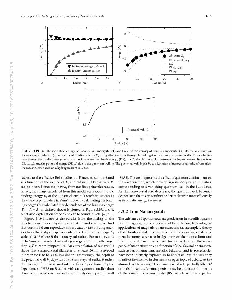
respect to the eff ective Bohr radius aB. Hence, aB can be found as a function of the well depth V0 and radius R. Alternatively, V0 can be inferred since we know aB from our fi rst-principles results. In fact, the energy calculated from this model corresponds to the binding energy EB of the dopant electron. Th erefore, we can fi t the α and n parameters in Penn’s model by calculating the bind-ing energy. Our calculated size dependence of the binding energy (EB = Id − Ap as defi ned above) is plotted in Figure 3.19a and b. A detailed explanation of the trend can be found in Refs. [45,72].
Figure 3.19 illustrates the results from the fitting to the effective mass model. By using α = 5.4 nm and n = 1.6, we fi nd that our model can reproduce almost exactly the binding ener-gies from the fi rst-principles calculations. Th e binding energy EB scales as R−1.1 where R the nanocrystal radius. For nanocrystals up to 6 nm in diameter, the binding energy is signifi cantly larger than kBT at room temperature. An extrapolation of our results shows that a nanocrystal diameter of at least 20 nm is needed in order for P to be a shallow donor. Interestingly, the depth of the potential well V0 depends on the nanocrystal radius R rather than being infi nite or a constant. Th e fi nite V0 explains why the dependence of HFS on R scales with an exponent smaller than three, which is a consequence of an infi nitely deep quantum well
[84,85]. Th e well represents the eff ect of quantum confi nement on the wave function, which for very large nanocrystals diminishes, corresponding to a vanishing quantum well in the bulk limit. As the nanocrystal size decreases, the quantum well becomes deeper such that it can confi ne the defect electron more eff ectively as its kinetic energy increases.
3.3.2 Iron Nanocrystals
Th e existence of spontaneous magnetization in metallic systems is an intriguing problem because of the extensive technological applications of magnetic phenomena and an incomplete theory of its fundamental mechanisms. In this scenario, clusters of metallic atoms serve as a bridge between the atomic limit and the bulk, and can form a basis for understanding the emer-gence of magnetization as a function of size. Several phenomena such as ferromagnetism, metallic behavior, and ferroelectricity have been intensely explored in bulk metals, but the way they manifest themselves in clusters is an open topic of debate. At the atomic level, ferromagnetism is associated with partially fi lled 3d orbitals. In solids, ferromagnetism may be understood in terms of the itinerant electron model [86], which assumes a partial
10 15 20 25 30Radius (A)
–2
–1.5
–1
–0.5
0
Ener
gy (e
V)
Potential well V0
(c)
10 15 20 25 30Radius (A)
–4
–2
0
2
Ener
gy (e
V)
Ab-initio EBEff. mass theoryKEPECoulombPEQW
0.8 1.2 1.6 2 2.4 2.8Radius (nm)
1
2
3
4
5
Ener
gy (e
V)
Ionization energy (P-Si nc)Electron affinity (Si nc)
(a) (b)
FIGURE 3.19 (a) Th e ionization energy of P-doped Si nanocrystal (▼) and the electron affi nity of pure Si nanocrystal (▲) plotted as a function of nanocrystal radius. (b) Th e calculated binding energy EB using eff ective mass theory plotted together with our ab initio results. From eff ective mass theory, the binding energy has contributions from the kinetic energy (KE), the Coulomb interaction between the dopant ion and its electron (PECoulomb), and the potential energy (PEQW) due to the quantum well. (c) Th e potential well depth V0 as a function of nanocrystal radius from eff ec-tive mass theory based on a hydrogen atom in a box.
Dow
nloa
ded
By:
10.
3.98
.104
At:
09:3
0 13
Mar
202
2; F
or: 9
7814
2007
5410
, cha
pter
3, 1
0.12
01/9
7814
2007
5410
-53-16 Handbook of Nanophysics: Principles and Methods
delocalization of the 3d orbitals. In clusters of iron atoms, delo-calization is weaker owing to the presence of a surface, whose shape aff ects the magnetic properties of the cluster. Because of their small size, iron clusters containing a few tens to hundreds of atoms are superparamagnetic: Th e entire cluster serves as a single magnetic domain, with no internal grain boundaries [87]. Consequently, these clusters have strong magnetic moments, but exhibit no hysteresis.
Th e magnetic moment of nano-sized clusters has been mea-sured as a function of temperature and size [88–90], and several aspects of the experiment have not been fully clarifi ed, despite the intense work on the subject [91–96]. One intriguing experi-mental observation is that the specifi c heat of such clusters is lower than the Dulong–Petit value, which may be due to a mag-netic phase transition [89]. In addition, the magnetic moment per atom does not decay monotonically as a function of the number of atoms and for fi xed temperature. Possible explana-tions for this behavior are structural phase transitions, a strong dependence of magnetization with the shape of the cluster, or coupling with vibrational modes [89]. One diffi culty is that the structure of such clusters is not well known. First-principles and model calculations have shown that clusters with up to 10 or 20 atoms assume a variety of exotic shapes in their lowest-energy confi guration [97,98]. For larger clusters, there is indication for a stable body-centered cubic (BCC) structure, which is identical to ferromagnetic bulk iron [91].
Th e evolution of magnetic moment as a function of cluster size has attracted considerable attention from researchers in the fi eld [88–98]. A key question to be resolved is: What drives the sup-pression of magnetic moment as clusters grow in size? In the iron atom, the permanent magnetic moment arises from exchange splitting: the 3d↑ orbitals (majority spin) are low in energy and completely occupied with fi ve electrons, while the 3d↓ orbitals (minority spin) are partially occupied with one electron, result-ing in a magnetic moment of 4 μB, μB being the Bohr magneton. When atoms are assembled in a crystal, atomic orbitals hybrid-ize and form energy bands: 4s orbitals create a wide band that remains partially fi lled, in contrast with the completely fi lled 4s orbital in the atom; while the 3d↓ and 3d↑ orbitals create nar-rower bands. Orbital hybridization together with the diff erent bandwidths of the various 3d and 4s bands result in weaker mag-netization, equivalent to 2.2 μB/atom in bulk iron.
In atomic clusters, orbital hybridization is not as strong because atoms on the surface of the cluster have fewer neigh-bors. Th e strength of hybridization can be quantifi ed by the eff ective coordination number. A theoretical analysis of mag-netization in clusters and thin slabs indicates that the depen-dence of the magnetic moment with the eff ective coordination number is approximately linear [93,95,96]. But the suppression of magnetic moment from orbital hybridization is not isotropic [99]. If we consider a layer of atoms for instance, the 3d orbitals oriented in the plane of atoms will hybridize more eff ectively than orbitals oriented normal to the plane. As a consequence, clusters with faceted surfaces are expected to have magnetic properties diff erent from clusters with irregular surfaces, even
if they have the same eff ective coordination number [99]. Th is eff ect is likely responsible for a nonmonotonic suppression of magnetic moment as a function of cluster size. In order to ana-lyze the role of surface faceting more deeply, we have performed fi rst-principles calculations of the magnetic moment of iron clusters with various geometries and with sizes ranging from 20 to 400 atoms.
Th e Kohn–Sham equation can be applied to this problem using a spin-density functional. We used the generalized gradi-ent approximation (GGA) [100] and the computational details are as outlined elsewhere [8,24,31,101]. Obtaining an accurate description of the electronic and magnetic structures of iron clusters is more diffi cult than for simple metal clusters. Of course, the existence of a magnetic moment means an additional degree of freedom enters the problem. In principle, we could consider non-collinear magnetism and associate a magnetic vec-tor at every point in space. Here we assume a collinear descrip-tion owing to the high symmetry of the clusters considered. In either case, we need to consider a much larger confi guration space for the electronic degrees of freedom. Another issue is the relatively localized nature of the 3d electronic states. For a real space approach, to obtain a fully converged solution, we need to employ a much fi ner grid spacing than for simple metals, typi-cally 0.3 a.u. In contrast, for silicon one might use a spacing of 0.7 a.u. Th is fi ner grid required for iron results in a much larger Hamiltonian matrix and a corresponding increase in the com-putational load. As a consequence, while we can consider nano-crystals of silicon with over 10,000 atoms, nanocrystals of iron of this size are problematic.
Th e geometry of the iron clusters introduces a number of degrees of freedom. It is not currently possible to determine the defi nitive ground state for systems with dozens of atoms as myri-ads of clusters can exist with nearly degenerate energies. However, in most cases, it is not necessary to know the ground state. We are more interested in determining what structures are “reasonable” and representative of the observed ensemble, i.e., if two structures are within a few meV, these structures are not distinguishable.
We considered topologically distinct clusters, e.g., clusters of both icosahedral and BCC symmetry were explored in our work. In order to investigate the role of surface faceting, we constructed clusters with faceted and non-faceted surfaces. Faceted clusters are constructed by adding successive atomic layers around a nucleation point. Small faceted icosahedral clusters exist with sizes 13, 55, 147, and 309. Faceted BCC clusters are constructed with BCC local coordination and, diff erently from icosahedral ones, they do not need to be centered on an atom site.
We consider two families of cubic clusters: atom-centered or bridge-centered, respectively for clusters with nucleation point at an atom site or on the bridge between two neighboring atoms. Th e lattice parameter is equal to the bulk value, 2.87 Å. Non-faceted clusters are built by adding shells of atoms around a nucleation point so that their distance to the nucleation point is less than a specifi ed value. As a result, non-faceted clusters usu-ally have narrow steps over otherwise planar surfaces and the overall shape is almost spherical. By construction, non-faceted

Dow
nloa
ded
By:
10.
3.98
.104
At:
09:3
0 13
Mar
202
2; F
or: 9
7814
2007
5410
, cha
pter
3, 1
0.12
01/9
7814
2007
5410
-5Tools for Predicting the Properties of Nanomaterials 3-17
clusters have well-defi ned point-group symmetries: Ih or Th for the icosahedral family, Oh for the atom-centered family, and D4h for the bridge-centered family. Clusters constructed in that manner show low tension on the surface, making surface recon-struction less likely.
As clusters grow in size, their properties approach the proper-ties of bulk iron. Figure 3.20a shows the DOS for Fe388, with local BCC coordination. At this size range, the DOS assumes a shape typical of bulk iron, with a three-fold partition of the 3d bands. In addition, the cohesive energy of this cluster is only 77 meV lower than in bulk. Th is evidence suggests that interesting size eff ects will be predominantly observed in clusters smaller than Fe388. Figure 3.20b shows the DOS for Fe393, which belongs to the icosahedral family. Th is cluster has a very smooth DOS, with not much structure compared to Fe388 and bulk BCC iron. Th is is due to the icosahedral-like arrangement of atoms in Fe393. Th e overall dispersion of the 3d peak (4 eV for 3d↑ and 6 eV for 3d↓) is nevertheless similar in all the calculated DOS.
Th e magnetic moment is calculated as the expectation value of the total angular momentum:
BB
1( )2
ss z z z
gM g S L n n L↑ ↓μ ⎡ ⎤⎡ ⎤= + = μ − +⎢ ⎥⎣ ⎦ ⎣ ⎦� �
(3.20)
where gs = 2 is the electron gyromagnetic ratio. Figure 3.21 illustrates the approximately linear dependence between the magnetic moment and the spin moment, <Sz>, throughout the whole size range. Th is results in an eff ective gyromagnetic ratio geff = 2.04 μB/ћ, which is somewhat smaller than the gyromag-netic ratio in bulk BCC iron, 2.09 μB/ћ. Th is is probably due to an underestimation in the orbital contribution, <Lz>. In the absence of an external magnetic fi eld, orbital magnetization arises from the spin-orbit interaction, which is included in the theory as a model potential,
soV = −ξ ⋅L S (3.21)
where ξ = 80 meV/ћ2 [93].
Figure 3.22 shows the magnetic moment of several clusters belonging to the three families studied: atom-centered BCC (top panel), bridge-centered BCC (middle panel), and icosahe-dral (bottom panel). Experimental data obtained by Billas and collaborators [88] are also shown. Th e suppression of magnetic moment as a function of size is readily observed. Also, clusters with faceted surfaces are predicted to have magnetic moments lower than other clusters with similar sizes. Th is is attributed to the more eff ective hybridization of d orbitals along the plane of the facets.
Th e non-monotonic behavior of the measured magnetic moment with size cluster can be attributed to the shape of the surface. Under this assumption, islands of low magnetic moment (observed at sizes 45, 85, and 188) are associated to clusters with faceted surfaces. In the icosahedral family, the islands of low magnetic moment are located around faceted clusters contain-ing 55, 147, and 309 atoms. Th e fi rst island is displaced by 10 units from the measured location. For the atom-centered and bridge-centered families, we found islands at (65, 175) and (92, 173) respectively, as indicated in Figure 3.22a and b. Th e fi rst
0
1
2
–8 –4 0 4Energy – EFermi (eV)(a)
1
2
Den
sity o
f sta
tes (
eV–1
)Majority spin
Minority spin
Fe388
0
1
2
–8 –4 0 4Energy – EFermi (eV)(b)
1
2
Den
sity o
f sta
tes (
eV–1
)
Majority spin
Minority spin
Fe393
FIGURE 3.20 Density of states in the clusters Fe388 (a) and Fe393 (b), majority spin (upper panel), and minority spin(lower panel). For reference, the density of states in bulk iron is shown in dashed lines. Th e Fermi energy is chosen as energy reference.
1.32.6
2.8
3
1.4Spin moment (ћ/atom)
Atom centeredBridge centered
Mag
netic
mom
ent (
μ B/a
tom
)
1.5
FIGURE 3.21 Magnetic moment versus spin moment calculated for the atom-centered BCC (“plus” signs) and bridge-centered BCC (crosses) iron clusters. Th e approximate ratio is M/<Sz> = geff = 2.04 μB/ћ.
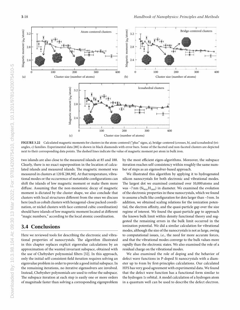
Dow
nloa
ded
By:
10.
3.98
.104
At:
09:3
0 13
Mar
202
2; F
or: 9
7814
2007
5410
, cha
pter
3, 1
0.12
01/9
7814
2007
5410
-53-18 Handbook of Nanophysics: Principles and Methods
two islands are also close to the measured islands at 85 and 188. Clearly, there is no exact superposition in the location of calcu-lated islands and measured islands. Th e magnetic moment was measured in clusters at 120 K [88,90]. At that temperature, vibra-tional modes or the occurrence of metastable confi gurations can shift the islands of low magnetic moment or make them more diff use. Assuming that the non-monotonic decay of magnetic moment is dictated by the cluster shape, we also conclude that clusters with local structures diff erent from the ones we discuss here (such as cobalt clusters with hexagonal-close packed coordi-nation, or nickel clusters with face-centered cubic coordination) should have islands of low magnetic moment located at diff erent “magic numbers,” according to the local atomic coordination.
3.4 Conclusions
Here we reviewed tools for describing the electronic and vibra-tional properties of nanocrystals. Th e algorithm illustrated in this chapter replaces explicit eigenvalue calculations by an approximation of the wanted invariant subspace, obtained with the use of Chebyshev polynomial fi lters [32]. In this approach, only the initial self-consistent-fi eld iteration requires solving an eigenvalue problem in order to provide a good initial subspace. In the remaining iterations, no iterative eigensolvers are involved. Instead, Chebyshev polynomials are used to refi ne the subspace. Th e subspace iteration at each step is easily one or more orders of magnitude faster than solving a corresponding eigenproblem
by the most effi cient eigen-algorithms. Moreover, the subspace iteration reaches self-consistency within roughly the same num-ber of steps as an eigensolver-based approach.
We illustrated this algorithm by applying it to hydrogenated silicon nanocrystals for both electronic and vibrational modes. Th e largest dot we examined contained over 10,000 atoms and was ∼7 nm (Si9041H1860) in diameter. We examined the evolution of the electronic properties in these nanocrystals, which we found to assume a bulk-like confi guration for dots larger than ∼5 nm. In addition, we obtained scaling relations for the ionization poten-tial, the electron affi nity, and the quasi-particle gap over the size regime of interest. We found the quasi-particle gap to approach the known bulk limit within density functional theory and sug-gested the remaining errors in the bulk limit occurred in the ionization potential. We did a similar calculation for vibrational modes, although the size of the nanocrystals is not as large, owing to computational issues, i.e., the need for more accurate forces, and that the vibrational modes converge to the bulk values more rapidly than the electronic states. We also examined the role of a residual charge on the vibrational modes.
We also examined the role of doping and the behavior of defect wave functions in P-doped Si nanocrystals with a diam-eter up to 6 nm by fi rst-principles calculations. Our calculated HFS has very good agreement with experimental data. We found that the defect wave function has a functional form similar to the hydrogen 1s orbital. A model calculation of a hydrogen atom in a quantum well can be used to describe the defect electron.
3.2
2.8
2.4
0(a)
100 200 300
Atom-centered clusters
400 0(b)
2.4
2.8
3.2
100 200
Bridge-centered clusters
Mag
netic
mom
ent (
μ B/a
tom
)
Mag
netic
mom
ent (
μ B/a
tom
)
Mag
netic
mom
ent (
μ B/a
tom
)300 400
0
2.4
2.8
3.2
100 200Cluster size (number of atoms)
Cluster size (number of atoms) Cluster size (number of atoms)
(c)
Icosahedral clusters
300 400
FIGURE 3.22 Calculated magnetic moments for clusters in the atom-centered (“plus” signs, a), bridge-centered (crosses, b), and icosahedral (tri-angles, c) families. Experimental data [88] is shown in black diamonds with error bars. Some of the faceted and non-faceted clusters are depicted next to their corresponding data points. Th e dashed lines indicate the value of magnetic moment per atom in bulk iron.
Dow
nloa
ded
By:
10.
3.98
.104
At:
09:3
0 13
Mar
202
2; F
or: 9
7814
2007
5410
, cha
pter
3, 1
0.12
01/9
7814
2007
5410
-5Tools for Predicting the Properties of Nanomaterials 3-19
In addition, our study on the energetics of P location in the Si nanocrystals indicates that the P atom will be expelled toward the surface of the nanocrystal with diameter below a critical value of ∼2 nm.
Th e computational tools we outlined in this chapter are not restricted to insulating materials as is oft en done in computational methods targeted at large systems [102]. Th e fi ltering method we employ can equally well be applied to metallic systems and we have done so for liquid Pb [43] and for iron nanocrystals [8]. We reviewed our results for the nanocrystals of iron by examining the evolution of the magnetic moment in iron clusters contain-ing 20 to 400 atoms using our real space pseudopotential method with damped Chebyshev fi ltering. Th ree families of clusters were studied. Th ey were characterized by the arrangement of atoms: icosahedral, BCC centered on an atom site, and BCC centered on the bridge between two neighboring atoms. We found an overall decrease of magnetic moment as the clusters grow in size toward the bulk limit. Clusters with faceted surfaces are predicted to have magnetic moment lower than other clusters with similar size. As a result, the magnetic moments is observed to decrease as a func-tion of size in a nonmonotonic manner, which explains measure-ments performed at low temperature.
Th e utility of this numerical approach should be widely applied to a variety of problems at the nanoscale. Th e method is suffi ciently powerful that it can be applied to systems suffi ciently large that the entire nano-regime can be examined from an iso-lated atom to a bulk crystal. Moreover, the method has recently been extended to include systems with partial periodicity, e.g., nanowires where the system is periodic along the axis of the nanowire [35,103].
Acknowledgments
Th is work was supported in part by the National Science Foundation under DMR-0551195 and by the U.S. Department of Energy under DE-FG02-06ER46286 and DE-FG02-06ER15760. Computational support is acknowledged from the Texas Advanced Computing Center (TACC) and the DOE National Energy Research Scientifi c Computing Center (NERSC).
References
1. L. Brus, J. Phys. Chem. 98, 3575 (1994). 2. A. P. Alivisatos, Science 271, 933 (1996). 3. A. P. Alivisatos, J. Phys. Chem. 100, 13226 (1996). 4. X. G. Peng, L. Manna, W. D. Yang, J. Wickham, E. Scher,
A. Kadavanich, and A. P. Alivisatos, Nature 404, 59 (2000). 5. M. Law, J. Goldberger, and P. Yang, Ann. Rev. Mater. Res. 34,
83 (2004). 6. C. Burda, X. B. Chen, R. Narayanan, and M. A. El-Sayed,
Chem. Rev. 105, 1025 (2005). 7. R. Walters, G. Bourianoff , and H. Atwater, Nat. Mater. 4,
143 (2005). 8. M. Tiago, Y. Zhou, M. M. G. Alemany, Y. Saad,
and J. R. Chelikowsky, Phys. Rev. Lett. 97, 147201 (2006).
9. G. Rollmann, M. E. Gruner, A. Hucht, P. Entel, M. L. Tiago, and J. R. Chelikowsky, Phys. Rev. Lett. 99, 083402 (2007).
10. J. R. Chelikowsky, J. Phys. D: Appl. Phys. 33, R33 (2000). 11. L. W. Wang and A. Zunger, J. Chem. Phys. 100, 2394 (1994). 12. L. W. Wang and A. Zunger, J. Phys. Chem. 98, 2158 (1994). 13. W. Kohn and L. J. Sham, Phys. Rev. 140, A1133 (1965). 14. P. Hohenberg and W. Kohn, Phys. Rev. 136, B864 (1964). 15. D. M. Ceperley and B. J. Alder, Phys. Rev. Lett. 45, 566
(1980). 16. C. G. Broyden, Math. Comp. 19, 577 (1965), ISSN 00255718,
URL http://www.jstor. org/stable/2003941. 17. J. R. Chelikowsky and M. L. Cohen, in Handbook of
Semiconductors, edited by T. S. Moss and P. T. Landsberg (Elsevier, Amsterdam, the Netherlands, 1992), p. 59.
18. M. L. Cohen and J. R. Chelikowsky, Electronic Structure and Optical Properties of Semiconductors, 2nd edn. (Springer-Verlag, Berlin, Germany, 1989).
19. D. R. Hamann, M. Schlüter, and C. Chiang, Phys. Rev. Lett. 43, 1494 (1979).
20. G. P. Kerker, J. Phys. C 13, L189 (1980). 21. N. Troullier and J. Martins, Phys. Rev. B 43, 1993 (1991). 22. G. Bachelet, D. R. Hamann, and M. Schlüter, Phys. Rev. B
26, 4199 (1982). 23. G. Kresse and J. Furthmüller, Phys. Rev. B 54, 11169
(1996). 24. J. R. Chelikowsky, N. Troullier, and Y. Saad, Phys. Rev. Lett.
72, 1240 (1994). 25. E. L. Briggs, D. J. Sullivan, and J. Bernholc, Phys. Rev. B 52,
R5471 (1995). 26. G. Zumbach, N. A. Modine, and E. Kaxiras, Solid State
Commun. 99, 57 (1996). 27. J.-L. Fattebert and J. Bernholc, Phys. Rev. B 62, 1713 (2000). 28. T. L. Beck, Rev. Mod. Phys. 74, 1041 (2000). 29. M. Heikanen, T. Torsti, M. J. Puska, and R. M. Nieminen,
Phys. Rev. B 63, 245106 (2001). 30. T. Torsti, T. Eirola, J. Enkovaara, T. Hakala, P. Havu, V. Havu,
T. Höynälänmaa, J. Ignatius, M. Lyly, I. Makkonen et al., Physica Status Solidi (b) 243, 1016 (2006).
31. L. Kronik, A. Makmal, M. L. Tiago, M. M. G. Alemany, M. Jain, X. Huang, Y. Saad, and J. R. Chelikowsky, Physica Status Solidi (b) 243, 1063 (2006).
32. Y. Zhou, Y. Saad, M. L. Tiago, and J. R. Chelikowsky, Phys. Rev. E 74, 066704 (2006).
33. M. M. G. Alemany, M. Jain, J. R. Chelikowsky, and L. Kronik, Phys. Rev. B 69, 075101 (2004).
34. M. Alemany, M. Jain, M. L. Tiago, Y. Zhou, Y. Saad, and J. R. Chelikowsky, Comp. Phys. Commun. 177, 339 (2007).
35. A. Natan, A. Mor, D. Naveh, L. Kronik, M. L. Tiago, S. P. Beckman, and J. R. Chelikowsky, Phys. Rev. B 78, 075109 (2008).
36. B. Fornberg and D. M. Sloan, Acta Numerica 94, 203 (1994).
37. L. Kleinman and D. M. Bylander, Phys. Rev. Lett. 48, 1425 (1982).
38. J. C. Phillips and L. Kleinman, Phys. Rev. 116, 287 (1959).
Dow
nloa
ded
By:
10.
3.98
.104
At:
09:3
0 13
Mar
202
2; F
or: 9
7814
2007
5410
, cha
pter
3, 1
0.12
01/9
7814
2007
5410
-53-20 Handbook of Nanophysics: Principles and Methods
39. A. Stathopoulos, S. Öğüt, Y. Saad, J. Chelikowsky, and H. Kim, Comput. Sci. Eng. 2, 19 (2000).
40. C. Bekas, Y. Saad, M. L. Tiago, and J. R. Chelikowsky, Comp. Phys. Commun. 171, 175 (2005).
41. R. Lehoucq, D. C. Sorensen, and C. Yang, ARPACK Users’ Guide: Solution of Large Scale Eigenvalue Problems by Implicitly Restarted Arnoldi Methods (SIAM, Philadelphia, PA, 1998).
42. K. Wu, A. Canning, H. D. Simon, and L.-W. Wang, J. Comp. Phys. 154, 156 (1999).
43. M. M. G. Alemany, R. C. Longo, L. J. Gallego, D. J. González, L. E. González, M. L. Tiago, and J. R. Chelikowsky, Phys. Rev. B 76, 214203 (2007).
44. S. Furukawa and T. Miyasato, Phys. Rev. B 38, 5726 (1988). 45. T.-L. Chan, M. L. Tiago, E. Kaxiras, and J. R. Chelikowsky,
Nano Lett. 8, 596 (2008). 46. S. Ogut, J. R. Chelikowsky, and S. G. Louie, Phys. Rev. Lett.
79, 1770 (1997). 47. J. P. Perdew and M. Levy, Phys. Rev. Lett. 51, 1884 (1983). 48. L. J. Sham and M. Schlüter, Phys. Rev. Lett. 51, 1888 (1983). 49. M. L. Tiago and J. R. Chelikowsky, Phys. Rev. B 73, 205334
(2006). 50. M. S. Hybertsen and S. G. Louie, Phys. Rev. B 34, 5390
(1986). 51. M. S. Hybertsen and S. G. Louie, Phys. Rev. B 35, 5585 (1987). 52. K. Parlinski, Z. Q. Li, and Y. Kawazoe, Phys. Rev. Lett. 78,
4063 (1997). 53. A. V. Postnikov, O. Pages, and J. Hugel, Phys. Rev. B 71,
115206 (2005). 54. X. Huang, E. Lindgren, and J. R. Chelikowsky, Phys. Rev. B
71, 165328 (2005). 55. J. Song, S. E. Ulloa, and D. A. Drabold, Phys. Rev. B 53, 8042
(1996). 56. X. Jing, N. Troullier, J. R. Chelikowsky, K. Wu, and Y. Saad,
Solid State Commun. 96, 231 (1995). 57. M. R. Pederson, K. Jackson, D. V. Porezag, Z. Hajnal, and
T. Frauenheim, Phys. Rev. B 65, 2863 (1996). 58. A. Valentin, J. Sée, S. Galdin-Retailleau, and P. Dollfus,
J. Phys. 92, 1 (2007). 59. C. Meier, S. Lüttjohann, V. G. Kravets, H. Nienhaus, A. Lorke,
and H. Wiggers, Physica E 32, 155 (2006). 60. X .-S. Zhao, Y.-R. Ge, and X. Zhao, J. Mater. Sci. 33, 4267 (1998). 61. B. Silvi and A. Savin, Nature 371, 683 (1994). 62. B. G. Streetman and S. Banerjee, Solid State Electronic
Devices, 5th edn. (Prentice Hall, Englewood Cliff s, NJ, 2000).
63. A. D. Yoff e, Adv. Phys. 50, 1 (2001). 64. Y. Cui and C. M. Lieber, Science 291, 851 (2001). 65. D. Appell, Nature 419, 553 (2002). 66. A. Mimura, M. Fujii, S. Hayashi, D. Kovalev, and F. Koch,
Phys. Rev. B 62, 12625 (2000). 67. G. Mauckner, W. Rebitzer, K. Th onke, and R. Sauer, Physica
Status Solidi (b) 215, 871 (1999). 68. J. Müller, F. Finger, R. Carius, and H. Wagner, Phys. Rev. B
60, 11666 (1999).
69. B. J. Pawlak, T. Gregorkiewicz, C. A. J. Ammerlaan, and P. F. A. Alkemade, Phys. Rev. B 64, 115308 (2001).
70. M. Fujii, A. Mimura, S. Hayashhi, Y. Yamamoto, and K. Murakami, Phys. Rev. Lett. 89, 206805 (2002).
71. G. Feher, Phys. Rev. 114, 1219 (1959). 72. D. Melnikov and J. R. Chelikowsky, Phys. Rev. Lett. 92,
046802 (2004). 73. Z. Zhou, M. L. Steigerwald, R. A. Friesner, L. Brus, and
M. S. Hybertsen, Phys. Rev. B 71, 245308 (2005). 74. G. Cantele, E. Degoli, E. Luppi, R. Magri, D. Ninno, G. Iadonisi,
and S. Ossicini, Phys. Rev. B 72, 113303 (2005). 75. S. Ossicini, E. Degoli, F. Iori, E. Luppi, R. Magri, G. Cantele,
F. Trani, and D. Ninno, Appl. Phys. Lett. 87, 173120 (2005). 76. C. Y. Fong, H. Zhong, B. M. Klein, and J. S. Nelson, Phys.
Rev. B 49, 7466 (1994). 77. I. H. Lee, K. H. Ahn, Y. H. Kim, R. M. Martin, and
J. P. Leburton, Phys. Rev. B 60, 13720 (1999). 78. M. Lannoo, C. Delerue, and G. Allan, Phys. Rev. Lett. 74,
3415 (1995). 79. M. Fujii, K. Toshikiyo, Y. Takase, Y. Yamaguchi, and S. Hayashi,
J. Appl. Phys. 94, 1990 (2003). 80. G. Allan, C. Delerue, M. Lannoo, and E. Martin, Phys. Rev.
B 52, 11982 (1995). 81. J. A. Weil and J. R. Bolton, Electron Paramagnetic Resonance:
Elementary Th eory and Practical Applications, 2nd edn. (Wiley, Hoboken NJ, 2007).
82. C. G. V. de Walle and P. E. Blöchl, Phys. Rev. B 47, 4244 (1993).
83. D. R. Penn, Phys. Rev. B 128, 2093 (1962). 84. L. E. Brus, J. Chem. Phys. 79, 4403 (1983). 85. L. E. Brus, J. Chem. Phys. 79, 5566 (1983). 86. D. Mattis, Th e Th eory of Magnetism, 2nd edn. (Springer-
Verlag, Berlin, Germany, 1988). 87. C. Bean and J. Livingston, J. Appl. Phys. 30, 120s (1959). 88. I. Billas, J. Becker, A. Châtelain, and W. de Heer, Phys. Rev.
Lett. 71, 4067 (1993). 89. D. Gerion, A. Hirt, I. Billas, A. Châtelain, and W. de Heer,
Phys. Rev. B 62, 7491 (2000). 90. I. Billas, A. Châtelain, and W. de Heer, Science 265, 1682
(1994). 91. J. Franco, A. Vega, and F. Aguilera-Granja, Phys. Rev. B 60,
434 (1999). 92. A. Postnikov and P. Entel, Phase Transitions 77, 149
(2004). 93. O. Šipr, M. Košuth, and H. Ebert, Phys. Rev. B 70, 174423
(2004). 94. A. Postnikov, P. Entel, and J. Soler, Eur. Phys. J. D 25, 261
(2003). 95. R. Félix-Medina, J. Dorantes-Dávila, and G. Pastor, Phys.
Rev. B 67, 094430 (2003). 96. K. Edmonds, C. Binns, S. Baker, S. Thornton, C. Norris,
J. Goedkoop, M. Finazzi, and N. Brookes, Phys. Rev. B 60, 472 (1999).
97. G. Pastor, J. Dorantes-Dávila, and K. Bennemann, Phys. Rev. B 40, 7642 (1989).
Dow
nloa
ded
By:
10.
3.98
.104
At:
09:3
0 13
Mar
202
2; F
or: 9
7814
2007
5410
, cha
pter
3, 1
0.12
01/9
7814
2007
5410
-5Tools for Predicting the Properties of Nanomaterials 3-21
98. O. Diéguez, M. Alemany, C. Rey, P. Ordejón, and L. Gallego, Phys. Rev. B 63, 205407 (2001).
99. P. Bruno, in Magnetismus von Festkörpern und grenzfl ächen, edited by P. Dederichs, P. Grünberg, and W. Zinn (IFF-Ferienkurs, Forschungszentrum Jülich, Germany, 1993), pp. 24.1–24.27.
100. J. P. Perdew, K. Burke, and Y. Wang, Phys. Rev. B 54, 16533 (1996).
101. J. R. Chelikowsky, N. Troullier, K. Wu, and Y. Saad, Phys. Rev. B 50, 11355 (1994).
102. M. J. Gillan, D. R. Bower, A. S. Torralba, and T. Miyazaki, Comp. Phys. Commun. 177, 14 (2007).
103. J. Han, M. L. Tiago, T.-L. Chan, and J. R. Chelikowsky, J. Chem. Phys. 129, 144109 (2008).
104. U. Itoh, Y. Toyoshima, H. Onuki, N. Washida, and T. Ibuki, J. Chem. Phys. 85, 4867 (1986).


![[Sattler K.D. (Ed.)] Handbook of Nanophysics Nano(BookFi.org)](https://img.pdfslide.us/doc/110x75/55cf98ca550346d03399aebe/sattler-kd-ed-handbook-of-nanophysics-nanobookfiorg.jpg)