Embed Size (px)
Citation preview

1. General description
The SC16C550B is a Universal Asynchronous Receiver and Transmitter (UART) used for serial data communications. Its principal function is to convert parallel data into serial data, and vice versa. The UART can handle serial data rates up to 3 Mbit/s.
The SC16C550B is pin compatible with the ST16C550, TL16C550 and PC16C550, and it will power-up to be functionally equivalent to the 16C450. The SC16C550B also provides DMA mode data transfers through FIFO trigger levels and the TXRDY and RXRDY signals (TXRDY and RXRDY are not supported in the HVQFN32 package). On-board status registers provide the user with error indications, operational status, and modem interface control. System interrupts may be tailored to meet user requirements. An internal loopback capability allows on-board diagnostics.
The SC16C550B operates at 5 V, 3.3 V and 2.5 V, and the Industrial temperature range, and is available in plastic HVQFN32, DIP40, PLCC44 and LQFP48 packages.
2. Features and benefits
5 V, 3.3 V and 2.5 V operation
Industrial temperature range
After reset, all registers are identical to the typical 16C450 register set
Capable of running with all existing generic 16C450 software
Pin compatibility with the industry-standard ST16C450/550, TL16C450/550, PC16C450/550
Up to 3 Mbit/s transmit/receive operation at 5 V, 2 Mbit/s at 3.3 V, and 1 Mbit/s at 2.5 V
5 V tolerant on input only pins1
16 byte transmit FIFO
16 byte receive FIFO with error flags
Programmable auto-RTS and auto-CTS
In auto-CTS mode, CTS controls transmitter
In auto-RTS mode, RX FIFO contents and threshold control RTS
Automatic hardware flow control
Software selectable baud rate generator
Four selectable Receive FIFO interrupt trigger levels
Standard modem interface
Standard asynchronous error and framing bits (Start, Stop, and Parity Overrun Break)
Independent receiver clock input
Transmit, Receive, Line Status, and Data Set interrupts independently controlled
SC16C550B5 V, 3.3 V and 2.5 V UART with 16-byte FIFOsRev. 6 — 16 December 2014 Product data sheet
1. For data bus pins D7 to D0, see Table 24 “Limiting values”.

NXP Semiconductors SC16C550B5 V, 3.3 V and 2.5 V UART with 16-byte FIFOs
Fully programmable character formatting:
5, 6, 7, or 8-bit characters
Even, odd, or no-parity formats
1, 11⁄2, or 2-stop bit
Baud generation (up to 3 Mbit/s)
False start-bit detection
Complete status reporting capabilities
3-state output TTL drive capabilities for bidirectional data bus and control bus
Line break generation and detection
Internal diagnostic capabilities:
Loopback controls for communications link fault isolation
Prioritized interrupt system controls
Modem control functions (CTS, RI, DCD, DSR, DTR, RTS)
3. Ordering information
Table 1. Ordering informationIndustrial: VDD = 2.5 V, 3.3 V or 5 V 10 %; Tamb = 40 C to +85 C.
Type number Package
Name Description Version
SC16C550BIA44 PLCC44 plastic leaded chip carrier; 44 leads SOT187-2
SC16C550BIBS HVQFN32 plastic thermal enhanced very thin quad flat package; no leads; 32 terminals; body 5 5 0.85 mm
SOT617-1
SC16C550BIB48 LQFP48 plastic low profile quad flat package; 48 leads; body 7 7 1.4 mm SOT313-2
SC16C550BIN40 DIP40 plastic dual in-line package; 40 leads (600 mil) SOT129-1
SC16C550B All information provided in this document is subject to legal disclaimers. © NXP Semiconductors N.V. 2014. All rights reserved.
Product data sheet Rev. 6 — 16 December 2014 2 of 49
NXP Semiconductors SC16C550B5 V, 3.3 V and 2.5 V UART with 16-byte FIFOs
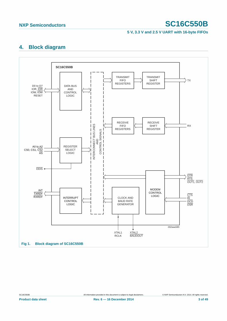
4. Block diagram
Fig 1. Block diagram of SC16C550B
DTRRTSOUT1, OUT2
TRANSMITFIFO
REGISTERSTX
RECEIVESHIFT
REGISTER
RECEIVEFIFO
REGISTERSRX
INT
ER
CO
NN
EC
T B
US
LIN
ES
AN
DC
ON
TR
OL
SIG
NA
LS
SC16C550B
TRANSMITSHIFT
REGISTER
XTAL2BAUDOUT
XTAL1RCLK
002aaa585
DDIS
DATA BUSAND
CONTROLLOGIC
REGISTERSELECTLOGIC
INTERRUPTCONTROL
LOGIC
D0 to D7IOR, IOR
IOW, IOWRESET
A0 to A2CS0, CS1, CS2
AS
INTTXRDYRXRDY CLOCK AND
BAUD RATEGENERATOR
MODEMCONTROL
LOGIC CTSRIDCDDSR
SC16C550B All information provided in this document is subject to legal disclaimers. © NXP Semiconductors N.V. 2014. All rights reserved.
Product data sheet Rev. 6 — 16 December 2014 3 of 49

NXP Semiconductors SC16C550B5 V, 3.3 V and 2.5 V UART with 16-byte FIFOs
5. Pinning information
5.1 Pinning
Fig 2. Pin configuration for PLCC44
Fig 3. Pin configuration for HVQFN32
SC16C550BIA44
D5 RESET
D6 OUT1
D7 DTR
RCLK RTS
RX OUT2
n.c. n.c.
TX INT
CS0 RXRDY
CS1 A0
CS2 A1
BAUDOUT A2
XT
AL1
D4
XT
AL2
D3
IOW
D2
IOW
D1
VS
SD
0
n.c.
n.c.
IOR
VD
D
IOR
RI
DD
ISD
CD
TX
RD
YD
SR
AS
CT
S
002aaa582
7
8
9
10
11
12
13
14
15
16
17
39
38
37
36
35
34
33
32
31
30
29
18 19 20 21 22 23 24 25 26 27 28
6 5 4 3 2 1 44 43 42 41 40
002aab556
SC16C550BIBS
Transparent top view
A2
TX
CS
A1
RX A0
D7 INT
D6 RTS
D5 DTR
n.c. RESET
D4 CTS
VS
S
XT
AL1
XT
AL2
IOW
VS
S
IOR
n.c.
n.c.
D3
D2
D1
D0
VD
D
RI
DC
D
DS
R
8 17
7 18
6 19
5 20
4 21
3 22
2 23
1 24
9 10 11 12 13 14 15 16
32 31 30 29 28 27 26 25
terminal 1index area
SC16C550B All information provided in this document is subject to legal disclaimers. © NXP Semiconductors N.V. 2014. All rights reserved.
Product data sheet Rev. 6 — 16 December 2014 4 of 49
NXP Semiconductors SC16C550B5 V, 3.3 V and 2.5 V UART with 16-byte FIFOs
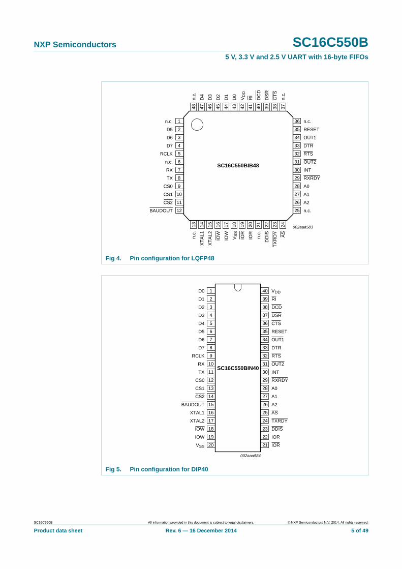
Fig 4. Pin configuration for LQFP48
Fig 5. Pin configuration for DIP40
XT
AL1
XT
AL2
IOW
IOW
VS
S
IOR
IOR
DD
IS
TX
RD
Y
AS
RESET
OUT1
DTR
RTS
OUT2
n.c.
INT
RXRDY
A0
A1
A2
RI
DC
D
DS
R
CT
S
D4
D3
D2
D1
D0
VD
D
D5
D6
D7
RCLK
n.c.
RX
TX
CS0
CS1
CS2
BAUDOUT
SC16C550BIB48
n.c. n.c.
n.c.
n.c.
n.c.
002aaa583
1
2
3
4
5
6
7
8
9
10
11
12
36
35
34
33
32
31
30
29
28
27
26
25
13 14 15 16 17 18 19 20 21 22 23
48 47 46 45 44 43 42 41 40 39 38 3724
n.c.
SC16C550BIN40
D0 VDD
D1 RI
D2 DCD
D3 DSR
D4 CTS
D5 RESET
D6 OUT1
D7 DTR
RCLK RTS
RX OUT2
TX INT
CS0 RXRDY
CS1 A0
CS2 A1
BAUDOUT A2
XTAL1 AS
XTAL2 TXRDY
IOW DDIS
IOW IOR
VSS IOR
002aaa584
1
2
3
4
5
6
7
8
9
10
11
12
13
14
15
16
17
18
19
20
22
21
24
23
26
25
40
39
38
37
36
35
34
33
32
31
30
29
28
27
SC16C550B All information provided in this document is subject to legal disclaimers. © NXP Semiconductors N.V. 2014. All rights reserved.
Product data sheet Rev. 6 — 16 December 2014 5 of 49

NXP Semiconductors SC16C550B5 V, 3.3 V and 2.5 V UART with 16-byte FIFOs
5.2 Pin description
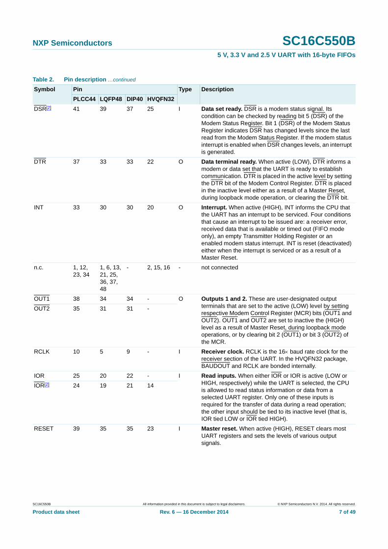
Table 2. Pin description
Symbol Pin Type Description
PLCC44 LQFP48 DIP40 HVQFN32
A0 31 28 28 19 I Register select. A2 to A0 are used during read and write operations to select the UART register to read from or write to. Refer to Table 3 for register addresses and refer to AS description.
A1 30 27 27 18
A2 29 26 26 17
AS 28 24 25 - I Address strobe. When AS is active (LOW), A0, A1, and A2 and CS0, CS1, and CS2 drive the internal select logic directly; when AS is HIGH, the register select and chip select signals are held at the logic levels they were in when the LOW-to-HIGH transition of AS occurred.
BAUDOUT 17 12 15 - O Baud out. BAUDOUT is a 16 clock signal for the transmitter section of the UART. The clock rate is established by the reference oscillator frequency divided by a divisor specified in the baud generator divisor latches. BAUDOUT may also be used for the receiver section by tying this output to RCLK. In HVQFN32 package BAUDOUT and RCLK are bonded internally.
CS0[2] 14 9 12 - I Chip select. When CS0 and CS1 are HIGH and CS2 is LOW, these three inputs select the UART. When any of these inputs are inactive, the UART remains inactive (refer to AS description).
CS1[2] 15 10 13 -
CS2[2] 16 11 14 -
CS[2] - - - 8
CTS[2] 40 38 36 24 I Clear to send. CTS is a modem status signal. Its condition can be checked by reading bit 4 (CTS) of the Modem Status Register. Bit 0 (CTS) of the Modem Status Register indicates that CTS has changed states since the last read from the Modem Status Register. If the modem status interrupt is enabled when CTS changes levels and the auto-CTS mode is not enabled, an interrupt is generated. This pin has no effect on the UART’s transmit or receive operation.
D7 to D0 9, 8, 7, 6, 5, 4, 3, 2
4, 3, 2, 47, 46, 45, 44, 43
8, 7, 6, 5, 4, 3, 2, 1
5, 4, 3, 1, 32, 31, 30, 29
I/O Data bus. Eight data lines with 3-state outputs provide a bidirectional path for data, control and status information between the UART and the CPU.
DCD[2] 42 40 38 26 I Data carrier detect. DCD is a modem status signal. Its condition can be checked by reading bit 7 (DCD) of the Modem Status Register. Bit 3 (DCD) of the Modem Status Register indicates that DCD has changed states since the last read from the Modem Status Register. If the modem status interrupt is enabled when DCD changes levels, an interrupt is generated.
DDIS 26 22 23 - O Driver disable. DDIS is active (LOW) when the CPU is reading data. When inactive (HIGH), DDIS can disable an external transceiver.
SC16C550B All information provided in this document is subject to legal disclaimers. © NXP Semiconductors N.V. 2014. All rights reserved.
Product data sheet Rev. 6 — 16 December 2014 6 of 49
NXP Semiconductors SC16C550B5 V, 3.3 V and 2.5 V UART with 16-byte FIFOs
DSR[2] 41 39 37 25 I Data set ready. DSR is a modem status signal. Its condition can be checked by reading bit 5 (DSR) of the Modem Status Register. Bit 1 (DSR) of the Modem Status Register indicates DSR has changed levels since the last read from the Modem Status Register. If the modem status interrupt is enabled when DSR changes levels, an interrupt is generated.
DTR 37 33 33 22 O Data terminal ready. When active (LOW), DTR informs a modem or data set that the UART is ready to establish communication. DTR is placed in the active level by setting the DTR bit of the Modem Control Register. DTR is placed in the inactive level either as a result of a Master Reset, during loopback mode operation, or clearing the DTR bit.
INT 33 30 30 20 O Interrupt. When active (HIGH), INT informs the CPU that the UART has an interrupt to be serviced. Four conditions that cause an interrupt to be issued are: a receiver error, received data that is available or timed out (FIFO mode only), an empty Transmitter Holding Register or an enabled modem status interrupt. INT is reset (deactivated) either when the interrupt is serviced or as a result of a Master Reset.
n.c. 1, 12, 23, 34
1, 6, 13, 21, 25, 36, 37, 48
- 2, 15, 16 - not connected
OUT1 38 34 34 - O Outputs 1 and 2. These are user-designated output terminals that are set to the active (LOW) level by setting respective Modem Control Register (MCR) bits (OUT1 and OUT2). OUT1 and OUT2 are set to inactive the (HIGH) level as a result of Master Reset, during loopback mode operations, or by clearing bit 2 (OUT1) or bit 3 (OUT2) of the MCR.
OUT2 35 31 31 -
RCLK 10 5 9 - I Receiver clock. RCLK is the 16 baud rate clock for the receiver section of the UART. In the HVQFN32 package, BAUDOUT and RCLK are bonded internally.
IOR 25 20 22 - I Read inputs. When either IOR or IOR is active (LOW or HIGH, respectively) while the UART is selected, the CPU is allowed to read status information or data from a selected UART register. Only one of these inputs is required for the transfer of data during a read operation; the other input should be tied to its inactive level (that is, IOR tied LOW or IOR tied HIGH).
IOR[2] 24 19 21 14
RESET 39 35 35 23 I Master reset. When active (HIGH), RESET clears most UART registers and sets the levels of various output signals.
Table 2. Pin description …continued
Symbol Pin Type Description
PLCC44 LQFP48 DIP40 HVQFN32
SC16C550B All information provided in this document is subject to legal disclaimers. © NXP Semiconductors N.V. 2014. All rights reserved.
Product data sheet Rev. 6 — 16 December 2014 7 of 49

NXP Semiconductors SC16C550B5 V, 3.3 V and 2.5 V UART with 16-byte FIFOs
RI[2] 43 41 39 27 I Ring indicator. RI is a modem status signal. Its condition can be checked by reading bit 6 (RI) of the Modem Status Register. Bit 2 (RI) of the Modem Status Register indicates that RI has changed from a LOW to a HIGH level since the last read from the Modem Status Register. If the modem status interrupt is enabled when this transition occurs, an interrupt is generated.
RTS 36 32 32 21 O Request to send. When active, RTS informs the modem or data set that the UART is ready to receive data. RTS is set to the active level by setting the RTS Modem Control Register bit and is set to the inactive (HIGH) level either as a result of a Master Reset or during loopback mode operations or by clearing bit 1 (RTS) of the MCR. This pin has no effect on the UART’s transmit or receive operation.
RXRDY 32 29 29 - O Receiver ready. Receiver Direct Memory Access (DMA) signaling is available with RXRDY. When operating in the FIFO mode, one of two types of DMA signaling can be selected using the FIFO Control Register bit 3 (FCR[3]). When operating in the 16C450 mode, only DMA mode 0 is allowed. Mode 0 supports single-transfer DMA in which a transfer is made between CPU bus cycles. Mode 1 supports multi-transfer DMA in which multiple transfers are made continuously until the receiver FIFO has been emptied. In DMA mode 0 (FCR[0] = 0 or FCR[0] = 1, FCR[3] = 0), when there is at least one character in the receiver FIFO or Receiver Holding Register, RXRDY is active (LOW). When RXRDY has been active but there are no characters in the FIFO or holding register, RXRDY goes inactive (HIGH). In DMA mode 1 (FCR[0] = 1, FCR[3] = 1), when the trigger level or the time-out has been reached, RXRDY goes active (LOW); when it has been active but there are no more characters in the FIFO or holding register, it goes inactive (HIGH). This function does not exist in the HVQFN32 package.
RX 11 7 10 6 I Serial data input. RX is serial data input from a connected communications device.
TX 13 8 11 7 O Serial data output. TX is composite serial data output to a connected communication device. TX is set to the marking (HIGH) level as a result of Master Reset.
TXRDY 27 23 24 - O Transmitter ready. Transmitter DMA signaling is available with TXRDY. When operating in the FIFO mode, one of two types of DMA signaling can be selected using FCR[3]. When operating in the 16C450 mode, only DMA mode 0 is allowed. Mode 0 supports single-transfer DMA in which a transfer is made between CPU bus cycles. Mode 1 supports multi-transfer DMA in which multiple transfers are made continuously until the transmit FIFO has been filled. This function does not exist in the HVQFN32 package.
VDD 44 42 40 28 power 2.5 V, 3.3 V or 5 V supply voltage.
VSS 22 18 20 9, 13[1] power Ground voltage.
Table 2. Pin description …continued
Symbol Pin Type Description
PLCC44 LQFP48 DIP40 HVQFN32
SC16C550B All information provided in this document is subject to legal disclaimers. © NXP Semiconductors N.V. 2014. All rights reserved.
Product data sheet Rev. 6 — 16 December 2014 8 of 49
NXP Semiconductors SC16C550B5 V, 3.3 V and 2.5 V UART with 16-byte FIFOs
[1] HVQFN32 package die supply ground is connected to both the VSS pin and the exposed center pad. The VSS pin must be connected to supply ground for proper device operation. For enhanced thermal, electrical, and board-level performance, the exposed pad needs to be soldered to the board using a corresponding thermal pad on the board, and for proper heat conduction through the board thermal vias need to be incorporated in the Printed-Circuit Board (PCB) in the thermal pad region.
[2] This pin has a pull-up resistor.
[3] In Sleep mode, XTAL2 is left floating.
6. Functional description
The SC16C550B provides serial asynchronous receive data synchronization, parallel-to-serial and serial-to-parallel data conversions for both the transmitter and receiver sections. These functions are necessary for converting the serial data stream into parallel data that is required with digital data systems. Synchronization for the serial data stream is accomplished by adding start and stop bits to the transmit data to form a data character (character orientated protocol). Data integrity is insured by attaching a parity bit to the data character. The parity bit is checked by the receiver for any transmission bit errors. The SC16C550B is fabricated with an advanced CMOS process to achieve low drain power and high speed requirements.
The SC16C550B is an upward solution that provides 16 bytes of transmit and receive FIFO memory, instead of none in the 16C450. The SC16C550B is designed to work with high speed modems and shared network environments that require fast data processing time. Increased performance is realized in the SC16C550B by the larger transmit and receive FIFOs. This allows the external processor to handle more networking tasks within a given time. In addition, the four selectable levels of FIFO trigger interrupt are provided for maximum data throughput performance, especially when operating in a multi-channel environment. The combination of the above greatly reduces the bandwidth requirement of the external controlling CPU, increases performance, and reduces power consumption.
The SC16C550B is capable of operation up to 3 Mbit/s with a 48 MHz external clock input (at 5 V).
IOW 21 17 19 - I Write inputs. When either IOW or IOW is active (LOW or HIGH, respectively) and while the UART is selected, the CPU is allowed to write control words or data into a selected UART register. Only one of these inputs is required to transfer data during a write operation; the other input should be tied to its inactive level (that is, IOW tied LOW or IOW tied HIGH).
IOW[2] 20 16 18 12
XTAL1 18 14 16 10 I Crystal connection or External clock input.
XTAL2[3] 19 15 17 11 O Crystal connection or the inversion of XTAL1 if XTAL1 is driven.
Table 2. Pin description …continued
Symbol Pin Type Description
PLCC44 LQFP48 DIP40 HVQFN32
SC16C550B All information provided in this document is subject to legal disclaimers. © NXP Semiconductors N.V. 2014. All rights reserved.
Product data sheet Rev. 6 — 16 December 2014 9 of 49

NXP Semiconductors SC16C550B5 V, 3.3 V and 2.5 V UART with 16-byte FIFOs
6.1 Internal registers
The SC16C550B provides 12 internal registers for monitoring and control. These registers are shown in Table 3. These registers function as data holding registers (THR/RHR), interrupt status and control registers (IER/ISR), a FIFO Control Register (FCR), line status and control registers (LCR/LSR), modem status and control registers (MCR/MSR), programmable data rate (clock) control registers (DLL/DLM), and a user accessible scratchpad register (SPR). Register functions are more fully described in the following paragraphs.
[1] These registers are accessible only when LCR[7] is a logic 0.
[2] These registers are accessible only when LCR[7] is a logic 1.
6.2 FIFO operation
The 16-byte transmit and receive data FIFOs are enabled by the FIFO Control Register bit 0 (FCR[0]). With 16C550 devices, the user can set the receive trigger level, but not the transmit trigger level. The receiver FIFO section includes a time-out function to ensure data is delivered to the external CPU. An interrupt is generated whenever the Receive Holding Register (RHR) has not been read following the loading of a character or the receive trigger level has not been reached.
Table 3. Internal registers decoding
A2 A1 A0 Read mode Write mode
General register set (THR/RHR, IER/ISR, MCR/MSR, FCR/LSR, SPR)[1]
0 0 0 Receive Holding Register Transmit Holding Register
0 0 1 Interrupt Enable Register Interrupt Enable Register
0 1 0 Interrupt Status Register FIFO Control Register
0 1 1 Line Control Register Line Control Register
1 0 0 Modem Control Register Modem Control Register
1 0 1 Line Status Register n/a
1 1 0 Modem Status Register n/a
1 1 1 Scratchpad Register Scratchpad Register
Baud rate register set (DLL/DLM)[2]
0 0 0 LSB of Divisor Latch LSB of Divisor Latch
0 0 1 MSB of Divisor Latch MSB of Divisor Latch
Table 4. Flow control mechanism
Selected trigger level (characters)
INT pin activation Negate RTS Assert RTS
1 1 1 0
4 4 4 0
8 8 8 0
14 14 14 0
SC16C550B All information provided in this document is subject to legal disclaimers. © NXP Semiconductors N.V. 2014. All rights reserved.
Product data sheet Rev. 6 — 16 December 2014 10 of 49

NXP Semiconductors SC16C550B5 V, 3.3 V and 2.5 V UART with 16-byte FIFOs
6.3 Autoflow control
Autoflow control is comprised of auto-CTS and auto-RTS (see Figure 6). With auto-CTS, the CTS input must be active before the transmitter FIFO can emit data. With auto-RTS, RTS becomes active when the receiver needs more data and notifies the sending serial device. When RTS is connected to CTS, data transmission does not occur unless the receiver FIFO has space for the data; thus, overrun errors are eliminated using UART 1 and UART 2 from a SC16C550B with the autoflow control enabled. If not, overrun errors occur when the transmit data rate exceeds the receiver FIFO read latency.
6.3.1 Auto-RTS
Auto-RTS data flow control originates in the receiver timing and control block (refer to Figure 1 “Block diagram of SC16C550B”) and is linked to the programmed receiver FIFO trigger level (see Figure 6). When the receiver FIFO level reaches a trigger level of 1, 4, or 8 (see Figure 8), RTS is de-asserted. With trigger levels of 1, 4, and 8, the sending UART may send an additional byte after the trigger level is reached (assuming the sending UART has another byte to send) because it may not recognize the de-assertion of RTS until after it has begun sending the additional byte. RTS is automatically reasserted once the RX FIFO is emptied by reading the receiver buffer register. When the trigger level is 14 (see Figure 9), RTS is de-asserted after the first data bit of the 16th character is present on the RX line. RTS is reasserted when the RX FIFO has at least one available byte space.
6.3.2 Auto-CTS
The transmitter circuitry checks CTS before sending the next data byte (see Figure 6). When CTS is active, it sends the next byte. To stop the transmitter from sending the following byte, CTS must be released before the middle of the last stop bit that is currently being sent (see Figure 7). The auto-CTS function reduces interrupts to the host system. When flow control is enabled, CTS level changes do not trigger host interrupts because the device automatically controls its own transmitter. Without auto-CTS, the transmitter sends any data present in the transmit FIFO and a receiver overrun error may result.
Fig 6. Autoflow control (auto-RTS and auto-CTS) example
RXFIFO
FLOWCONTROL
TXFIFO
PARALLELTO SERIAL
TXFIFO
RXFIFO
UART 1 UART 2
D7 to D0
RX TX
RTS CTS
TX RX
CTS RTS
D7 to D0
002aaa228
SERIAL TO PARALLEL
SERIAL TO PARALLEL
FLOWCONTROL
FLOWCONTROL
FLOWCONTROL
PARALLELTO SERIAL
SC16C550B All information provided in this document is subject to legal disclaimers. © NXP Semiconductors N.V. 2014. All rights reserved.
Product data sheet Rev. 6 — 16 December 2014 11 of 49

NXP Semiconductors SC16C550B5 V, 3.3 V and 2.5 V UART with 16-byte FIFOs
6.3.3 Enabling autoflow control and auto-CTS
Autoflow control is enabled by setting MCR[5] and MCR[1].
6.3.4 Auto-CTS and auto-RTS functional timing
The receiver FIFO trigger level can be set to 1, 4, 8, or 14 bytes. These are described in Figure 8 and Figure 9.
Table 5. Enabling autoflow control and auto-CTS
MCR[5] MCR[1] Selection
1 1 auto RTS and CTS
1 0 auto CTS
0 X disable
(1) When CTS is LOW, the transmitter keeps sending serial data out.
(2) If CTS goes HIGH before the middle of the last stop bit of the current byte, the transmitter finishes sending the current byte, but it does not send the next byte.
(3) When CTS goes from HIGH to LOW, the transmitter begins sending data again.
Fig 7. CTS functional timing waveforms
Start bits 0 to 7 StopTX
CTS
002aaa049
Start bits 0 to 7 Stop Start bits 0 to 7 Stop
(1) N = RX FIFO trigger level (1, 4, or 8 bytes).
(2) The two blocks in dashed lines cover the case where an additional byte is sent as described in Section 6.3.1.
Fig 8. RTS functional timing waveforms, RX FIFO trigger level = 1, 4, or 8 bytes
Start byte N Start byte N + 1 Start byteStop Stop StopRX
RTS
IOR N N + 11 2
002aaa050
SC16C550B All information provided in this document is subject to legal disclaimers. © NXP Semiconductors N.V. 2014. All rights reserved.
Product data sheet Rev. 6 — 16 December 2014 12 of 49

NXP Semiconductors SC16C550B5 V, 3.3 V and 2.5 V UART with 16-byte FIFOs
6.4 Hardware/software and time-out interrupts
Following a reset, the transmitter interrupt is enabled, the SC16C550B will issue an interrupt to indicate that the Transmit Holding Register is empty. This interrupt must be serviced prior to continuing operations. The ISR register provides the current singular highest priority interrupt only. Only after servicing the higher pending interrupt will the lower priority be reflected in the status register. Servicing the interrupt without investigating further interrupt conditions can result in data errors.
When two interrupt conditions have the same priority, it is important to service these interrupts correctly. Receive Data Ready and Receive Time-Out have the same interrupt priority (when enabled by IER[0]). The receiver issues an interrupt after the number of characters have reached the programmed trigger level. In this case, the SC16C550B FIFO may hold more characters than the programmed trigger level. Following the removal of a data byte, the user should re-check LSR[0] for additional characters. A Receive Time-Out will not occur if the receive FIFO is empty. The time-out counter is reset at the center of each stop bit received or each time the Receive Holding Register (RHR) is read. The actual time-out value is 4 character time, including data information length, start bit, parity bit, and the size of stop bit, that is, 1, 1.5, or 2 bit times.
(1) RTS is de-asserted when the receiver receives the first data bit of the sixteenth byte. The receive FIFO is full after finishing the sixteenth byte.
(2) RTS is asserted again when there is at least one byte of space available and no incoming byte is in processing, or there is more than one byte of space available.
(3) When the receive FIFO is full, the first receive buffer register read re-asserts RTS.
Fig 9. RTS functional timing waveforms, RX FIFO trigger level = 14 bytes
byte 14 byte 15RX
RTS
IOR
Start byte 18 StopStart byte 16 Stop
002aaa051
RTS released after the first data bit of byte 16
SC16C550B All information provided in this document is subject to legal disclaimers. © NXP Semiconductors N.V. 2014. All rights reserved.
Product data sheet Rev. 6 — 16 December 2014 13 of 49
NXP Semiconductors SC16C550B5 V, 3.3 V and 2.5 V UART with 16-byte FIFOs
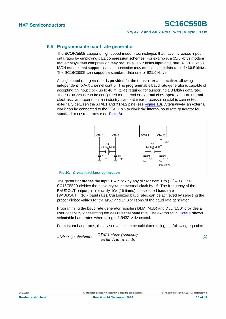
6.5 Programmable baud rate generator
The SC16C550B supports high speed modem technologies that have increased input data rates by employing data compression schemes. For example, a 33.6 kbit/s modem that employs data compression may require a 115.2 kbit/s input data rate. A 128.0 kbit/s ISDN modem that supports data compression may need an input data rate of 460.8 kbit/s. The SC16C550B can support a standard data rate of 921.6 kbit/s.
A single baud rate generator is provided for the transmitter and receiver, allowing independent TX/RX channel control. The programmable baud rate generator is capable of accepting an input clock up to 48 MHz, as required for supporting a 3 Mbit/s data rate. The SC16C550B can be configured for internal or external clock operation. For internal clock oscillator operation, an industry standard microprocessor crystal is connected externally between the XTAL1 and XTAL2 pins (see Figure 10). Alternatively, an external clock can be connected to the XTAL1 pin to clock the internal baud rate generator for standard or custom rates (see Table 6).
The generator divides the input 16 clock by any divisor from 1 to (216 1). The SC16C550B divides the basic crystal or external clock by 16. The frequency of the BAUDOUT output pin is exactly 16 (16 times) the selected baud rate (BAUDOUT = 16 baud rate). Customized baud rates can be achieved by selecting the proper divisor values for the MSB and LSB sections of the baud rate generator.
Programming the baud rate generator registers DLM (MSB) and DLL (LSB) provides a user capability for selecting the desired final baud rate. The examples in Table 6 shows selectable baud rates when using a 1.8432 MHz crystal.
For custom baud rates, the divisor value can be calculated using the following equation:
(1)
Fig 10. Crystal oscillator connection
002aaa870
C247 pF
XTAL1 XTAL2
X11.8432 MHz
C122 pF
C233 pF
XTAL1 XTAL2
1.5 kΩX1
1.8432 MHz
C122 pF
divisor in decimal XTAL1 clock frequencyserial data rate 16
---------------------------------------------------------------=
SC16C550B All information provided in this document is subject to legal disclaimers. © NXP Semiconductors N.V. 2014. All rights reserved.
Product data sheet Rev. 6 — 16 December 2014 14 of 49

NXP Semiconductors SC16C550B5 V, 3.3 V and 2.5 V UART with 16-byte FIFOs
6.6 DMA operation
The SC16C550B FIFO trigger level provides additional flexibility to the user for block mode operation. The user can optionally operate the transmit and receive FIFOs in the DMA mode (FCR[3]). The DMA mode affects the state of the RXRDY and TXRDY output pins. Table 7 and Table 8 show this.
Remark: DMA operation is not supported in the HVQFN32 package.
Table 6. Baud rates using 1.8432 MHz or 3.072 MHz crystal
Using 1.8432 MHz crystal Using 3.072 MHz crystal
Desired baud rate
Divisor for 16 clock
Baud rate error
Desired baud rate
Divisor for 16 clock
Baud rate error
50 2304 50 3840
75 1536 75 2560
110 1047 0.026 110 1745 0.026
134.5 857 0.058 134.5 1428 0.034
150 768 150 1280
300 384 300 640
600 192 600 320
1200 96 1200 160
1800 64 1800 107 0.312
2000 58 0.69 2000 96
2400 48 2400 80
3600 32 3600 53 0.628
4800 24 4800 40
7200 16 7200 27 1.23
9600 12 9600 20
19200 6 19200 10
38400 3 38400 5
56000 2 2.86
Table 7. Effect of DMA mode on state of RXRDY pin
Non-DMA mode DMA mode
1 = FIFO empty 0-to-1 transition when FIFO empties
0 = at least 1 byte in FIFO 1-to-0 transition when FIFO reaches trigger level, or time-out occurs
Table 8. Effect of DMA mode on state of TXRDY pin
Non-DMA mode DMA mode
1 = at least 1 byte in FIFO 1 = FIFO is full
0 = FIFO empty 0 = FIFO is empty
SC16C550B All information provided in this document is subject to legal disclaimers. © NXP Semiconductors N.V. 2014. All rights reserved.
Product data sheet Rev. 6 — 16 December 2014 15 of 49

NXP Semiconductors SC16C550B5 V, 3.3 V and 2.5 V UART with 16-byte FIFOs
6.7 Loopback mode
The internal loopback capability allows on-board diagnostics. In the loopback mode, the normal modem interface pins are disconnected and reconfigured for loopback internally. MCR[3:0] register bits are used for controlling loopback diagnostic testing. In the loopback mode, OUT1 (bit 2) and OUT2 (bit 3) in the MCR register control the modem RI and DCD inputs, respectively. MCR signals DTR and RTS (bits 0:1) are used to control the modem CTS and DSR inputs, respectively. The transmitter output (TX) and the receiver input (RX) are disconnected from their associated interface pins, and instead are connected together internally (see Figure 11). The inputs CTS, DSR, DCD, and RI are disconnected from their normal modem control input pins, and instead are connected internally to DTR, RTS, OUT1 and OUT2. Loopback test data is entered into the transmit holding register via the user data bus interface, D0 to D7. The transmit UART serializes the data and passes the serial data to the receive UART via the internal loopback connection. The receive UART converts the serial data back into parallel data that is then made available at the user data interface D0 to D7. The user optionally compares the received data to the initial transmitted data for verifying error-free operation of the UART TX/RX circuits.
In this mode, the receiver and transmitter interrupts are fully operational. The Modem Control Interrupts are also operational. However, the interrupts can only be read using the lower four bits of the Modem Status Register (MSR[3:0]) instead of the four Modem Status Register bits 7:4. The interrupts are still controlled by the IER.
SC16C550B All information provided in this document is subject to legal disclaimers. © NXP Semiconductors N.V. 2014. All rights reserved.
Product data sheet Rev. 6 — 16 December 2014 16 of 49

NXP Semiconductors SC16C550B5 V, 3.3 V and 2.5 V UART with 16-byte FIFOs
Fig 11. Internal loopback mode diagram
CTS
TRANSMITFIFO
REGISTERS
TX
RECEIVESHIFT
REGISTER
RECEIVEFIFO
REGISTERSRX
INT
ER
CO
NN
EC
T B
US
LIN
ES
AN
DC
ON
TR
OL
SIG
NA
LS
SC16C550B
TRANSMITSHIFT
REGISTER
002aaa587
DATA BUSAND
CONTROLLOGIC
REGISTERSELECTLOGIC
INTERRUPTCONTROL
LOGIC
D0 to D7IOR, IOR
IOW, IOWRESET
INTTXRDYRXRDY
CLOCK ANDBAUD RATE
GENERATOR
MODEMCONTROL
LOGIC
RTS
DSR
DTR
RI
OUT1
DCD
OUT2
MCR[4] = 1
XTAL2BAUDOUT
XTAL1RCLK
DDIS
A0 to A2CS0, CS1, CS2
AS
SC16C550B All information provided in this document is subject to legal disclaimers. © NXP Semiconductors N.V. 2014. All rights reserved.
Product data sheet Rev. 6 — 16 December 2014 17 of 49

NXP Semiconductors SC16C550B5 V, 3.3 V and 2.5 V UART with 16-byte FIFOs
7. Register descriptions
Table 9 details the assigned bit functions for the twelve SC16C550B internal registers. The assigned bit functions are more fully defined in Section 7.1 through Section 7.10.
[1] The value shown represents the register’s initialized hexadecimal value; X = not applicable.
[2] These registers are accessible only when LCR[7] is set to a logic 0.
[3] These functions are not supported in the HVQFN32 package, and should not be written.
[4] OUT2 pin is not supported in the HVQFN32 package. MCR3 is INT enabled in the HVQFN32 package. INT is always enabled in DIP40, PLCC44 and LQFP48 packages.
[5] The Special Register set is accessible only when LCR[7] is set to a logic 1.
Table 9. SC16C550B internal registers
A2 A1 A0 Register Default [1]
Bit 7 Bit 6 Bit 5 Bit 4 Bit 3 Bit 2 Bit 1 Bit 0
General Register Set[2]
0 0 0 RHR XX bit 7 bit 6 bit 5 bit 4 bit 3 bit 2 bit 1 bit 0
0 0 0 THR XX bit 7 bit 6 bit 5 bit 4 bit 3 bit 2 bit 1 bit 0
0 0 1 IER 00 modem status interrupt
receive line status interrupt
transmit holding register
receive holding register
0 1 0 FCR 00 RX trigger (MSB)
RX trigger (LSB)
reserved reserved DMA mode select[3]
TX FIFO reset
RX FIFO reset
FIFO enable
0 1 0 ISR 01 FIFOs enabled
FIFOs enabled
0 0 INT priority bit 2
INT priority bit 1
INT priority bit 0
INT status
0 1 1 LCR 00 divisor latch enable
set break set parity even parity
parity enable
stop bits word length bit 1
word length bit 0
1 0 0 MCR 00 reserved auto flow control enable
loopback OUT2, INT enable[4]
OUT1[3] RTS DTR
1 0 1 LSR 60 FIFO data error
transmit empty
transmit holding empty
break interrupt
framing error
parity error
overrun error
receive data ready
1 1 0 MSR X0 DCD RI DSR CTS DCD RI DSR CTS
1 1 1 SPR FF bit 7 bit 6 bit 5 bit 4 bit 3 bit 2 bit 1 bit 0
Special Register Set[5]
0 0 0 DLL XX bit 7 bit 6 bit 5 bit 4 bit 3 bit 2 bit 1 bit 0
0 0 1 DLM XX bit 15 bit 14 bit 13 bit 12 bit 11 bit 10 bit 9 bit 8
SC16C550B All information provided in this document is subject to legal disclaimers. © NXP Semiconductors N.V. 2014. All rights reserved.
Product data sheet Rev. 6 — 16 December 2014 18 of 49
NXP Semiconductors SC16C550B5 V, 3.3 V and 2.5 V UART with 16-byte FIFOs
7.1 Transmit Holding Register (THR) and Receive Holding Register (RHR)
The serial transmitter section consists of an 8-bit Transmit Holding Register (THR) and Transmit Shift Register (TSR). The status of the THR is provided in the Line Status Register (LSR). Writing to the THR transfers the contents of the data bus (D[7:0]) to the THR, providing that the THR or TSR is empty. The THR empty flag in the LSR register will be set to a logic 1 when the transmitter is empty or when data is transferred to the TSR. Note that a write operation can be performed when the THR empty flag is set (logic 0 = FIFO full; logic 1 = at least one FIFO location available).
The serial receive section also contains an 8-bit Receive Holding Register (RHR). Receive data is removed from the SC16C550B and receive FIFO by reading the RHR register. The receive section provides a mechanism to prevent false starts. On the falling edge of a start or false start bit, an internal receiver counter starts counting clocks at the 16 clock rate. After 71⁄2 clocks, the start bit time should be shifted to the center of the start bit. At this time the start bit is sampled, and if it is still a logic 0 it is validated. Evaluating the start bit in this manner prevents the receiver from assembling a false character. Receiver status codes will be posted in the LSR.
7.2 Interrupt Enable Register (IER)
The Interrupt Enable Register (IER) masks the interrupts from receiver ready, transmitter empty, line status and modem status registers. These interrupts would normally be seen on the INT output pin.
Table 10. Interrupt Enable Register bits description
Bit Symbol Description
7:4 IER[7:4] not used
3 IER[3] Modem Status Interrupt.
logic 0 = disable the modem status register interrupt (normal default condition)
logic 1 = enable the modem status register interrupt
2 IER[2] Receive Line Status interrupt. This interrupt will be issued whenever a fully assembled receive character is transferred from RSR to the RHR/FIFO, that is, data ready, LSR[0].
logic 0 = disable the receiver line status interrupt (normal default condition)
logic 1 = enable the receiver line status interrupt
1 IER[1] Transmit Holding Register interrupt. This interrupt will be issued whenever the THR is empty, and is associated with LSR[1].
logic 0 = disable the transmitter empty interrupt (normal default condition)
logic 1 = enable the transmitter empty interrupt
0 IER[0] Receive Holding Register interrupt. This interrupt will be issued when the FIFO has reached the programmed trigger level, or is cleared when the FIFO drops below the trigger level in the FIFO mode of operation.
logic 0 = disable the receiver ready interrupt (normal default condition)
logic 1 = enable the receiver ready interrupt
SC16C550B All information provided in this document is subject to legal disclaimers. © NXP Semiconductors N.V. 2014. All rights reserved.
Product data sheet Rev. 6 — 16 December 2014 19 of 49

NXP Semiconductors SC16C550B5 V, 3.3 V and 2.5 V UART with 16-byte FIFOs
7.2.1 IER versus Receive FIFO interrupt mode operation
When the receive FIFO (FCR[0] = logic 1), and receive interrupts (IER[0] = logic 1) are enabled, the receive interrupts and register status will reflect the following:
• The receive data available interrupts are issued to the external CPU when the FIFO has reached the programmed trigger level. It will be cleared when the FIFO drops below the programmed trigger level.
• FIFO status will also be reflected in the user accessible ISR register when the FIFO trigger level is reached. Both the ISR register status bit and the interrupt will be cleared when the FIFO drops below the trigger level.
• The data ready bit (LSR[0]) is set as soon as a character is transferred from the shift register to the receive FIFO. It is reset when the FIFO is empty.
7.2.2 IER versus Receive/Transmit FIFO polled mode operation
When FCR[0] = logic 1, resetting IER[0:3] enables the SC16C550B in the FIFO polled mode of operation. Since the receiver and transmitter have separate bits in the LSR, either or both can be used in the polled mode by selecting respective transmit or receive control bit(s).
• LSR[0] will be a logic 1 as long as there is one byte in the receive FIFO.
• LSR[1:4] will provide the type of errors encountered, if any.
• LSR[5] will indicate when the transmit FIFO is empty.
• LSR[6] will indicate when both the transmit FIFO and transmit shift register are empty.
• LSR[7] will indicate any FIFO data errors.
7.3 FIFO Control Register (FCR)
This register is used to enable the FIFOs, clear the FIFOs, set the receive FIFO trigger levels, and select the DMA mode.
7.3.1 DMA mode
(DMA mode does not exist in the HVQFN32 package; see Table 9.)
7.3.1.1 Mode 0 (FCR bit 3 = 0)
Set and enable the interrupt for each single transmit or receive operation, and is similar to the 16C450 mode. Transmit Ready (TXRDY) will go to a logic 0 whenever an empty transmit space is available in the Transmit Holding Register (THR). Receive Ready (RXRDY) will go to a logic 0 whenever the Receive Holding Register (RHR) is loaded with a character.
7.3.1.2 Mode 1 (FCR bit 3 = 1)
Set and enable the interrupt in a block mode operation. The transmit interrupt is set when the transmit FIFO is empty. The receive interrupt is set when the receive FIFO fills to the programmed trigger level. However, the FIFO continues to fill regardless of the programmed level until the FIFO is full. RXRDY remains a logic 0 as long as the FIFO fill level is above the programmed trigger level.
SC16C550B All information provided in this document is subject to legal disclaimers. © NXP Semiconductors N.V. 2014. All rights reserved.
Product data sheet Rev. 6 — 16 December 2014 20 of 49

NXP Semiconductors SC16C550B5 V, 3.3 V and 2.5 V UART with 16-byte FIFOs
7.3.2 FIFO mode
Table 11. FIFO Control Register bits description
Bit Symbol Description
7:6 FCR[7] (MSB), FCR[6] (LSB)
RX trigger. These bits are used to set the trigger level for the receive FIFO interrupt.
An interrupt is generated when the number of characters in the FIFO equals the programmed trigger level. However, the FIFO will continue to be loaded until it is full. Refer to Table 12.
5:4 FCR[5] (MSB), FCR[4] (LSB)
not used; set to 00
3 FCR[3] DMA mode select.
logic 0 = set DMA mode ‘0’ (normal default condition)
logic 1 = set DMA mode ‘1’
Transmit operation in mode ‘0’: When the SC16C550B is in the 16C450 mode (FIFOs disabled; FCR[0] = logic 0) or in the FIFO mode (FIFOs enabled; FCR[0] = logic 1; FCR[3] = logic 0), and when there are no characters in the transmit FIFO or transmit holding register, the TXRDY pin will be a logic 0. Once active, the TXRDY pin will go to a logic 1 after the first character is loaded into the transmit holding register.
Receive operation in mode ‘0’: When the SC16C550B is in 16C450 mode, or in the FIFO mode (FCR[0] = logic 1; FCR[3] = logic 0) and there is at least one character in the receive FIFO, the RXRDY pin will be a logic 0. Once active, the RXRDY pin will go to a logic 1 when there are no more characters in the receiver.
Transmit operation in mode ‘1’: When the SC16C550B is in FIFO mode (FCR[0] = logic 1; FCR[3] = logic 1), the TXRDY pin will be a logic 1 when the transmit FIFO is completely full. It will be a logic 0 if the transmit FIFO is completely empty.
Receive operation in mode ‘1’: When the SC16C550B is in FIFO mode (FCR[0] = logic 1; FCR[3] = logic 1) and the trigger level has been reached, or a Receive Time-Out has occurred, the RXRDY pin will go to a logic 0. Once activated, it will go to a logic 1 after there are no more characters in the FIFO.
2 FCR[2] TX FIFO reset.
logic 0 = no FIFO transmit reset (normal default condition)
logic 1 = clears the contents of the transmit FIFO and resets the FIFO counter logic (the transmit shift register is not cleared or altered). This bit will return to a logic 0 after clearing the FIFO.
1 FCR[1] RX FIFO reset.
logic 0 = no FIFO receive reset (normal default condition)
logic 1 = clears the contents of the receive FIFO and resets the FIFO counter logic (the receive shift register is not cleared or altered). This bit will return to a logic 0 after clearing the FIFO.
0 FCR[0] FIFO enable.
logic 0 = disable the transmit and receive FIFO (normal default condition)
logic 1 = enable the transmit and receive FIFO. This bit must be a ‘1’ when other FCR bits are written to, or they will not be programmed.
SC16C550B All information provided in this document is subject to legal disclaimers. © NXP Semiconductors N.V. 2014. All rights reserved.
Product data sheet Rev. 6 — 16 December 2014 21 of 49

NXP Semiconductors SC16C550B5 V, 3.3 V and 2.5 V UART with 16-byte FIFOs
7.4 Interrupt Status Register (ISR)
The SC16C550B provides four levels of prioritized interrupts to minimize external software interaction. The Interrupt Status Register (ISR) provides the user with four interrupt status bits. Performing a read cycle on the ISR will provide the user with the highest pending interrupt level to be serviced. No other interrupts are acknowledged until the pending interrupt is serviced. Whenever the interrupt status register is read, the interrupt status is cleared. However, it should be noted that only the current pending interrupt is cleared by the read. A lower level interrupt may be seen after re-reading the interrupt status bits. Table 13 “Interrupt source” shows the data values (bits 3:0) for the four prioritized interrupt levels and the interrupt sources associated with each of these interrupt levels.
Table 12. RX trigger levels
FCR[7] FCR[6] RX FIFO trigger level (bytes)
0 0 1
0 1 4
1 0 8
1 1 14
Table 13. Interrupt source
Priority level
ISR[3] ISR[2] ISR[1] ISR[0] Source of the interrupt
1 0 1 1 0 LSR (Receiver Line Status Register)
2 0 1 0 0 RXRDY (Received Data Ready)
2 1 1 0 0 RXRDY (Receive Data time-out)
3 0 0 1 0 TXRDY (Transmitter Holding Register Empty)
4 0 0 0 0 MSR (Modem Status Register)
Table 14. Interrupt Status Register bits description
Bit Symbol Description
7:6 ISR[7:6] FIFOs enabled. These bits are set to a logic 0 when the FIFO is not being used. They are set to a logic 1 when the FIFOs are enabled.
logic 0 or cleared = default condition
5:4 ISR[5:4] not used
3:1 ISR[3:1] INT priority bits 2:0. These bits indicate the source for a pending interrupt at interrupt priority levels 1, 2, and 3 (see Table 13).
logic 0 or cleared = default condition
0 ISR[0] INT status.
logic 0 = an interrupt is pending and the ISR contents may be used as a pointer to the appropriate interrupt service routine
logic 1 = no interrupt pending (normal default condition)
SC16C550B All information provided in this document is subject to legal disclaimers. © NXP Semiconductors N.V. 2014. All rights reserved.
Product data sheet Rev. 6 — 16 December 2014 22 of 49

NXP Semiconductors SC16C550B5 V, 3.3 V and 2.5 V UART with 16-byte FIFOs
7.5 Line Control Register (LCR)
The Line Control Register is used to specify the asynchronous data communication format. The word length, the number of stop bits, and the parity are selected by writing the appropriate bits in this register.
Table 15. Line Control Register bits description
Bit Symbol Description
7 LCR[7] Divisor latch enable. The internal baud rate counter latch and Enhance Feature mode enable.
logic 0 = divisor latch disabled (normal default condition)
logic 1 = divisor latch and enhanced feature register enabled
6 LCR[6] Set break. When enabled, the Break control bit causes a break condition to be transmitted (the TX output is forced to a logic 0 state). This condition exists until disabled by setting LCR[6] to a logic 0.
logic 0 = no TX break condition (normal default condition)
logic 1 = forces the transmitter output (TX) to a logic 0 for alerting the remote receiver to a line break condition
5 LCR[5] Set parity. If the parity bit is enabled, LCR[5] selects the forced parity format. Programs the parity conditions (see Table 16).
logic 0 = parity is not forced (normal default condition)
LCR[5] = logic 1 and LCR[4] = logic 0: parity bit is forced to a logical 1 for the transmit and receive data
LCR[5] = logic 1 and LCR[4] = logic 1: parity bit is forced to a logical 0 for the transmit and receive data
4 LCR[4] Even parity. If the parity bit is enabled with LCR[3] set to a logic 1, LCR[4] selects the even or odd parity format.
logic 0 = odd parity is generated by forcing an odd number of logic 1s in the transmitted data. The receiver must be programmed to check the same format (normal default condition).
logic 1 = even parity is generated by forcing an even number of logic 1s in the transmitted data. The receiver must be programmed to check the same format.
3 LCR[3] Parity enable. Parity or no parity can be selected via this bit.
logic 0 = no parity (normal default condition)
logic 1 = a parity bit is generated during the transmission, receiver checks the data and parity for transmission errors
2 LCR[2] Stop bits. The length of stop bit is specified by this bit in conjunction with the programmed word length (see Table 17).
logic 0 or cleared = default condition
1:0 LCR[1:0] Word length bits [1:0]. These two bits specify the word length to be transmitted or received (see Table 18).
logic 0 or cleared = default condition
SC16C550B All information provided in this document is subject to legal disclaimers. © NXP Semiconductors N.V. 2014. All rights reserved.
Product data sheet Rev. 6 — 16 December 2014 23 of 49

NXP Semiconductors SC16C550B5 V, 3.3 V and 2.5 V UART with 16-byte FIFOs
Table 16. LCR[5] parity selection
LCR[5] LCR[4] LCR[3] Parity selection
X X 0 no parity
0 0 1 odd parity
0 1 1 even parity
1 0 1 forced parity ‘1’
1 1 1 forced parity ‘0’
Table 17. LCR[2] stop bit length
LCR[2] Word length Stop bit length (bit times)
0 5, 6, 7, 8 1
1 5 11⁄2
1 6, 7, 8 2
Table 18. LCR[1:0] word length
LCR[1] LCR[0] Word length
0 0 5
0 1 6
1 0 7
1 1 8
SC16C550B All information provided in this document is subject to legal disclaimers. © NXP Semiconductors N.V. 2014. All rights reserved.
Product data sheet Rev. 6 — 16 December 2014 24 of 49
NXP Semiconductors SC16C550B5 V, 3.3 V and 2.5 V UART with 16-byte FIFOs
7.6 Modem Control Register (MCR)
This register controls the interface with the modem or a peripheral device.
Table 19. Modem Control Register bits description
Bit Symbol Description
7 MCR[7] reserved; set to ‘0’
6 MCR[6] reserved; set to ‘0’
5 MCR[5] Auto flow control enable.
4 MCR[4] Loopback. Enable the local loopback mode (diagnostics). In this mode the transmitter output (TX) and the receiver input (RX), CTS, DSR, DCD, and RI are disconnected from the SC16C550B I/O pins. Internally the modem data and control pins are connected into a loopback data configuration (see Figure 11). In this mode, the receiver and transmitter interrupts remain fully operational. The Modem Control Interrupts are also operational, but the interrupts’ sources are switched to the lower four bits of the Modem Control. Interrupts continue to be controlled by the IER register.
logic 0 = disable loopback mode (normal default condition)
logic 1 = enable local loopback mode (diagnostics)
3 MCR[3] OUT2. Used to control the modem DCD signal in the loopback mode.
logic 0 = OUT2 is at logic 1. In the loopback mode, sets OUT2 (DCD) internally to a logic 1.
logic 1 = OUT2 is at logic 0. In the loopback mode, sets OUT2 (DCD) internally to a logic 0.
2 MCR[2] OUT1. This bit is used in the Loopback mode only. In the loopback mode, this bit is used to write the state of the modem RI interface signal via OUT1.
1 MCR[1] RTS
logic 0 = force RTS output to a logic 1 (normal default condition)
logic 1 = force RTS output to a logic 0
0 MCR[0] DTR
logic 0 = force DTR output to a logic 1 (normal default condition)
logic 1 = force DTR output to a logic 0
SC16C550B All information provided in this document is subject to legal disclaimers. © NXP Semiconductors N.V. 2014. All rights reserved.
Product data sheet Rev. 6 — 16 December 2014 25 of 49

NXP Semiconductors SC16C550B5 V, 3.3 V and 2.5 V UART with 16-byte FIFOs
7.7 Line Status Register (LSR)
This register provides the status of data transfers between the SC16C550B and the CPU.
Table 20. Line Status Register bits description
Bit Symbol Description
7 LSR[7] FIFO data error.
logic 0 = no error (normal default condition)
logic 1 = at least one parity error, framing error or break indication is in the current FIFO data. This bit is cleared when LSR register is read.
6 LSR[6] THR and TSR empty. This bit is the Transmit Empty indicator. This bit is set to a logic 1 whenever the transmit holding register and the transmit shift register are both empty. It is reset to logic 0 whenever either the THR or TSR contains a data character. In the FIFO mode, this bit is set to ‘1’ whenever the transmit FIFO and transmit shift register are both empty.
5 LSR[5] THR empty. This bit is the Transmit Holding Register Empty indicator. This bit indicates that the UART is ready to accept a new character for transmission. In addition, this bit causes the UART to issue an interrupt to CPU when the THR interrupt enable is set. The THR bit is set to a logic 1 when a character is transferred from the transmit holding register into the transmitter shift register. The bit is reset to a logic 0 concurrently with the loading of the transmitter holding register by the CPU. In the FIFO mode, this bit is set when the transmit FIFO is empty; it is cleared when at least 1 byte is written to the transmit FIFO.
4 LSR[4] Break interrupt.
logic 0 = no break condition (normal default condition)
logic 1 = the receiver received a break signal (RX was a logic 0 for one character frame time). In the FIFO mode, only one break character is loaded into the FIFO.
3 LSR[3] Framing error.
logic 0 = no framing error (normal default condition)
logic 1 = framing error. The receive character did not have a valid stop bit(s). In the FIFO mode, this error is associated with the character at the top of the FIFO.
2 LSR[2] Parity error.
logic 0 = no parity error (normal default condition)
logic 1 = parity error. The receive character does not have correct parity information and is suspect. In the FIFO mode, this error is associated with the character at the top of the FIFO.
1 LSR[1] Overrun error.
logic 0 = no overrun error (normal default condition)
logic 1 = overrun error. A data overrun error occurred in the receive shift register. This happens when additional data arrives while the FIFO is full. In this case, the previous data in the shift register is overwritten. Note that under this condition, the data byte in the receive shift register is not transferred into the FIFO, therefore the data in the FIFO is not corrupted by the error.
0 LSR[0] Receive data ready.
logic 0 = no data in receive holding register or FIFO (normal default condition)
logic 1 = data has been received and is saved in the receive holding register or FIFO
SC16C550B All information provided in this document is subject to legal disclaimers. © NXP Semiconductors N.V. 2014. All rights reserved.
Product data sheet Rev. 6 — 16 December 2014 26 of 49

NXP Semiconductors SC16C550B5 V, 3.3 V and 2.5 V UART with 16-byte FIFOs
7.8 Modem Status Register (MSR)
This register provides the current state of the control interface signals from the modem, or other peripheral device to which the SC16C550B is connected. Four bits of this register are used to indicate the changed information. These bits are set to a logic 1 whenever a control input from the modem changes state. These bits are set to a logic 0 whenever the CPU reads this register.
[1] Whenever any MSR bit 0:3 is set to logic 1, a Modem Status Interrupt will be generated.
Table 21. Modem Status Register bits description
Bit Symbol Description
7 MSR[7] Data Carrier Detect. DCD (active HIGH, logical 1). Normally this bit is the complement of the DCD input. In the loopback mode this bit is equivalent to the OUT2 bit in the MCR register.
6 MSR[6] Ring Indicator. RI (active HIGH, logical 1). Normally this bit is the complement of the RI input. In the loopback mode this bit is equivalent to the OUT1 bit in the MCR register.
5 MSR[5] Data Set Ready. DSR (active HIGH, logical 1). Normally this bit is the complement of the DSR input. In loopback mode this bit is equivalent to the DTR bit in the MCR register.
4 MSR[4] Clear To Send. CTS. CTS functions as hardware flow control signal input if it is enabled via MCR[5]. The transmit holding register flow control is enabled/disabled by MSR[4]. Flow control (when enabled) allows starting and stopping the transmissions based on the external modem CTS signal. A logic 1 at the CTS pin will stop SC16C550B transmissions as soon as current character has finished transmission. Normally MSR[4] is the complement of the CTS input. However, in the loopback mode, this bit is equivalent to the RTS bit in the MCR register.
3 MSR[3] DCD[1]
logic 0 = no DCD change (normal default condition)
logic 1 = the DCD input to the SC16C550B has changed state since the last time it was read. A modem Status Interrupt will be generated.
2 MSR[2] RI[1]
logic 0 = no RI change (normal default condition).
logic 1 = the RI input to the SC16C550B has changed from a logic 0 to a logic 1. A modem Status Interrupt will be generated.
1 MSR[1] DSR[1]
logic 0 = no DSR change (normal default condition)
logic 1 = the DSR input to the SC16C550B has changed state since the last time it was read. A modem Status Interrupt will be generated.
0 MSR[0] CTS[1]
logic 0 = no CTS change (normal default condition)
logic 1 = the CTS input to the SC16C550B has changed state since the last time it was read. A modem Status Interrupt will be generated.
SC16C550B All information provided in this document is subject to legal disclaimers. © NXP Semiconductors N.V. 2014. All rights reserved.
Product data sheet Rev. 6 — 16 December 2014 27 of 49
NXP Semiconductors SC16C550B5 V, 3.3 V and 2.5 V UART with 16-byte FIFOs
7.9 Scratchpad Register (SPR)
The SC16C550B provides a temporary data register to store 8 bits of user information.
7.10 SC16C550B external reset conditions
8. Limiting values
Table 22. Reset state for registers
Register Reset state
IER IER[7:0] = 0
ISR ISR[7:1] = 0; ISR[0] = 1
LCR LCR[7:0] = 0
MCR MCR[7:0] = 0
LSR LSR[7] = 0; LSR[6:5] = 1; LSR[4:0] = 0
MSR MSR[7:4] = input signals; MSR[3:0] = 0
FCR FCR[7:0] = 0
Table 23. Reset state for outputs
Output Reset state
TX HIGH
RTS HIGH
DTR HIGH
RXRDY HIGH
TXRDY LOW
Table 24. Limiting valuesIn accordance with the Absolute Maximum Rating System (IEC 60134).
Symbol Parameter Conditions Min Max Unit
VDD supply voltage - 7 V
Vn voltage on any other pin at D7 to D0 pins VSS 0.3 VDD + 0.3 V
at any input only pin VSS 0.3 5.3 V
Tamb ambient temperature operating in free air 40 +85 C
Tstg storage temperature 65 +150 C
Ptot/pack total power dissipation per package
- 500 mW
SC16C550B All information provided in this document is subject to legal disclaimers. © NXP Semiconductors N.V. 2014. All rights reserved.
Product data sheet Rev. 6 — 16 December 2014 28 of 49

NXP Semiconductors SC16C550B5 V, 3.3 V and 2.5 V UART with 16-byte FIFOs
9. Static characteristics
[1] Except for XTAL2, VOL = 1 V typically.
Table 25. Static characteristicsTamb = 40 C to +85 C; tolerance of VDD = 10 %, unless otherwise specified.
Symbol Parameter Conditions VDD = 2.5 V VDD = 3.3 V VDD = 5.0 V Unit
Min Max Min Max Min Max
VIL(clk) clock LOW-level input voltage 0.3 +0.45 0.3 +0.6 0.5 +0.6 V
VIH(clk) clock HIGH-level input voltage 1.8 VDD 2.4 VDD 3.0 VDD V
VIL LOW-level input voltage 0.3 +0.65 0.3 +0.8 0.5 +0.8 V
VIH HIGH-level input voltage 1.6 - 2.0 - 2.2 VDD V
VOL LOW-level output voltage on all outputs [1]
IOL = 5 mA (data bus)
- - - - - 0.4 V
IOL = 4 mA (other outputs)
- - - 0.4 - - V
IOL = 2 mA (data bus)
- 0.4 - - - - V
IOL = 1.6 mA (other outputs)
- 0.4 - - - - V
VOH HIGH-level output voltage IOH = 5 mA (data bus)
- - - - 2.4 - V
IOH = 1 mA (other outputs)
- - 2.0 - - - V
IOH = 800 A (data bus)
1.85 - - - - - V
IOH = 400 A (other outputs)
1.85 - - - - - V
ILIL LOW-level input leakage current
- 10 - 10 - 10 A
IL(clk) clock leakage current - 30 - 30 - 30 A
IDD(AV) average supply current f = 5 MHz - 3.5 - 4.5 - 4.5 mA
Ci input capacitance - 5 - 5 - 5 pF
Rpu(int) internal pull-up resistance 500 - 500 - 500 - k
SC16C550B All information provided in this document is subject to legal disclaimers. © NXP Semiconductors N.V. 2014. All rights reserved.
Product data sheet Rev. 6 — 16 December 2014 29 of 49

xxxxxxxxxxxxxxxxxxxxx xxxxxxxxxxxxxxxxxxxxxxxxxx xxxxxxx x x x xxxxxxxxxxxxxxxxxxxxxxxxxxxxxx xxxxxxxxxxxxxxxxxxx xx xx xxxxx xxxxxxxxxxxxxxxxxxxxxxxxxxx xxxxxxxxxxxxxxxxxxx xxxxxx xxxxxxxxxxxxxxxxxxxxxxxxxxxxxxxxxxx xxxxxxxxxxxx x x xxxxxxxxxxxxxxxxxxxxx xxxxxxxxxxxxxxxxxxxxxxxxxxxxxx xxxxx xxxxxxxxxxxxxxxxxxxxxxxxxxxxxxxxxxxxxxxxxxxxxxxxxx xxxxxxxx xxxxxxxxxxxxxxxxxxxxxxxxx xxxxxxxxxxxxxxxxxxxx xxx
SC
16C
550B
Pro
du
ct data sh
NX
P S
emico
nd
ucto
rsS
C16C
550B5 V
, 3.3
V a
nd
2.5 V
UA
RT
with
16-b
yte
FIF
Os
10. Dynamic characteristics
Table 26. Dynamic characteristicsTamb = 40 C to +85 C; tolerance of VDD 10 %, unless otherwise specified.
VDD = 5.0 V Unit
Min Max
10 - ns
10 - ns
- 48 MHz
25 - ns
1 - ns
5 - ns
0 - ns
0 - ns
5 - ns
0 - ns
10 - ns
23 - ns
0 - ns
5 - ns
10 - ns
20 - ns
- 30 ns
- 23 ns
- 15 ns
10 - ns
15 - ns
0 - ns
10 - ns
20 - ns
15 - ns
5 - ns
- 29 ns
All inform
ation provided
in this docum
ent is subject to leg
al disclaim
ers.©
NX
P S
em
iconductors N
.V. 2014. A
ll rights reserved.
eetR
ev. 6 — 16 D
ecemb
er 2014
30 of 49
Symbol Parameter Conditions VDD = 2.5 V VDD = 3.3 V
Min Max Min Max
tw1 clock pulse duration 15 - 13 -
tw2 clock pulse duration 15 - 13 -
fXTAL clock frequency [1][2] - 16 - 32
t4w address strobe width 45 - 35 -
t5s address setup time 5 - 5 -
t5h address hold time 5 - 5 -
t6s chip select setup time to AS 10 - 5 -
t6h address hold time 0 - 0 -
t6s' address setup time [3] 10 - 10 -
t6h chip select hold time 0 - 0 -
t7d IOR delay from chip select 10 - 10 -
t7w IOR strobe width 25 pF load 77 - 26 -
t7h chip select hold time from IOR 0 - 0 -
t7h' address hold time [3] 5 - 5 -
t8d IOR delay from address 10 - 10 -
t9d read cycle delay 25 pF load 20 - 20 -
t11d IOR to DDIS delay 25 pF load - 100 - 35
t12d delay from IOR to data 25 pF load - 77 - 26
t12h data disable time 25 pF load - 15 - 15
t13d IOW delay from chip select 10 - 10 -
t13w IOW strobe width 20 - 20 -
t13h chip select hold time from IOW 0 - 0 -
t14d IOW delay from address 10 - 10 -
t15d write cycle delay 25 - 25 -
t16s data setup time 20 - 20 -
t16h data hold time 15 - 5 -
t17d delay from IOW to output 25 pF load - 100 - 33

xxxxxxxxxxxxxxxxxxxxx xxxxxxxxxxxxxxxxxxxxxxxxxx xxxxxxx x x x xxxxxxxxxxxxxxxxxxxxxxxxxxxxxx xxxxxxxxxxxxxxxxxxx xx xx xxxxx xxxxxxxxxxxxxxxxxxxxxxxxxxx xxxxxxxxxxxxxxxxxxx xxxxxx xxxxxxxxxxxxxxxxxxxxxxxxxxxxxxxxxxx xxxxxxxxxxxx x x xxxxxxxxxxxxxxxxxxxxx xxxxxxxxxxxxxxxxxxxxxxxxxxxxxx xxxxx xxxxxxxxxxxxxxxxxxxxxxxxxxxxxxxxxxxxxxxxxxxxxxxxxx xxxxxxxx xxxxxxxxxxxxxxxxxxxxxxxxx xxxxxxxxxxxxxxxxxxxx xxx
SC
16C
550B
Pro
du
ct data sh
NX
P S
emico
nd
ucto
rsS
C16C
550B5 V
, 3.3
V a
nd
2.5 V
UA
RT
with
16-b
yte
FIF
Os
- 23 ns
- 23 ns
- 1TRCLK s
- 28 ns
- 40 ns
8TRCLK 24TRCLK s
- 40 ns
- 1TRCLK s
- 40 ns
- 40 ns
- 8TRCLK s
40 - ns
1 216 1
Table 26. Dynamic characteristics …continuedTamb = 40 C to +85 C; tolerance of VDD 10 %, unless otherwise specified.
Symbol Parameter Conditions VDD = 2.5 V VDD = 3.3 V VDD = 5.0 V Unit
Min Max Min Max Min Max
All inform
ation provided
in this docum
ent is subject to leg
al disclaim
ers.©
NX
P S
em
iconductors N
.V. 2014. A
ll rights reserved.
eetR
ev. 6 — 16 D
ecemb
er 2014
31 of 49
[1] Applies to external clock, crystal oscillator max 24 MHz.
[2] Maximum frequency =
[3] Applicable only when AS is tied LOW.
[4] RESET pulse must happen when these signals are inactive: CS0 or CS1 or CS2 or CS, and IOW, IOR.
t18d delay to set interrupt from Modem input 25 pF load - 100 - 24
t19d delay to reset interrupt from IOR 25 pF load - 100 - 24
t20d delay from stop to set interrupt - 1TRCLK - 1TRCLK
t21d delay from IOR to reset interrupt 25 pF load - 100 - 29
t22d delay from start to set interrupt - 100 - 45
t23d delay from IOW to transmit start 8TRCLK 24TRCLK 8TRCLK 24TRCLK
t24d delay from IOW to reset interrupt - 100 - 45
t25d delay from stop to set RXRDY - 1TRCLK - 1TRCLK
t26d delay from IOR to reset RXRDY - 100 - 45
t27d delay from IOW to set TXRDY - 100 - 45
t28d delay from start to reset TXRDY - 8TRCLK - 8TRCLK
tRESET RESET pulse width [4] 100 - 40 -
N baud rate divisor 1 216 1 1 216 1
1tw3-------

NXP Semiconductors SC16C550B5 V, 3.3 V and 2.5 V UART with 16-byte FIFOs
10.1 Timing diagrams
Fig 12. General read timing when using AS signal
002aaa331
t4w
t7d
t5s
t7w
A0 to A2
CS2CS1, CS0
D0 to D7
t5h
t6ht6s
t8d
t7ht9d
t11dt11h
t12d t12h
AS
valid
validaddress
IOR, IOR active
active
data
DDIS
Fig 13. General write timing when using AS signal
002aaa332
t4w
t13d
t5s
t13w
D0 to D7
t5h
t6ht6s
t14d
t13ht15d
t16s t16h
A0 to A2
CS2CS1, CS0
AS
IOW, IOW
data
active
valid
validaddress
SC16C550B All information provided in this document is subject to legal disclaimers. © NXP Semiconductors N.V. 2014. All rights reserved.
Product data sheet Rev. 6 — 16 December 2014 32 of 49

NXP Semiconductors SC16C550B5 V, 3.3 V and 2.5 V UART with 16-byte FIFOs
Fig 14. General read timing when AS is tied to VSS
002aaa333
t6s' t7h'
t7w t9d
t12dt12h
A0 to A2
IOR
D0 to D7
t7h't6s' t7w
t12d t12h
validaddress
validaddress
active active
active
data
CS
Fig 15. General write timing when AS is tied to VSS
002aaa334
t6s' t7h'
t13w t15d
A0 to A2
IOW
D0 to D7
t7h't6s'
t16s t16ht16st16h
data
active
active active
t13w
CS
validaddress
validaddress
SC16C550B All information provided in this document is subject to legal disclaimers. © NXP Semiconductors N.V. 2014. All rights reserved.
Product data sheet Rev. 6 — 16 December 2014 33 of 49

NXP Semiconductors SC16C550B5 V, 3.3 V and 2.5 V UART with 16-byte FIFOs
Fig 16. Modem input/output timing
t17d
IOW
RTSDTR
DCDCTSDSR
INT
IOR
RI
t19d
002aaa347
t18d
change of state change of state
change of state change of state
active active active
active active active
change of state
t18dt18d
active
Fig 17. External clock timing
EXTERNALCLOCK
002aaa112tw3
tw2 tw1
fXTAL1
tw3-------=
SC16C550B All information provided in this document is subject to legal disclaimers. © NXP Semiconductors N.V. 2014. All rights reserved.
Product data sheet Rev. 6 — 16 December 2014 34 of 49
NXP Semiconductors SC16C550B5 V, 3.3 V and 2.5 V UART with 16-byte FIFOs
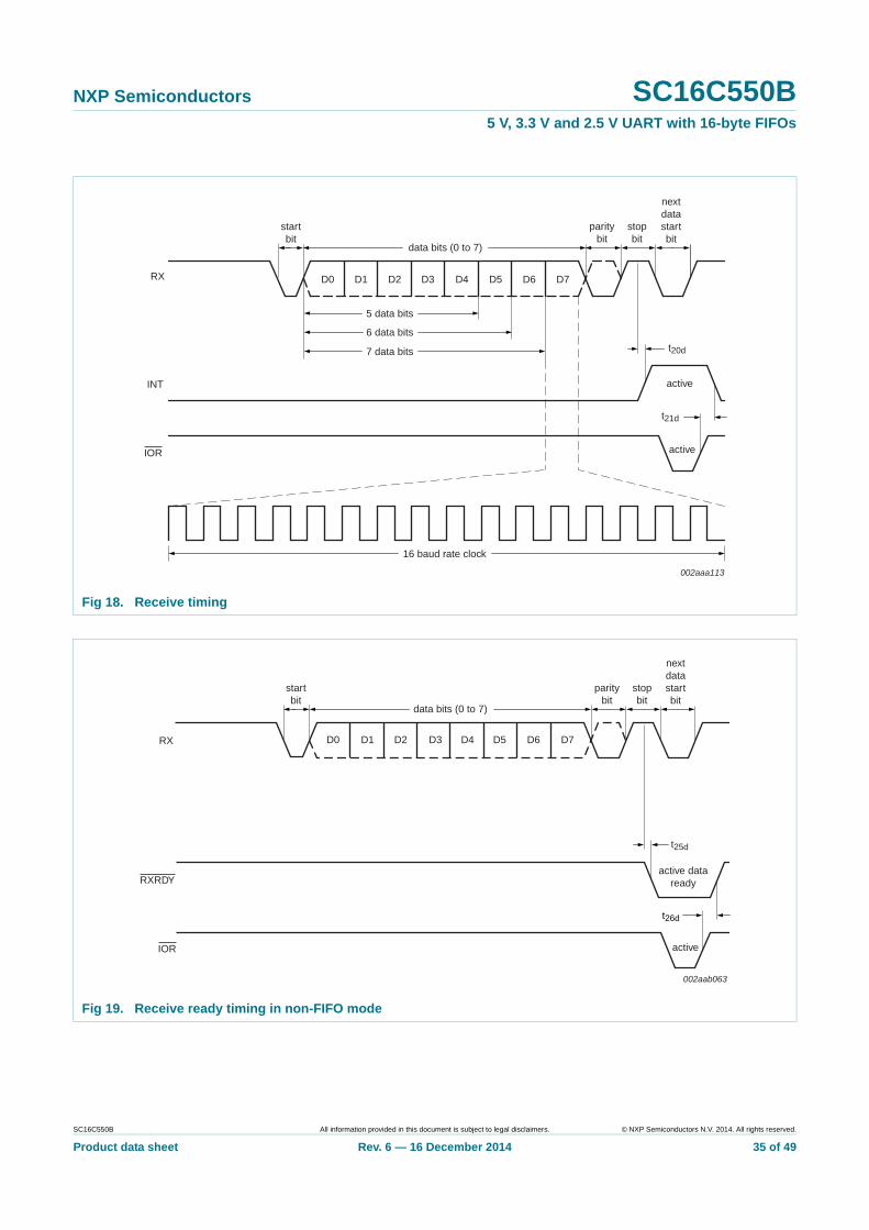
Fig 18. Receive timing
D0 D1 D2 D3 D4 D5 D6 D7
active
active
16 baud rate clock
002aaa113
RX
INT
IOR
t21d
t20d
5 data bits
6 data bits
7 data bits
stopbit
paritybit
startbit
data bits (0 to 7)
nextdatastartbit
Fig 19. Receive ready timing in non-FIFO mode
D0 D1 D2 D3 D4 D5 D6 D7
002aab063
nextdatastartbit
stopbit
paritybit
t25d
RX
RXRDY
IOR
active dataready
startbit
data bits (0 to 7)
active
t26d
SC16C550B All information provided in this document is subject to legal disclaimers. © NXP Semiconductors N.V. 2014. All rights reserved.
Product data sheet Rev. 6 — 16 December 2014 35 of 49

NXP Semiconductors SC16C550B5 V, 3.3 V and 2.5 V UART with 16-byte FIFOs
Fig 20. Receive ready timing in FIFO mode
D0 D1 D2 D3 D4 D5 D6 D7
002aab064
first byte thatreaches thetrigger level
stopbit
paritybit
t25d
RX
RXRDY
IOR
active dataready
startbit
data bits (0 to 7)
active
t26d
Fig 21. Transmit timing
activetransmitter ready
active
16 baud rate clock
002aaa116
t24d
INT
IOW active
D0 D1 D2 D3 D4 D5 D6 D7TX
5 data bits
6 data bits
7 data bits
stopbit
paritybit
startbit
data bits (0 to 7)
nextdatastartbit
t22dt23d
SC16C550B All information provided in this document is subject to legal disclaimers. © NXP Semiconductors N.V. 2014. All rights reserved.
Product data sheet Rev. 6 — 16 December 2014 36 of 49

NXP Semiconductors SC16C550B5 V, 3.3 V and 2.5 V UART with 16-byte FIFOs
Fig 22. Transmit ready timing in non-FIFO mode
D0 D1 D2 D3 D4 D5 D6 D7
002aaa580
startbit
t27d
TXRDY
IOW
data bits (0 to 7)
active
D0 to D7 byte #1t28d
transmitternot ready
activetransmitter ready
paritybit
stopbit
nextdatastartbit
TX
Fig 23. Transmit ready timing in FIFO mode (DMA mode ‘1’)
D0 D1 D2 D3 D4 D5 D6 D7
002aab061
stopbit
paritybit
t27d
TX
IOW
D0 to D7
startbit
data bits (0 to 7)
byte #16
TXRDY
t28d
FIFO full
active
5 data bits
6 data bits
7 data bits
SC16C550B All information provided in this document is subject to legal disclaimers. © NXP Semiconductors N.V. 2014. All rights reserved.
Product data sheet Rev. 6 — 16 December 2014 37 of 49
NXP Semiconductors SC16C550B5 V, 3.3 V and 2.5 V UART with 16-byte FIFOs
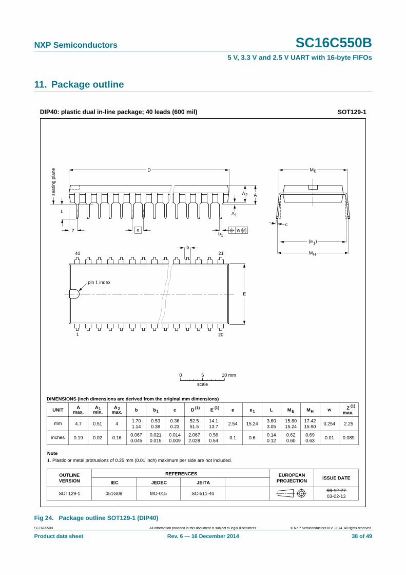
11. Package outline
Fig 24. Package outline SOT129-1 (DIP40)
UNIT Amax.
1 2 b1 c D E e MHL
REFERENCESOUTLINEVERSION
EUROPEANPROJECTION ISSUE DATE
IEC JEDEC JEITA
mm
inches
DIMENSIONS (inch dimensions are derived from the original mm dimensions)
SOT129-199-12-2703-02-13
A min.
A max. b Z
max.wMEe1
1.701.14
0.530.38
0.360.23
52.551.5
14.113.7
3.603.05
0.2542.54 15.2415.8015.24
17.4215.90
2.254.7 0.51 4
0.0670.045
0.0210.015
0.0140.009
2.0672.028
0.560.54
0.140.12
0.010.1 0.60.620.60
0.690.63
0.089 0.19 0.02 0.16
051G08 MO-015 SC-511-40
MH
c
(e )1
ME
A
L
seat
ing
plan
e
A1
w Mb1
e
D
A2
Z
40
1
21
20
b
E
pin 1 index
0 5 10 mm
scale
Note
1. Plastic or metal protrusions of 0.25 mm (0.01 inch) maximum per side are not included.
(1)(1)(1)
DIP40: plastic dual in-line package; 40 leads (600 mil) SOT129-1
SC16C550B All information provided in this document is subject to legal disclaimers. © NXP Semiconductors N.V. 2014. All rights reserved.
Product data sheet Rev. 6 — 16 December 2014 38 of 49
NXP Semiconductors SC16C550B5 V, 3.3 V and 2.5 V UART with 16-byte FIFOs
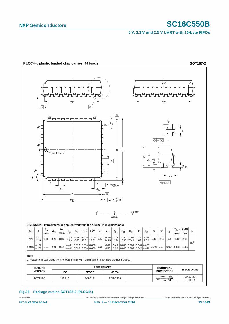
Fig 25. Package outline SOT187-2 (PLCC44)
UNIT AA1
min.
A4max.
bp e ywv β
REFERENCESOUTLINEVERSION
EUROPEANPROJECTION ISSUE DATE
IEC JEDEC JEITA
mm 4.574.19 0.51 3.05
0.530.33
0.0210.013
16.6616.51
1.2717.6517.40 2.16
45o0.18 0.10.18
DIMENSIONS (mm dimensions are derived from the original inch dimensions)
Note
1. Plastic or metal protrusions of 0.25 mm (0.01 inch) maximum per side are not included.
SOT187-2
D(1) E(1)
16.6616.51
HD HE
17.6517.40
ZD(1)
max.ZE
(1)
max.
2.16
b1
0.810.66
k
1.221.07
0.1800.165 0.02 0.12
A3
0.25
0.010.6560.650
0.050.6950.685 0.0850.007 0.0040.007
Lp
1.441.02
0.0570.040
0.6560.650
0.6950.685
eD eE
16.0014.99
0.630.59
16.0014.99
0.630.59 0.085
0.0320.026
0.0480.042
2939
44
1
6
7 17
28
18
40
detail X
(A )3
bp
w M
A1A
A4
Lp
b1
βk
Xy
e
E
B
DH
Ee
EH
v M B
D
ZD
A
ZE
e
v M A
pin 1 index
112E10 MS-018 EDR-7319
0 5 10 mm
scale
99-12-2701-11-14
inches
PLCC44: plastic leaded chip carrier; 44 leads SOT187-2
De
SC16C550B All information provided in this document is subject to legal disclaimers. © NXP Semiconductors N.V. 2014. All rights reserved.
Product data sheet Rev. 6 — 16 December 2014 39 of 49

NXP Semiconductors SC16C550B5 V, 3.3 V and 2.5 V UART with 16-byte FIFOs
Fig 26. Package outline SOT313-2 (LQFP48)
UNITA
max. A1 A2 A3 bp c E(1) e HE L Lp Zywv θ
REFERENCESOUTLINEVERSION
EUROPEANPROJECTION ISSUE DATE
IEC JEDEC JEITA
mm 1.6 0.200.05
1.451.35
0.250.270.17
0.180.12
7.16.9 0.5
9.158.85
0.950.55
70
o
o0.12 0.10.21
DIMENSIONS (mm are the original dimensions)
Note
1. Plastic or metal protrusions of 0.25 mm maximum per side are not included.
0.750.45
SOT313-2 MS-026136E0500-01-1903-02-25
D(1) (1)(1)
7.16.9
HD
9.158.85
EZ
0.950.55
D
bp
e
E
B
12
DH
bp
EH
v M B
D
ZD
A
ZE
e
v M A
1
48
37
36 25
24
13
θ
A1A
Lp
detail X
L
(A )3A2
X
y
c
w M
w M
0 2.5 5 mm
scale
pin 1 index
LQFP48: plastic low profile quad flat package; 48 leads; body 7 x 7 x 1.4 mm SOT313-2
SC16C550B All information provided in this document is subject to legal disclaimers. © NXP Semiconductors N.V. 2014. All rights reserved.
Product data sheet Rev. 6 — 16 December 2014 40 of 49

NXP Semiconductors SC16C550B5 V, 3.3 V and 2.5 V UART with 16-byte FIFOs
Fig 27. Package outline SOT617-1 (HVQFN32)
0.51
A1 EhbUNIT ye
0.2
c
REFERENCESOUTLINEVERSION
EUROPEANPROJECTION ISSUE DATE
IEC JEDEC JEITA
mm 5.14.9
Dh
3.252.95
y1
5.14.9
3.252.95
e1
3.5
e2
3.50.300.18
0.050.00
0.05 0.1
DIMENSIONS (mm are the original dimensions)
SOT617-1 MO-220- - - - - -
0.50.3
L
0.1
v
0.05
w
0 2.5 5 mm
scale
SOT617-1HVQFN32: plastic thermal enhanced very thin quad flat package; no leads;32 terminals; body 5 x 5 x 0.85 mm
A(1)
max.
AA1
c
detail X
yy1 Ce
L
Eh
Dh
e
e1
b
9 16
32 25
24
178
1
X
D
E
C
B A
e2
terminal 1index area
terminal 1index area
01-08-0802-10-18
1/2 e
1/2 e ACC
Bv M
w M
E(1)
Note
1. Plastic or metal protrusions of 0.075 mm maximum per side are not included.
D(1)
SC16C550B All information provided in this document is subject to legal disclaimers. © NXP Semiconductors N.V. 2014. All rights reserved.
Product data sheet Rev. 6 — 16 December 2014 41 of 49
NXP Semiconductors SC16C550B5 V, 3.3 V and 2.5 V UART with 16-byte FIFOs
12. Soldering of SMD packages
This text provides a very brief insight into a complex technology. A more in-depth account of soldering ICs can be found in Application Note AN10365 “Surface mount reflow soldering description”.
12.1 Introduction to soldering
Soldering is one of the most common methods through which packages are attached to Printed Circuit Boards (PCBs), to form electrical circuits. The soldered joint provides both the mechanical and the electrical connection. There is no single soldering method that is ideal for all IC packages. Wave soldering is often preferred when through-hole and Surface Mount Devices (SMDs) are mixed on one printed wiring board; however, it is not suitable for fine pitch SMDs. Reflow soldering is ideal for the small pitches and high densities that come with increased miniaturization.
12.2 Wave and reflow soldering
Wave soldering is a joining technology in which the joints are made by solder coming from a standing wave of liquid solder. The wave soldering process is suitable for the following:
• Through-hole components
• Leaded or leadless SMDs, which are glued to the surface of the printed circuit board
Not all SMDs can be wave soldered. Packages with solder balls, and some leadless packages which have solder lands underneath the body, cannot be wave soldered. Also, leaded SMDs with leads having a pitch smaller than ~0.6 mm cannot be wave soldered, due to an increased probability of bridging.
The reflow soldering process involves applying solder paste to a board, followed by component placement and exposure to a temperature profile. Leaded packages, packages with solder balls, and leadless packages are all reflow solderable.
Key characteristics in both wave and reflow soldering are:
• Board specifications, including the board finish, solder masks and vias
• Package footprints, including solder thieves and orientation
• The moisture sensitivity level of the packages
• Package placement
• Inspection and repair
• Lead-free soldering versus SnPb soldering
12.3 Wave soldering
Key characteristics in wave soldering are:
• Process issues, such as application of adhesive and flux, clinching of leads, board transport, the solder wave parameters, and the time during which components are exposed to the wave
• Solder bath specifications, including temperature and impurities
SC16C550B All information provided in this document is subject to legal disclaimers. © NXP Semiconductors N.V. 2014. All rights reserved.
Product data sheet Rev. 6 — 16 December 2014 42 of 49
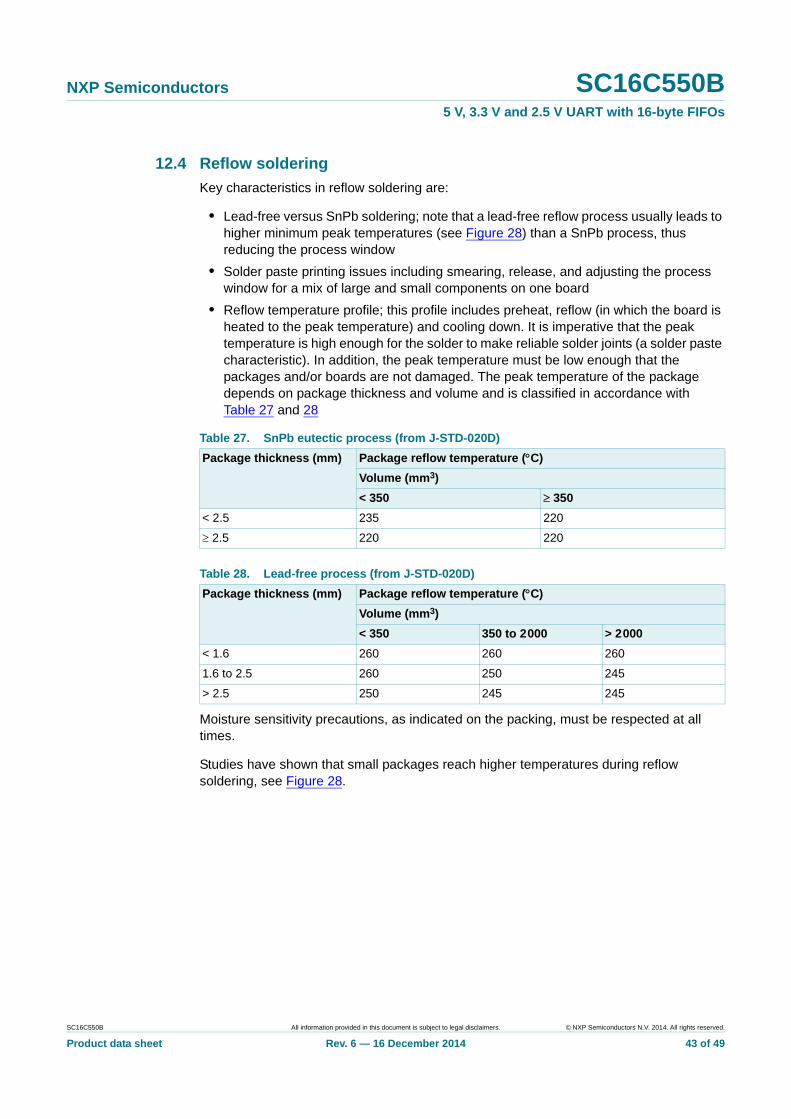
NXP Semiconductors SC16C550B5 V, 3.3 V and 2.5 V UART with 16-byte FIFOs
12.4 Reflow soldering
Key characteristics in reflow soldering are:
• Lead-free versus SnPb soldering; note that a lead-free reflow process usually leads to higher minimum peak temperatures (see Figure 28) than a SnPb process, thus reducing the process window
• Solder paste printing issues including smearing, release, and adjusting the process window for a mix of large and small components on one board
• Reflow temperature profile; this profile includes preheat, reflow (in which the board is heated to the peak temperature) and cooling down. It is imperative that the peak temperature is high enough for the solder to make reliable solder joints (a solder paste characteristic). In addition, the peak temperature must be low enough that the packages and/or boards are not damaged. The peak temperature of the package depends on package thickness and volume and is classified in accordance with Table 27 and 28
Moisture sensitivity precautions, as indicated on the packing, must be respected at all times.
Studies have shown that small packages reach higher temperatures during reflow soldering, see Figure 28.
Table 27. SnPb eutectic process (from J-STD-020D)
Package thickness (mm) Package reflow temperature (C)
Volume (mm3)
< 350 350
< 2.5 235 220
2.5 220 220
Table 28. Lead-free process (from J-STD-020D)
Package thickness (mm) Package reflow temperature (C)
Volume (mm3)
< 350 350 to 2000 > 2000
< 1.6 260 260 260
1.6 to 2.5 260 250 245
> 2.5 250 245 245
SC16C550B All information provided in this document is subject to legal disclaimers. © NXP Semiconductors N.V. 2014. All rights reserved.
Product data sheet Rev. 6 — 16 December 2014 43 of 49
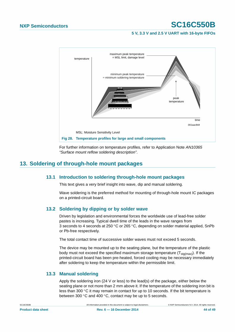
NXP Semiconductors SC16C550B5 V, 3.3 V and 2.5 V UART with 16-byte FIFOs
For further information on temperature profiles, refer to Application Note AN10365 “Surface mount reflow soldering description”.
13. Soldering of through-hole mount packages
13.1 Introduction to soldering through-hole mount packages
This text gives a very brief insight into wave, dip and manual soldering.
Wave soldering is the preferred method for mounting of through-hole mount IC packages on a printed-circuit board.
13.2 Soldering by dipping or by solder wave
Driven by legislation and environmental forces the worldwide use of lead-free solder pastes is increasing. Typical dwell time of the leads in the wave ranges from 3 seconds to 4 seconds at 250 C or 265 C, depending on solder material applied, SnPb or Pb-free respectively.
The total contact time of successive solder waves must not exceed 5 seconds.
The device may be mounted up to the seating plane, but the temperature of the plastic body must not exceed the specified maximum storage temperature (Tstg(max)). If the printed-circuit board has been pre-heated, forced cooling may be necessary immediately after soldering to keep the temperature within the permissible limit.
13.3 Manual soldering
Apply the soldering iron (24 V or less) to the lead(s) of the package, either below the seating plane or not more than 2 mm above it. If the temperature of the soldering iron bit is less than 300 C it may remain in contact for up to 10 seconds. If the bit temperature is between 300 C and 400 C, contact may be up to 5 seconds.
MSL: Moisture Sensitivity Level
Fig 28. Temperature profiles for large and small components
001aac844
temperature
time
minimum peak temperature= minimum soldering temperature
maximum peak temperature= MSL limit, damage level
peak temperature
SC16C550B All information provided in this document is subject to legal disclaimers. © NXP Semiconductors N.V. 2014. All rights reserved.
Product data sheet Rev. 6 — 16 December 2014 44 of 49
NXP Semiconductors SC16C550B5 V, 3.3 V and 2.5 V UART with 16-byte FIFOs
13.4 Package related soldering information
[1] For SDIP packages, the longitudinal axis must be parallel to the transport direction of the printed-circuit board.
[2] For PMFP packages hot bar soldering or manual soldering is suitable.
14. Abbreviations
Table 29. Suitability of through-hole mount IC packages for dipping and wave soldering
Package Soldering method
Dipping Wave
CPGA, HCPGA - suitable
DBS, DIP, HDIP, RDBS, SDIP, SIL suitable suitable[1]
PMFP[2] - not suitable
Table 30. Abbreviations
Acronym Description
CMOS Complementary Metal-Oxide Semiconductor
CPU Central Processing Unit
DLL Divisor Latch LSB
DLM Divisor Latch MSB
DMA Direct Memory Access
FIFO First-In, First-Out
ISDN Integrated Service Digital Network
LSB Least Significant Bit
MSB Most Significant Bit
TTL Transistor-Transistor Logic
UART Universal Asynchronous Receiver and Transmitter
SC16C550B All information provided in this document is subject to legal disclaimers. © NXP Semiconductors N.V. 2014. All rights reserved.
Product data sheet Rev. 6 — 16 December 2014 45 of 49

NXP Semiconductors SC16C550B5 V, 3.3 V and 2.5 V UART with 16-byte FIFOs
15. Revision history
Table 31. Revision history
Document ID Release date Data sheet status Change notice Supersedes
SC16C550B_6 20141216 Product data sheet - SC16C550B_5
Modifications: • Table 9 “SC16C550B internal registers”: changed MCR bit 3 from “OUT2” to “OUT2, INT enable”; updated Table note 4.
SC16C550B_5 20081001 Product data sheet - SC16C550B_4
SC16C550B_4 20070316 Product data sheet - SC16C550B_3
SC16C550B_3 (9397 750 14986)
20050620 Product data sheet - SC16C550B-02
SC16C550B-02 (9397 750 14446)
20041214 Product data - SC16C550B-01
SC16C550B-01 (9397 750 11967)
20040326 Product data - -
SC16C550B All information provided in this document is subject to legal disclaimers. © NXP Semiconductors N.V. 2014. All rights reserved.
Product data sheet Rev. 6 — 16 December 2014 46 of 49

NXP Semiconductors SC16C550B5 V, 3.3 V and 2.5 V UART with 16-byte FIFOs
16. Legal information
16.1 Data sheet status
[1] Please consult the most recently issued document before initiating or completing a design.
[2] The term ‘short data sheet’ is explained in section “Definitions”.
[3] The product status of device(s) described in this document may have changed since this document was published and may differ in case of multiple devices. The latest product status information is available on the Internet at URL http://www.nxp.com.
16.2 Definitions
Draft — The document is a draft version only. The content is still under internal review and subject to formal approval, which may result in modifications or additions. NXP Semiconductors does not give any representations or warranties as to the accuracy or completeness of information included herein and shall have no liability for the consequences of use of such information.
Short data sheet — A short data sheet is an extract from a full data sheet with the same product type number(s) and title. A short data sheet is intended for quick reference only and should not be relied upon to contain detailed and full information. For detailed and full information see the relevant full data sheet, which is available on request via the local NXP Semiconductors sales office. In case of any inconsistency or conflict with the short data sheet, the full data sheet shall prevail.
Product specification — The information and data provided in a Product data sheet shall define the specification of the product as agreed between NXP Semiconductors and its customer, unless NXP Semiconductors and customer have explicitly agreed otherwise in writing. In no event however, shall an agreement be valid in which the NXP Semiconductors product is deemed to offer functions and qualities beyond those described in the Product data sheet.
16.3 Disclaimers
Limited warranty and liability — Information in this document is believed to be accurate and reliable. However, NXP Semiconductors does not give any representations or warranties, expressed or implied, as to the accuracy or completeness of such information and shall have no liability for the consequences of use of such information. NXP Semiconductors takes no responsibility for the content in this document if provided by an information source outside of NXP Semiconductors.
In no event shall NXP Semiconductors be liable for any indirect, incidental, punitive, special or consequential damages (including - without limitation - lost profits, lost savings, business interruption, costs related to the removal or replacement of any products or rework charges) whether or not such damages are based on tort (including negligence), warranty, breach of contract or any other legal theory.
Notwithstanding any damages that customer might incur for any reason whatsoever, NXP Semiconductors’ aggregate and cumulative liability towards customer for the products described herein shall be limited in accordance with the Terms and conditions of commercial sale of NXP Semiconductors.
Right to make changes — NXP Semiconductors reserves the right to make changes to information published in this document, including without limitation specifications and product descriptions, at any time and without notice. This document supersedes and replaces all information supplied prior to the publication hereof.
Suitability for use — NXP Semiconductors products are not designed, authorized or warranted to be suitable for use in life support, life-critical or safety-critical systems or equipment, nor in applications where failure or malfunction of an NXP Semiconductors product can reasonably be expected to result in personal injury, death or severe property or environmental damage. NXP Semiconductors and its suppliers accept no liability for inclusion and/or use of NXP Semiconductors products in such equipment or applications and therefore such inclusion and/or use is at the customer’s own risk.
Applications — Applications that are described herein for any of these products are for illustrative purposes only. NXP Semiconductors makes no representation or warranty that such applications will be suitable for the specified use without further testing or modification.
Customers are responsible for the design and operation of their applications and products using NXP Semiconductors products, and NXP Semiconductors accepts no liability for any assistance with applications or customer product design. It is customer’s sole responsibility to determine whether the NXP Semiconductors product is suitable and fit for the customer’s applications and products planned, as well as for the planned application and use of customer’s third party customer(s). Customers should provide appropriate design and operating safeguards to minimize the risks associated with their applications and products.
NXP Semiconductors does not accept any liability related to any default, damage, costs or problem which is based on any weakness or default in the customer’s applications or products, or the application or use by customer’s third party customer(s). Customer is responsible for doing all necessary testing for the customer’s applications and products using NXP Semiconductors products in order to avoid a default of the applications and the products or of the application or use by customer’s third party customer(s). NXP does not accept any liability in this respect.
Limiting values — Stress above one or more limiting values (as defined in the Absolute Maximum Ratings System of IEC 60134) will cause permanent damage to the device. Limiting values are stress ratings only and (proper) operation of the device at these or any other conditions above those given in the Recommended operating conditions section (if present) or the Characteristics sections of this document is not warranted. Constant or repeated exposure to limiting values will permanently and irreversibly affect the quality and reliability of the device.
Terms and conditions of commercial sale — NXP Semiconductors products are sold subject to the general terms and conditions of commercial sale, as published at http://www.nxp.com/profile/terms, unless otherwise agreed in a valid written individual agreement. In case an individual agreement is concluded only the terms and conditions of the respective agreement shall apply. NXP Semiconductors hereby expressly objects to applying the customer’s general terms and conditions with regard to the purchase of NXP Semiconductors products by customer.
No offer to sell or license — Nothing in this document may be interpreted or construed as an offer to sell products that is open for acceptance or the grant, conveyance or implication of any license under any copyrights, patents or other industrial or intellectual property rights.
Document status[1][2] Product status[3] Definition
Objective [short] data sheet Development This document contains data from the objective specification for product development.
Preliminary [short] data sheet Qualification This document contains data from the preliminary specification.
Product [short] data sheet Production This document contains the product specification.
SC16C550B All information provided in this document is subject to legal disclaimers. © NXP Semiconductors N.V. 2014. All rights reserved.
Product data sheet Rev. 6 — 16 December 2014 47 of 49

NXP Semiconductors SC16C550B5 V, 3.3 V and 2.5 V UART with 16-byte FIFOs
Export control — This document as well as the item(s) described herein may be subject to export control regulations. Export might require a prior authorization from competent authorities.
Non-automotive qualified products — Unless this data sheet expressly states that this specific NXP Semiconductors product is automotive qualified, the product is not suitable for automotive use. It is neither qualified nor tested in accordance with automotive testing or application requirements. NXP Semiconductors accepts no liability for inclusion and/or use of non-automotive qualified products in automotive equipment or applications.
In the event that customer uses the product for design-in and use in automotive applications to automotive specifications and standards, customer (a) shall use the product without NXP Semiconductors’ warranty of the product for such automotive applications, use and specifications, and (b) whenever customer uses the product for automotive applications beyond
NXP Semiconductors’ specifications such use shall be solely at customer’s own risk, and (c) customer fully indemnifies NXP Semiconductors for any liability, damages or failed product claims resulting from customer design and use of the product for automotive applications beyond NXP Semiconductors’ standard warranty and NXP Semiconductors’ product specifications.
Translations — A non-English (translated) version of a document is for reference only. The English version shall prevail in case of any discrepancy between the translated and English versions.
16.4 TrademarksNotice: All referenced brands, product names, service names and trademarks are the property of their respective owners.
17. Contact information
For more information, please visit: http://www.nxp.com
For sales office addresses, please send an email to: [email protected]
SC16C550B All information provided in this document is subject to legal disclaimers. © NXP Semiconductors N.V. 2014. All rights reserved.
Product data sheet Rev. 6 — 16 December 2014 48 of 49

NXP Semiconductors SC16C550B5 V, 3.3 V and 2.5 V UART with 16-byte FIFOs
18. Contents
1 General description . . . . . . . . . . . . . . . . . . . . . . 1
2 Features and benefits . . . . . . . . . . . . . . . . . . . . 1
3 Ordering information. . . . . . . . . . . . . . . . . . . . . 2
4 Block diagram . . . . . . . . . . . . . . . . . . . . . . . . . . 3
5 Pinning information. . . . . . . . . . . . . . . . . . . . . . 45.1 Pinning . . . . . . . . . . . . . . . . . . . . . . . . . . . . . . . 45.2 Pin description . . . . . . . . . . . . . . . . . . . . . . . . . 6
6 Functional description . . . . . . . . . . . . . . . . . . . 96.1 Internal registers. . . . . . . . . . . . . . . . . . . . . . . 106.2 FIFO operation . . . . . . . . . . . . . . . . . . . . . . . . 106.3 Autoflow control . . . . . . . . . . . . . . . . . . . . . . . 116.3.1 Auto-RTS . . . . . . . . . . . . . . . . . . . . . . . . . . . . 116.3.2 Auto-CTS . . . . . . . . . . . . . . . . . . . . . . . . . . . . 116.3.3 Enabling autoflow control and auto-CTS . . . . 126.3.4 Auto-CTS and auto-RTS functional timing . . . 126.4 Hardware/software and time-out interrupts. . . 136.5 Programmable baud rate generator . . . . . . . . 146.6 DMA operation . . . . . . . . . . . . . . . . . . . . . . . . 156.7 Loopback mode . . . . . . . . . . . . . . . . . . . . . . . 16
7 Register descriptions . . . . . . . . . . . . . . . . . . . 187.1 Transmit Holding Register (THR) and
Receive Holding Register (RHR) . . . . . . . . . . 197.2 Interrupt Enable Register (IER) . . . . . . . . . . . 197.2.1 IER versus Receive FIFO interrupt mode
operation. . . . . . . . . . . . . . . . . . . . . . . . . . . . . 207.2.2 IER versus Receive/Transmit FIFO polled
mode operation. . . . . . . . . . . . . . . . . . . . . . . . 207.3 FIFO Control Register (FCR) . . . . . . . . . . . . . 207.3.1 DMA mode . . . . . . . . . . . . . . . . . . . . . . . . . . . 207.3.1.1 Mode 0 (FCR bit 3 = 0) . . . . . . . . . . . . . . . . . . 207.3.1.2 Mode 1 (FCR bit 3 = 1) . . . . . . . . . . . . . . . . . . 207.3.2 FIFO mode . . . . . . . . . . . . . . . . . . . . . . . . . . . 217.4 Interrupt Status Register (ISR) . . . . . . . . . . . . 227.5 Line Control Register (LCR) . . . . . . . . . . . . . . 237.6 Modem Control Register (MCR) . . . . . . . . . . . 257.7 Line Status Register (LSR) . . . . . . . . . . . . . . . 267.8 Modem Status Register (MSR) . . . . . . . . . . . . 277.9 Scratchpad Register (SPR) . . . . . . . . . . . . . . 287.10 SC16C550B external reset conditions . . . . . . 28
8 Limiting values. . . . . . . . . . . . . . . . . . . . . . . . . 28
9 Static characteristics. . . . . . . . . . . . . . . . . . . . 29
10 Dynamic characteristics . . . . . . . . . . . . . . . . . 3010.1 Timing diagrams . . . . . . . . . . . . . . . . . . . . . . . 32
11 Package outline . . . . . . . . . . . . . . . . . . . . . . . . 38
12 Soldering of SMD packages . . . . . . . . . . . . . . 4212.1 Introduction to soldering . . . . . . . . . . . . . . . . . 42
12.2 Wave and reflow soldering. . . . . . . . . . . . . . . 4212.3 Wave soldering . . . . . . . . . . . . . . . . . . . . . . . 4212.4 Reflow soldering . . . . . . . . . . . . . . . . . . . . . . 43
13 Soldering of through-hole mount packages. 4413.1 Introduction to soldering through-hole mount
packages . . . . . . . . . . . . . . . . . . . . . . . . . . . . 4413.2 Soldering by dipping or by solder wave . . . . . 4413.3 Manual soldering . . . . . . . . . . . . . . . . . . . . . . 4413.4 Package related soldering information. . . . . . 45
14 Abbreviations . . . . . . . . . . . . . . . . . . . . . . . . . 45
15 Revision history . . . . . . . . . . . . . . . . . . . . . . . 46
16 Legal information . . . . . . . . . . . . . . . . . . . . . . 4716.1 Data sheet status . . . . . . . . . . . . . . . . . . . . . . 4716.2 Definitions . . . . . . . . . . . . . . . . . . . . . . . . . . . 4716.3 Disclaimers . . . . . . . . . . . . . . . . . . . . . . . . . . 4716.4 Trademarks . . . . . . . . . . . . . . . . . . . . . . . . . . 48
17 Contact information . . . . . . . . . . . . . . . . . . . . 48
18 Contents. . . . . . . . . . . . . . . . . . . . . . . . . . . . . . 49
© NXP Semiconductors N.V. 2014. All rights reserved.
For more information, please visit: http://www.nxp.comFor sales office addresses, please send an email to: [email protected]
Date of release: 16 December 2014
Document identifier: SC16C550B
Please be aware that important notices concerning this document and the product(s)described herein, have been included in section ‘Legal information’.