Embed Size (px)
Citation preview
1. Civil Status Paolo BONDAVALLI Birth Date : 18/09/69 Mantua (Italy) Address : 110 résidence des eaux vives, 91120 Palaiseau tel: ++33 01.69.41.58.83 (Travail) ou 01.60.10.92.69 (home) email : [email protected]; [email protected] Position : Head of the nanomaterial team , joint team UMR137 CNRS/Thales Member of the joint team Ecole Polytechnique/Thales, NANOCARB Lab. Site Web : http://www.trt.thalesgroup.com/ump-cnrs-thales/presentation_uk.htm Spoken Languages : � French : bilingual � Italian : mother tongue � English : fluent � Espagnol : beginner.
2. Academic awards � 3 Mai 2011 HDR Paris Sud : Réseaux aléatoires de nanotubes de carbone : modèles théoriques et réalisation de transistors pour la détection de gaz (“Carbon Nanotubes besed network : theoretical mode ls and fabrication of transistors for gas sensing applications”) Philippe Bergonzo (CEA LIST) Marc Chatelet (Ecole Polytechnique) Philippe Dollfus (Paris Sud) Bernard Drévillon (Ecole polytechnique) Henry G. Happy (IEMN) Rapporteur
Adrian M. Ionescu (EPFL) Rapporteur
Annick Loiseau (ONERA) Rapporteur
� January 2000 - Novembre 1996-: PhD, specialisation « Integrated electronics devices », INSA of Lyon, Laboratoire de Physique de la Matière (LPM) in collaboration with Ecole Centrale de Lyon, Laboratoire d'Electronique, Optoélectronique et Microsystèmes (LEOM) , now INL. Mention Très Honorable (31/01/00). Title : « Microsystèmes Optomécaniques à base d`InP pour l`analyse de gaz ». (“InP based Optomechanical systems for gas sensing ap plications”) Short summary : Study on the optical and mechanical modeling of Microsystems for gas sensing applications. These Microsystems were composed of Fabry-Pérot cavities for selecting absorption wavelengths for gas sensing application. This research work was achieved in collaboration with SCHLUMBERGER et THOMSON-CSF Key words : MOEMS (Micro-Opto-Mechanical Systems), III-V materials, Sensors, Optical and mechanical design, Tests. Oral defence : 31/01/2000 Jury : G.Guillot (Insa de Lyon)
M.Garrigues (Ecole Centrale Lyon) M. DeLabachelerie (Institut FEMTO-ST, Besançon) J-L.Robert (Université. Montpellier II) M.Ingrain (EDF GDF)
P.Mottier (CEA LETI) � 1995 : Laurea in State solid physics (level DEA + Master) Parma University (Italy). Oral defense 20/11/95. Title : « Etude de l’absorption optique fondamentale de couches de GaSb et AlGaSb » (« Study of the optical fundamental absorption of GaSb and AlGaSb layers ») Short summary : Study of the fundamental optical absorption as a function of the temperature variation and of the Al content in the ternary compound. Key Words : III-V materials, Tests. Optical properties of semiconductor compounds 3. Professional experience/employment (Career) � 2011-2009 Head of the nanomaterial team ( NANOMAT) joint team Thales/CNRS (Director F. Nguyen-Van Dau, Scientific director A.Fert) UMR 137. Research project coordination (CEE and French Research Agency projects) :
ANR-NANOSENSOFIN 2007-2010: new concept of gas sensing devices based on CNTFETs (Field effect carbon nanotubes based transistors) Partners : Thales (prime), Ecole Polytechnique CEA-LITEN, Sofileta, ANR-CAPTEX 2010-2012 : integrated nano-sensors for peroxyde sensing. Parteners : Thales (prime), CEA-LITEN, Ecole Polytechnique, Iness Strasbourg, Université de Metz, CEA-DAM, Novapack, NEDEX NMP FP7 HINTS 2011 –2014 : (University of Bologna, prime) Organic spintronics NMP FP7 GRAPHOL 2011-2015 : (University of Cambridge, prime) Graphene based applications (spintronics, RF transistors, sensors…)
Research topics : Graphene, Carbon nanotubes, spintronics, new nanomaterials for energy, energy storage (one patent); nanomaterial deposition using a new kind of air-brush method (one patent). � 2009-2004 : In charge of the development of nanomaechnolgy ba sed devices (sensors) NANOCARB lab. (joint team Ecole Polytechnique/Thales) Direction de projets ANR :
ANR-NANOBIOSENSOR 2006-2009 (Biosensing using nanowires) Parteners : Ecole Polytecnique (LPICM) (Coordinateur), Thales, CEA- Ecole Polytecnique (BIOC), LAAS ANR-NANOSENSOFIN 2007-2010 : (mentioned above).
Participation in different research projects : FP6 CANDICE (new architectures for CNT based transistors), FP7 NINIVE (CNT based antennas), FP7 NANOPACK (CNT based management). Topics : gas sensing (one patent), biosensing using nanowires, thermal management (two patents). � 2004-2001 : R&D Engineer at Microtec 3D lab at THALES RESEARCH AND TECHNOLOGY, Orsay. Participation in different research projects : FP6 ARHMS (phase shifters using MEMS array), ESA-MEMS² (MEMS for space applications), RNRT MOUSTIC (1999-2002, gas sensing using MOEMS), FP6 ARRESAT (2003-2005, phase shifters using MEMS).

Research topics : Microtechnologies (RF micro-switches), MEMS DESIGN. Micro-packaging. � 2001-2000 R&D Engineer at Microtec 3D lab at THALES laser di odes, Orsay Project direction on micro-packaging of power laser diodes : FP5 NIMED (lasers for printing). 4. Teaching experiences � 2012 Seminars on Innovation case studies : Ecole Central e de Paris
6 hours . This seminar consists in explaining how we deal with innovation at Thales Research and technologies. Some case studies are presented.
� 2011-2007 Practical and Seminars on « Microsystems-MOEMS » at
“Ecole Supérieure d’Optique” (5 th year). This practical consists of 12 sessions of two hours each. These sessions deal with mechanical and optical simulation of MOEMS. Two sessions, of 3 hours each, are devoted to a seminar on MOEMS (history, applications, physics, market forecast). . I have written and developed all the didactical ma terial : theory and experimental.
� 2011–2007 Practical on « Carbon Nanotubes based sensors » at “Ecole Polytechnique” (3 rd year). This practical consists of 6 sessions of 4 hours each. These sessions deal with the fabrication of CNTFETs using CNT mats. I have written and developed all the teaching aid.
� 1999-1998, Practical on Optic Fibers at INSA of Lyo n (5 th year)
This practical consists of 20 sessions of 2 hours each. Properties of light transport in optic fibers. I have written and developed all the teaching aids.
� 1999 –1998 -1997, Practical at INSA of Lyon (5 th year) on :
� Low pressure instrumentation � Mass spectrometry � Liquid flow measurement � Liquid phase chromatography
Three years 52 hours/year for three years (80 stude nts each year). I have written and developed all the teaching aids.
5. Administrative responsibilities � European Expert FP6/FP7 :
o Call People Marie-Curie Actions (FP7-PEOPLE-IXF) Physics panel – IEF, IIF and OIF schemes.
o Call People Marie-Curie Actions (FP7-PEOPLE-CIG) o Call People Marie-Curie Actions (FP7-PEOPLE-IAPP) o Call People Marie-Curie Actions (FP7-PEOPLE-IRESES). o FP7 NMP o FP7 ICT
� Expert for the National French Agency (PNANO et CSOG). � Expert EDA (European Defence Agency), � Reviewer
o Institute of Physics (IOP Nanotechnology, Journal of Physics: Condensed Matter, Journal of Physics D : Applied Physics, Measurement Science and Technology, Journal of Micromechanics and Microengineering, Smart Materials and Structures)
o Elsevier (Sensors and Actuators A and B), o Institute of Electrical and Electronics Engineers (IEEE-sensors,
Transactions en nanotechnology), o The European Physical Journal - Applied Physics” (EPJAP ). o Taylor and Francis (Journal of experimental Nanoscience, Analytical
letters), o Bentham (Recent Patents on Electrical Engineering) o Electrochemical Systems (ECS).
� Member of l’‘‘European Technology Platform for Advanced Materials and Technologies” (EUMAT).
� MRS member � IEEE member � French Society of Physics member � French Physics Society Member
European Excellence Networks � Member of the European Excellence Network GOSPEL (General Olfaction
and Sensing Projects on a European Level) (FP7) � Member of the European Excellence Network NANOTOLIFE (FP7) (Biology
and nanotechnology covergence) � Member of the European Excellence Network USC MEMS PACKAGING :
Workshop organisation (site d’Orsay). � Member of the European Excellence Network «Design for Micro & Nano
Manufacture (NoE PATENT-DfMM)» : workshop organization (Orsay). � Member of the European Excellence Network AMICOM (Advanced MEMS
for RF and millimeterwave communications)
European project involvement � ESPRIT MOEMS, European project (MOEMS for WDM) 1996-1999 � RNRT MOUSTIC, French research agency project (MOEMS for WDM) 2000-
2002 � NIMED FP5 STREP(laser diodes for printing applications) 2000-2002 � ARRESAT FP6 Strep 2003-2005 (phase shifters using MEMS)
� ARHMS FP6 STREP (MEMS RF for phase shifters) 2004-2006 � MEMS² (ESA) (MEMS RF Packaging) 2002-2005 � CANDICE FP6 STREP (CNTFETs with new kind of lateral architecture) 2005-
2007 � ANR NANOBIOSENSOR, French Research Agency (Biosensing) 2006-2008 � NINIVE FP6 STREP (CNT based antennas for bio-applications) 2006-2008 � ANR NANOSENSOFIN, French Research Agency (prime) 2007-2010 (gas
sensing using CNTs) � NANOPACK IP FP7 (thermal properties of CNTs) 2008-2011 � TECHNOTUBE IP FP7 2009-2012 � ANR CAPTEX, French Research Agency (prime) (Explosive sensing using
CNTFETs) 2010-2012 � HINTS (FP7 NMP) organic spintronics applications 2011-2014 � GRAFOL (FP7 NMP) Graphene applications (spintronique, sensing, HF…)
Recent Patents on micro-nanotechnology Three patents submitted this year : � NOUVELLE METHODES POUR LA REALISATION DE DEPOTS
MODULABLES ET REPRODUCTIBLES DE NANOMATERIAUX SUR DES GRANDES SURFACES ET POTENTIELLES APPLICATIONS, P.Bondavalli , L .Gorintin, P.Legagneux, 2010
� STRUCTURES HYBRIDES A BASE DE NANOTUBES DE CARBONE ET DE
GRAPHENE/GRAPHITE REALISEES PAR METHODE DE SPRAY DYNAMIQUE POUR L’AUGMENTATION DE LA PUISSANCE DELIVREE PAR UNE SUPERCAPACITES, P.Bondavalli , L .Gorintin, P.Legagneux, 2011
� FORET DE RESEAUX ALEATOIRE DE NANOTUBES/NANOFILS
RECOUVERTS D’UNE COUCHE DE NANODIAMANT POUR LRD ELECTRODES DES SUPERCAPACITES P.Legagneux, P.Bondavalli , P.Legagneux, JP Mazelliers, P.Bergonzo 2011
Three patents : � ELECTROSTATIC ACTUATION MICROSWITCH INCLUDING NANOTUBES
FOR HEAT MANAGEMENT AND RELATED PRODUCTION METHOD, P.Bondavalli , P.Legagneux, WO2009071498 (2009)
� ELECTRONIC DEVICE, HAS THERMAL RADIATOR DISSIPATING HEAT
RELEASED BY ELECTRONIC COMPONENTS, AND THERMAL INTERFACE ASSURING CONTACT BETWEEN COMPONENTS AND THERMAL RADIATOR AND INCLUDING FILM PROVIDED WITH CARBON NANOTUBES , P.Bondavalli , P.Legagneux, FR2924861 (2008)
� CONDUCTIVE NANOTUBE OR NANOWIRE FET TRANSISTOR NETWORK
AND CORRESPONDING ELECTRONIC DEVICE, FOR DETECTING
ANALYTES, P.Bondavalli , P.Legagneux, D.Pribat, P.Lebarny, J.Nagle, WO2006128828 (2006)
E-repository � RESEAU DE CAPTEURS A BASSE CONSOMMATION ENERGETIQUE
POUR LE MONITORAGE DE L’ENVIRONNEMENT, P.Bondavalli , G.Feugnet, e-repository 2010
� INTERFACES THERMIQUES À FORTE CONDUCTIVITÉ THERMIQUE
CONTENANT DES NANOTUBES DE CARBONE ALIGNÉS PAR DIÉLECTROPHORÈSE, P.Bondavalli , S.Demosutier, P.LeBarny, P.Legagneux, e-repository 2009
� RÉSEAU DE TRANSISTORS À BASE DE NANOTUBES DE CARBONE À
DIAMÈTRE VARIABLE OU DE NANOFILS ISSUS DE DIFFÉRENTS MATÉRIAUX SEMI-CONDUCTEURS POUR LA DÉTECTION D’ANALYTES, P.Bondavalli , P.Legagneux, D.Pribat, e-repository 2009
7. People Management 2000 : Thales Laser Diodes Trainees management.
2012-2004 : Thales Research and Technology (ex Laboratoire Central de Recherche de THOMSON CSF) : Trainees Management (level): Final year Ecole Centrale de Lyon 2nd year Ecole Polytechnique Final year Université Paris Sud Management of three PhD thesis students: � Gaelle Lehoucq 2006- 2009 (march 2010) : Fabrication of biosensors using silicon nanowires based transistors (DGA Thesis) PhD Direction : Didier Pribat, Ecole Polytecnique and Paolo Bondavalli
� Louis Gorintin 2009 – 2011 (November 2011) Fabrication of carbon nanotubes based transistors for gas sensing applications PhD direction : Didier Pribat, Ecole Polytecnique and Paolo Bondava lli � Marta Galbiati 2011 – 2014 Organic spintronics PhD direction : Fréderic Petroff, Paris Sud and Paolo Bondavalli
People management full table
50% Louis Gorintin, PhD Thesis CIFRE from Ecole Centrale de Lyon (2009-2012) (10 proceedings, 3 papers, 2 patents, 1 book chapter) 50% Gaelle Lehoucq, PhD Thesis DGA from Ecole Centrale de Lille (2007-2010) (2 proceedings, 1 paper) 100% Adrian Balan, third year Ecole Polytechnique (2007), 1 paper (Price for the best trainee report of Ecole Polytechnique) 100% Soline Diesbach, third year Ecole Supérieure de Chimie, Physique, Electronique de Lyon (2006) 100% Vincent Dupuis, final year training, Ecole Centrale de Lyon (2006), 1 paper (1 e-repository) 100% Sebastien Nazeer, final year training (DEA), Paris Sud, Paris 11 (2007), 1 paper 100% Louis Gorintin, DEA, Ecole Centrale Lyon (2009), 2 proceedings 100% Daniel Garcia, 2nd year, ESPEO (2000) 50% Jean Marc Cornier, final year training ESPEO (2000) Award : Adrian Balan, third year Ecole Polytechnique (2007) Best trainee report of Ecole Polytechnique

8. Major achievements 1996- 2000 : During my PhD thesis at INSA of Lyon I have studied the opto-mechanical modelling of MOEMS for gas sensing appli cations and WDM. This study has been done in collaboration of EcolE Centrale de Lyon. This work has been performed in the frame of the ESPRIT project “MOEMS inP” . The other partners were : KTH, Ericsson, Alcatel. From this study an opto-mechanical model has been set up (see paper on JMC, 1999).
� Optical modelling of multi-layers systems based on III-V semiconductors.
� Modelling and design of MOEMS � Optical characterisation
2000- 2001 : I have been hired by Thales Laser Diodes in May 2000. I was in charge of the research and development of new power laser diodes. The work consisted in defining packaging, test set-up, to suggest new kin ds of products and to develop them. I was in charge of several research projects. For example, NIMED (FP5) project dealt with the fabrication of a laser diodes stacks for printing applications. In this case, the main issues were the thermal management and the packaging. A prototype has been fabricated and delivered to the end-user.
� Specific test bench set up � Packaging, Thermal modelling � Research grant direction � People management
2001- 2004 : I moved to Thales Research and Technology where I was in charg e of the technological development of MEMS RF and packaging issues at the Microtech 3D lab.Actually I thought that my previous experience was too focussed on development and not on real research issues. In this new position, I had to identify the best materials for the fabrication and packaging of the MEMS. I also worked on the design of MEMS for bio-medical applications (membrane for sonar). I was in charge of several European project (ESA, ARRESAT, ARHMS, MEMS²);
� Technological step definition � Packaging � Material optimization � People and contract management
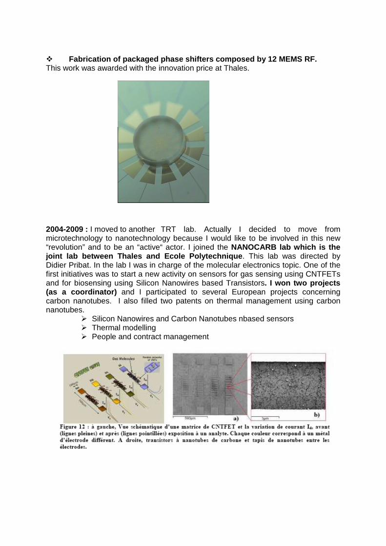
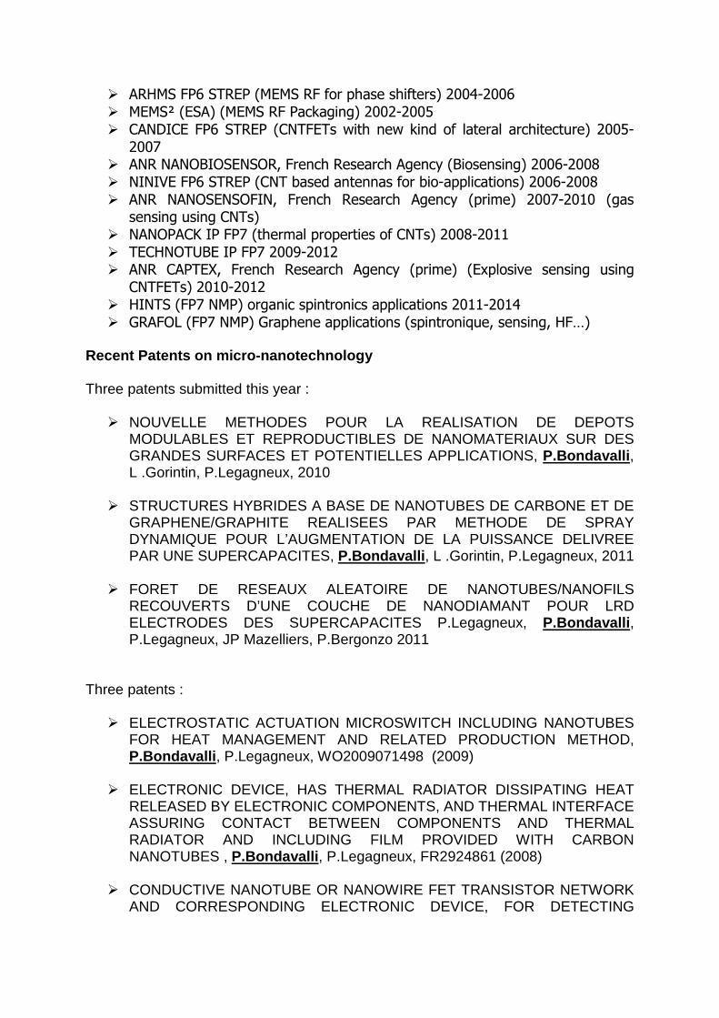
� Fabrication of packaged phase shifters composed by 12 MEMS RF. This work was awarded with the innovation price at Thales. 2004-2009 : I moved to another TRT lab. Actually I decided to move from microtechnology to nanotechnology because I would like to be involved in this new “revolution” and to be an “active“ actor. I joined the NANOCARB lab which is the joint lab between Thales and Ecole Polytechnique . This lab was directed by Didier Pribat. In the lab I was in charge of the molecular electronics topic. One of the first initiatives was to start a new activity on sensors for gas sensing using CNTFETs and for biosensing using Silicon Nanowires based Transistors. I won two projects (as a coordinator) and I participated to several European projects concerning carbon nanotubes. I also filled two patents on thermal management using carbon nanotubes.
� Silicon Nanowires and Carbon Nanotubes nbased sensors � Thermal modelling � People and contract management
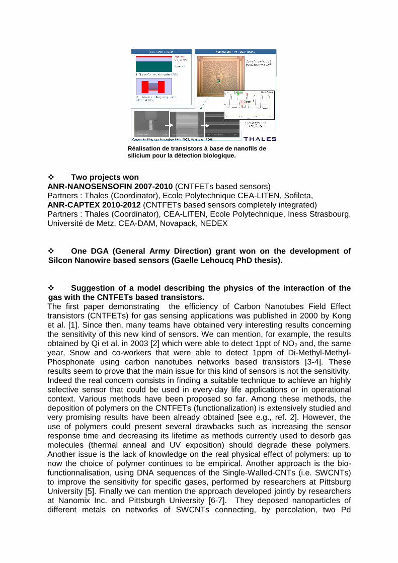
Réalisation de transistors à base de nanofils de silicium pour la détection biologique.
� Two projects won ANR-NANOSENSOFIN 2007-2010 (CNTFETs based sensors) Partners : Thales (Coordinator), Ecole Polytechnique CEA-LITEN, Sofileta, ANR-CAPTEX 2010-2012 (CNTFETs based sensors completely integrated) Partners : Thales (Coordinator), CEA-LITEN, Ecole Polytechnique, Iness Strasbourg, Université de Metz, CEA-DAM, Novapack, NEDEX � One DGA (General Army Direction) grant won on the d evelopment of Silcon Nanowire based sensors (Gaelle Lehoucq PhD t hesis). � Suggestion of a model describing the physics of the interaction of the gas with the CNTFETs based transistors. The first paper demonstrating the efficiency of Carbon Nanotubes Field Effect transistors (CNTFETs) for gas sensing applications was published in 2000 by Kong et al. [1]. Since then, many teams have obtained very interesting results concerning the sensitivity of this new kind of sensors. We can mention, for example, the results obtained by Qi et al. in 2003 [2] which were able to detect 1ppt of NO2 and, the same year, Snow and co-workers that were able to detect 1ppm of Di-Methyl-Methyl-Phosphonate using carbon nanotubes networks based transistors [3-4]. These results seem to prove that the main issue for this kind of sensors is not the sensitivity. Indeed the real concern consists in finding a suitable technique to achieve an highly selective sensor that could be used in every-day life applications or in operational context. Various methods have been proposed so far. Among these methods, the deposition of polymers on the CNTFETs (functionalization) is extensively studied and very promising results have been already obtained [see e.g., ref. 2]. However, the use of polymers could present several drawbacks such as increasing the sensor response time and decreasing its lifetime as methods currently used to desorb gas molecules (thermal anneal and UV exposition) should degrade these polymers. Another issue is the lack of knowledge on the real physical effect of polymers: up to now the choice of polymer continues to be empirical. Another approach is the bio-functionnalisation, using DNA sequences of the Single-Walled-CNTs (i.e. SWCNTs) to improve the sensitivity for specific gases, performed by researchers at Pittsburg University [5]. Finally we can mention the approach developed jointly by researchers at Nanomix Inc. and Pittsburgh University [6-7]. They deposed nanoparticles of different metals on networks of SWCNTs connecting, by percolation, two Pd

electrodes (i.g. “metal decoration”). Therefore they fabricated an array of CNTFETs each one characterized by a different metal “decoration”. They exposed this array to several gases (NO, H2, CO, CH4, H2S, NO2, NH3) and they observed a specific change of the transfer characteristics of each transistor as a function of the nature of the nanoparticles and of the gas. These results made researchers think that large array of “metal-decorated” CNTFETs could be used in order to recognize univocally the gases identifying their electronic fingerprinting. All the approaches that we have presented appear to be very interesting from a scientific point of view but the technological steps for the fabrication of the sensors (e.g. polymer/bio-fonctionnalisation or metal decoration) are quite complex and the their industrial exploitation has not been achieved yet. Our approach for solving the selectivity problem, is to achieve a sensor comprising an array of SWCNT-based transistors where each transistor will be fabricated using different metals as source/drain electrodes. Considering that no cheap and rapid method, up to now, exists for separating semiconductor from metallic specimens, we decided to use SWCNT mats as transistor channel. The principal advantages are two. Firstly the use of SWCNT mats instead of individual SWNTs (facilitating methodology) results in percolation networks with a better overall electrical control of the system. Secondly, using dynamic spray-gun technique (patented by Thales) we can achieve uniform and highly controlled SWCNT densities which allows us to obtain CNTFETs with highly reproducible electrical characteristics [8-9]. Moreover, this technique allows us to fabricate large array of sensors with a method very simple, rapid, totally compatible with existing CMOS technology and so suitable for industrial exploitation and relatively low-cost. We have chosen to diversify the metals electrodes in order to exploit the different effect of the interaction of the gas with the metal/SWCNTs junction on the Schottky barrier. As a consequence after gas exposure the Fermi level alignment between metal and CNT at the contact, will change and therefore the characteristics of the Schottky barrier at the junction. In fact we cannot talk about a “real” Schottky barrier but in our case because we do not deal with a junction with an intimate contact (like classical Schottky barrier between semiconductor and metal where the Fermi Level is pinned by interface defects as explained by F.Leonard et al. in 2000 [10]). In our case we have a “non-intimate” contact because the SWCNT is simply deposited on the metal without annealing. This model was firstly suggested by T.Yamada of the Ames Research Center in 2004 [11-12] for Au/SWCNT contacts, generalized by P.Bondavalli et al. [13] to all the metal/ SCWNT junctions and, for network based CNTFETs, improved by F.Peng et al. in 2009 [14]. In this contribution we will demonstrate that, after being exposed to different gases (NO2, NH3 and DMMP) at concentration from 10ppb to 10ppm, each transistor will be influenced in a very peculiar way : this influence on the barrier is strictly related to the interaction between a specific gas and a specific metal/CNT junction [15]. Indeed, the gas will change the metal work function and so the junction electrical behaviour. This is not possible in traditional for semiconductor/metal junction because the Fermi level is pinned by, as told previously, interface defects. Using this method, we will be able to demonstrate that each gas will be “fingerprinted” and so unambiguously identified. [1]. Kong J, Franklyn NR , Zhou C, Chapline MG, Peng S, Cho K, Dai H 2000 Science 287 622-625 [2] Qi P, Vermesh O, Grecu M, Javey A, Wang Q and Dai H, 2003 Nano Lett. 3 347-351 [3]. Novak JP, Snow E S, Houser E J, Park D, Stepnowski JL, McGill RA 2003 Applied Phys. Lett. 83 19 4026-4028 [4]. Snow ES, Novak JP, Lay MD,. Houser EH, Perkins FK and Campbell PM 2004 J. Vac. Sci. Technol. B 22 4 1990-1994 [5] Staii C, Johnson AT, Chen M, Gelperin A 2005 Nano Lett. 5 9 1774–1778. [6]. Starr A, Joshi V, Skarupo S, Thomas D, Gabriel J-C.P 2006 J. Phys. Chem. B 110 21014–21020 [7] Kauffmann D.R., Starr A., 2007 Nano Lett. 7 7 1863–1868. [8] Bondavalli P, Gorintin L, Legagneux P, Simonato JP, Cailler L 2011 MRS Proc. 1283 mrsf10-1283-
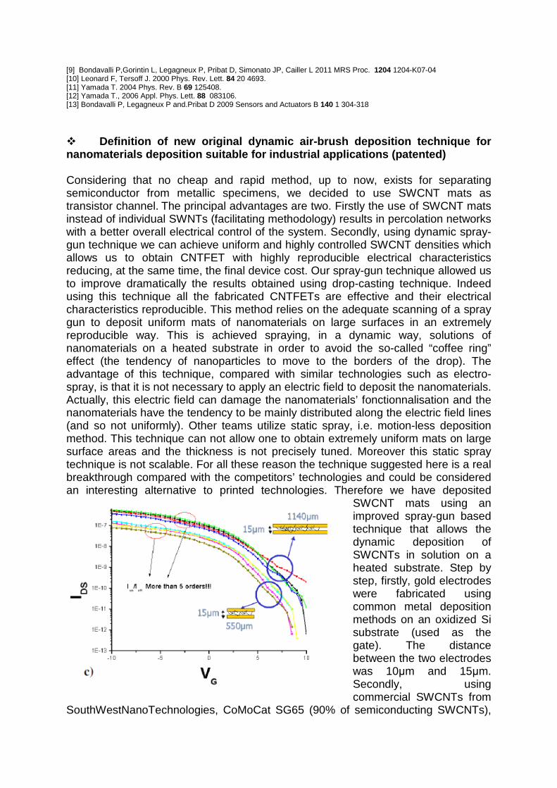
[9] Bondavalli P,Gorintin L, Legagneux P, Pribat D, Simonato JP, Cailler L 2011 MRS Proc. 1204 1204-K07-04 [10] Leonard F, Tersoff J. 2000 Phys. Rev. Lett. 84 20 4693. [11] Yamada T. 2004 Phys. Rev. B 69 125408. [12] Yamada T., 2006 Appl. Phys. Lett. 88 083106. [13] Bondavalli P, Legagneux P and.Pribat D 2009 Sensors and Actuators B 140 1 304-318 � Definition of new original dynamic air-brush deposi tion technique for nanomaterials deposition suitable for industrial ap plications (patented) Considering that no cheap and rapid method, up to now, exists for separating semiconductor from metallic specimens, we decided to use SWCNT mats as transistor channel. The principal advantages are two. Firstly the use of SWCNT mats instead of individual SWNTs (facilitating methodology) results in percolation networks with a better overall electrical control of the system. Secondly, using dynamic spray-gun technique we can achieve uniform and highly controlled SWCNT densities which allows us to obtain CNTFET with highly reproducible electrical characteristics reducing, at the same time, the final device cost. Our spray-gun technique allowed us to improve dramatically the results obtained using drop-casting technique. Indeed using this technique all the fabricated CNTFETs are effective and their electrical characteristics reproducible. This method relies on the adequate scanning of a spray gun to deposit uniform mats of nanomaterials on large surfaces in an extremely reproducible way. This is achieved spraying, in a dynamic way, solutions of nanomaterials on a heated substrate in order to avoid the so-called “coffee ring” effect (the tendency of nanoparticles to move to the borders of the drop). The advantage of this technique, compared with similar technologies such as electro-spray, is that it is not necessary to apply an electric field to deposit the nanomaterials. Actually, this electric field can damage the nanomaterials’ fonctionnalisation and the nanomaterials have the tendency to be mainly distributed along the electric field lines (and so not uniformly). Other teams utilize static spray, i.e. motion-less deposition method. This technique can not allow one to obtain extremely uniform mats on large surface areas and the thickness is not precisely tuned. Moreover this static spray technique is not scalable. For all these reason the technique suggested here is a real breakthrough compared with the competitors’ technologies and could be considered an interesting alternative to printed technologies. Therefore we have deposited
SWCNT mats using an improved spray-gun based technique that allows the dynamic deposition of SWCNTs in solution on a heated substrate. Step by step, firstly, gold electrodes were fabricated using common metal deposition methods on an oxidized Si substrate (used as the gate). The distance between the two electrodes was 10µm and 15µm. Secondly, using commercial SWCNTs from
SouthWestNanoTechnologies, CoMoCat SG65 (90% of semiconducting SWCNTs),

we have achieved, after a sonication and a centrifugation step, stabilized solutions using N-Methyl-pyrrolidone (NMP) as solvent. These solutions are deposited on the substrate, where the electrodes have been fabricated, using a spray-gun. The substrate was heated at a temperature higher than 202°C (evaporation point for NMP) in order to evaporate instantaneously the solvent droplets hitting the substrate : in this way drop will instantaneously “collapse”. This last detail allows us to dramatically improve the uniformity of the SWCNTs mats preventing the so-called “coffee ring effect” (deposition of SWCNTs on the borders of the drops evaporated at room temperature) achieving mats with state of the art reproducible characteristics. spray-gun technique has been optimized only recently. Some of the transfer characteristics of the transistors achieved using this technique shown in figure 1, and reported in figure 2, show that we can achieve CNTFETs with high Log(Ion)/ Log(Ioff) current ratio (~5/6). These results are at the state of the art for SWCNTs mat based transistors. Moreover these results are reproducible and demonstrate the great potential for industrial application of this technique. � Thermal management of power MEMS for HF application s using CNTs, reduction of the influence of Hot Spots Two patents filled during the particicpation to the project NANOPACK which dealt with thermal management using nanoparticles.
9. Scientific Papers International reviews and book chapter (in red submitted) Evidence of gas selective sensing using CNTFETs fabricated using a air-brush deposition technique with different metals as electrodes, P.Bondavalli, F.Longnos, L.Gorintin, G.Lehoucq, Gilles Feugnet submitted to Nanotechnology 2011 Highly sensitive pH sensing using sensors composed by large array of parallel Silicon Nanowires, G.Lehoucq, P.Bondavalli, et al. submitted to Sensors and Actuators B: Chemical 2011 Carbon nanotubes based supercapacitors : state of the art and critical review since 1997. P. Bondavalli, JP Schnell, L. Gorintin, submitted to Journal of Physical Chemistry C 2011 All-printed infrared sensor based on multi-walled carbon nanotubes, Gohier, A. Dhar L. Gorintin P. Bondavalli , Y. Bonnassieux, C.S. Cojocaru, Appl. Phys. Lett. 98, 063103 (2011) CNTs for gas sensing (book chapter), P. Bondavalli , L. Gorintin and P. Legagneux Applications of Carbon Nanotubes, Pan Stanford Series, Ed. Zhang Qing, Pan Stanford Publishing Pte Ltd (published 31th december 2011) Carbon Nanotubes based Transistors composed of Single-Walled Carbon Nanotubes mats as Gas Sensors : a Review, P.Bondavalli , Comptes-Rendus de l'Académie des Sciences (Elsevier), September 2010 CNTFETs based gas sensors : patent review, P. Bondavalli, Recent Patents on Electrical Engineering, 3 (2010) CNTFET based gas sensors : State of the art and critical review, P.Bondavalli , P.Legagneux and D.Pribat, Sensors and Actuators B, Volume 140, Issue 1, Pages 304-318, (2009) Sub ppm gas sensing using CNTFET based array, P.Bondavalli , P.Legagneux and D.Pribat, Journal of the Korean Physical Society, Vol. 54, n. 1, pp. 510-513, (2009) Gas fingerprinting using Carbon Nanotubes transistors arrays, P.Bondavalli , P.Legagneux and D.Pribat, Journal of Experimental Nanoscience, 3(04), pp. 347 – 356, 2008 Carbon Nanotubes and Semiconductor Nanowires for Active Matrix Backplanes, D. Pribat, C. S. Cojocaru, M. Gowtham and L. Eude, P.Bondavalli , Pierre Legagneux, Journal of the Society for Information Display , Volume 15, Issue 8, pp. 595-600, August 2007 Capteurs de gaz à base de nanotubes de carbone : une nouvelle génération de capteurs nanométriques, P.Bondavalli , P.Legagneux and D.Pribat, REE, avril 2007
Influence of the involuntary underetching on the mechanical properties of tunable Fabry-Pérot filters for optical communications, P.Bondavalli et al. Journal of Microelectromechanical Systems, Vol.10,n 2, pp. 298-301, June 2001 Opto-mechanical design of InP-based Fabry-Pérot filters for gas analysis, P.Bondavalli et al., Sensors and Actuators A, Vol.94 , pp. 136-141, 2001 Proceedings (with review committee) Highly selective CNTFET based sensors using metal diversification methods (Proceedings Paper) P. Bondavalli ; L. Gorintin; F. Longnos; G. Feugnet Proceedings Vol. 8101, 81010A (San Diego 2011) New dynamic air-brush technique for SWCNTs deposition : application to electronics and gas sensing, P.Bondavalli , L.Gorintin, P.Legagneux, J-P. Simonato, L.Cailler, MRS Proceedings (2011), 1283 : mrsf10-1283-b01-06 CNTFET Gas Sensors using SWCNT Mats : Method for Low-cost Fabrication, Solution to Improve Selectivity, Influence of Humidity (and Methods to Reduce it), Experimental Results Using Interfering Agents, P.Bondavalli , L.Gorintin, P.Legagneux, D.Pribat, J-P. Simonato, L.Cailler, MRS Proceedings (2010) 1204, 1204-K07-04 Large-scale Production of Selective Gas Sensors Based on Carbon Nanotube Mats Transistors, Louis Gorintin, P.Bondavalli , Pierre Legagneux, Marc Chatelet, MRS Proceedings (2010) 1253, 1253-K08-02 Large Surface Reproducible CNTFETs Obtained Using Automatic Air-brush Machine, Paolo Bondavalli , Louis Gorintin, Proceedings of ITC10, Hyogo (26-28 January), Japan (2010) Inkjet-printed Carbon Nanotube Field-Effect Transistor using Nafion-based Dispersion on Glass Substrates, Anirban DHAR, Louis GORINTIN, Yvan BONNASSIEUX, Laurent BARATON, Costel Sorin COJOCARU, Paolo Bondavalli , Didier PRIBAT, Proceedings of ITC10, Hyogo (26-28 January), Japan (2010) Test and Modeling of the Electronic Behavior of Carbon Nanotubes High Performances Transistors obtained using Air-Brush Deposition Technique. P.Bondavalli , L.Gorintin, P.Legagneux, D.Pribat. Proceedings of the Eurosensors XXIII conference (Lausanne 6-9 September 2009 ), Procedia Chemistry, 2009 High performances CNTFET achieved using CNT networks for selective gas sensing, L.Gorintin , P.Bondavalli, P.Legagneux, D.Pribat, Proceedings of SPIE, San Diego (US), 2-6 Août 2009 Highly selective sensing of DMMP and NH3 using CNTFET array based gas sensors obtained using Spray-gun technique and fabricated with different metal electrodes to achieve gas electronic fingerprinting, P. Bondavalli , L.Gorintin, P.Legagneux and D.Pribat, Proceedings of Nanotech 2009, Houston (US), 3-7 May 2009
CNTFET gas sensors for security applications, P. Bondavalli , L.Gorintin, P.Legagneux and D.Pribat, Proceedings of ITC 09, Ecole Polytechnique, 5-6 Mars Palaiseau 2009 Preliminary Measurements of Selective sensing of DMMP and NH3 using CNTFET array based gas sensors fabricated using metal diversified electrodes for electronic fingerprinting, P. Bondavalli , P.Legagneux and D.Pribat, Mater. Res. Soc. (MRS) Symp. Proc. vol. 1081, P14-02, 2008 Sub ppm gas sensing using CNTFET based array, P. Bondavalli , P.Legagneux and D.Pribat, Proceedings of ITC 08, Seoul (South Korea) 2008 Carbon Nanotubes based sensor for gas fingerprinting, P. Bondavalli , P.Legagneux and D.Pribat, Proceedings of Nanotech 2007, Santa Clara (US), 20-24 May 2007 Packaging of MEMS arrays for microwaves applications, P.Bondavalli , T.Dean, A.Ziaei, Proceedings of Eurosensors X, Rome (Italy), 13-15 September 2004 Optical and mechanical design of an InP based tunable detector for gas sensing applications, P.Bondavalli , T. Benyattou, M. Garrigues, J.L.Leclerc, P.Regreny, K.Sun, P.Viktorovich, S.Cortial, X.Hugon, C.Pautet, Proceedings of SPIE, vol.3878, pp.174-184, (1999) International conferences and workshops
Highly selective CNTFET based sensors using metal diversification methods, P. Bondavalli ; L. Gorintin; F. Longnos; G. Feugnet, Spie 2011 San Diego, Invited Speaker A review of Carbon Based Supercapacitors, P.Bondavalli , Spie 2011 San Diego A review of Carbon Based Supercapacitors, P.Bondavalli , 1st Korean-French Seminar on Nanomaterials for Energy (SONATE) 6-8 Mars 2011, Invited Speaker A review of carbon based supercapacitors P. Bondavalli , , X-KHU 8th Common Workshop, Ecole Polytechnique, Palaiseau, Mars 1st 2011, Invited speaker New dynamic air-brush technique for SWCNTs deposition : application to electronics and gas sensing, P.Bondavalli , L.Gorintin, P.Legagneux, J-P. Simonato, L.Cailler, MRS Fall Meeting, Boston 27 novembre, 3 decembre 2010 Large Surface Reproducible CNTFETs Obtained Using Automatic Air-brush Machine, P.Bondavalli , L.Gorintin, P.Legagneux, JP Simonato, L.Cailler, TNT(Trends in Nanotechnologies)10, 6-9 septembre 2010 (oral) Gas sensors, A World of Nanotubes: Opto-Electronic Applications of Carbon Nanotubes, P. Bondavalli , ONERA scientific days (6-8 Avril 2010), Invited speaker
Large Surface Reproducible CNTFETs Obtained Using Automatic Air-brush Machine, Paolo Bondavalli , Louis Gorintin, ITC10, Hyogo (26-28 January), Japan CNTFET Gas Sensors using SWCNT Mats : Method for Low-cost Fabrication, Solution to Improve Selectivity, Influence of Humidity (and Methods to Reduce it), Experimental Results Using Interfering Agents, P.Bondavalli , L.Gorintin, P.Legagneux, D.Pribat, J-P. Simonato, L.Cailler, MRS09 Fall Meeting Boston 30 November, 3 December 2009 Large Area Deposition of Uniform CNT mats Using Scanning Air-Brush Gun P.Bondavalli, L.Gorintin, P.Legagneux, D.Pribat, TNT09 (Barcelona 7-10 September 2009) (Poster) Test and Modeling of the Electronic Behavior of Carbon Nanotubes High Performances Transistors obtained using Air-Brush Deposition Technique. P.Bondavalli , L.Gorintin, P.Legagneux, D.Pribat. Proceedings of the Eurosensors XXIII conference (Lausanne 6-9 September 2009 ), (Poster) High performances CNTFET achieved using CNT networks for selective gas sensing, L.Gorintin, P.Bondavalli , P.Legagneux, D.Pribat, SPIE (Nanoscience and Nanoengineering), San Diego (US), 3-6 August 2009 Highly selective sensing of DMMP and NH3 using CNTFET array based gas sensors obtained using Spray-gun technique and fabricated with different metal electrodes to achieve gas electronic fingerprinting, P. Bondavalli , L.Gorintin, P.Legagneux and D.Pribat, Nanotech 2009 , Houston (US), 3-7 May 2009 CNTFET gas sensors for security applications, P. Bondavalli , L.Gorintin, P.Legagneux and D.Pribat, ITC 09, Ecole Polytechnique, 5-6 Mars Palaiseau 2009 High performances CNTFET obtained using spray-gun deposition technique : analysis and considerations, P. Bondavalli , L.Gorintin, P.Legagneux and D.Pribat, X-KHU 6th Common Workshop, Ecole Polytechnique, Palaiseau, February 2nd 2009, Invited speaker Parallel Functionalized Silicon Microwires and Nanowires fabricated by top-down approach for Label-free Biosensing applications, G. Lehoucq, L. Mugherli, P. Bondavalli , M. Fromant, P. Plateau, S. Blanquet, P. Legagneux, D. Pribat, MRS Fall Meeting, Boston (US), 2008 (Poster) Utilization of carbon nanotubes for gas detection and quantification : state of the art and critical review, P.Bondavalli , MSIN08 at NT08, Montpellier 28 June 2008, Invited Speaker CNTFETs obtained using CNT uniform mats for gas sensing applications, P. Bondavalli , L. Gorintin, P. Legagneux and D. Pribat, NT08 Montpellier 29 June 4 July 2008 (Poster) Selective Sensing of DMMP and NH3 Using CNTFET Array Based Gas Sensors Fabricated Using Metal Diversified Electrodes for Electronic Fingerprinting. P.
Bondavalli , P. Legagneux and D. Pribat, MRS Spring Meeting 2008 , San Francisco (EU), 24-28 March 2008 Sub ppm gas sensing using CNTFET based array, P. Bondavalli , P. Legagneux and D. Pribat, ITC 08, Seoul (South Korea) 2008 (Poster) Sub ppm gas sensing using CNTFET based array, , P. Bondavalli, P.Legagneux and D.Pribat, X-KHU 6th Common Workshop , Seoul (South Korea) January 23rd 2008, Invited speaker Carbon Nanotubes based sensor for gas fingerprinting, P. Bondavalli , P. Legagneux and D. Pribat, Nanotech 2007 , Santa Clara (EU), 20-24 May 2007 Gas fingerprinting using carbon nanotubes transistors : a new concept, P. Bondavalli , P. Legagneux and D. Pribat, X-KHU 5th Common Workshop , Ecole Polytechnique, 22-23 January 2007, Invited speaker New concept of carbon nanotubes transistors matrix based sensor using metal contact diversification for highly selective gas imprinting, P. Bondavalli , P. Legagneux and D. Pribat, MRS Fall Meeting, Boston 2006 (EU), 27 November-1 December 2006 CNT and Si NW based NBC sensors, P. Bondavalli , P. Legagneux, D. Pribat, X-KHU 4th Common Workshop , Kyung Hee University, Seoul (South Korea), 12-13 January 2006, Invited speaker Packaging of MEMS arrays for microwaves applications, Eurosensors, P. Bondavalli , T. Dean, A. Ziaei, Rome (Italy), 13-15 September 2004 (Poster) Design, simulation, fabrication, and packaging of microwave RF switch, A. Ziaei, T.Dean, P. Bondavalli , Smart Structures , 2004 Optical and mechanical design of an InP based tunable detector for gas sensing applications, P. Bondavalli and al, Micromachining and Microfabrication, SPIE conference, Santa Clara (EU), 19-21 September 1999 Etudes optiques de filtres de Fabry-Pérot accordables en longueur d'onde à base d'InP pour le démultiplexage optique, P. Bondavalli , R. Ledantec, T. Benyattou, G. Guillot et al., MADICA 98 , Monastir 9-11 novembre 1998 National conferences Nouvelle technique de dépôt pour la réalisation de capteurs sélectifs à base de CNTFETs, P. Bondavalli , Workshop Interdisciplinaire sur la Sécurité Globale (WISG) , UTT (France), 25-26 January 2011 (Poster). Projet NANOSENSOFIN, P.Bondavalli, L.Gorintin, 8-10 novembre 2010, J3N Lille (Poster)
Projet CAPTEX, P. Bondavalli , Workshop Interdisciplinaire sur la Sécurité Globale (WISG) 2010, UTT (France), 27-28 January 2009 (Poster). Transistors à tapis de nanotubes et applications à la detection selective de gaz, L.Gorintin, P. Bondavalli , Convention de Physique TRT, 5/11/09 Microsensors based on carbon nanotubes for gas electronic fingerprinting, L.Gorintin, P.Bondavalli , 21-23 October, J3N Toulouse (Poster) Top-down Nanowire Field-Effect Transistors for real-time biological detection, G.Lehoucq, S. Xavier, M. Fromant, P. Bondavalli , P. Legagneux, GDR Nanofils 09 , Autran, Juin, 30, July, 3 (Oral and poster) CNTFET based sensors : a new generation of sensors, P. Bondavalli , P.Legagneux and D.Pribat, Proceedings of “Workshop Interdisciplinaire sur la Sécurité Globale (WISG) 2009, UTT (France), 27-28 January 2009. Des nouveaux capteurs nanometriques a base de nanotubes de carbone et nanofils de silicium pour la detection chimique et biologique, P. Bondavalli , Workshop Interdisciplinaire sur la Sécurité Globale (WISG) 2009, UTT (France), 27-28 January 2009 (Poster). CNT for gas sensing, P. Bondavalli , Journées de Palaiseau, Thales Research and Technology, Palaiseau, 16 December 2008, Invited Speaker CNTFET gas sensors and SiNw based bio-sensors, P. Bondavalli , G.Lehoucq, L.Gorintin, P. Legagneux and D. Pribat, Convention de Physique TRT, 14/11/08, Invited Speaker Biocapteurs à base de nanofils de silicium, G. Lehoucq, P. Bondavalli , P. Legagneux, L. Mugherli, L.Baraton, L. Eude, M. Fromant, D. Pribat, “Doctoriales 2008” of the Ecole Polytechnique, Fréjus, France, sept. 2008 (Poster) Biosensors based on silicon nanowires, G. Lehoucq, P. Bondavalli , P. Legagneux, L. Mugherli, L.Baraton, L. Eude, M. Fromant, D. Pribat, the Summer School on Semiconductor Nanowires (organization : GDR Nanofils), Roscoff, France, 10-15/06/2008 (Poster) Détecteurs de gas à base de nanotubes de carbone, P. Bondavalli, P. Legagneux and D. Pribat, Journée CAPTEO, Ecole-Polytechnique 11/01/08, Invited Speaker Nanobiosensors based on silicon nanowires, G. Lehoucq, L. Mugherli, L. Eude, S. Charlot, M. Fromant, P. Bondavalli , P. Plateau, S. Blanquet, P. Legagneux, A.M. Gué, D. Pribat, 27/09/07 J3N Porte de Versailles (Poster) Carbon nanotubes and nanowires based sensors for BC detection, P. Bondavalli , P. Legagneux, Workshop on Components and Technologies for Defense & Security, Paris, 7 November 2006 (Poster)
Capteurs de gaz à base de transistors à nanotubes de carbone, P. Bondavalli , ASPROM : Nanotechnologies et Nanosciences, Paris 23 Mai 2006, Invited speaker Commutateur MEMS pour la réalisation d’Antenne à Réseau Réflecteur à faibles pertes, A. Ziaei, T. Dean, P. Bondavalli , Journées Nationales Microondes, 21-22-23 May 2003, Lille Conception d'un micro-capteur de gaz é base d'un filtre Fabry-Pérot accordable sur InP, P. Bondavalli , T. Benyattou, M. Garrigues, P. Viktorovitch, JMNO 99, Egat 5-7 January (Poster)