Embed Size (px)
Citation preview
0. Introduction
1. Reminder:E-Dynamics in homogenous media and at interfaces
2. Photonic Crystals2.1 Introduction2.2 1D Photonic Crystals2.3 2D and 3D Photonic Crystals2.4 Numerical Methods2.5 Fabrication2.6 Non-linear optics and Photonic Crystals
2.6.1 Non-linear optics2.6.2 Phase-matching2.6.3 Band-structure tuning2.6.4 All-optical switching
2.7 Quantumoptics2.8 Chiral Photonic Crystals2.9 Quasicrystals2.10 Photonic Crystal Fibers – „Holey“ Fibers
3. Metamaterials and Plasmonics3.1 Introduction3.2 Background3.2 Fabrication3.3 Experiments
Non-linear optics
Non-linear reaction of a material to an incident EM-field
=
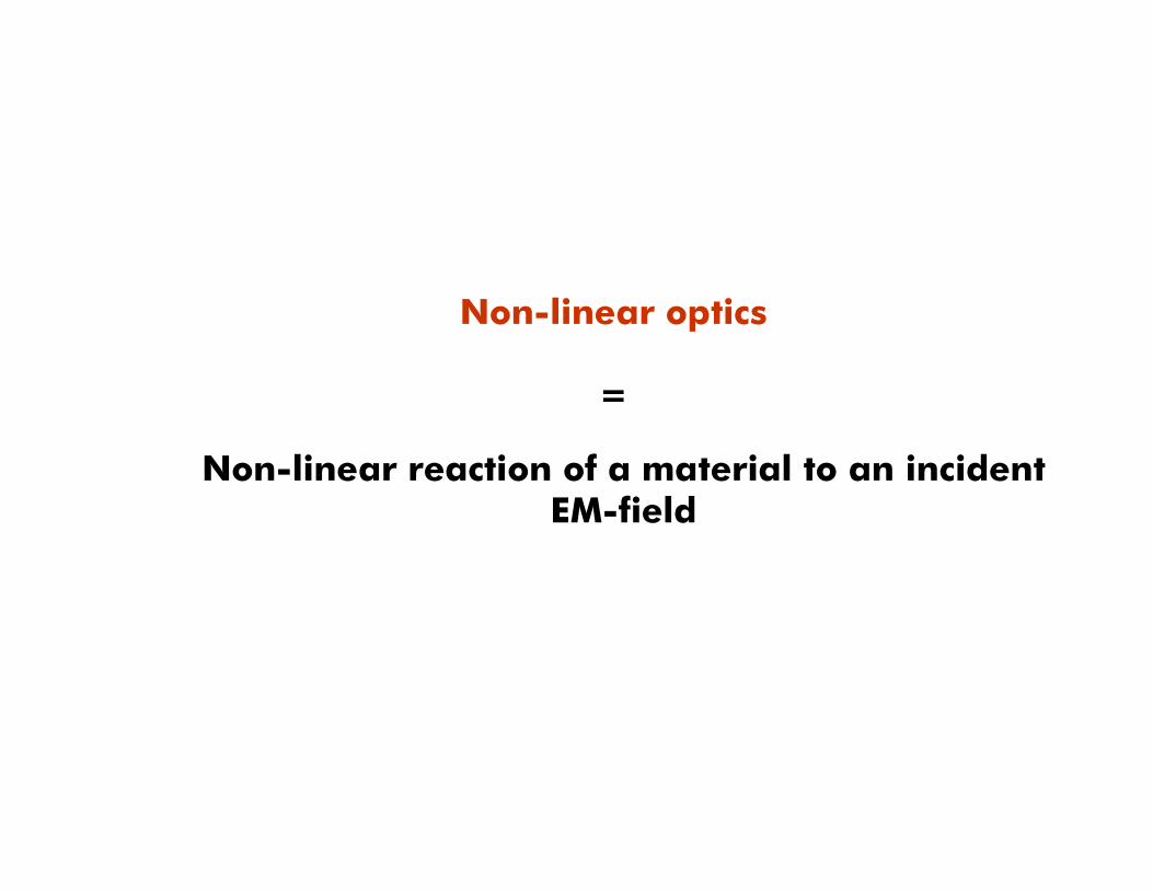
...)(~)(~)(~)(~ )3()2()1( +++= tPtPtPtP
)(~)(~ )1()1( tEtP χ=
)(~)(~ 2)2()2( tEtP χ=
)(~)(~ 3)3()3( tEtP χ=
(for a lossless, dispersionless medium with instanteneous reaction)
linear polarization
2nd order non-linear polarization
3rd order non-linear polarization
Polarization
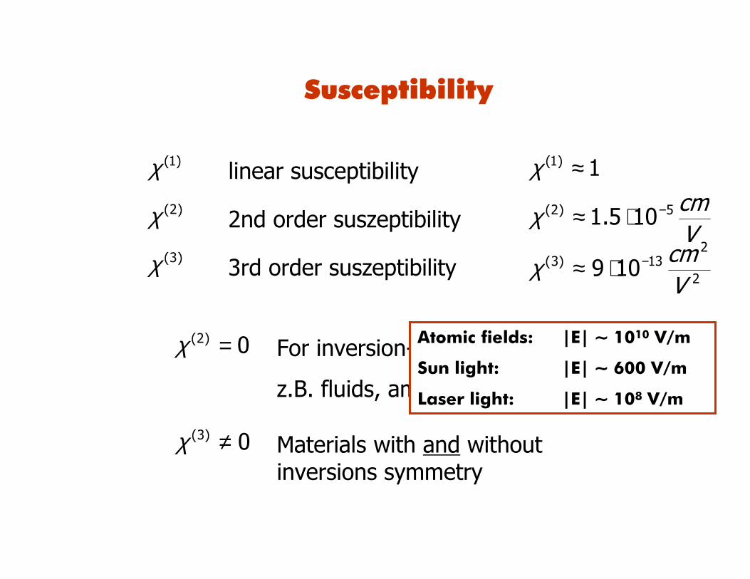
)1(χ)2(χ)3(χ
linear susceptibility
2nd order suszeptibility
3rd order suszeptibility
0)2( =χ For inversion-symmetric materials
z.B. fluids, amorphous materials
0)3( ≠χ Materials with and without inversions symmetry
2
213)3( 109
Vcm−⋅≈χ
Vcm5)2( 105.1 −⋅≈χ
1)1( ≈χ
Susceptibility
Atomic fields: |E| ~ 1010 V/m
Sun light: |E| ~ 600 V/m
Laser light: |E| ~ 108 V/m
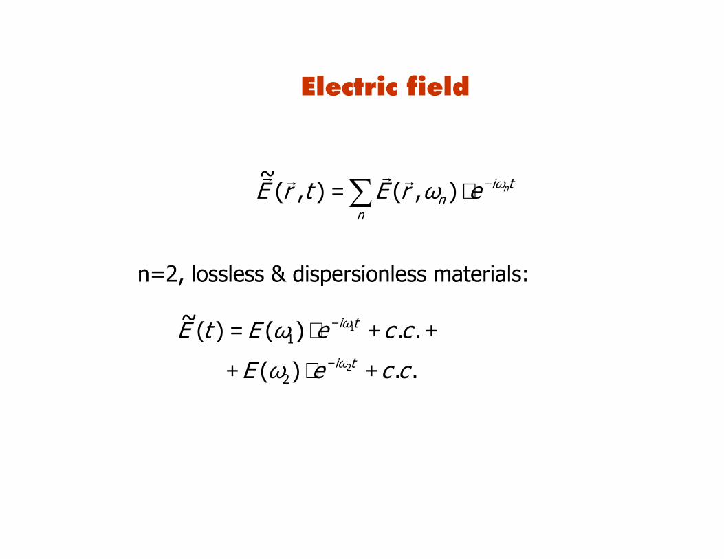
ti
nn
nerEtrE ωω −⋅=∑ ),(),(~ rrrr
n=2, lossless & dispersionless materials:
++⋅= − ..)()(~1
1 cceEtE tiωω
..)( 22 cceE ti +⋅+ − ωω
Electric field
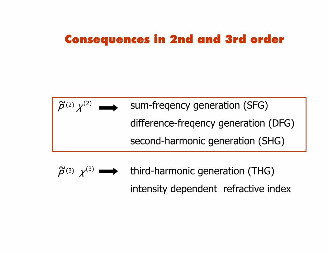
)2(~P
)3(χ
)2(χ
)3(~P
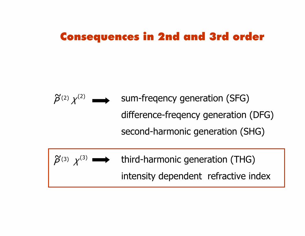
sum-freqency generation (SFG)
difference-freqency generation (DFG)
second-harmonic generation (SHG)
third-harmonic generation (THG)
intensity dependent refractive index
Consequences in 2nd and 3rd order
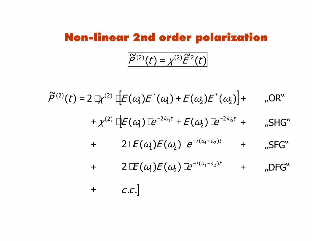
)(~)(~ 2)2()2( tEtP χ=
[ ] ++⋅⋅= )()()()(2)(~2
*21
*1
)2()2( ωωωωχ EEEEtP
[ titi eEeE 21 22
21
)2( )()( ωω ωωχ −− ⋅+⋅⋅+
tieEE )(21
21)()(2 ωωωω +−⋅⋅+ +
tieEE )(21
21)()(2 ωωωω −−⋅⋅ ++
+
]..cc+
„OR“
„SHG“
„SFG“
„DFG“
Non-linear 2nd order polarization
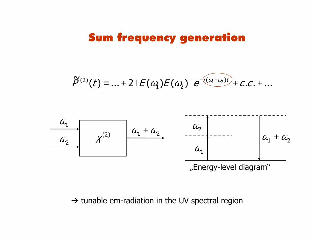
.....)()(2...)(~ )(21
)2( 21 ++⋅⋅+= +− cceEEtP ti ωωωω
)2(χ 21 ωω +1ω
2ω 21 ωω +1ω
2ω
tunable em-radiation in the UV spectral region
„Energy-level diagram“
Sum frequency generation
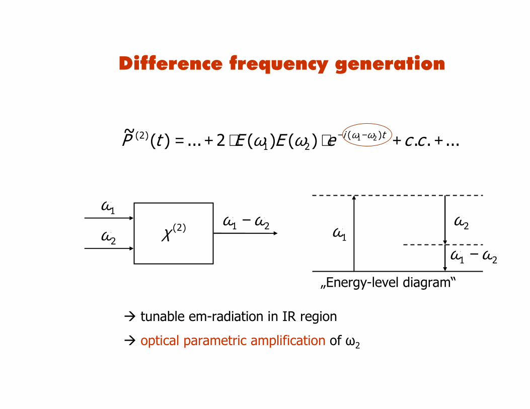
.....)()(2...)(~ )(21
)2( 21 ++⋅⋅+= −− cceEEtP ti ωωωω
)2(χ 21 ωω −1ω
2ω21 ωω −
1ω 2ω
tunable em-radiation in IR region
optical parametric amplification of ω2
„Energy-level diagram“
Difference frequency generation
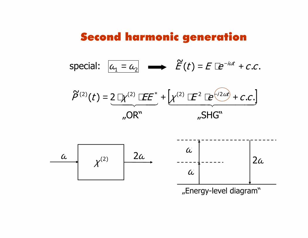
[ ]4444 34444 214434421 ..2)(~ 22)2(*)2()2( cceEEEtP ti +⋅⋅+⋅⋅= − ωχχ
)2(χω ω2 ω2ω
ω
..)(~ cceEtE ti +⋅= − ωspecial: 21 ωω =
„Energy-level diagram“
„OR“ „SHG“
Second harmonic generation
)2(~P
)3(χ
)2(χ
)3(~P
sum-freqency generation (SFG)
difference-freqency generation (DFG)
second-harmonic generation (SHG)
third-harmonic generation (THG)
intensity dependent refractive index
Consequences in 2nd and 3rd order
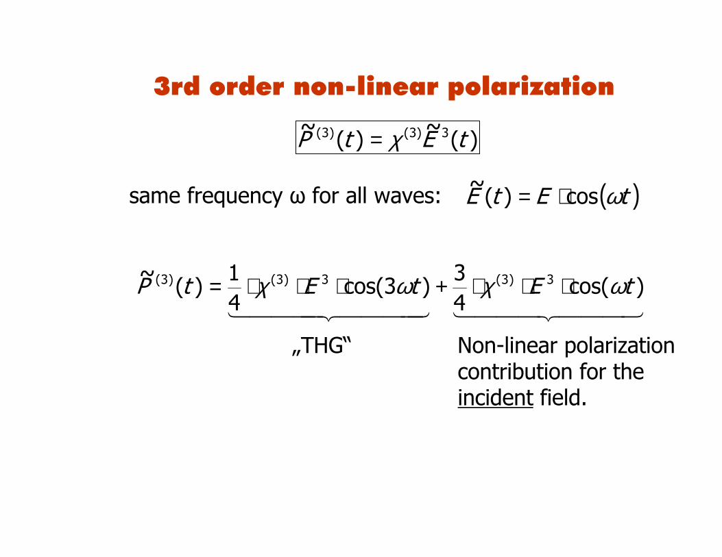
)(~)(~ 3)3()3( tEtP χ=
( )tEtE ωcos)(~ ⋅=same frequency ω for all waves:
444 3444 214444 34444 21)cos(
43)3cos(
41)(~ 3)3(3)3()3( tEtEtP ωχωχ ⋅⋅⋅+⋅⋅⋅=
„THG“ Non-linear polarization contribution for the incident field.
3rd order non-linear polarization
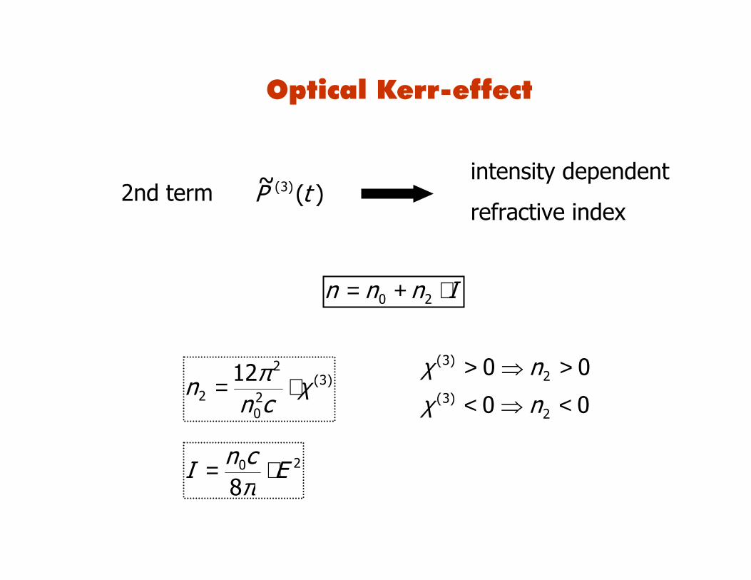
2nd term )(~ )3( tPintensity dependent
refractive index
Innn ⋅+= 20
20
8EcnI ⋅=
π
)3(20
2
212 χπ ⋅=
cnn
00
00
2)3(
2)3(
<⇒<
>⇒>
n
n
χχ
Optical Kerr-effect
0. Introduction
1. Reminder:E-Dynamics in homogenous media and at interfaces
2. Photonic Crystals2.1 Introduction2.2 1D Photonic Crystals2.3 2D and 3D Photonic Crystals2.4 Numerical Methods2.5 Fabrication2.6 Non-linear optics and Photonic Crystals
2.6.1 Non-linear optics2.6.2 Phase-matching2.6.3 Band-structure tuning2.6.4 All-optical switching
2.7 Quantumoptics2.8 Chiral Photonic Crystals2.9 Quasicrystals2.10 Photonic Crystal Fibers – „Holey“ Fibers
3. Metamaterials and Plasmonics3.1 Introduction3.2 Background3.2 Fabrication3.3 Experiments
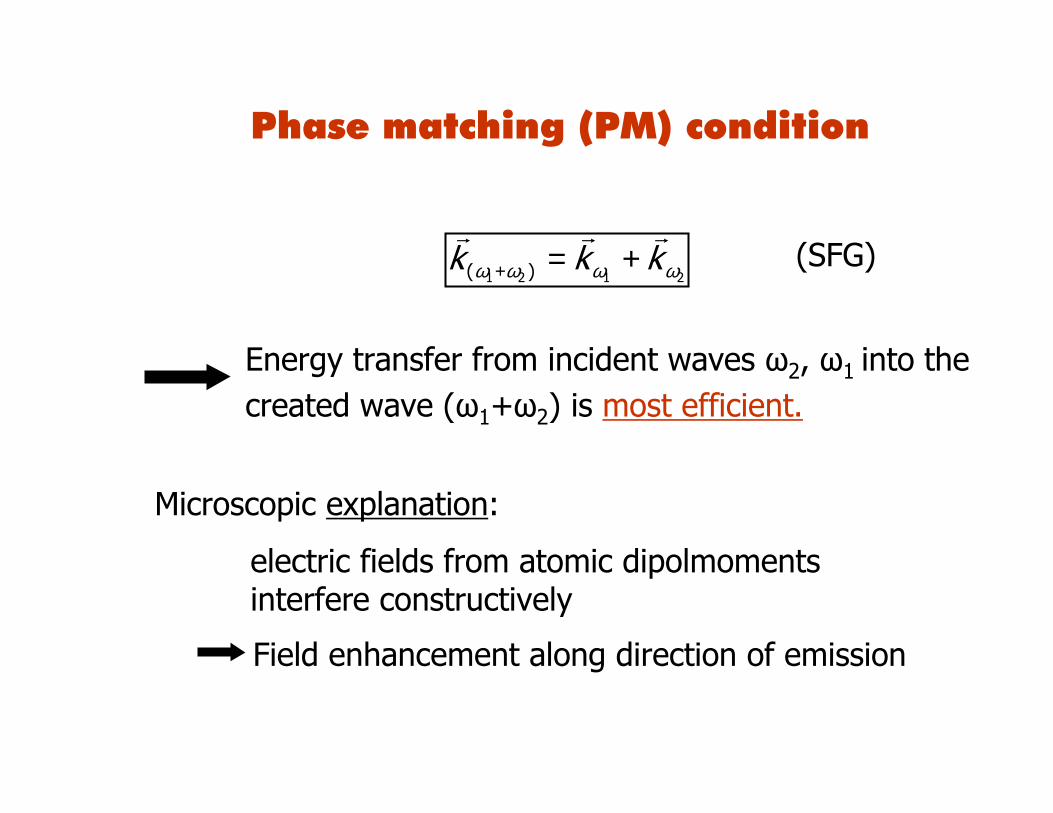
2121 )( ωωωω kkkrrr
+=+ (SFG)
Energy transfer from incident waves ω2, ω1 into the created wave (ω1+ω2) is most efficient.
Microscopic explanation:
electric fields from atomic dipolmoments interfere constructively
Field enhancement along direction of emission
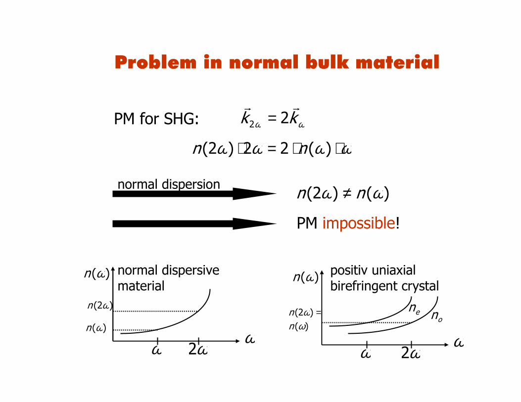
Phase matching (PM) condition
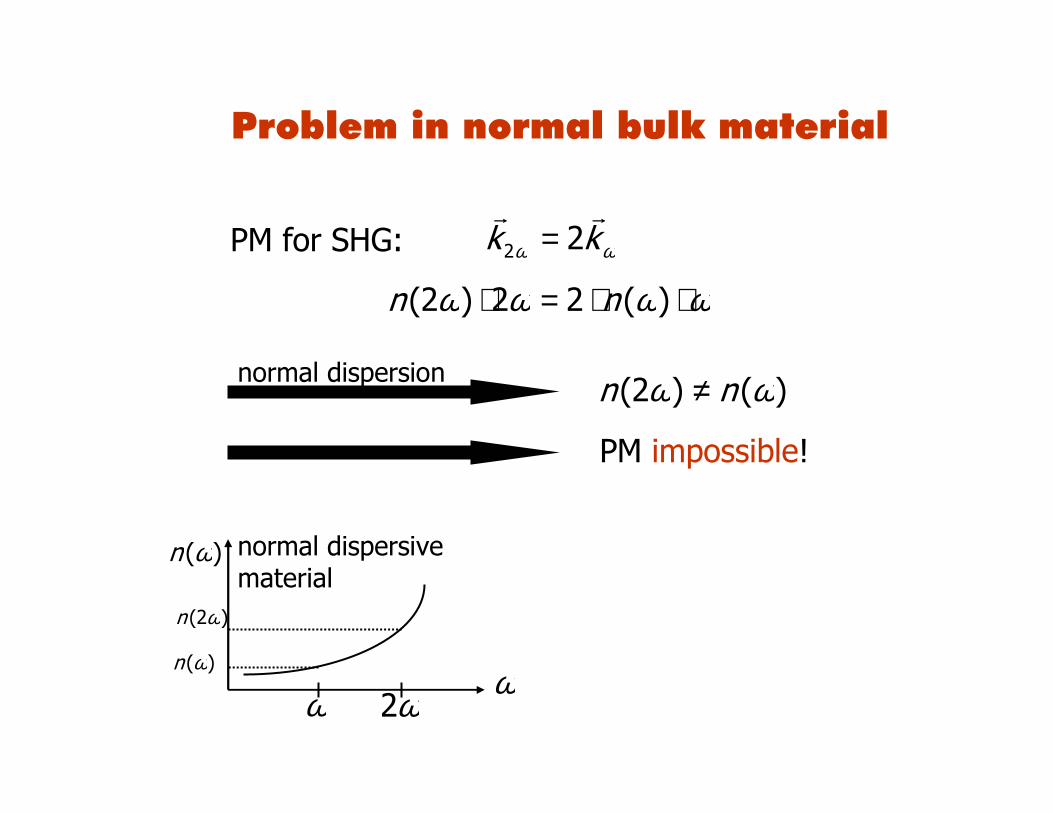
PM for SHG: ωω kkrr
22 =
ωωωω ⋅⋅=⋅ )(22)2( nn
normal dispersion )()2( ωω nn ≠
PM impossible!
ω
)(ωn
ω ω2
)2( ωn
)(ωn
normal dispersive material
Problem in normal bulk material
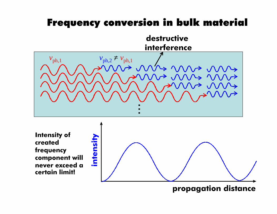
inte
nsi
ty
vph,1 vph,2 = vph,1
...
destructive interference
propagation distance
Intensity of created frequency component will never exceed a certain limit!
Frequency conversion in bulk material
PM for SHG: ωω kkrr
22 =
ωωωω ⋅⋅=⋅ )(22)2( nn
normal dispersion )()2( ωω nn ≠
PM impossible!
ω
)(ωn
ω ω2
)2( ωn
)(ωn
normal dispersive material
Problem in normal bulk material
ω
)(ωn
ω ω2
)()2(
ωω
nn =
onen
positiv uniaxial birefringent crystal
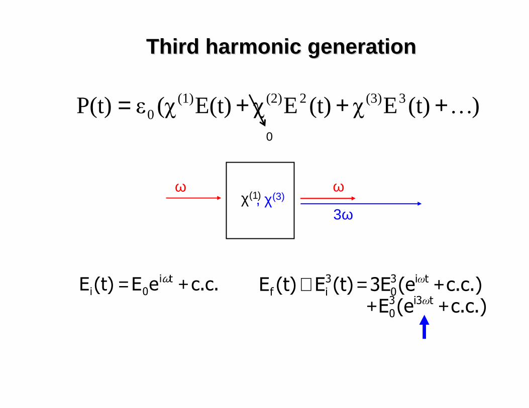
Third harmonic generationThird harmonic generation
)(t)Eχ(t)EχE(t)(χεP(t) 3(3)2(2)(1)0 K+++=
c.c.eE(t)E ti0i += ω
χ(1)ω ω
0
, χ(3)
3ω
c.c.)(eE c.c.)(e3E(t)E(t)E
ti330
ti30
3if
+++=∝
ω
ω
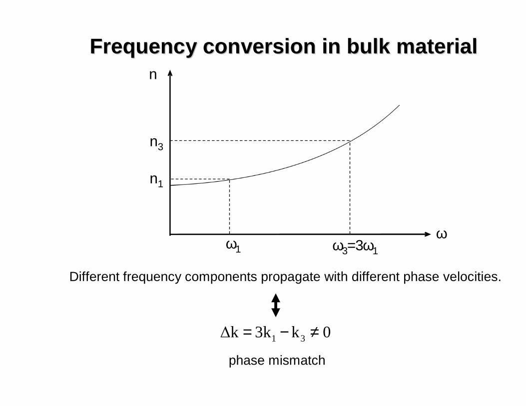
Frequency conversion in bulk materialFrequency conversion in bulk material
ω3=3ω1ω
ω1
n
n3
n1
Different frequency components propagate with different phase velocities.
0k3k∆k 31 ≠−=
phase mismatch
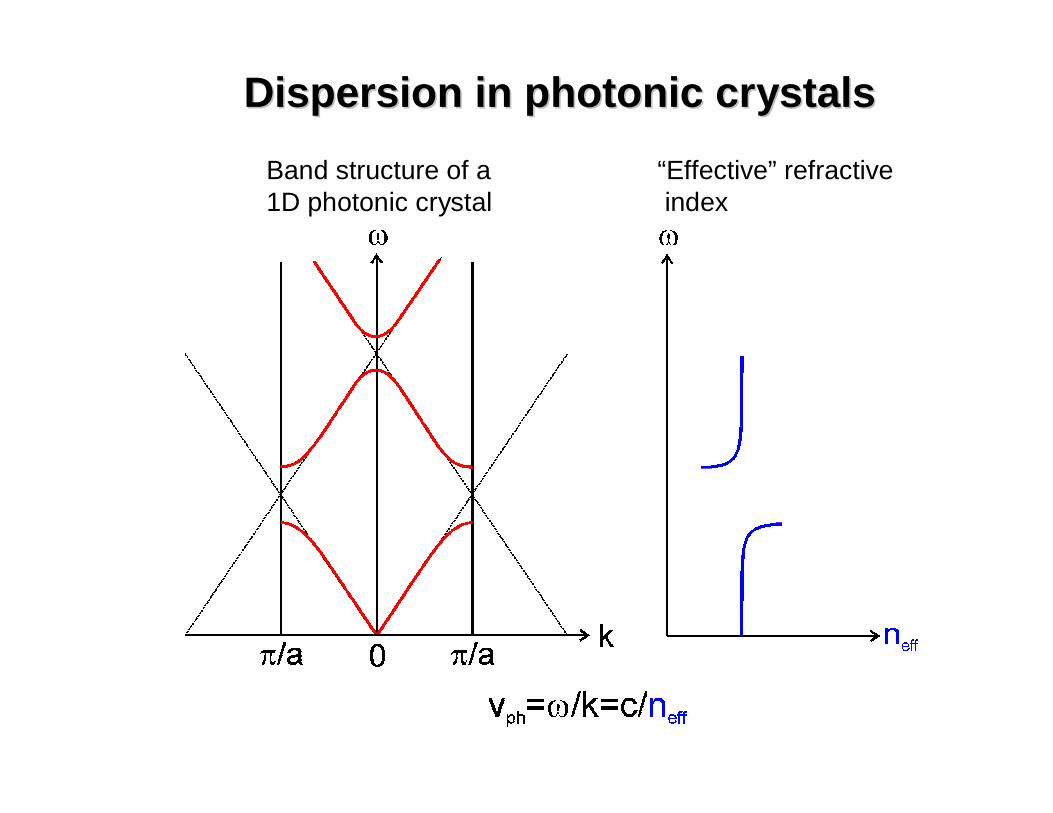
Dispersion in photonic crystalsDispersion in photonic crystals
Band structure of a 1D photonic crystal
“Effective” refractiveindex
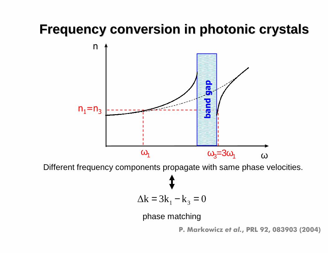
Frequency conversion in photonic crystalsFrequency conversion in photonic crystals
ω3=3ω1 ωω1
n
n1=n3
Different frequency components propagate with same phase velocities.
0k3k∆k 31 =−=
phase matching
P. Markowicz et al., PRL 92, 083903 (2004)
ban
d g
ap
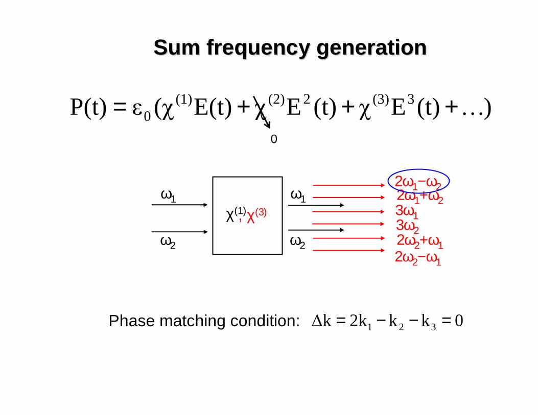
Sum frequency generationSum frequency generation
)(t)Eχ(t)EχE(t)(χεP(t) 3(3)2(2)(1)0 K+++=
ω2
χ(1)ω1 ω1
ω2
, χ(3)
2ω1+ω2
2ω2+ω1
2ω1−ω2
2ω2−ω1
3ω13ω2
0
Phase matching condition: 0kk2k∆k 321 =−−=
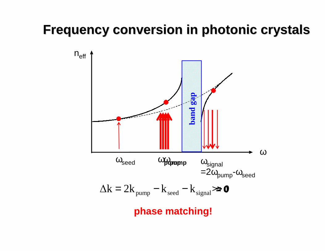
Frequency conversion in photonic crystalsFrequency conversion in photonic crystals
ωωseed
neff
phase matching!
band
gap
ωpump ωsignal=2ωpump-ωseed
>> 0signalseedpump kk2k∆k −−= > 0= 0< 0
ωpump
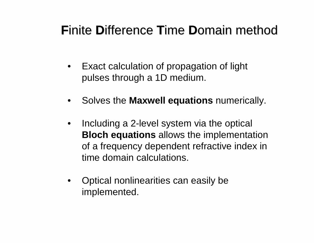
FFinite inite DDifference ifference TTime ime DDomain methodomain method
• Exact calculation of propagation of light pulses through a 1D medium.
• Solves the Maxwell equations numerically.
• Including a 2-level system via the optical Bloch equations allows the implementation of a frequency dependent refractive index in time domain calculations.
• Optical nonlinearities can easily be implemented.
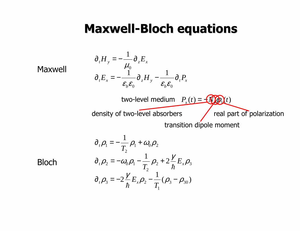
MaxwellMaxwell--Bloch equationsBloch equations
xtb
yzb
xt
xzyt
PHE
EH
∂−∂−=∂
∂−=∂
00
011
1
εεεε
µ
)(1
2
21
1
3031
23
322
102
2012
1
ρρργρ
ργρρωρ
ρωρρ
−−−=∂
+−−=∂
+−=∂
TE
ET
T
xt
xt
t
h
h
Maxwell
Bloch
transition dipole moment
)()( 1 tNtPx γρ−=two-level medium
density of two-level absorbers real part of polarization
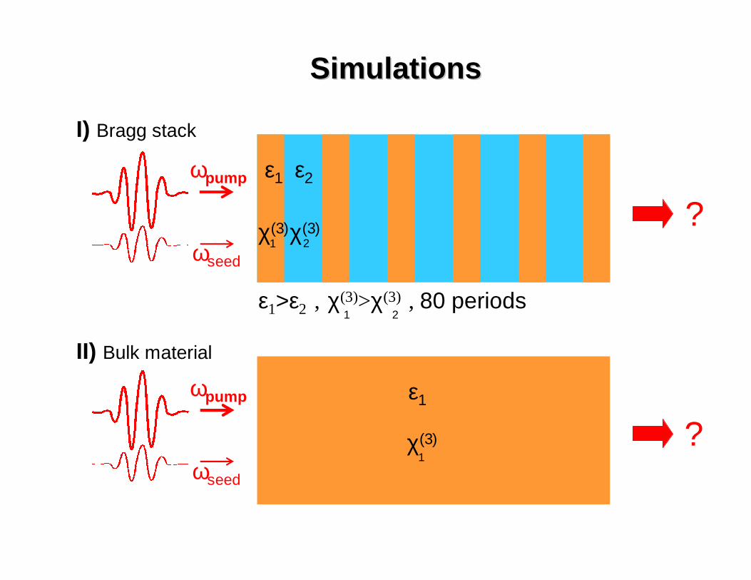
SimulationsSimulations
ε1 ε2
II) Bulk material
I) Bragg stack
ε1
?
?
ωpump
ωseed
ε1>ε2 , χ(3)>χ(3) , 80 periods
ωpump
ωseed
χ(3)1
χ(3)2
1 2
χ(3)1
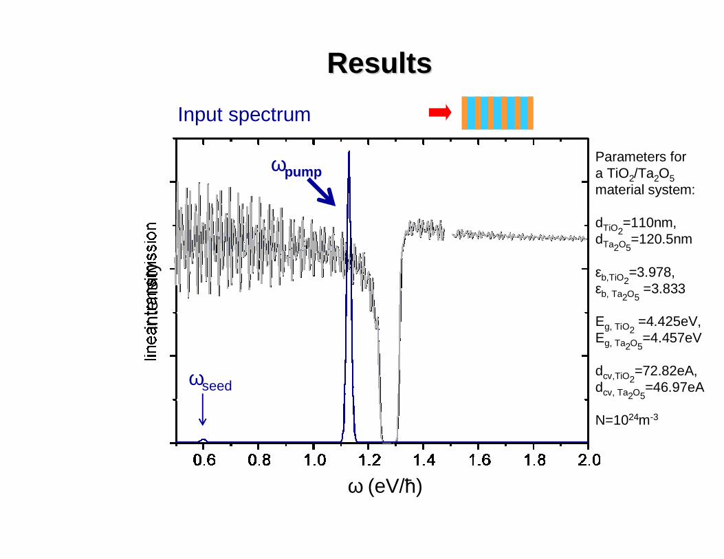
ResultsResults
ωseed
ωpump
Input spectrum
ω (eV/ħ)
inte
nsity
Parameters fora TiO2/Ta2O5material system:
dTiO2=110nm,
dTa2O5=120.5nm
εb,TiO2=3.978,
εb, Ta2O5=3.833
Eg, TiO2=4.425eV,
Eg, Ta2O5=4.457eV
dcv,TiO2=72.82eA,
dcv, Ta2O5=46.97eA
N=1024m-3
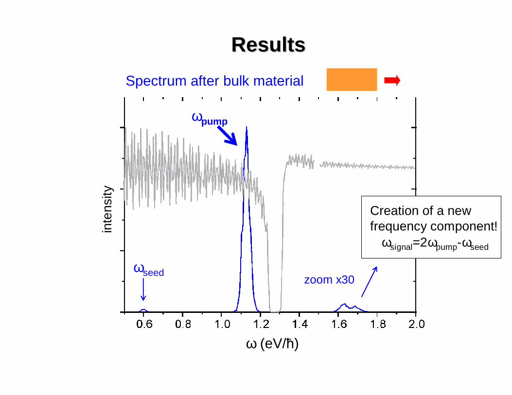
ResultsResults
ωseed
ωpump
Spectrum after bulk material
ω (eV/ħ)
inte
nsity
zoom x30
ωsignal=2ωpump-ωseed
Creation of a newfrequency component!
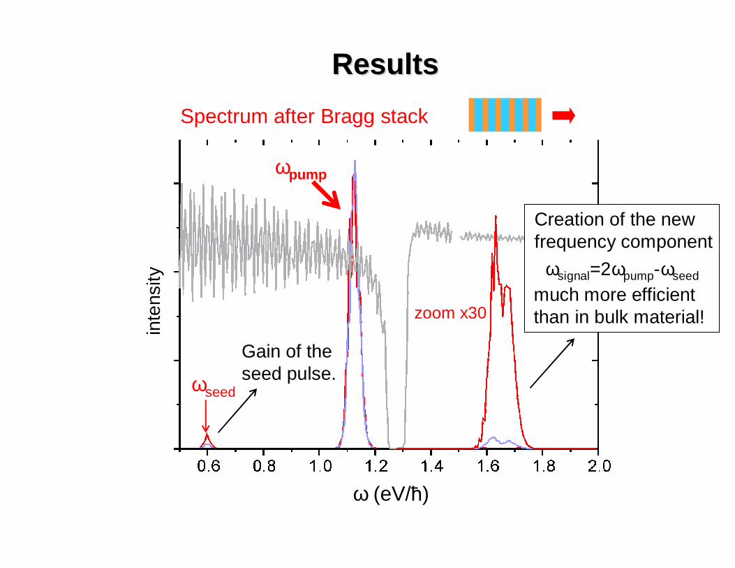
ResultsResults
Spectrum after Bragg stack
ωseed
ωpump
Gain of theseed pulse.
ω (eV/ħ)
inte
nsity ωsignal=2ωpump-ωseed
Creation of the newfrequency component
much more efficient than in bulk material!zoom x30
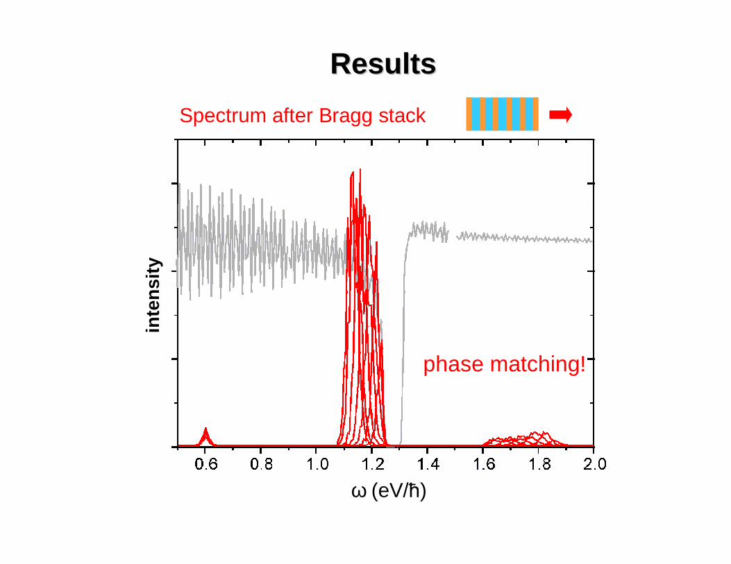
ResultsResults
Spectrum after Bragg stack
phase matching!
ω (eV/ħ)
inte
nsi
ty
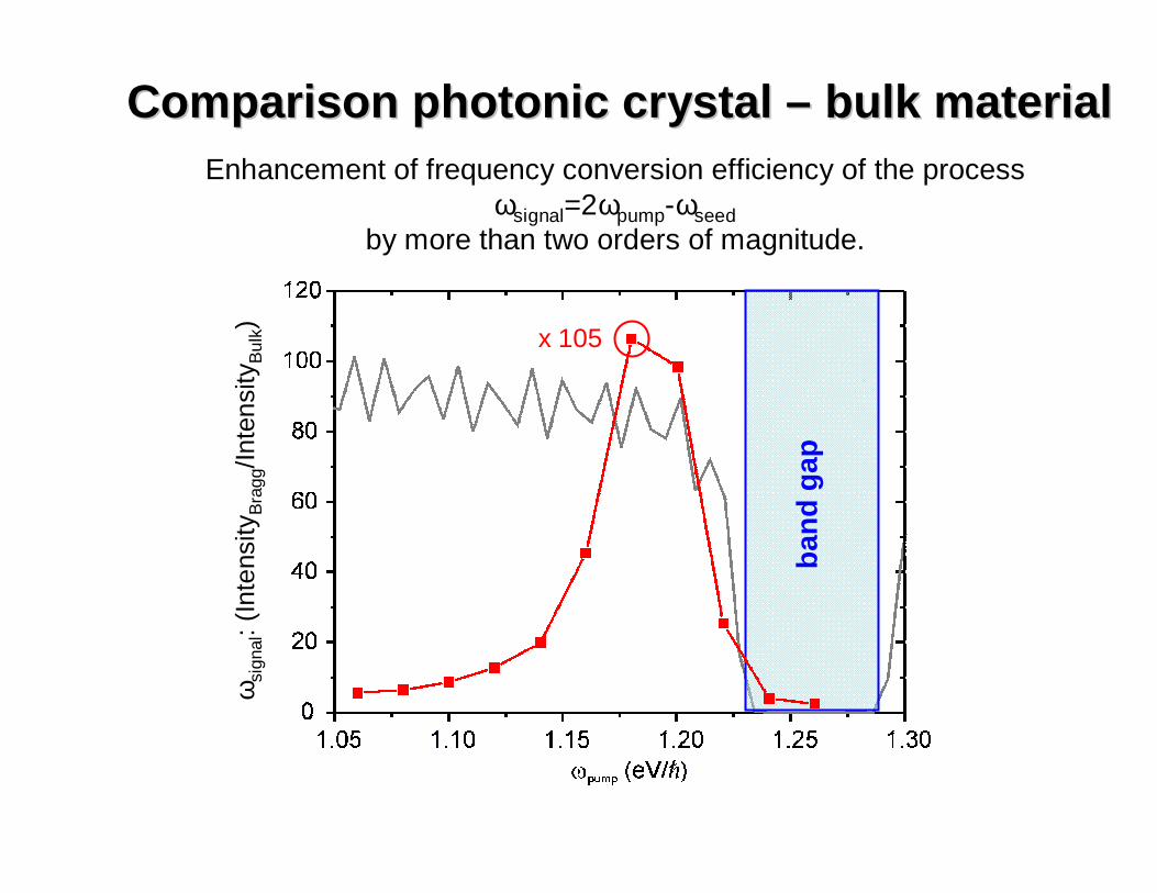
Comparison photonic crystal Comparison photonic crystal –– bulk materialbulk material
ban
d g
ap
Enhancement of frequency conversion efficiency of the processωsignal=2ωpump-ωseed
by more than two orders of magnitude.ω
sign
al: (
Inte
nsity
Bra
gg/In
tens
ityB
ulk) x 105
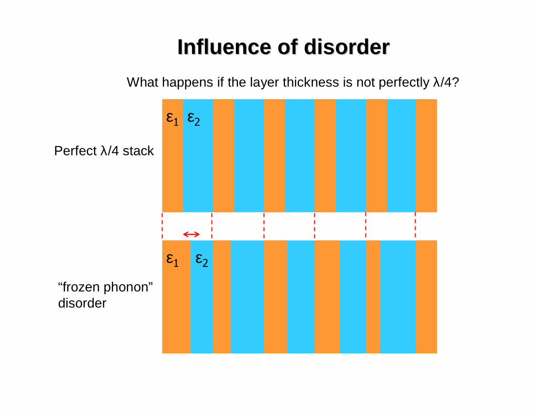
Influence of disorderInfluence of disorder
ε1 ε2
What happens if the layer thickness is not perfectly λ/4?
Perfect λ/4 stack
“frozen phonon”disorder
ε1 ε2
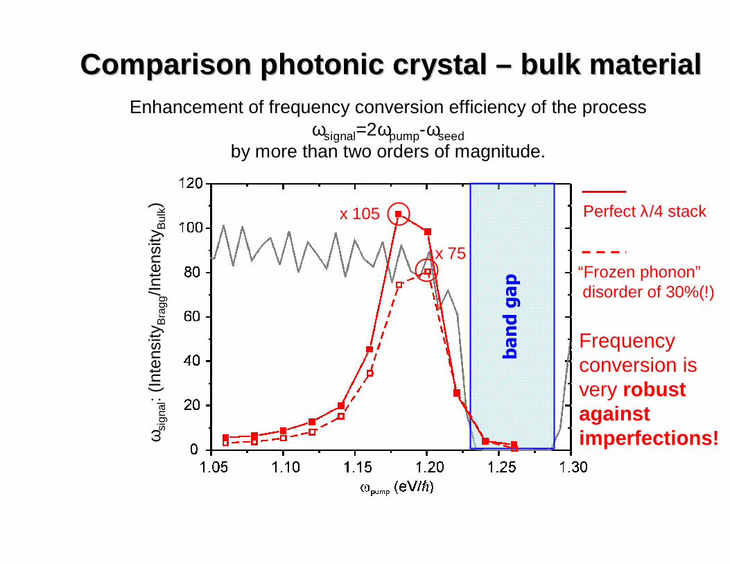
Comparison photonic crystal Comparison photonic crystal –– bulk materialbulk material
ban
d g
ap
Enhancement of frequency conversion efficiency of the processωsignal=2ωpump-ωseed
by more than two orders of magnitude.ω
sign
al: (
Inte
nsity
Bra
gg/In
tens
ityB
ulk) x 105
x 75
Frequencyconversion isvery robustagainstimperfections!
“Frozen phonon”disorder of 30%(!)
Perfect λ/4 stack
inte
nsity
inte
nsity
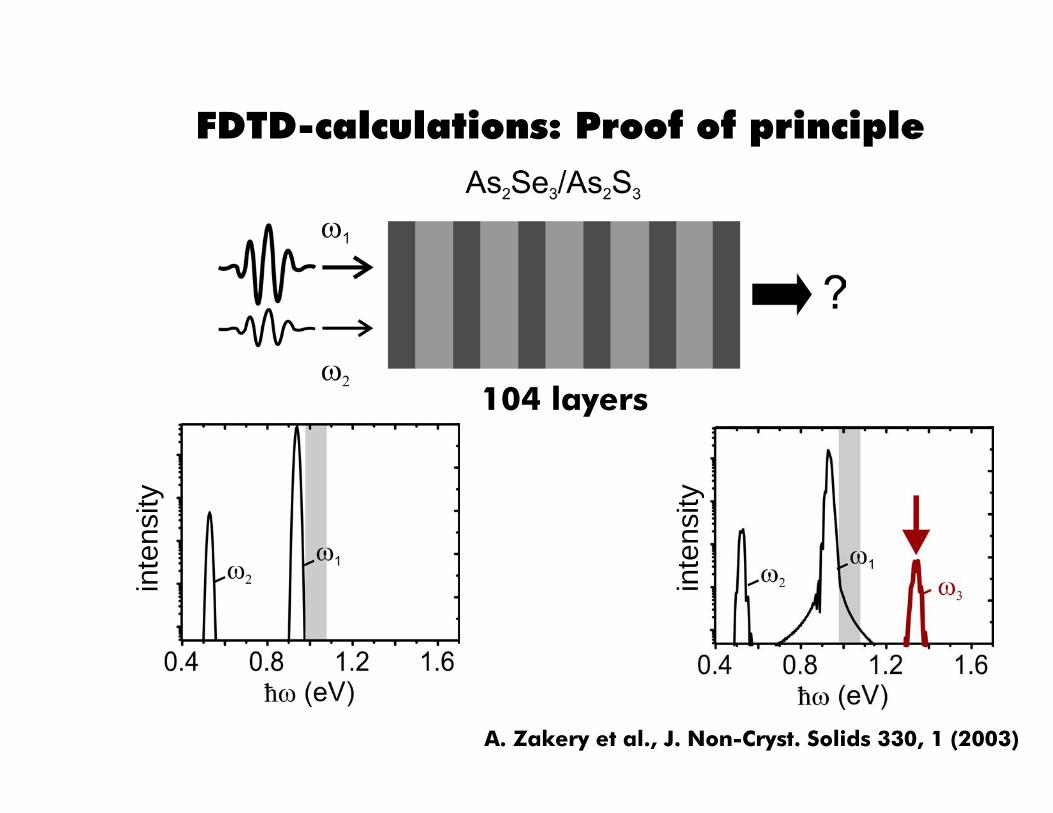
FDTD-calculations: Proof of principle
A. Zakery et al., J. Non-Cryst. Solids 330, 1 (2003)
104 layers
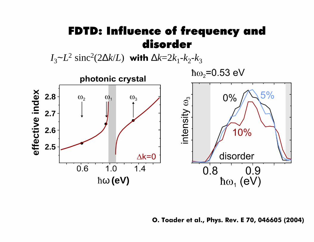
FDTD: Influence of frequency and disorder
2.5
2.6
2.7
2.8
effe
ctiv
e in
dex
O. Toader et al., Phys. Rev. E 70, 046605 (2004)
I3~L2 sinc2(2∆k/L) with ∆k=2k1-k2-k3
ћω (eV)
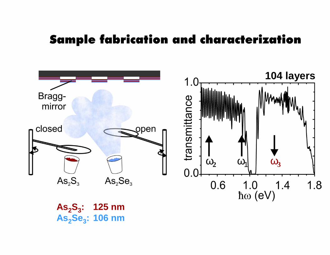
Sample fabrication and characterization
ω2 ω1 ω3
As2S3: 125 nmAs2Se3: 106 nm
104 layers
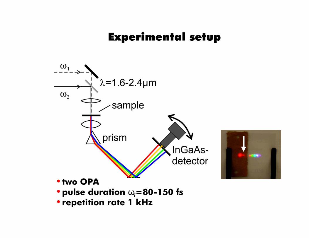
Experimental setup
•two OPA •pulse duration ωi=80-150 fs•repetition rate 1 kHz
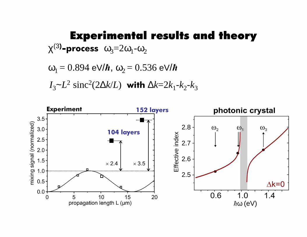
Theory
Experimental results and theoryχ(3)-process ω3=2ω1-ω2
I3~L2 sinc2(2∆k/L) with ∆k=2k1-k2-k3
Experiment
2.5
2.6
2.7
2.8
Effe
ctiv
e in
dex
ω1 = 0.894 eV/ћ, ω2 = 0.536 eV/ћ
ћω (eV)
104 layers
152 layers
0. Introduction
1. Reminder:E-Dynamics in homogenous media and at interfaces
2. Photonic Crystals2.1 Introduction2.2 1D Photonic Crystals2.3 2D and 3D Photonic Crystals2.4 Numerical Methods2.5 Fabrication2.6 Non-linear optics and Photonic Crystals
2.6.1 Non-linear optics2.6.2 Phase-matching2.6.3 Band-structure tuning2.6.4 All-optical switching
2.7 Quantumoptics2.8 Chiral Photonic Crystals2.9 Quasicrystals2.10 Photonic Crystal Fibers – „Holey“ Fibers
3. Metamaterials and Plasmonics3.1 Introduction3.2 Background3.2 Fabrication3.3 Experiments
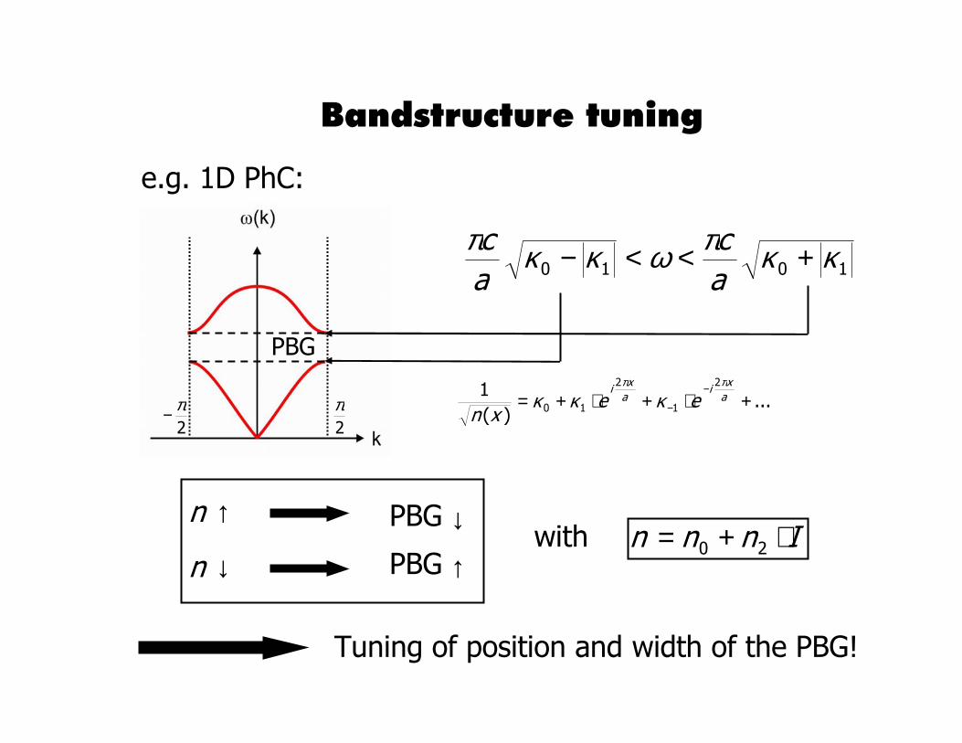
Tuning of position and width of the PBG!
...)(
1 2
1
2
10 +⋅+⋅+=−
−axi
axi
eexn
ππ
κκκ
e.g. 1D PhC:
PBG
2π
2π−
1010 κκπωκκπ +<<−ac
ac
↑n ↓
↑↓n
PBG
PBGwith Innn ⋅+= 20
Bandstructure tuning
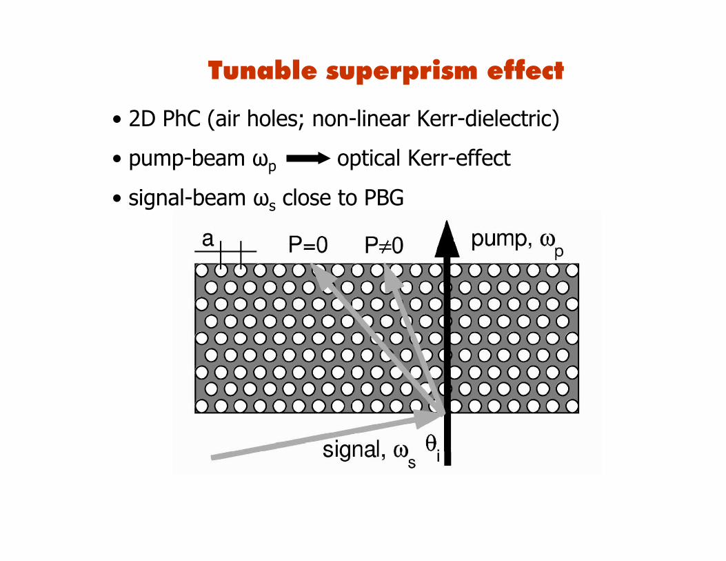
• 2D PhC (air holes; non-linear Kerr-dielectric)
• pump-beam ωp optical Kerr-effect
• signal-beam ωs close to PBG
Tunable superprism effect
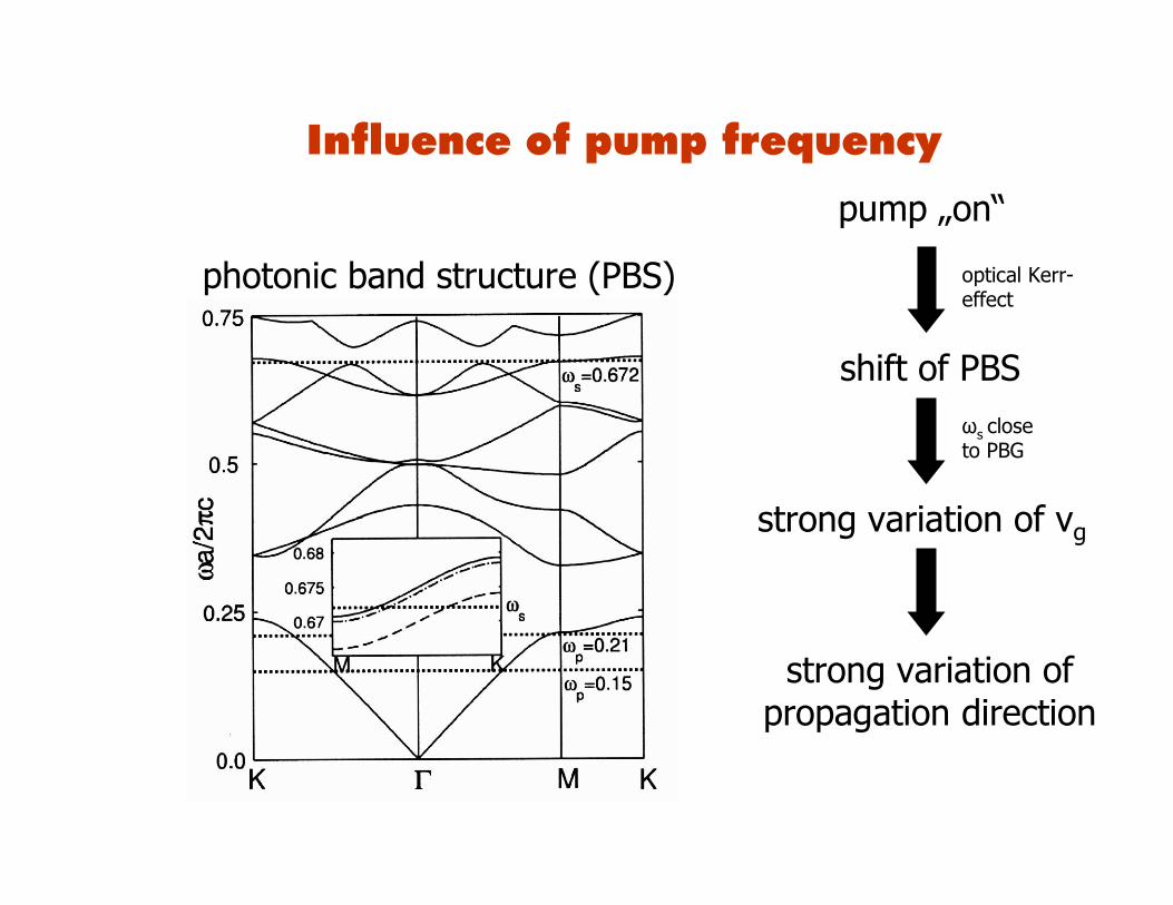
pump „on“
shift of PBS
optical Kerr-effect
strong variation of vg
ωs close to PBG
strong variation of propagation direction
photonic band structure (PBS)
Influence of pump frequency
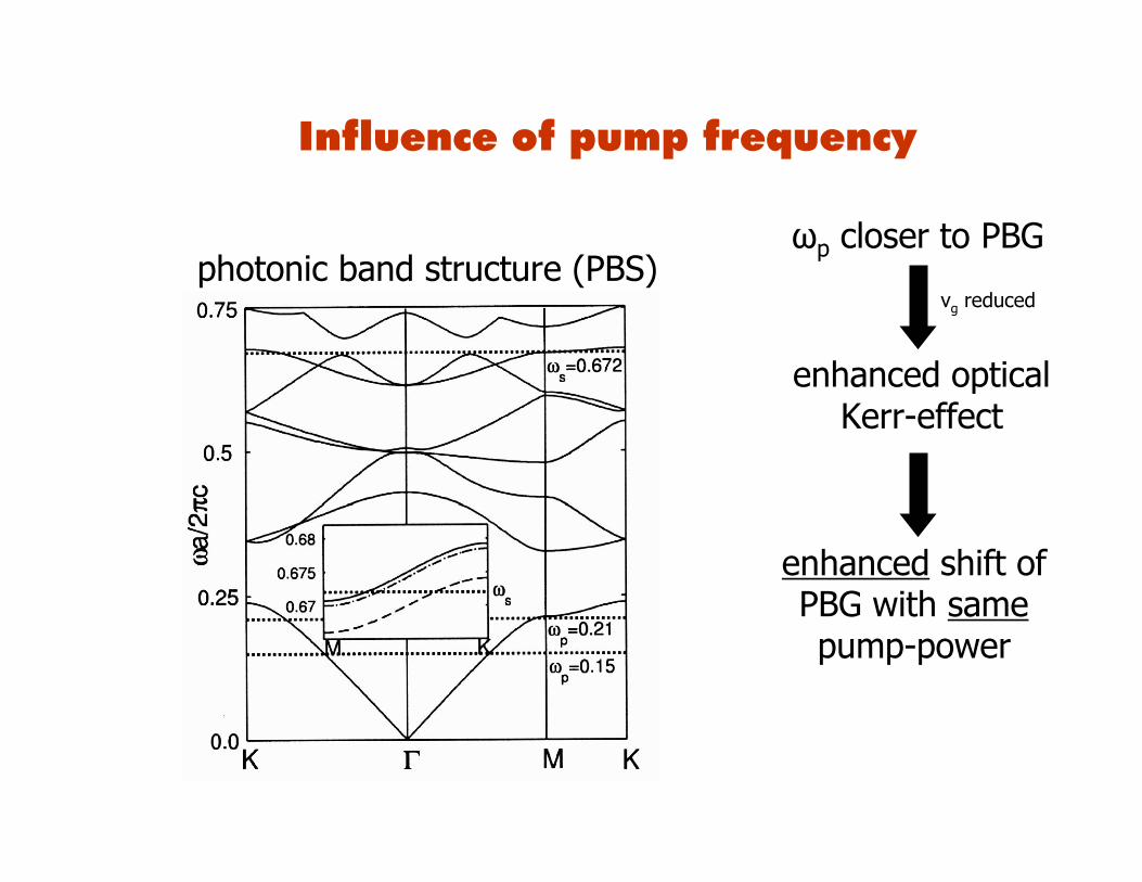
ωp closer to PBG
vg reduced
enhanced optical Kerr-effect
enhanced shift of PBG with samepump-power
Influence of pump frequency
photonic band structure (PBS)
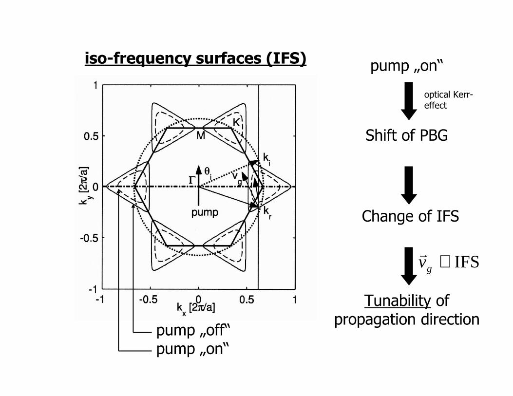
iso-frequency surfaces (IFS)
pump „off“ pump „on“
pump „on“
Shift of PBG
optical Kerr-effect
Tunability of propagation direction
Change of IFS
IFS⊥gvr
0. Introduction
1. Reminder:E-Dynamics in homogenous media and at interfaces
2. Photonic Crystals2.1 Introduction2.2 1D Photonic Crystals2.3 2D and 3D Photonic Crystals2.4 Numerical Methods2.5 Fabrication2.6 Non-linear optics and Photonic Crystals
2.6.1 Non-linear optics2.6.2 Phase-matching2.6.3 Band-structure tuning2.6.4 All-optical switching
2.7 Quantumoptics2.8 Chiral Photonic Crystals2.9 Quasicrystals2.10 Photonic Crystal Fibers – „Holey“ Fibers
3. Metamaterials and Plasmonics3.1 Introduction3.2 Background3.2 Fabrication3.3 Experiments
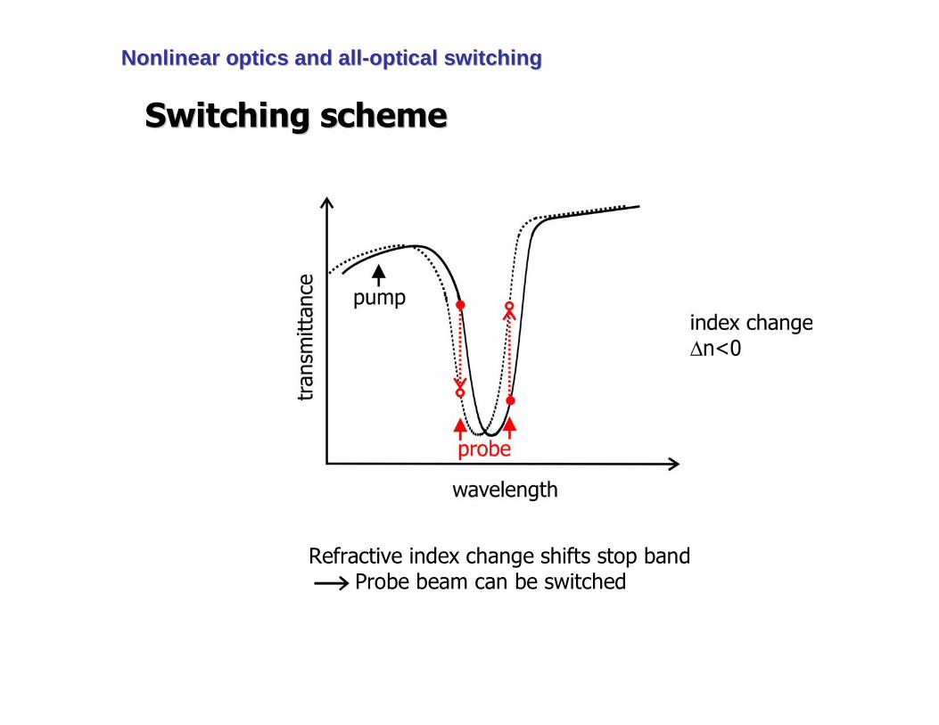
Switching schemeSwitching scheme
Refractive index change shifts stop bandProbe beam can be switched
Nonlinear optics and allNonlinear optics and all--optical switchingoptical switching
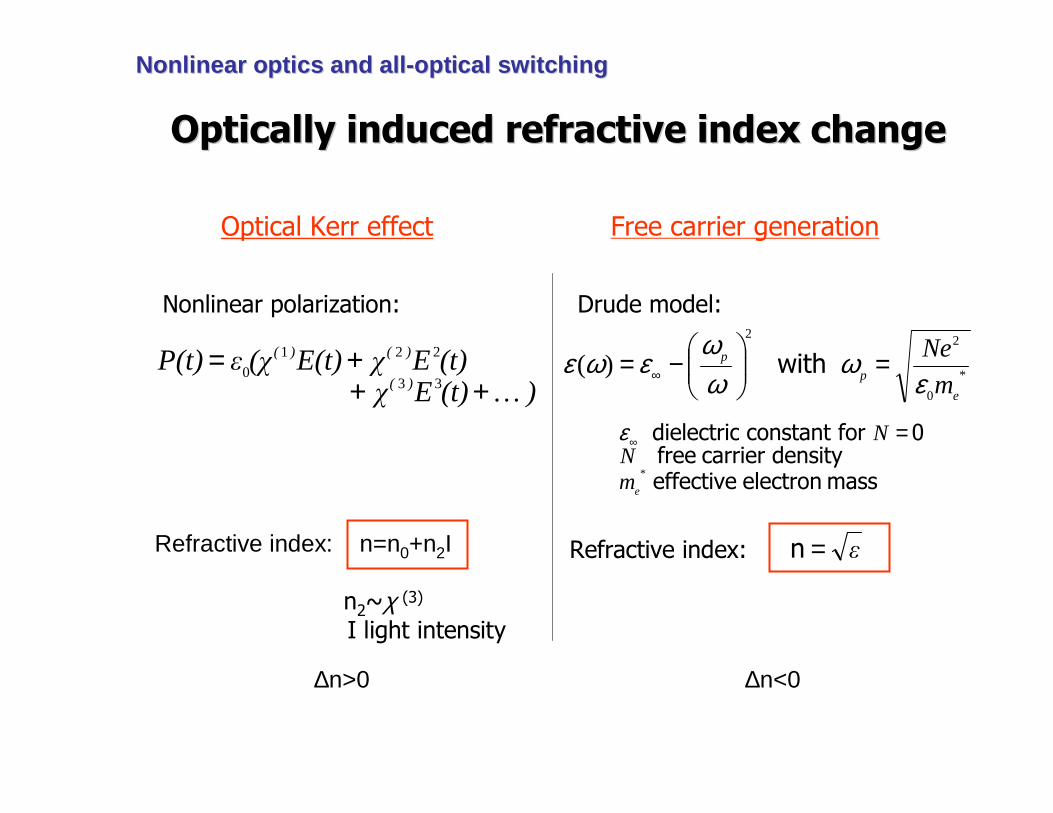
Optically induced refractive index changeOptically induced refractive index change
Optical Kerr effect Free carrier generation
ε=n
∆n<0∆n>0
mass electron effective densitycarrier free
0for constant dielectric
*
emN
N =∞ε
Nonlinear polarization:
)(t)Eχ (t)EχE(t)(χεP(t)
)(
)()(
K+++=
33
221
0
Refractive index: n=n0+n2I
n2~χ (3)
I light intensity
*
0
22
)(e
p
p
m
Ne
εω
ωω
εωε =
−= ∞ with
Drude model:
Refractive index:
Nonlinear optics and allNonlinear optics and all--optical switchingoptical switching
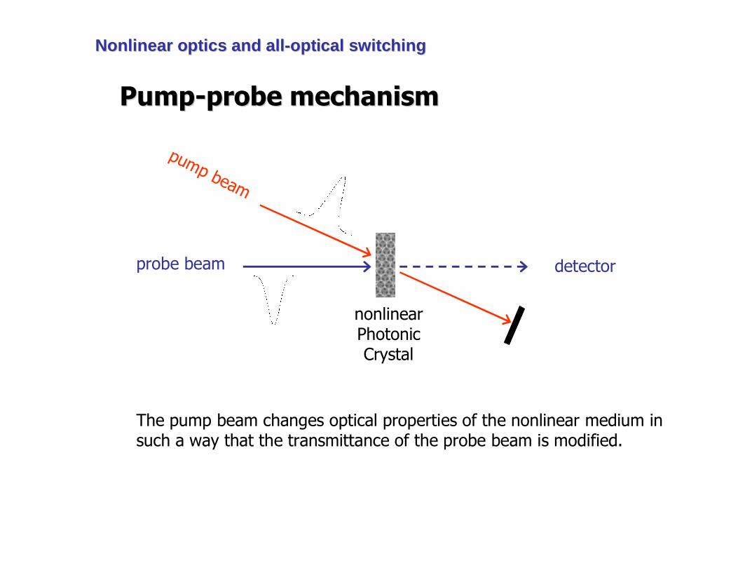
PumpPump--probe mechanismprobe mechanism
pump beam
probe beam
nonlinearPhotonicCrystal
detector
The pump beam changes optical properties of the nonlinear medium in such a way that the transmittance of the probe beam is modified.
Nonlinear optics and allNonlinear optics and all--optical switchingoptical switching
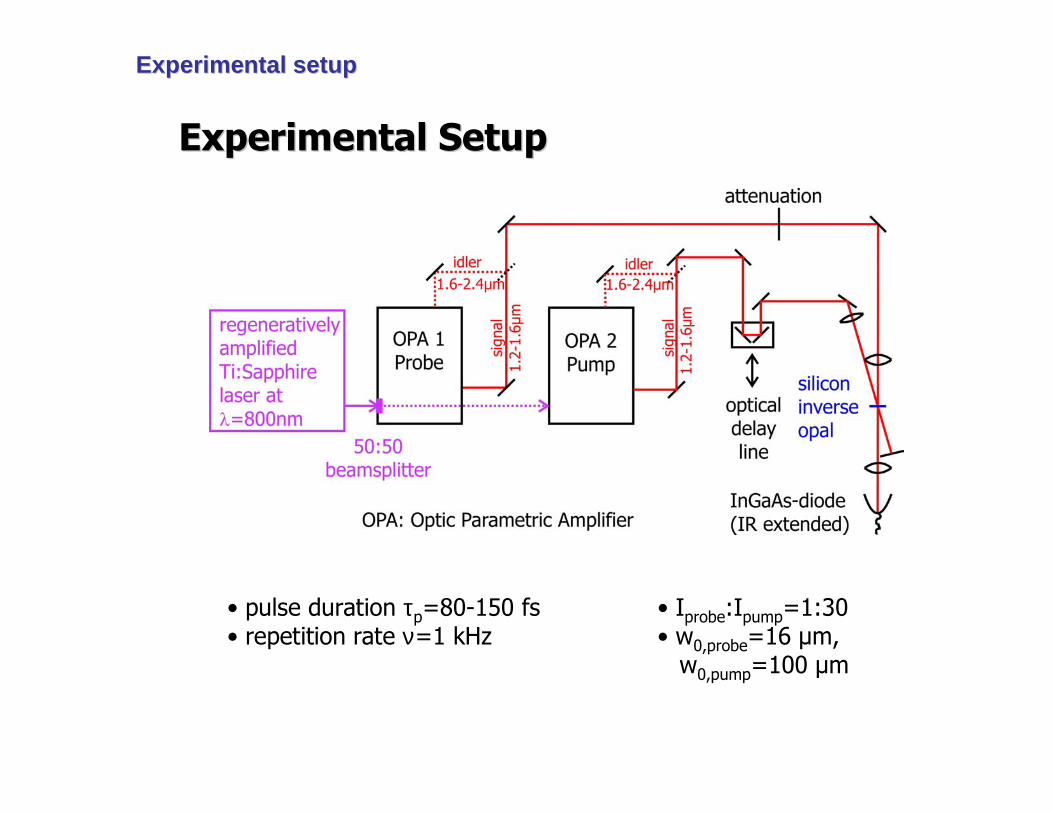
Experimental SetupExperimental Setup
• pulse duration τp=80-150 fs• repetition rate ν=1 kHz
• Iprobe:Ipump=1:30• w0,probe=16 µm,
w0,pump=100 µm
Experimental setupExperimental setup
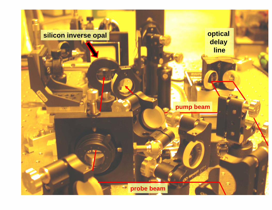
probe beam
pump beam
optical delay line
silicon inverse opal
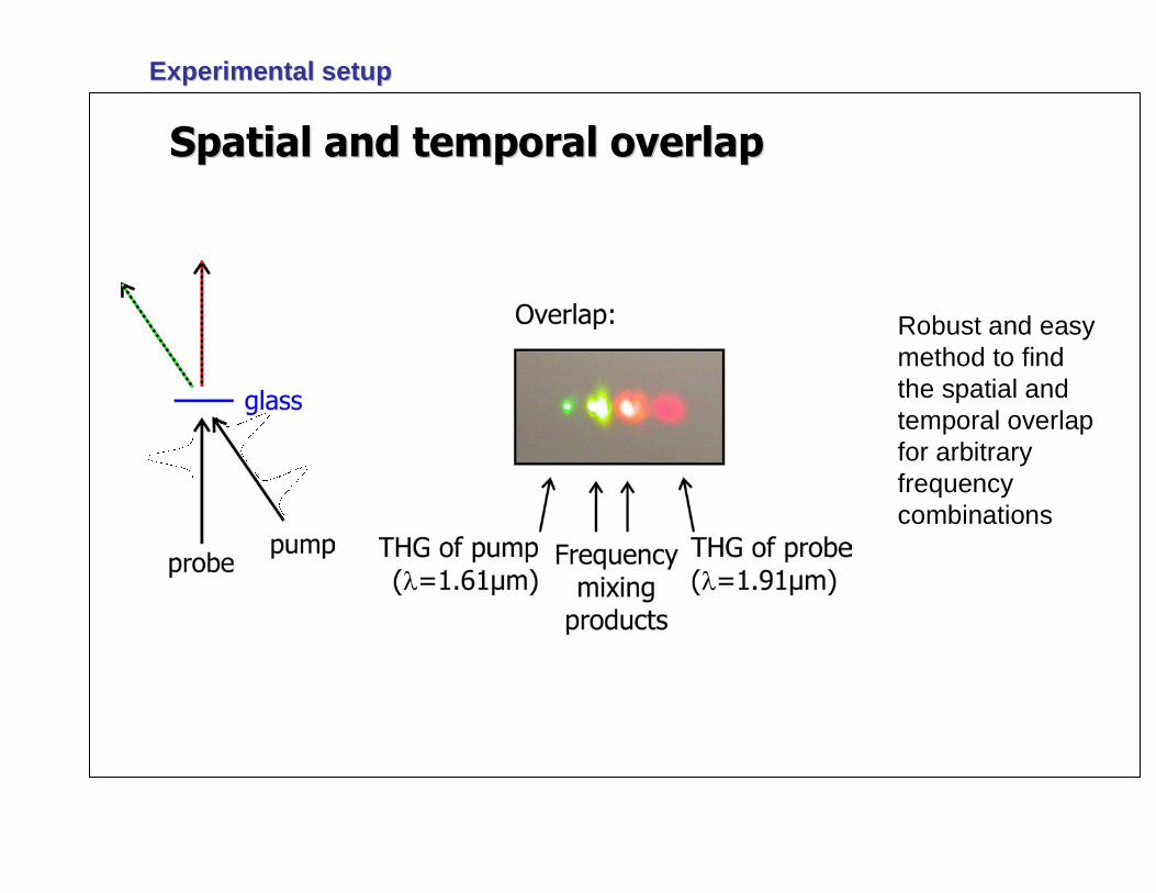
Spatial and temporal overlapSpatial and temporal overlap
Robust and easymethod to findthe spatial and temporal overlapfor arbitraryfrequency combinations
Experimental setupExperimental setup
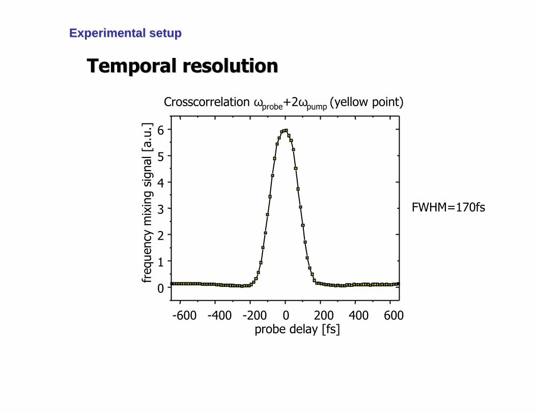
Temporal resolutionTemporal resolution
-600 -400 -200 0 200 400 600
0
1
2
3
4
5
6fr
eque
ncy
mix
ing
sign
al [
a.u.
]
probe delay [fs]
Crosscorrelation ωprobe+2ωpump (yellow point)
FWHM=170fs
Experimental setupExperimental setup
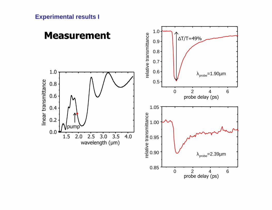
MeasurementMeasurement
Experimental results IExperimental results I
0.85
0.90
0.95
1.00
1.05
rela
tive
tran
smitt
ance
0 2 4 6probe delay (ps)
λprobe=2.39µm
0 2 4 6
0.5
0.6
0.7
0.8
0.9
1.0
rela
tive
tran
smitt
ance
probe delay (ps)
λprobe=1.90µm
∆T/T=49%
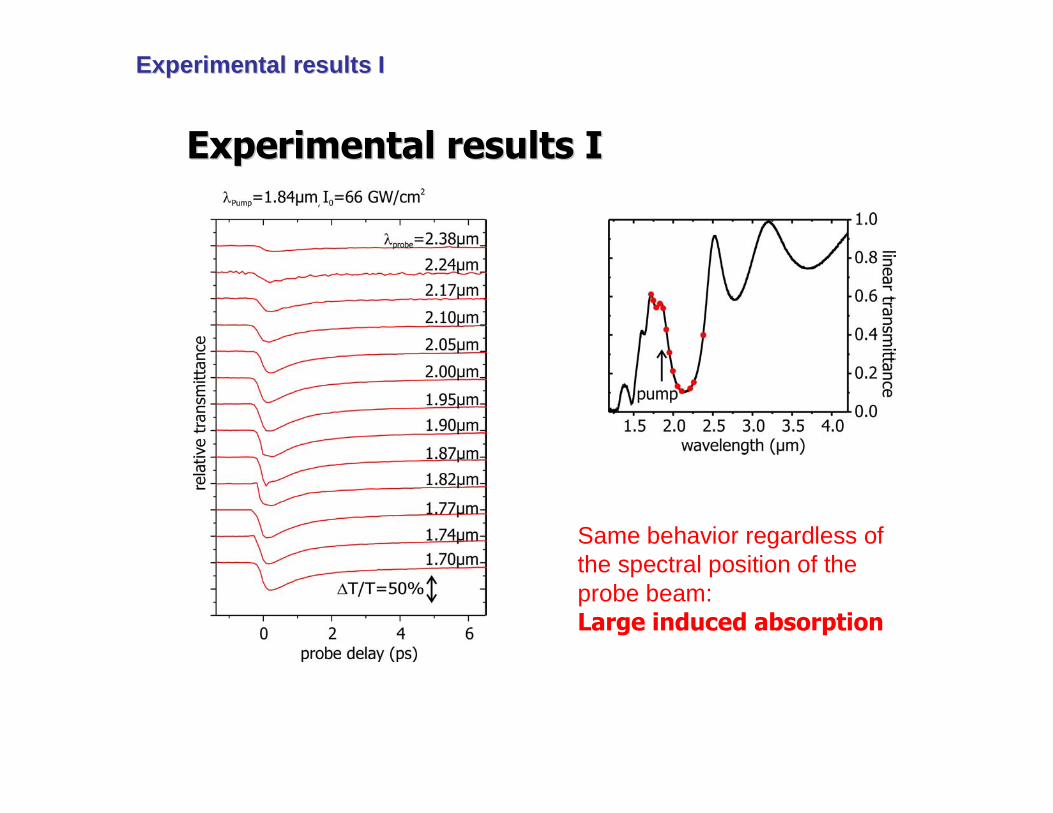
Experimental results IExperimental results I
Same behavior regardless of the spectral position of the probe beam:Large induced absorption
Experimental results IExperimental results I
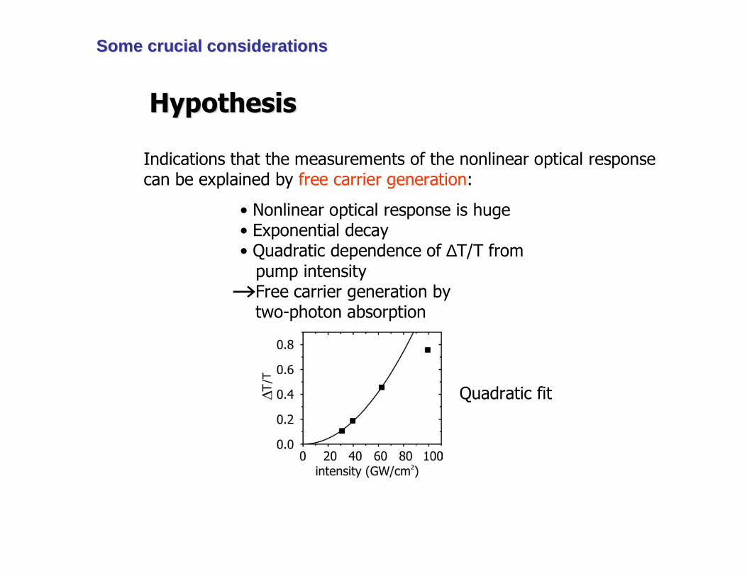
HypothesisHypothesis
Indications that the measurements of the nonlinear optical response can be explained by free carrier generation:
• Nonlinear optical response is huge• Exponential decay• Quadratic dependence of ∆T/T from
pump intensityFree carrier generation by two-photon absorption
Quadratic fit
Some crucial considerationsSome crucial considerations
/T
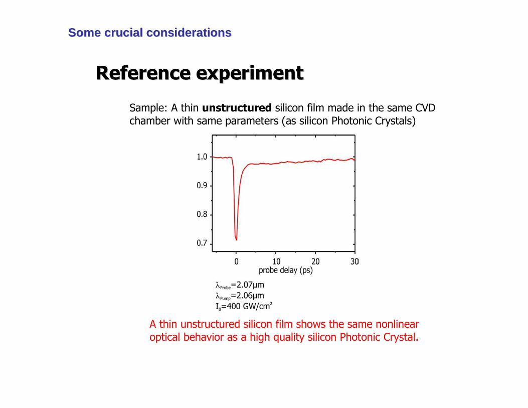
Reference experimentReference experiment
Sample: A thin unstructured silicon film made in the same CVD chamber with same parameters (as silicon Photonic Crystals)
A thin unstructured silicon film shows the same nonlinear optical behavior as a high quality silicon Photonic Crystal.
Some crucial considerationsSome crucial considerations
DrudeDrude modelmodel
( )
+
++
−= ∞ 2322*0
2
)/1(
)/1(
/1
1)(
τωωτ
τωεεωε i
m
Ne
e
τ =0.5fs for hydrogenized amorphous (CVD-)silicon
Imaginary part of ε is dominant.
This explains the large overall induced absorption.
time scattering Drude mass electron effective for constant dielectric
densitycarrier free with
τ*
emNε
N0=∞
Some crucial considerationsSome crucial considerations
We have to increase the Drude scattering time τ.
There is a way to achieve this.
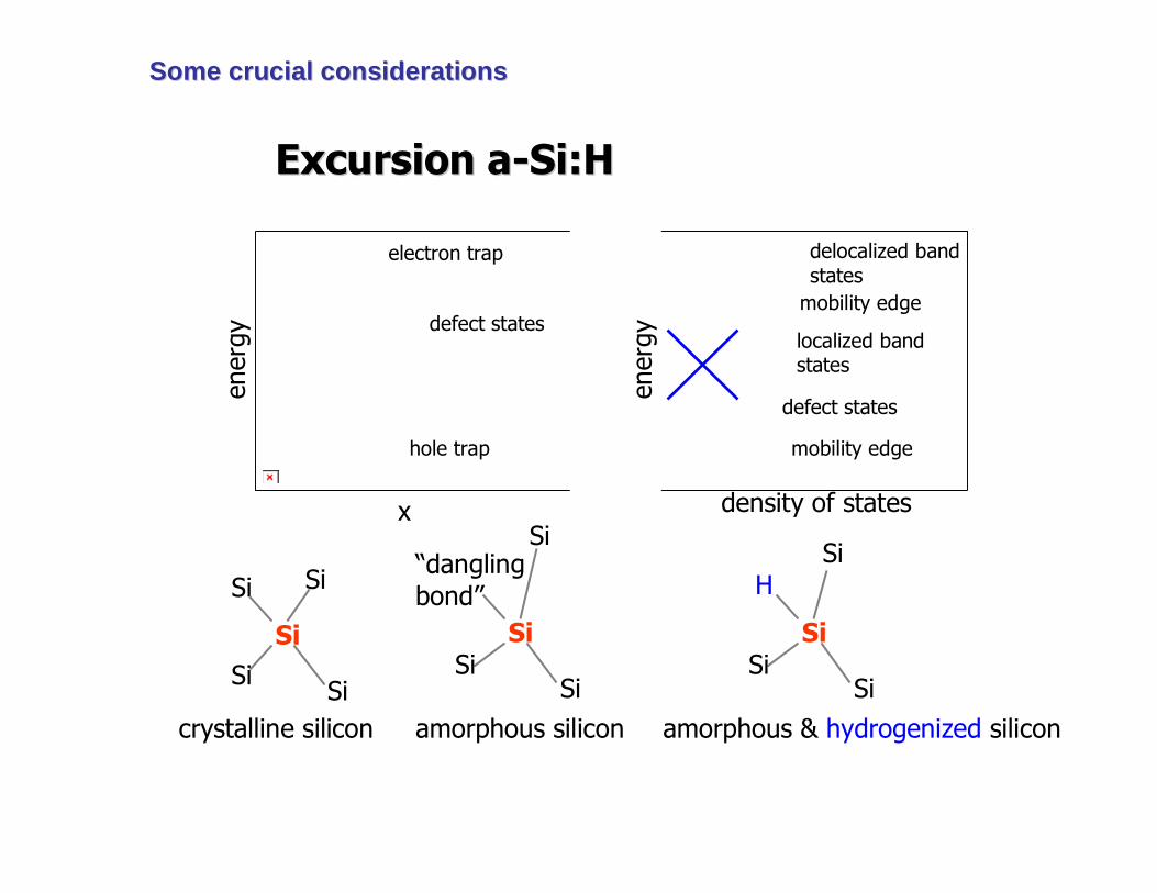
Excursion aExcursion a--Si:HSi:H
electron trap
defect states
hole trap
defect states
mobility edge
mobility edge
localized bandstates
delocalized bandstates
ener
gy
ener
gy
x density of states
Si
SiSi
SiSi
Si
SiSi
Si“danglingbond”
Si
SiSi
SiH
crystalline silicon amorphous silicon amorphous & hydrogenized silicon
Some crucial considerationsSome crucial considerations
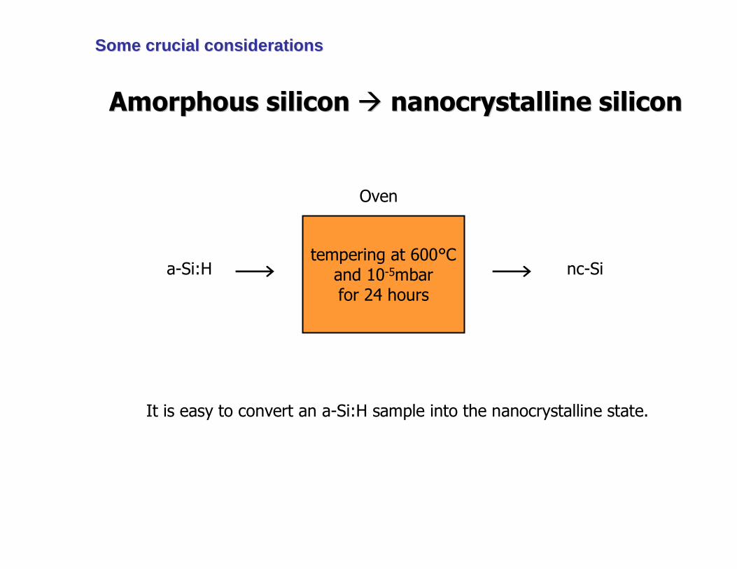
Amorphous silicon Amorphous silicon nanocrystallinenanocrystalline siliconsilicon
a-Si:Htempering at 600°C
and 10-5mbarfor 24 hours
nc-Si
Oven
It is easy to convert an a-Si:H sample into the nanocrystalline state.
Some crucial considerationsSome crucial considerations
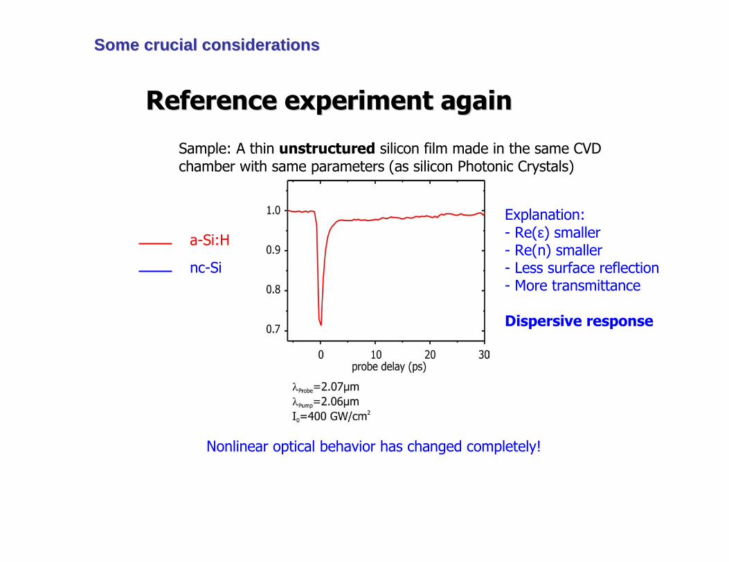
Reference experiment againReference experiment again
Sample: A thin unstructured silicon film made in the same CVD chamber with same parameters (as silicon Photonic Crystals)
Nonlinear optical behavior has changed completely!
a-Si:H
nc-Si
Explanation:- Re(ε) smaller- Re(n) smaller- Less surface reflection- More transmittance
Dispersive response
Some crucial considerationsSome crucial considerations
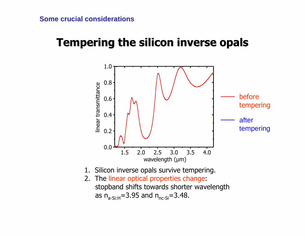
Tempering the silicon inverse opalsTempering the silicon inverse opals
1. Silicon inverse opals survive tempering.2. The linear optical properties change:
stopband shifts towards shorter wavelength as na-Si:H=3.95 and nnc-Si=3.48.
before tempering
after tempering
Some crucial considerationsSome crucial considerations
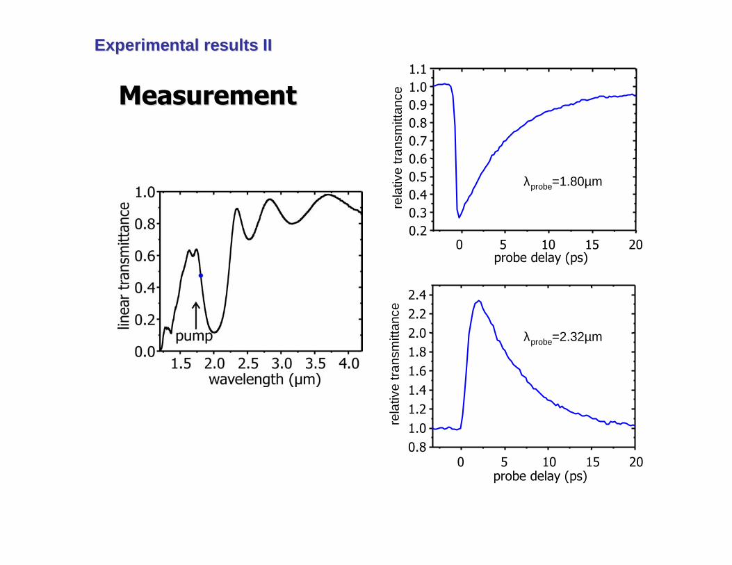
MeasurementMeasurement
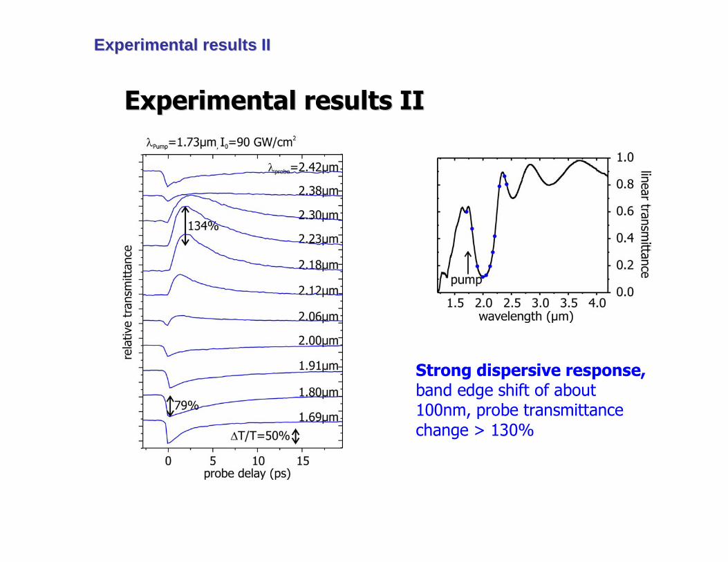
Experimental results IIExperimental results II
rela
tive
tran
smitt
ance
probe delay (ps)
λprobe=1.80µm
0 5 10 15 200.20.30.40.50.60.70.80.91.01.1
rela
tive
tran
smitt
ance
probe delay (ps)0 5 10 15 20
0.81.01.21.41.61.82.02.22.4
λprobe=2.32µm
Experimental results IIExperimental results II
Strong dispersive response,band edge shift of about100nm, probe transmittancechange > 130%
Experimental results IIExperimental results II
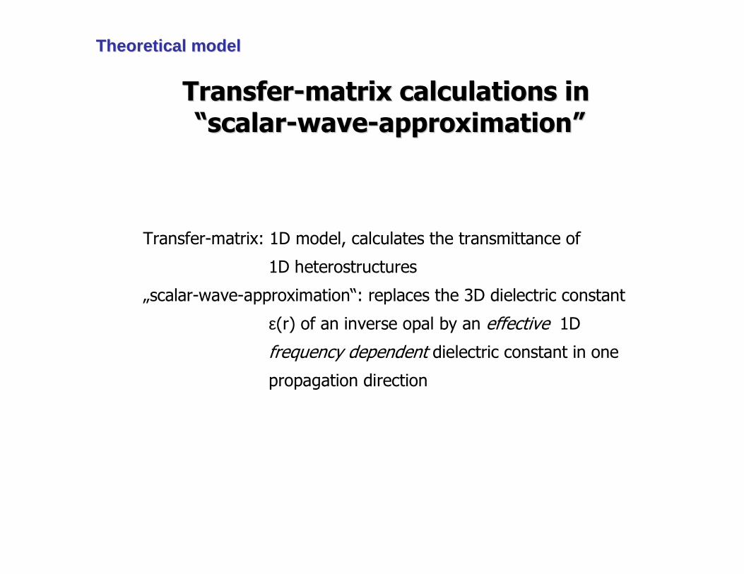
TransferTransfer--matrix calculations in matrix calculations in ““scalarscalar--wavewave--approximationapproximation””
Transfer-matrix: 1D model, calculates the transmittance of
1D heterostructures
„scalar-wave-approximation“: replaces the 3D dielectric constant
ε(r) of an inverse opal by an effective 1D
frequency dependent dielectric constant in one
propagation direction
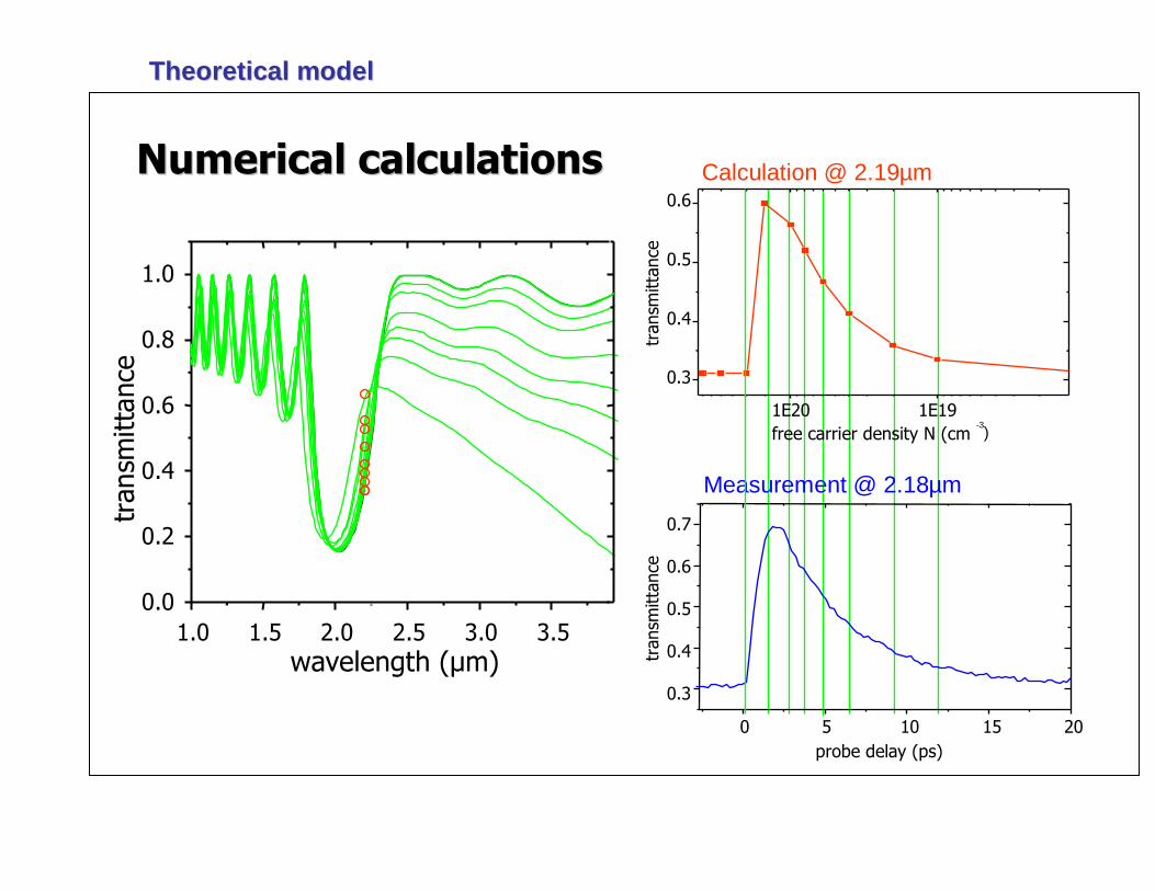
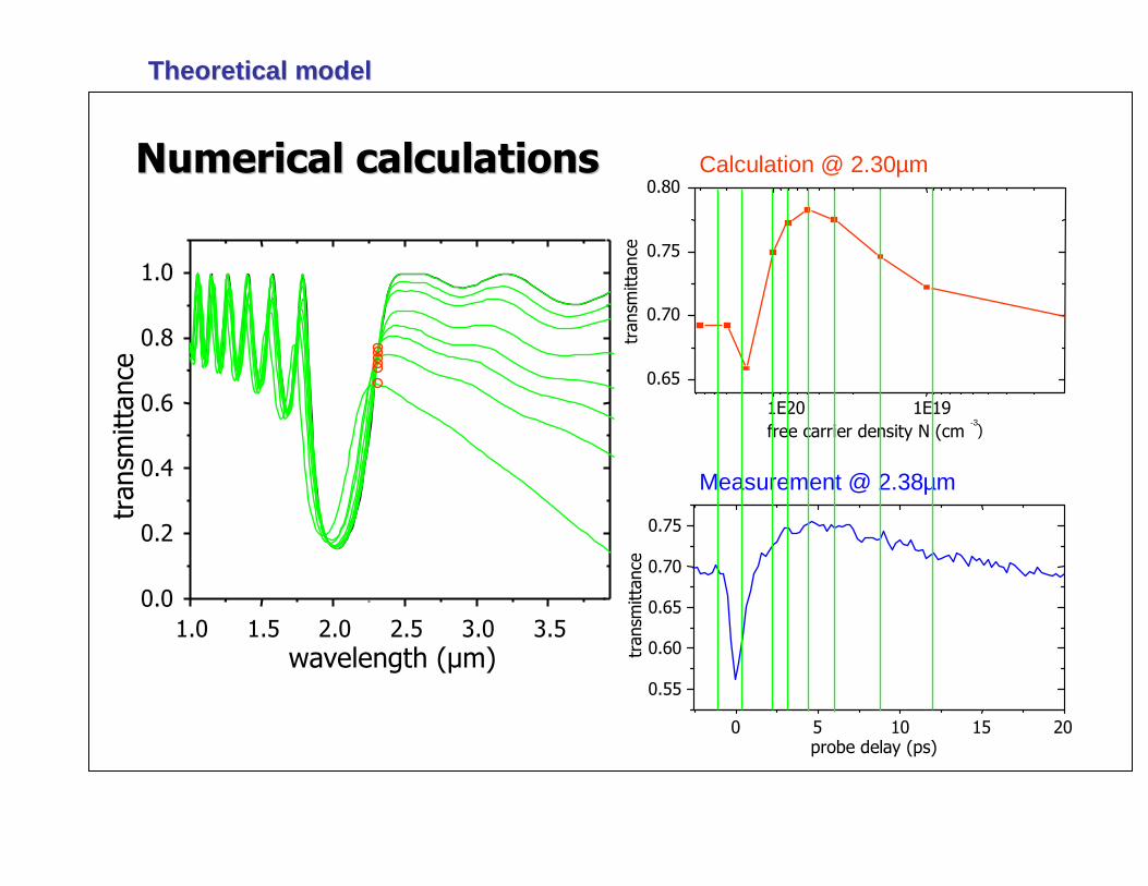
Theoretical modelTheoretical model
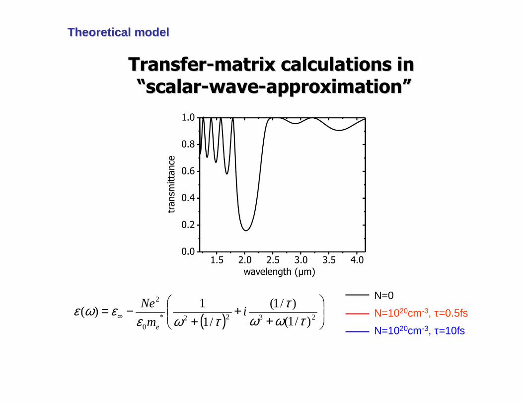
TransferTransfer--matrix calculations in matrix calculations in ““scalarscalar--wavewave--approximationapproximation””
N=0
N=1020cm-3, τ=0.5fs
N=1020cm-3, τ=10fs( )
+
++
−= ∞ 2322*0
2
)/1(
)/1(
/1
1)(
τωωτ
τωεεωε i
m
Ne
e
Theoretical modelTheoretical model
1.0 1.5 2.0 2.5 3.0 3.50.0
0.2
0.4
0.6
0.8
1.0
tran
smitt
ance
wavelength (µm) tran
smitt
ance
probe delay (ps)
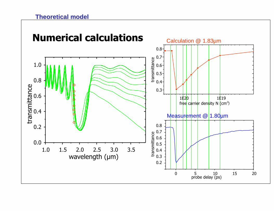
Numerical calculationsNumerical calculations Calculation @ 1.83µm
Measurement @ 1.80µm
tran
smitt
ance
1E20 1E19
0.3
0.4
0.5
0.6
0.7
0.8
free carrier density N (cm-3)
0 5 10 15 20
0.20.30.40.50.60.70.8
Theoretical modelTheoretical model
1.0 1.5 2.0 2.5 3.0 3.50.0
0.2
0.4
0.6
0.8
1.0
tran
smitt
ance
wavelength (µm)0.3
0.4
0.5
0.6
0.7
tran
smitt
ance
0 5 10 15 20probe delay (ps)
0.3
0.4
0.5
0.6
tran
smitt
ance
-31E20 1E19free carrier density N (cm )
Numerical calculationsNumerical calculations Calculation @ 2.19µm
Measurement @ 2.18µm
Theoretical modelTheoretical model
1.0 1.5 2.0 2.5 3.0 3.50.0
0.2
0.4
0.6
0.8
1.0
tran
smitt
ance
wavelength (µm) tran
smitt
ance
0 5 10 15 20probe delay (ps)
Numerical calculationsNumerical calculations Calculation @ 2.30µm
Measurement @ 2.38µm
tran
smitt
ance
-31E20 1E19free carrier density N (cm )
0.65
0.70
0.75
0.80
0.55
0.60
0.65
0.70
0.75
Theoretical modelTheoretical model