Embed Size (px)
Citation preview

warwick.ac.uk/lib-publications
Original citation: Donchev, Evgeniy, Pang, Jing S., Gammon, P. M., Centeno, Anthony, Xie, Fang, Petrov, Peter K., Breeze, Jonathan D., Ryan, Mary P., Riley, D. Jason and Alford, Neil McN.. (2014) The rectenna device : from theory to practice (a review). MRS Energy & Sustainability - A Review Journal, 1 . Permanent WRAP URL: http://wrap.warwick.ac.uk/62338 Copyright and reuse: The Warwick Research Archive Portal (WRAP) makes this work by researchers of the University of Warwick available open access under the following conditions. Copyright © and all moral rights to the version of the paper presented here belong to the individual author(s) and/or other copyright owners. To the extent reasonable and practicable the material made available in WRAP has been checked for eligibility before being made available. Copies of full items can be used for personal research or study, educational, or not-for profit purposes without prior permission or charge. Provided that the authors, title and full bibliographic details are credited, a hyperlink and/or URL is given for the original metadata page and the content is not changed in any way. Publisher’s statement: This article has been published in a revised form in http://dx.doi.org/10.1557/mre.2014.6 . This version is free to view and download for private research and study only. Not for re-distribution, re-sale or use in derivative works. © © Materials Research Society 2014 A note on versions: The version presented here may differ from the published version or, version of record, if you wish to cite this item you are advised to consult the publisher’s version. Please see the ‘permanent WRAP url’ above for details on accessing the published version and note that access may require a subscription For more information, please contact the WRAP Team at: [email protected]
The Rectenna Device - from theory to practice (a review)
E. Donchev,1, ∗ J. S. Pang,1 P. M. Gammon,2 A. Centeno,3 F. Xie,1
P. K. Petrov,1 J. Breeze,1 M. P. Ryan,1 D. J. Riley,1 and N. McN. Alford1
1Department of Materials, Imperial College London, London, SW7 2AZ, United Kingdom2School of Engineering, University of Warwick, Coventry, CV4 7AL, United Kingdom
3iKhoza Nano-Characterization, Structural Control and Processing,Malaysia-Japan International Institute of Technology, 54100 Kuala Lumpur, Malaysia
(Dated: April 20, 2014)
The Rectenna (RECTifying antENNA), which was first demonstrated by William C. Brown in1964 as a receiver for microwave power transmission, is now increasingly researched as a meansof harvesting solar radiation. Tapping into the growing photovoltaic market, the attraction of therectenna concept is the potential for devices that, in theory, are not limited in efficiency by theShockley-Queisser limit. In this review, the history and operation of this 40-year old device conceptis explored in the context of power transmission and the ever increasing interest in its potentialapplications at THz frequencies, through the infra-red and visible spectra. Recent modelling ap-proaches that have predicted controversially high efficiency values at these frequencies are criticallyexamined. It is proposed that to unlock any of the promised potential in the solar rectenna concept,there is a need for each constituent part to be improved beyond the current best performance, withthe existing nanometer scale antennas, the rectification and the impedance matching solutions allfalling short of the necessary efficiencies at THz frequencies. Advances in the fabrication, character-isation and understanding of the antenna and the rectifier are reviewed, and common solar rectennadesign approaches are summarised. Finally, the socio-economic impact of success in this field isdiscussed and future work is proposed.
I. INTRODUCTION
The ever increasing global demand for clean renew-able energy is a crucial topic that has major economicand societal impact for our future on this planet. Thesun is a constant source of energy, thus better harvest-ing its radiation would solve the energy challenge andhelp protect the environment. Conventional solar har-vesting is via the increasingly popular photovoltaic (PV)p-n junction solar cells. Although this field has seen greatimprovement over the last few decades since the first sil-icon solar cell was developed in 1941 at Bell Laborato-ries, its fundamental limitations discussed by Shockleyand Queisser1 in 1961 puts an upper boundary on theefficiency at around 30% for single junction solar cells1
and 55% for multi-junction solar cells2. Due to the effi-ciency limits of solar cells, other solar-energy convertingtechnologies are becoming increasingly attractive. An al-ternative solar energy converter concept is the Rectenna(RECTifying antENNA) device, which has achieved veryhigh efficiencies at microwave frequencies, while at THzfrequencies, it has been speculated that efficiencies ex-ceeding the Shockley-Queisser limit are achievable.
Fundamentally the Rectenna and the Solar Cell aresimilar as there is absorption of photons to generate aDC current. However, there is a substantial differencein their principles of operation. Solar cells are quantumdevices, except for their anti-reflection coatings, and areonly able to be understood and designed by the applica-
∗ Corresponding author:[email protected]
tion of quantum physics3, where light is perceived in itsparticle form, as photons. Hence, the efficiency is limitedby the band gap energy of the active layers, where energyis lost due to low energy photons passing right throughthe material, and through heat loss from the high fre-quency photons. The rectenna device concept is differ-ent as it is based upon the wave nature of light, which isregarded as a propagating, oscillating electric and mag-netic field4. Similar to a low pass filter in electronics,the efficient absorption of solar radiation is limited bythe cut-off frequency of the device, i.e. any wavelengthbelow this frequency can be harvested.
FIG. 1. Block diagram of microwave rectenna and load.(Reprinted from [3], c©2002 with permission from Elsevier)
The components of the rectenna device are shown inFigure 1. These components are commonly associatedwith a rectenna operating at microwave frequencies. Theantenna is used to capture and convert the energy froman incoming microwave beam (or solar radiation in thecase of solar rectenna) as it is an efficient transducer be-tween free space and guided waves5. The electric field(E) from an incident electromagnetic wave induces an
2
alternating current (AC) in the conducting antenna. Alow pass filter is used to form an impedance match be-tween the antenna and the rectifier, and passes the signalat the tuned operating frequency whilst blocking reradi-ation of higher order harmonic energy produced by therectifier3,6–8. The rectifier (a diode) converts the inputAC signal to a usable direct current (DC) which is trans-ferred to the load. A DC pass filter, consisting of aninductor in series, is used to smooth the rectified signalto DC whilst providing efficient transfer to the load.
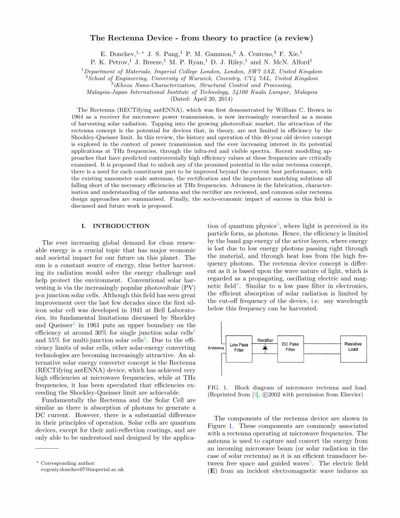
The antenna dimensions are of the same length scaleas the targeted frequency5. Therefore, for microwave fre-quencies, the antenna is relatively large (cm to mm scale)compared to that required for infrared (µm scale) andoptical frequencies (nm scale). Due to its smaller size,it will be difficult to incorporate the aforementioned fil-ters into the design of a rectenna for solar energy collec-tion. Therefore the components of the solar rectenna arereduced to just the Antenna and Rectifier (Figure 2)9.The removal of the low-pass filter from this design en-ables broadband frequency harvesting up to the cut-offfrequency of the device, although it introduces the diffi-culty of impedance matching the antenna and rectifier,resulting in a potential drop in efficiency. Losses in trans-ferring the rectified DC signal to the load are dependenton the diode behaviour. However, appropriate designof a DC pass filter would make its use possible in thisconfiguration99,100.
FIG. 2. Block diagram of solar rectenna and load. (Reprintedfrom [9], c©IOP Publishing. Reproduced by permission of IOPPublishing. All rights reserved.)
There are two families of designs for rectenna solarenergy collectors. Bailey10 proposed that each antennaelement is attached to its individual rectifier and the DCoutputs are combined (see Figure 5). The immediateconcern here is that the small voltage predicted fromthe antenna elements may be insufficient for rectifica-tion to occur in the attached diode element3. The onlyway to overcome this is to design a diode which turnson at a voltage as low as that arising from the singleantenna element. The other design is by Kraus11, whosuggested that the electrical oscillations from many an-
tenna elements be combined in a particular phase rela-tionship, then delivered together to the rectifier. Limita-tions in this design arise from the need for spatial coher-ence across all the antenna elements feeding the signal tothe diode3. This can be minimised by appropriate designand high quality fabrication of the antenna elements.
The aim of this article is to review key research in thedevelopment of the rectenna device as an alternative orin addition to conventional solar cell technology. We aimto expand upon a few short reviews, [3–5,9,100,105], thathave been published, bringing the reader up to date witha more detailed overview of the device. This article willbe the first to bring together all relevant research notonly on the rectenna as a whole device, but also the re-search on its two main components – the antenna andthe rectifier. The next section will briefly describe thehistory of the device and how the initial application ofmicrowave power transmission (MPT) was later modi-fied to a solar energy harvesting alternative. Section IIIwill analyse and discuss the many publications on ex-perimentally and theoretically derived device efficiencies.Breakthroughs in modelling and fabricating the antennaand rectifier will be reviewed in Section IV and V respec-tively. Section VI will bring together all components andlook at different rectenna architectures, which show po-tential for efficient operation at solar frequencies. We willdiscuss the socio-economic impact of the research in thisfield and proposed future work in Section VII before com-pleting the article with a short summary in Section VIII.
II. HISTORY OF THE RECTENNA DEVICE
The rectenna concept was initially proposed for wire-less power transmission by William C. Brown of theRaytheon Company in the 1960’s. At the time, Brown, apioneer of microwave power transmission, was faced witha challenge of how to efficiently receive and convert toDC power an incoming microwave beam. Wireless powertransmission was not a new concept as it had begun withthe ideas and demonstrations by Tesla in 1899 using ra-dio waves12. Tesla managed to demonstrate this conceptalthough never found an applicable route into its com-mercialisation.
In 1959 the Raytheon Company proposed theRaytheon Airborne Microwave Platform (RAMP) con-cept to the US Department of Defence as a solutionto communications and surveillance problems13. Thisproposed platform was to be flown at high altitude(50,000 ft) in the form of a helicopter, powered by mi-crowave transmission. The US Department of Defencedid not fund the project however the Raytheon Com-pany pursued their interest by researching the requiredtechnological developments for its realization. One miss-ing technology was a suitable microwave rectifier14, ca-pable of converting the microwave signal directly intothe DC current necessary to power the platform’s mo-tors and stay airborne. Their initial design used a
3
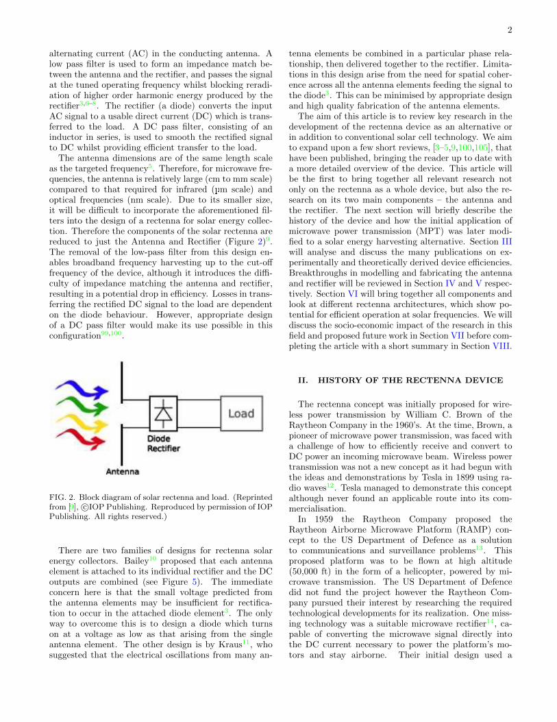
FIG. 3. Left: W.C. Brown holding the rectenna helicopter platform. Right: In flight demonstration of the rectenna helicopteron October 1964. (Reprinted from [17])
horn-illuminated ellipsoidal reflector that focused the mi-crowave beam into a trapezoidal horn at a 20 ft distancewhere the microwaves were converted to DC power by therectifier13. Using this first design, Brown constructed andflew thirty feet above his lawn a small tethered helicopterthat he had built with his son in his own workshop13.Although this concept worked, Brown was aware of theflaws in his system and continued to work on other pos-sibilities.
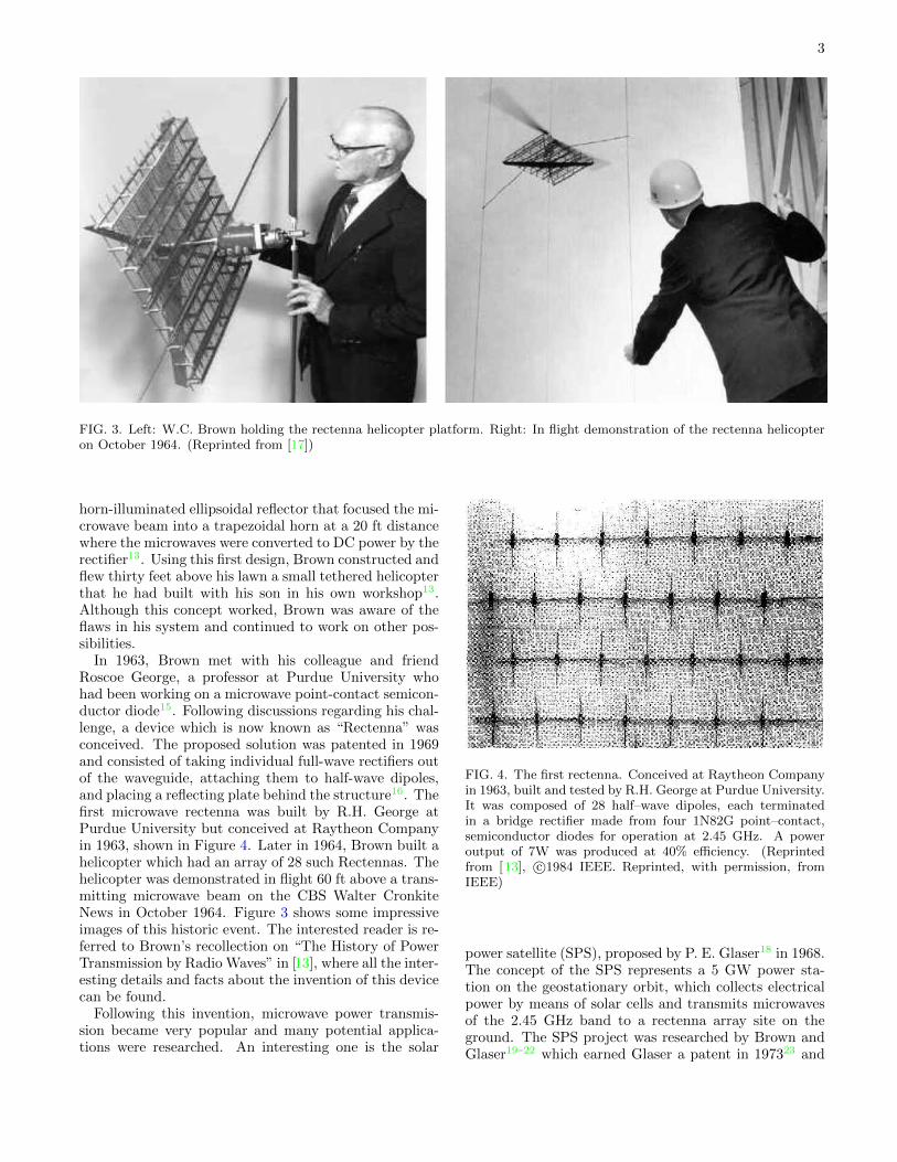
In 1963, Brown met with his colleague and friendRoscoe George, a professor at Purdue University whohad been working on a microwave point-contact semicon-ductor diode15. Following discussions regarding his chal-lenge, a device which is now known as “Rectenna” wasconceived. The proposed solution was patented in 1969and consisted of taking individual full-wave rectifiers outof the waveguide, attaching them to half-wave dipoles,and placing a reflecting plate behind the structure16. Thefirst microwave rectenna was built by R.H. George atPurdue University but conceived at Raytheon Companyin 1963, shown in Figure 4. Later in 1964, Brown built ahelicopter which had an array of 28 such Rectennas. Thehelicopter was demonstrated in flight 60 ft above a trans-mitting microwave beam on the CBS Walter CronkiteNews in October 1964. Figure 3 shows some impressiveimages of this historic event. The interested reader is re-ferred to Brown’s recollection on “The History of PowerTransmission by Radio Waves” in [13], where all the inter-esting details and facts about the invention of this devicecan be found.
Following this invention, microwave power transmis-sion became very popular and many potential applica-tions were researched. An interesting one is the solar
FIG. 4. The first rectenna. Conceived at Raytheon Companyin 1963, built and tested by R.H. George at Purdue University.It was composed of 28 half–wave dipoles, each terminatedin a bridge rectifier made from four 1N82G point–contact,semiconductor diodes for operation at 2.45 GHz. A poweroutput of 7W was produced at 40% efficiency. (Reprintedfrom [13], c©1984 IEEE. Reprinted, with permission, fromIEEE)
power satellite (SPS), proposed by P. E. Glaser18 in 1968.The concept of the SPS represents a 5 GW power sta-tion on the geostationary orbit, which collects electricalpower by means of solar cells and transmits microwavesof the 2.45 GHz band to a rectenna array site on theground. The SPS project was researched by Brown andGlaser19–22 which earned Glaser a patent in 197323 and
4
a collaborative three year project together with Brownin 1977 called the “DOE/NASA Satellite Power SystemConcept Development and Evaluation Program”. Thework ended in 1980 with much success in developingnew ideas in the design of transmission technology andrectenna arrays however did not attract further funding.Although this was the end of the SPS initiative in the US,some experimental studies of the concept were seen in the1990s in Yamasaki, Japan24,25. The interested reader isreferred to Glaser’s overview of SPS progress in [26].
The developments from the SPS project yieldedother applications involving microwave transmission andrectenna, such as intersatellite power transmission27, in-cluding utility power satellites28, mechanical actuatorsfor space-based telescopes29, small dc motor driving30,short range power transfer as for example between twoparts of a satellite, RF identification tags (RFID) andbiomedical implants31. These applications all includesingle band rectenna operation. Hagerty et al31 haveshown a broadband rectenna array for microwave opera-tion to be used in low-power indoor sensor networks andRF energy recycling. Recent publications have shown acompact printed rectenna that can be used to supply DCpower to electrical devices supporting data communica-tion systems32.
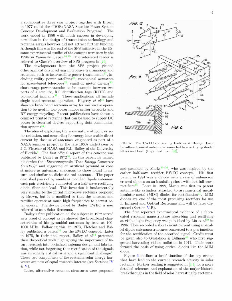
The idea of exploiting the wave nature of light, or so-lar radiation, and converting its energy into usable directcurrent by the use of antennas, originated as part of aNASA summer project in the late 1960s undertaken byJ.C. Fletcher of NASA and R.L. Bailey of the Universityof Florida4. The first official report of this concept waspublished by Bailey in 197210. In this paper, he namedhis device the “Electromagnetic Wave Energy Converter(EWEC)” and suggested an artificial pyramid or conestructure as antennas, analogous to those found in na-ture and similar to dielectric rod antennas. The paperdescribed pairs of pyramids as modified dipole antennas,each pair electrically connected to a half-wave rectifyingdiode, filter and load. This invention is fundamentallyvery similar to the initial microwave rectenna proposedby Brown, but it is modified so that the antenna andrectifier operate at much high frequencies to harvest so-lar energy. The device called by Bailey EWEC is nowreferred to as a Solar Rectenna.
Bailey’s first publication on the subject in 1972 servedas a proof of concept as he showed the broadband char-acteristics of his pyramidal antennas by tests at 100-1000 MHz. Following this, in 1973, Fletcher and Bai-ley published a patent33 on the EWEC concept. Laterin 1975, in their final report, Bailey et al34 presentedtheir theoretical work highlighting the importance of fu-ture research into optimised antenna design and fabrica-tion, while not forgetting that rectification of the signalswas an equally critical issue and a significant challenge4.These two components of the rectenna solar energy har-vester are now of equal research interest (see Sections IV& V).
Later, alternative rectenna structures were proposed
FIG. 5. The EWEC concept by Fletcher & Bailey. Eachbroadband conical antenna is connected to a rectifying diode,filters and load. (Reprinted from [33])
and patented by Marks35–38, who was inspired by theearlier half-wave rectifier EWEC concept. His firstpatent in 1984 was a device with arrays of submicroncrossed dipoles on an insulating sheet with fast full-waverectifiers35. Later in 1988, Marks was first to patentantenna-like cylinders attached to asymmetrical metal-insulator-metal (MIM) diodes for rectification37. MIMdiodes are one of the most promising rectifiers for usein Infrared and Optical Rectennas and will be later dis-cussed (Section V.B).
The first reported experimental evidence of a fabri-cated resonant nanostructure absorbing and rectifyingat visible light frequency was published by Lin et al39 in1996. They recorded a short circuit current using a paral-lel dipole sub-nanostructures connected to a p-n junctionfor the rectification of the absorbed signal. Credit mustbe given also to Gustafson & Billman40 who first sug-gested harvesting visible radiation in 1974. Their workformed the basis of using optical diodes like the MIMdiode.
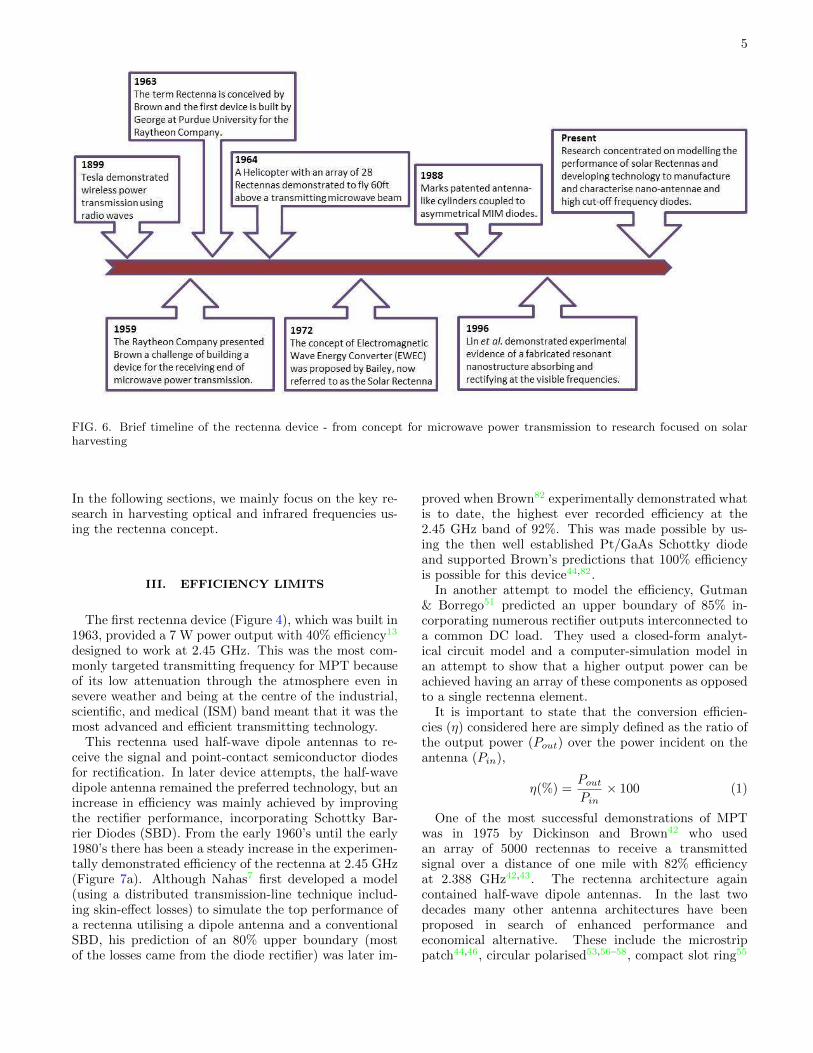
Figure 6 outlines a brief timeline of the key eventsthat have lead to the current research activity in solarrectenna. Further reading is suggested in [3,4] for a moredetailed reference and explanation of the major historicbreakthroughs in the field of solar harvesting by rectenna.
5
FIG. 6. Brief timeline of the rectenna device - from concept for microwave power transmission to research focused on solarharvesting
In the following sections, we mainly focus on the key re-search in harvesting optical and infrared frequencies us-ing the rectenna concept.
III. EFFICIENCY LIMITS
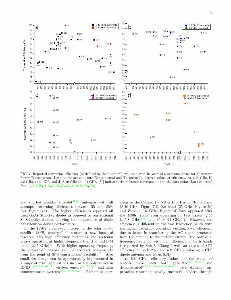
The first rectenna device (Figure 4), which was built in1963, provided a 7 W power output with 40% efficiency13
designed to work at 2.45 GHz. This was the most com-monly targeted transmitting frequency for MPT becauseof its low attenuation through the atmosphere even insevere weather and being at the centre of the industrial,scientific, and medical (ISM) band meant that it was themost advanced and efficient transmitting technology.
This rectenna used half-wave dipole antennas to re-ceive the signal and point-contact semiconductor diodesfor rectification. In later device attempts, the half-wavedipole antenna remained the preferred technology, but anincrease in efficiency was mainly achieved by improvingthe rectifier performance, incorporating Schottky Bar-rier Diodes (SBD). From the early 1960’s until the early1980’s there has been a steady increase in the experimen-tally demonstrated efficiency of the rectenna at 2.45 GHz(Figure 7a). Although Nahas7 first developed a model(using a distributed transmission-line technique includ-ing skin-effect losses) to simulate the top performance ofa rectenna utilising a dipole antenna and a conventionalSBD, his prediction of an 80% upper boundary (mostof the losses came from the diode rectifier) was later im-
proved when Brown82 experimentally demonstrated whatis to date, the highest ever recorded efficiency at the2.45 GHz band of 92%. This was made possible by us-ing the then well established Pt/GaAs Schottky diodeand supported Brown’s predictions that 100% efficiencyis possible for this device44,82.
In another attempt to model the efficiency, Gutman& Borrego51 predicted an upper boundary of 85% in-corporating numerous rectifier outputs interconnected toa common DC load. They used a closed-form analyt-ical circuit model and a computer-simulation model inan attempt to show that a higher output power can beachieved having an array of these components as opposedto a single rectenna element.
It is important to state that the conversion efficien-cies (η) considered here are simply defined as the ratio ofthe output power (Pout) over the power incident on theantenna (Pin),
η(%) =PoutPin
× 100 (1)
One of the most successful demonstrations of MPTwas in 1975 by Dickinson and Brown42 who usedan array of 5000 rectennas to receive a transmittedsignal over a distance of one mile with 82% efficiencyat 2.388 GHz42,43. The rectenna architecture againcontained half-wave dipole antennas. In the last twodecades many other antenna architectures have beenproposed in search of enhanced performance andeconomical alternative. These include the microstrippatch44,46, circular polarised53,56–58, compact slot ring55
6
FIG. 7. Reported conversion efficiency (as defined by their authors) evolution over the years of a rectenna device for MicrowavePower Transmission. Data points are split into Experimental and Theoretically derived values of efficiency. a) 2.45 GHz, b)5.8 GHz, c) 35 GHz and d) 8-10 GHz and 94 GHz. [**] indicates the reference corresponding to the data point. Data collectedfrom [3,5–7,10,11,13,25,28,29,32,41–51,53–82,101]
and shorted annular ring-slot47,53 antennas with allattempts returning efficiencies between 55 and 85%(see Figure 7a). The higher efficiencies reported allused GaAs Schottky diodes as opposed to conventionalSi Schottky diodes, showing the importance of diodebehaviour on device performance.
In the 1990’s a renewed interest in the solar powersatellite (SPS) concept18–26 started a new focus ofresearch into high efficiency rectennas and rectennaarrays operating at higher frequency than the mid-ISMband (2.45 GHz)41. With higher operating frequency,the device dimensions can be reduced convenientlyfrom the point of SPS construction feasibility41. Alsosmall size design can be appropriately implemented ina range of other applications such as a supply source inRFID31,55,58,64,68,77, wireless sensors31,47,58,77 and datacommunication systems32,61,64,65,67,77. Rectennas oper-
ating in the C-band (≈ 5.8 GHz – Figure 7b), X-band(8-10 GHz Figure 7d), Kα-band (35 GHz Figure 7c)and W-band (94 GHz Figure 7d) have appeared afterthe 1990s, some even operating in two bands (2.45& 5.8 GHz53–55 and 35 & 94 GHz77). However, theefficiency is different in the two frequency bands withthe higher frequency operation yielding lower efficiencydue to losses in transferring the AC signal generatedfrom the antenna to the rectifier circuit. The only dualfrequency rectenna with high efficiency in both bandsis reported by Suh & Chang54 with an excess of 82%efficiency at both 2.45 and 5.8 GHz employing a CPSdipole antenna and GaAs SBD.
At 5.8 GHz, efficiency values in the range of60-85% have been both predicted6,61,67,68 anddemonstrated6,32,54,59–63,65,66,69–72 with different ap-proaches returning equally successful devices through
7
the years (Figure 7b). The few experimentally reportedrectennas at 8-10 GHz have seen slight improvementin efficiency when a circular or dual polarised printedpatch antenna has been coupled to the GaAs28,29 or Si73
Schottky diode, however with a planar slot antenna74
the efficiency is only 21.2% (Figure 7d). At 35 GHz (seeFigure 7c) theoretical predictions are higher than theircorresponding experimental results28,44, although witha similar antenna and diode design, high experimentalefficiency of 70% has been reported elsewhere [ 79,81].Analysis of the different efficiencies achieved with similarrectenna technologies highlight the importance in thecircuit and device design for rectennas used in microwavepower transmission. Furthermore, load impedance andthe power of the incoming beam also affect the overallefficiency of the device.
It can be noticed from Figure 7 that for a givenfrequency some models predict a lower efficiency thanthat which had already been experimentally achieved.The reason is that over the years, new antenna andrectifier technologies, and alternative, more compactcircuit designs were emerging, which could not improveor even match the record efficiency achieved with thehalf-wave dipole antenna and Pt/GaAs SBD. Further-more, scaling down the components and aiming towardshigher frequency operation at lower cost, introduceddifficulties for appropriate circuit design and the effi-ciency suffered a continuous drop. Overall, consideringthe evolution of reported efficiencies over the years(Figure 7) for MPT rectennas, it can be concluded thatwith appropriate antenna design, good matching to asuitable well-functioning diode rectifier connected to aDC load, experimental evidence of efficiencies over the70% mark can be obtained for frequencies up to 35 GHz(see also Figure 8).
The high efficiencies achieved at the low GHz frequen-cies are due to the ease of fabricating the devices anddesigning appropriate filters (low pass and DC pass – seeFigure 1). To be able to receive a signal, the antenna hasto be of the same length scale as the wavelength of theincoming wave, which at the low GHz frequencies rangesfrom a few mm to 10’s of cm. At infrared and opticalfrequencies, wavelengths are from µm to nm, which sub-sequently indicates the necessity of building the antennaand rectifier in this length scale range. At this scale, adirect impedance match of the antenna to rectifier has tobe achieved (Figure 2) instead of using a low-pass filter,which cannot be designed at such small dimensions.This is what Bailey’s proposed electromagnetic waveenergy converter10 implies – a scaled down version ofBrown’s rectenna consisting of a µm length antennaconnected directly to the diode rectifier transferring theoutput to the load through a DC pass filter of some sort.Bailey predicted an efficiency in excess of 50% for hisEWEC device at microwave frequencies, although notbacked by any modelling or experimental evidence of awhole device. The only evidence he gives is the abilityof an EWEC prototype to absorb electromagnetic plane
polarized waves at 475 MHz. His vision was to studythe concept at microwaves and later scaling it to lightfrequencies where he speculates potential for unity effi-ciency. A MPT rectenna device without a low-pass filteris possible and was demonstrated in 2012 at 2.45 GHz47.The proposed printed shorted annular ring-slot rectennais designed to match the impedance of the SBD rectifierat 2.45 GHz. The diode however will produce secondand third order harmonics which will re-radiate at 4.9and 7.35 GHz but these will be blocked because theantenna is designed to mismatch its impedance at thehigher order harmonics thus preventing re-radiation47.This device architecture removes the need for a low-passfilter design and achieves 69% efficiency.
Apart from Brown45,82 (for microwave) and Bailey10
(for solar) several other authors (Kraus11, Balanis86,and Andersen & Frandsen107) have speculated aboutthe possibility of 100% conversion efficiency comingfrom highly absorptive no-loss antennas and idealmatching, transferring and rectification of the absorbedinput signal to the load. This antenna efficiency isassuming uniform distribution of energy across theantenna, a single frequency and a coherent source. Thehigh efficiency values for MPT are achieved not onlywith appropriate antenna design, matching circuit andrectifier performance, but also with efficient delivery ofa good signal, because the artificially created microwavesignal is single band, polarised and coherent. Thismakes the antenna engineering easier. Simply reducingthe size of the components to operate at solar frequen-cies does not necessary mean that the efficiency willremain as high as that observed for MPT Rectennas.Unlike monochromatic microwave radiation, sunlightis unpolarised, incoherent and distributed over a wideband of wavelengths96. This creates further challengesin antenna engineering and lead to disputes on how tomodel the device performance. Furthermore, the diodehas to be optimised to rectify the signal at the higherfrequencies and both antenna and diode have to be wellmatched to maximise power transfer.
Provisional tests at 10 GHz with a dipole antenna anda Schottky diode were demonstrated by ITN5 estimatingefficiencies of over 50% however this frequency is toolow for solar energy harvesting. ITN state that thelower frequency rectenna is scalable to the higher THzfrequencies required for solar harvesting with theirmodels predicting up to 85%5 efficiency. According tomicrowave antenna theory, the antenna length scaleslinearly with the incident frequency which means thatin theory the antenna can be scaled to resonate at IRand optical frequencies5. This is not entirely the casebecause at IR and optical frequencies the conduction isnot Ohmic and the scaling laws are rather an estimationthan an accurate representation of the real-life situationas the majority of the energy in the surface modes is car-ried in the dielectric above the antenna. This symbolisesthe importance of impedance losses. The antenna hasto be designed to resonate against a complex waveform
8
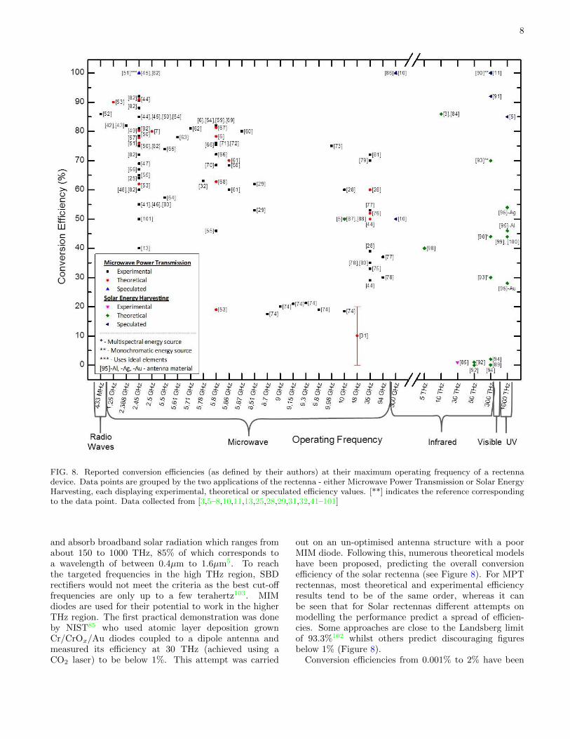
FIG. 8. Reported conversion efficiencies (as defined by their authors) at their maximum operating frequency of a rectennadevice. Data points are grouped by the two applications of the rectenna - either Microwave Power Transmission or Solar EnergyHarvesting, each displaying experimental, theoretical or speculated efficiency values. [**] indicates the reference correspondingto the data point. Data collected from [3,5–8,10,11,13,25,28,29,31,32,41–101]
and absorb broadband solar radiation which ranges fromabout 150 to 1000 THz, 85% of which corresponds toa wavelength of between 0.4µm to 1.6µm5. To reachthe targeted frequencies in the high THz region, SBDrectifiers would not meet the criteria as the best cut-offfrequencies are only up to a few terahertz103. MIMdiodes are used for their potential to work in the higherTHz region. The first practical demonstration was doneby NIST85 who used atomic layer deposition grownCr/CrOx/Au diodes coupled to a dipole antenna andmeasured its efficiency at 30 THz (achieved using aCO2 laser) to be below 1%. This attempt was carried
out on an un-optimised antenna structure with a poorMIM diode. Following this, numerous theoretical modelshave been proposed, predicting the overall conversionefficiency of the solar rectenna (see Figure 8). For MPTrectennas, most theoretical and experimental efficiencyresults tend to be of the same order, whereas it canbe seen that for Solar rectennas different attempts onmodelling the performance predict a spread of efficien-cies. Some approaches are close to the Landsberg limitof 93.3%102 whilst others predict discouraging figuresbelow 1% (Figure 8).
Conversion efficiencies from 0.001% to 2% have been
9
theoretically derived89,92,94 employing various assump-tions and a variation of modelling approaches (Figure 8).Mashaal & Gordon89 analysed the efficiency in termsof losses by the state-of-art rectenna designs whichadopt single polarization antennas able to convert onlyhalf of the random-polarization input power from solarradiation and a half-wave rectifier blocking the negativevoltages of the input signal. Their assumptions werebased on ideal matching between antenna and rectifier,zero turn-on voltage, limitless switching speeds and non-filtered signal output from the antenna prior to enteringthe rectifier which yielded an overall conversion efficiencyof 0.0795% and four times as high if a full-wave rectifieris employed. It is a common misperception that withrectennas, the diode forms a half-wave rectifier, whichwould hold true for a single diode in a series configura-tion. However, common rectenna design incorporates adiode connected in parallel, which forms a clamp circuitcapable of rectifying the full wave99,100. Therefore,estimating rectenna conversion efficiency should notbe discouraged by assuming a half-wave rectificationmechanism. Instead, efforts should be concentratedin understanding the effect of impedance mismatch.Briones et al.92 based their model on the assumptionthat the collection of EM radiation by the antenna isdone efficiently, which resulted in 0.001% efficiency ofthe system due to impedance mismatch losses betweenantenna and rectifier and inefficient rectification of thesignal. By assuming efficient rectifier performance, thepotential efficiency rises to approximately 1%.
An equally important criterion for efficient deviceoperation is antenna material selection. Vandenbosch& Ma divided the analysis on the efficiency of nano-rectennas into two parts – 1) the efficiency by whichthe light is captured by the antenna and brought to itsterminals97 and 2) the efficiency by which the capturedlight is transformed to low frequency power by thediode95,96. Considering first the antenna efficiency, theystudied various antenna materials in the form of 250 nmdipoles placed on a substrate97. Their calculationspredicted antenna efficiency of 61.6% for Ag, 50.3% forAl, 34.3% for Au, 29.5% for Cu and 9.4% for Cr. Ina later paper, [95], they looked at the diode efficiencyand more specifically, investigated the power loss dueto impedance matching whilst assuming efficient signalrectification. This analysis was only done on the highestperforming materials – Ag, Al and Au. Their workwas a continuation of a previous work by Sarehraz etal.96, however their analysis covered 75% of the powerradiated by the sun (up to 1000 THz) whereas Sarehrazet al. only based their analysis on 15% of the spectrum.Although Al gave the best matching efficiency of 97%,the best overall conversion efficiency of the rectennaconsidering both constituent parts is with Ag whichgives 54% whereas Al would have 46% and Au just28%95(Figure 8). So far the analysed publications allshare a united opinion that a suitable rectifier is neededin order for the above mentioned efficiency estimates
to be achieved or improved. For impedence matching,Ma & Vandenbosch95 suggest that the impedance of therectifier must be of the order of 100Ω both for the realand imaginary part and favour aluminium as being asuitable material for this application.
A governing factor in rectifier performance is its RCtime constant which defines the cut-off frequency, fc.This is the upper limit at which the rectification processis efficient. Above the cut-off frequency, rectificationis still possible however the strength of the rectifiedsignal at the output of the MIM will drop by a factorof approximately (fc)
2, thus the higher the frequencyabove fc the lower the rectification efficiency96. Thecut-off frequency is estimated by the following expressionproposed by Sanchez et al.104,
fc =1
2πRC(2)
where R is the series resistance and C is the capacitance.The cut-off frequency of the whole rectenna device can beevaluated by the following relation, which considers theantenna impedance (RA) and diode resistance (RD)92,
f c =RA +RD
2πRARDCD(3)
To achieve a high cut-off frequency, the RC constantmust be small, which can be obtained with a small junc-tion area104, and appropriate material selection and fab-rication. MIM rectifiers, although the most promisingrectifier technology, have not been demonstrated at highTHz frequencies with the best MIM diodes operating onlyup to 150 THz (λ = 2 µm)5 (more detail in Section V).Improving MIM fabrication technology and material sys-tem design would potentially yield the solution to therectenna efficiency.
So far, the reviewed efficiencies were all based on clas-sical approaches, not concerning thermodynamic limitsto solar energy conversion. In terms of equilibrium, anantenna receiving power from any source and transferringit to the load must transmit the same amount of powerback to the source3. If the power is extracted from theload, the reduction in its temperature will introduce adifferent approach to analysing the energy balance be-tween the incoming, extracted and reradiated powers. Inthis case, Corkish et al.3 state that the system wouldhave the same conversion efficiency limit as the one ex-pected for a solar thermal collector. Assuming the Sunto be a 6000 K black body and the surroundings to beat 300 K, this limit is 85.4% for mono-spectral energyconversion and 86.8% for multi-spectral. Further analy-sis suggests that the Landsberg102 limit of 93.3% can bereached due to certain benefits that the rectifying diodeshave in rectennas (see [3] for more details), however thisis hard to justify due to the generation of thermal noiseby the rectifiers. Diodes cannot rectify their own ther-mal noise as it violates the second law of thermodynamics(known as Brillouin’s paradox106).
Lerner et al.93 developed a thermodynamic expression
10
for the open circuit voltage and conversion efficiencyof a rectenna with the rectification process based onthe geometric property of the antenna tip which pro-vides a connection to the circuit and creates a tunneljunction. They envisioned the possibility of using ad-vanced nanofabrication techniques and a selective atomiclayer deposition process to manufacture nanometer junc-tions which would potentially allow for rectification ofblue light frequencies93. In modelling the circuit of therectenna, it can either be considered as a constant volt-age source with an emf independent of the load resis-tance or as a constant current source whose emf dependson the load resistance. As suggested by Lerner et al.93,the rectenna device is more appropriately modelled as aconstant current source in which case efficiencies are pre-dicted in excess of 70% for a monochromatic light sourceand an optimised device. Should the device be tunedfor multiphoton absorption, the efficiencies are expectedto be further enhanced93. The question remains as towhether a suitable technology is yet available to makesuch structures.
Another analysis on the broadband blackbody radia-tion response of optical rectennas was done by Joshi &Moddel90 by using the theory of photon assisted tun-nelling. By assuming negligible reverse current of thediode, zero dark current turn-on voltage and perfectmatching to the antenna, the device power conversionefficiency at monochromatic light can approach 100%,whereas for multispectral light the value is approachinga maximum at 44% at an operating voltage of 1.1 V.It should be noted that these authors also suggest thatspectral splitting is likely to improve the efficiency. Thiscan be achieved by setting the operating voltage for eachrectenna to rectify the desired spectral range, thus imply-ing that the operating voltage for the diodes in rectennashas a similar role to the band-gap as a limiting factor inphotovoltaic devices90.
With its proven success to receive and rectifymonochromatic microwave beams with high efficiency,there is a growing interest in establishing the true poten-tial of the rectennas’ ability to convert solar radiation. Asseen in Figure 8, there are many theoretical approachespredicting this, however there is no one universal theorythat clearly states whether the solar rectenna can com-pete with, let alone surpass common photovoltaic cells.There is however, the common opinion between scien-tists worldwide that the technology is not mature enoughto fabricate a device of comparable efficiency. Advancesin antenna engineering suggest that it is now possibleto manufacture nano sized antennas which can absorbsolar radiation from the infrared to the visible frequen-cies (Section IV). Work on the rectifier component hasseen great progress over the years with many attemptsshowing great potential for use in rectenna devices (Sec-tion V).
IV. ANTENNA
Antennas are used either as transmitters, to createelectromagnetic (EM) waves that have a well-defined ra-diation pattern, or as receivers of EM waves from a re-mote source86. The purpose is usually to send or extractinformation that is encoded into the EM wave. Anten-nas are now essential in many aspects of modern dayliving, the mobile phone being the most common exam-ple. They normally operate at a resonance. Typicallythis is a half wavelength dipole antenna. The resonantwavelength of the antenna will be at the wavelength ofthe incoming propagating signal and energy is then trans-ferred between them. For this reason, the antennas areusually fabricated in the dimensions of the wavelengthof the incident wave. A higher frequency thus requiresa smaller antenna. However, an antenna designed to beresonant at a very specific frequency by only consideringa linear dimension does not guarantee efficient energy ab-sorption. Other factors such as impedance mismatch inthe circuits, bandwidth, direction and polarisation of in-cidence radiation needs to be considered. The aim of thissection is to introduce some different designs of antennasfor microwave and optical frequencies.
Most antennas at microwave frequencies are designedto work within a specific frequency band reserved forindustrial, scientific and medical (ISM) frequency use.For example, one of the most popular frequency bands is2.4 – 2.5 GHz, which devices such as wireless networks,near-field communications, and Bluetooth use. There-fore these antennas only require millimeter dimension. Adipole antenna is one of the simplest designs. It con-sists of two identical metal elements in mirror symmetry.The most common form is two metal rods aligned on thesame axis. The length of the metal rods is half the size ofthe resonance wavelength. Higher-order resonance modesalso occur in the same antenna but at reduced efficiencydue to attenuation of the induced current in the antenna.Nevertheless, the accepted frequency bandwidth is verynarrow. A slight variation of the incoming frequencygives rise to parasitic capacitance and inductance result-ing in inefficient energy absorption. Therefore, a precisefabrication of the antenna is necessary. This increasesthe difficulty in manufacturing good devices, especiallywhen the frequency of interest is higher.
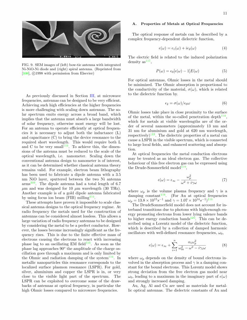
One method to circumvent the narrowband absorptionproblem, which dipole antennas encounter is to extendthe arms width above the standard limit (i.e. 5% longerthan the wavelength)108, allowing a bigger window of fre-quency acceptance. This type of antenna is referred to asthe bow-tie antenna (Figure 9). The length of each armis half the size of the radiation of interest. However, thecorrect length of the antenna alone does not guaranteehigh efficiency absorption since the incoming wave hasvarious angles of incidence and polarisation109. To over-come this problem, a variety of designs have been investi-gated, such as spiral108,110(Figure 9), log-periodic108,110,microstrip slot111, and retrodirective rectenna array112.
11
FIG. 9. SEM images of (left) bow-tie antenna with integratedNi-NiO-Ni diode and (right) spiral antenna. (Reprinted from[108], c©1998 with permission from Elsevier)
As previously discussed in Section III, at microwavefrequencies, antennas can be designed to be very efficient.Achieving such high efficiencies at the higher frequenciesis more challenging with scaling down antennas. The so-lar spectrum emits energy across a broad band, whichimplies that the antenna must absorb a large bandwidthof solar frequency, otherwise most energy will be lost.For an antenna to operate efficiently at optical frequen-cies it is necessary to adjust both the inductance (L)and capacitance (C) to bring the device resonance to therequired short wavelength. This would require both Land C to be very small113. To achieve this, the dimen-sions of the antenna must be reduced to the scale of theoptical wavelength, i.e. nanometer. Scaling down theconventional antenna design to nanometer is of interest,as it can be determined whether classical antenna theoryremains valid. For example, electron beam lithographyhas been used to fabricate a dipole antenna with a 3.5nm NiO layer, sputtered between the two Ni antennaarms109. The dipole antenna had a total length of 6.7µm and was designed for 10 µm wavelength (30 THz).Another example is of a gold dipole antenna fabricatedby using focus ion beam (FIB) milling114.
These attempts have proven it impossible to scale clas-sical antenna designs to the optical frequency regime. Atradio frequency the metals used for the construction ofantennas can be considered almost lossless. This allows alarge variation of radio frequency antennas to be designedby considering the metal to be a perfect conductor. How-ever, the losses become increasingly significant as the fre-quency rises. This is due to the finite effective mass ofelectrons causing the electrons to react with increasingphase lag to an oscillating EM field115. As soon as thephase lag approaches 90o the amplitude of the charge os-cillation goes through a maximum and is only limited bythe Ohmic and radiation damping of the system116. Inmetallic nanoparticles this resonance corresponds to thelocalized surface plasmon resonance (LSPR). For gold,silver, aluminium and copper the LSPR is in, or veryclose to the visible light part of the spectrum. TheLSPR can be exploited to overcome some of the draw-backs of antennas at optical frequency, in particular thehigh Ohmic losses compared to microwave frequencies.
A. Properties of Metals at Optical Frequencies
The optical response of metals can be described by acomplex frequency-dependent dielectric function,
ε(ω) = ε1(ω) + iε2(ω) (4)
The electric field is related to the induced polarizationdensity as117,
P (ω) = ε0[ε(ω)− 1]E(ω) (5)
For optical antennas, Ohmic losses in the metal shouldbe minimized. The Ohmic absorption is proportional tothe conductivity of the material, σ(ω), which is relatedto the dielectric function by.
ε2 = σ(ω)/ε0ω (6)
Ohmic losses take place in close proximity to the surfaceof the metal, within the so-called penetration depth118,which for metals at visible wavelengths are of the or-der of several nanometers (approximately 13 nm and31 nm for aluminium and gold at 620 nm wavelength,respectively)119. The dielectric properties of a metal cancause a LSPR in the visible spectrum, which is connectedto large local fields, and enhanced scattering and absorp-tion.
At optical frequencies the metal conduction electronsmay be treated as an ideal electron gas. The collectivebehaviour of this free electron gas can be expressed usingthe Drude-Sommerfield model118,
ε(ω) = ε∞ −ω2p
ω2 + iγω(7)
where ωp is the volume plasma frequency and γ is adamping constant118. (For Au at optical frequenciesωp = 13.8× 10¹⁵s−1 and γ = 1.07× 10¹⁴s−1)116
The DrudeSommerfield model does not account for in-terband transitions due to photons with high-enough en-ergy promoting electrons from lower lying valence bandsto higher energy conduction bands120. This can be de-scribed using a Lorentz model of the dielectric function,which is described by a collection of damped harmonicoscillators with well-defined resonance frequencies, ω0,
ε(ω) = ε∞ +
n∑i=1
αiω2p
ω20i − ω2 − iγiω
(8)
where ωp depends on the density of bound electrons in-volved in the absorption process and γ is a damping con-stant for the bound electrons. This Lorentz model showsstrong deviation from the free electron gas model nearω0, leading to a maximum in the imaginary part of ε(ω)and strongly increased damping.
Au, Ag, Al and Cu are used as materials for metal-lic optical antennas. The dielectric constants of Au and
12
Cu are very similar, with a Drude-like response for wave-length above 600 nm and an onset of interband transi-tions occurring around 530–550 nm, making them excel-lent for antennas in the red and near-IR spectral region.For Ag the first interband transition is for a short wave-length, less than 400 nm, making it superior to Au forwavelengths around 500 nm. Al has a larger negativereal part of dielectric function, and so among the fourmetals is the one that best approximates an ideal metal,especially in the 400–600 nm spectral region116. Unfor-tunately there is an interband absorption peak locatedat 800 nm wavelength, making Al unsuitable for use inthe near-IR region, although, as previously discussed, itmakes a good candidate for solar rectenna due to its highpredicted matching efficiency95. As well as the spectralproperties of the metals, the chemical stability also needsto be carefully considered. Ag and Cu are known torapidly oxidise under ambient conditions and Al formsthin passivation layers of Al2O3. Due to its dielectricfunctions in the red and near IR parts of the spectrumand its excellent chemical stability, Au is the materialmost often used as a nanoantenna.
B. Scattering and Absorption Properties of OpticalAntennas
Radio frequency and microwave antennas will normallyalways be considered as circuit elements connected toa feeding circuit. At optical frequencies the circuit ele-ment models are not valid and so optical antennas oftenappear as isolated or electromagnetically coupled struc-tures, whose resonant properties have to be considered.Here, the LSPR of single and coupled metal nanoparti-cles, specifically the absorption and scattering properties,are considered. Consider a monochromatic plane wave ofirradiance Ii incident on a sphere of radius a. If the ir-radiance is multiplied by a cross-section then the powerabsorbed or scattered by the particle can be calculated,
Pabs = Ii.Cabs (9)
Psca = Ii.Csca (10)
where Cabs and Csca are the absorption and scatteringcross-sections, respectively. The cross-sectional areas canbe normalized to the cross-section of the sphere to givethe scattering and absorption efficiencies:
Qabs =Cabsπa2
(11)
Qsca =Cscaπa2
(12)
where a is the radius of the sphere. Equations 11 and 12define the two loss mechanisms, Qsca which is radiativeand Qabs, which is non-radiative, the extinction efficiency
being the sum of both these terms.Smaller sized particles restrict electron motion and
cause electrons to collide with the inner surface of theparticle, resulting in loss of energy and increased absorp-tion. Absorption is therefore the greater loss mechanismin smaller particles. The radiation damping rate is pro-portional to the number of electrons. This means that thelarger the particle, the more significant this factor andthe broader the plasmon resonance becomes. A largerparticle volume results in a decrease in the amount of in-cident radiation absorbed but an increase in the scatter-ing. Scattering and absorption due to small spheres canbe described using the well-known Mie theory121, where
Cabs =2πn1λo
Im(α) (13)
Csca =
(2πn1
λo
)4|α|2
6π(14)
The polarization, α, is given by:
α = r3(ε2 − ε1)
(ε2 + 2ε1)(15)
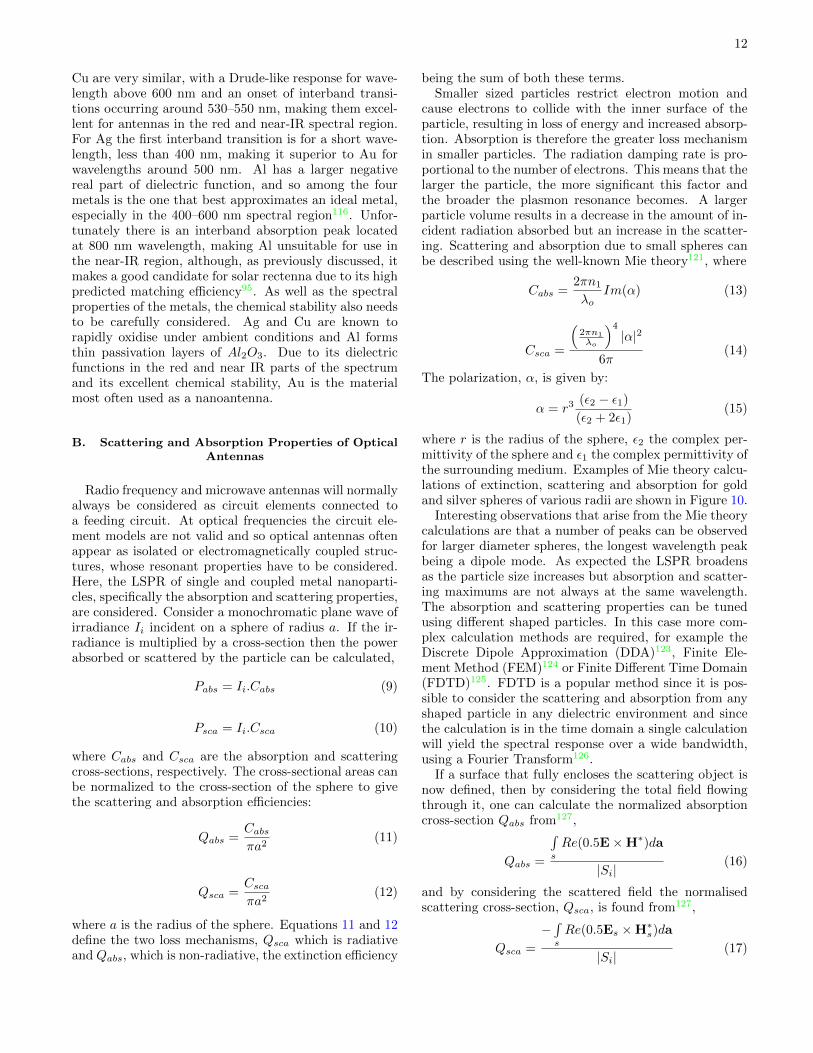
where r is the radius of the sphere, ε2 the complex per-mittivity of the sphere and ε1 the complex permittivity ofthe surrounding medium. Examples of Mie theory calcu-lations of extinction, scattering and absorption for goldand silver spheres of various radii are shown in Figure 10.
Interesting observations that arise from the Mie theorycalculations are that a number of peaks can be observedfor larger diameter spheres, the longest wavelength peakbeing a dipole mode. As expected the LSPR broadensas the particle size increases but absorption and scatter-ing maximums are not always at the same wavelength.The absorption and scattering properties can be tunedusing different shaped particles. In this case more com-plex calculation methods are required, for example theDiscrete Dipole Approximation (DDA)123, Finite Ele-ment Method (FEM)124 or Finite Different Time Domain(FDTD)125. FDTD is a popular method since it is pos-sible to consider the scattering and absorption from anyshaped particle in any dielectric environment and sincethe calculation is in the time domain a single calculationwill yield the spectral response over a wide bandwidth,using a Fourier Transform126.
If a surface that fully encloses the scattering object isnow defined, then by considering the total field flowingthrough it, one can calculate the normalized absorptioncross-section Qabs from127,
Qabs =
∫s
Re(0.5E×H∗)da
|Si|(16)
and by considering the scattered field the normalisedscattering cross-section, Qsca, is found from127,
Qsca =
−∫s
Re(0.5Es ×H∗s)da
|Si|(17)
13
FIG. 10. Mie calculations of extinction, scattering and absorption efficiencies for silver and gold nanospheres (a) Au sphere of20 nm radius (b) Ag sphere of 20 nm radius (c) Au sphere of 60 nm radius (d) Ag sphere of 60 nm radius (e) Au sphere of100 nm radius (f) Ag sphere of 100 nm radius.
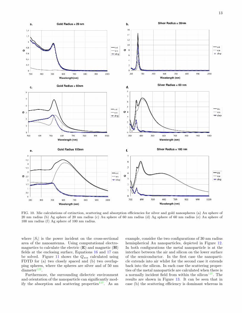
where |Si| is the power incident on the cross-sectionalarea of the nanoantenna. Using computational electro-magnetics to calculate the electric (E) and magnetic (H)fields at the enclosing surface, Equations 16 and 17 canbe solved. Figure 11 shows the Qsca calculated usingFDTD for (a) two closely spaced and (b) two overlap-ping spheres, where the spheres are silver and of 50 nmdiameter122.
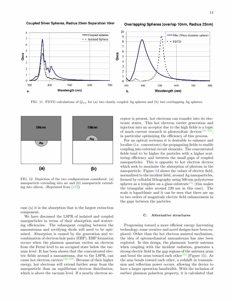
Furthermore, the surrounding dielectric environmentand orientation of the nanoparticle can significantly mod-ify the absorption and scattering properties127. As an
example, consider the two configurations of 30 nm radiushemispherical Au nanoparticles, depicted in Figure 12.In both configurations the metal nanoparticle is at theinterface between the air and silicon on the lower surfaceof the semiconductor. In the first case the nanoparti-cle extends into air whilst for the second case it extendsback into the silicon. In each case the scattering proper-ties of the metal nanoparticle are calculated when there isa normally incident field from within the silicon127. Theresults are shown in Figure 13. It can be seen that incase (b) the scattering efficiency is dominant whereas in
14
FIG. 11. FDTD calculations of Qsca for (a) two closely coupled Ag spheres and (b) two overlapping Ag spheres.
FIG. 12. Depiction of the two configurations considered: (a)nanoparticle extending into air and (b) nanoparticle extend-ing into silicon. (Reprinted from [127])
case (a) it is the absorption that is the largest extinctioncomponent.
We have discussed the LSPR of isolated and couplednanoparticles in terms of their absorption and scatter-ing efficiencies. The subsequent coupling between thenanoantenna and rectifying diode will need to be opti-mised. Absorption is caused by the generation and re-combination of electron hole pairs (EHP). EHP formationoccurs when the plasmon quantum excites an electronfrom the Fermi level to an occupied state below the vac-uum level. It has been shown that the concentrated elec-tric fields around a nanoantenna, due to the LSPR, cancause hot electron carriers128–130. Because of their higherenergy, hot electrons will extend further away from thenanoparticle than an equilibrium electron distribution,which is above the vacuum level. If a nearby electron ac-
ceptor is present, hot electrons can transfer into its elec-tronic states. This hot electron carrier generation andinjection into an acceptor due to the high fields is a topicof much current research in photovoltaic devices128–131,in particular optimizing the efficiency of this process.
For an optical rectenna it is desirable to enhance andlocalize (i.e. concentrate) the propagating fields to enablecoupling into external circuit elements. The concentratedfields tend to be higher for particles with a higher scat-tering efficiency and between the small gaps of couplednanoparticles. This is opposite to hot electron deviceswhich seek to maximise the absorption of photons in thenanoparticle. Figure 14 shows the values of electric field,normalized to the incident field, around Ag nanoparticles,formed by colloidal lithography using 500 nm polystyrenespheres as a template on a glass substrate132 (this makesthe triangular sides around 120 nm in this case). Thescale is logarithmic and it can be seen that there are upto two orders of magnitude electric field enhancement inthe gaps between the particles.
C. Alternative structures
Progressing toward a more efficient energy harvestingtechnology, some creative and novel designs have been ex-plored. Other than the hot electron assisted mechanism,the idea of optomechanical nanoantenna has also beenexplored. In this design, the plasmonic bowtie antennawhen coupling with the incident radiation, generates astrong electric field in the gap regions of the antenna armsand bend the arms toward each other133 (Figure 15). Asthe arm bends toward each other, a redshift in transmis-sion and reflection power occurs, allowing the device tohave a larger operation bandwidth. With the inclusion ofsurface plasmon polariton property, it is calculated that
15
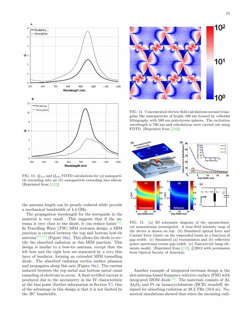
FIG. 13. Qsca and Qabs FDTD calculations for (a) nanoparti-cle extending into air (b) nanoparticle extending into silicon.(Reprinted from [127])
the antenna length can be greatly reduced while providea mechanical bandwidth of 4.4 GHz.
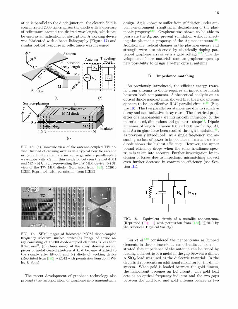
The propagation wavelength for the waveguide in thematerial is very small. This suggests that if the an-tenna is very close to the diode, it can reduce losses116.In Travelling Wave (TW) MIM rectenna design, a MIMjunction is created between the top and bottom bow-tieantenna134,178 (Figure 16a). This allows the diode to rec-tify the absorbed radiation at this MIM junction. Thisdesign is similar to a bow-tie antenna, except that theleft bow and the right bow are separated by a very thinlayer of insulator, forming an extended MIM tunnellingdiode. The absorbed radiation excites surface plasmonand propagates along this axis (Figure 16c). The currentinduced between the top metal and bottom metal causetunneling of electrons to occur. A final rectified current isproduced due to the asymmetry in the IV characteristicat the bias point (further information in Section V). Oneof the advantage in this design is that it is not limited bythe RC bandwidth.
FIG. 14. Concentrated electric field calculations around trian-gular like nanoparticles of height 100 nm formed by colloidallithography with 500 nm polystyrene spheres. The excitationwavelength is 780 nm and calculations were carried out usingFDTD. (Reprinted from [132])
FIG. 15. (a) 3D schematic diagram of the optomechani-cal nanoantenna investigated. A near-field intensity map ofthe device is shown on top. (b) Simulated optical force andCasimir force (inset) on the suspended beam as a function ofgap width. (c) Simulated (a) transmission and (b) reflectionpower spectrums versus gap width. (e) Nanocircuit lump ele-ments model. (Reprinted from [133], c©2012 with permissionfrom Optical Society of America)
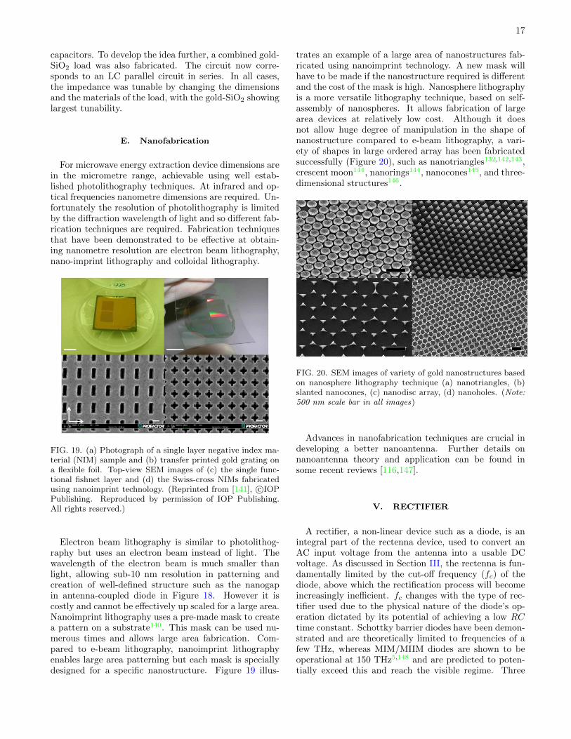
Another example of integrated rectenna design is theslot-antenna-based frequency selective surface (FSS) withintegrated MOM diode135. The materials consists of Al,Al2O3 and Pt on benzocyclobutene (BCB) standoff, de-signed for absorbing radiation at 28.3 THz (10.6 m). Nu-merical simulations showed that when the incoming radi-
16
ation is parallel to the diode junction, the electric field isconcentrated 2000 times across the diode with a decreaseof reflectance around the desired wavelength, which canbe used as an indication of absorption. A working devicewas fabricated with e-beam lithography (Figure 17) andsimilar optical response in reflectance was measured.
FIG. 16. (a) Isometric view of the antenna-coupled TW de-vice. Instead of crossing over as in a typical bow tie antennain figure 1, the antenna arms converge into a parallel-platewaveguide with a 2 nm thin insulator between the metal M1and M2. (b) Circuit representing the TW MIM device. (c) 3Dview of the TW MIM diode. (Reprinted from [134], c©2010IEEE. Reprinted, with permission, from IEEE)
FIG. 17. SEM images of fabricated MOM diode-coupledfrequency selective surface device.(a) Image of entire ar-ray consisting of 16,800 diode-coupled elements is less than0.325 mm2, (b) closer image of the array showing severalpieces of metal coated photoresist that became attached tothe sample after lift-off, and (c) diode of working device(Reprinted from [135], c©2012 with permission from John Wi-ley & Sons)
The recent development of graphene technology alsoprompts the incorporation of graphene into nanoantenna
design. Ag is known to suffer from sulfidation under am-bient environment, resulting in degradation of the plas-monic property136. Graphene was shown to be able topassivate the Ag and prevent sulfidation without affect-ing the plasmonic property of the Ag nanoantenna136.Additionally, radical changes in the plasmon energy andstrength were also observed by electrically doping pat-terned graphene arrays with a gate voltage137. The de-velopment of new materials such as graphene open upnew possibility to design a better optical antenna.
D. Impedance matching
As previously introduced, the efficient energy trans-fer from antenna to diode requires an impedance matchbetween both components. A theoretical analysis on anoptical dipole nanoantenna showed that the nanoantennaappears to be an effective RLC parallel circuit138 (Fig-ure 18). The two parallel resistances are due to radiativedecay and non-radiative decay rates. The electrical prop-erties of a nanoantenna are intrinsically influenced by thematerial used, dimensions and geometric shape95. Dipoleantennas of length between 100 and 350 nm for Ag, Al,and Au on glass have been studied through simulation95,as previously introduced. At a single frequency and as-suming no loss of power in impedance mismatch, a silverdipole shows the highest efficiency. However, the upperbound efficiency drops when the solar irradiance spec-trum is taken into account. Further investigation by in-clusion of losses due to impedance mismatching showedeven further decrease in conversion efficiency (see Sec-tion III).
FIG. 18. Equivalent circuit of a metallic nanoantenna.(Reprinted (Fig. 1) with permission from [138], c©2010 bythe American Physical Society)
Liu et al.139 considered the nanoantenna as lumpedelements in three-dimensional nanocircuits and demon-strated that impedance of the antenna can be tuned byloading a dielectric or a metal in the gap between a dimer.A SiO2 load was used as the dielectric material. In thecircuits it represents an additional capacitor for the dimersystem. When gold is loaded between the gold dimers,the nanocircuit becomes an LC circuit. The gold loadacts as an optical frequency inductor and the two gapsbetween the gold load and gold antenna behave as two
17
capacitors. To develop the idea further, a combined gold-SiO2 load was also fabricated. The circuit now corre-sponds to an LC parallel circuit in series. In all cases,the impedance was tunable by changing the dimensionsand the materials of the load, with the gold-SiO2 showinglargest tunability.
E. Nanofabrication
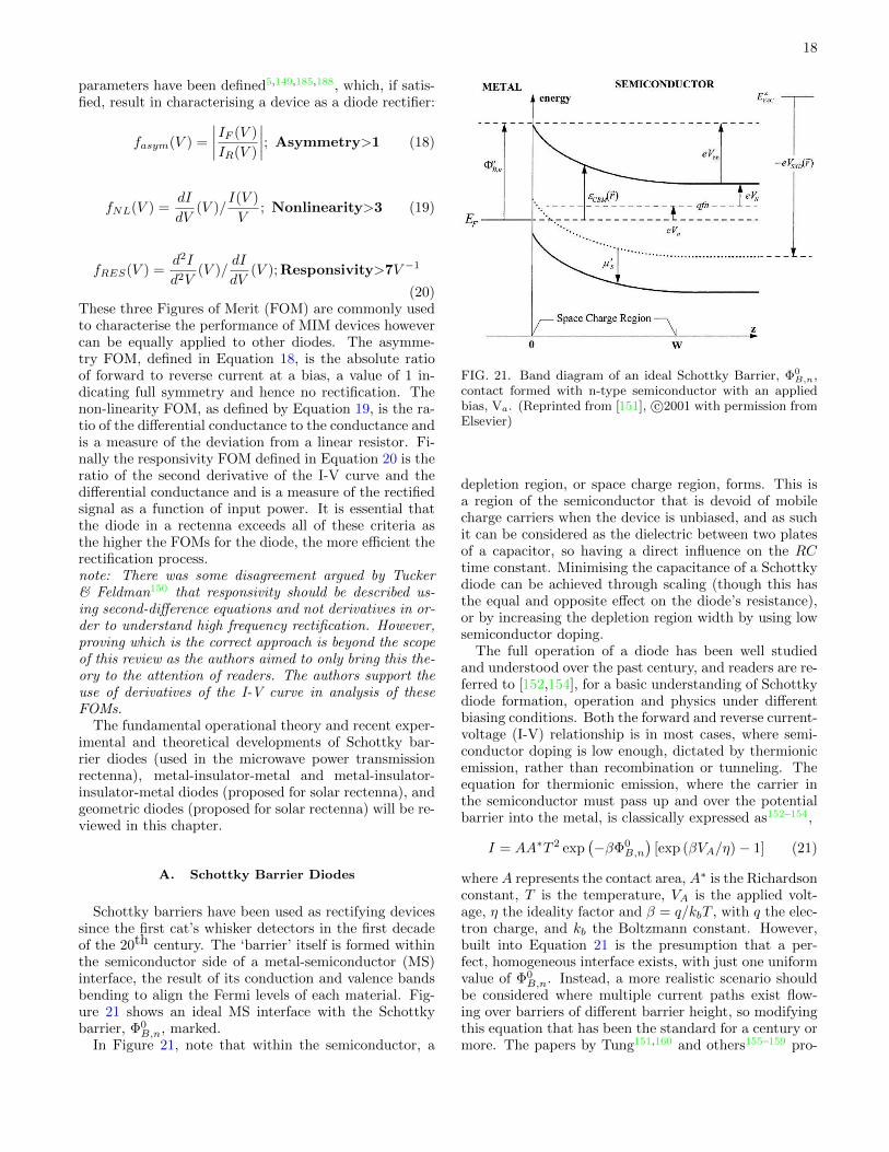
For microwave energy extraction device dimensions arein the micrometre range, achievable using well estab-lished photolithography techniques. At infrared and op-tical frequencies nanometre dimensions are required. Un-fortunately the resolution of photolithography is limitedby the diffraction wavelength of light and so different fab-rication techniques are required. Fabrication techniquesthat have been demonstrated to be effective at obtain-ing nanometre resolution are electron beam lithography,nano-imprint lithography and colloidal lithography.
FIG. 19. (a) Photograph of a single layer negative index ma-terial (NIM) sample and (b) transfer printed gold grating ona flexible foil. Top-view SEM images of (c) the single func-tional fishnet layer and (d) the Swiss-cross NIMs fabricatedusing nanoimprint technology. (Reprinted from [141], c©IOPPublishing. Reproduced by permission of IOP Publishing.All rights reserved.)
Electron beam lithography is similar to photolithog-raphy but uses an electron beam instead of light. Thewavelength of the electron beam is much smaller thanlight, allowing sub-10 nm resolution in patterning andcreation of well-defined structure such as the nanogapin antenna-coupled diode in Figure 18. However it iscostly and cannot be effectively up scaled for a large area.Nanoimprint lithography uses a pre-made mask to createa pattern on a substrate140. This mask can be used nu-merous times and allows large area fabrication. Com-pared to e-beam lithography, nanoimprint lithographyenables large area patterning but each mask is speciallydesigned for a specific nanostructure. Figure 19 illus-
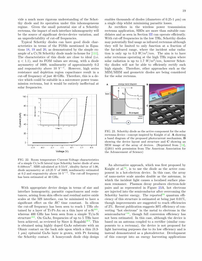
trates an example of a large area of nanostructures fab-ricated using nanoimprint technology. A new mask willhave to be made if the nanostructure required is differentand the cost of the mask is high. Nanosphere lithographyis a more versatile lithography technique, based on self-assembly of nanospheres. It allows fabrication of largearea devices at relatively low cost. Although it doesnot allow huge degree of manipulation in the shape ofnanostructure compared to e-beam lithography, a vari-ety of shapes in large ordered array has been fabricatedsuccessfully (Figure 20), such as nanotriangles132,142,143,crescent moon144, nanorings144, nanocones145, and three-dimensional structures146.
FIG. 20. SEM images of variety of gold nanostructures basedon nanosphere lithography technique (a) nanotriangles, (b)slanted nanocones, (c) nanodisc array, (d) nanoholes. (Note:500 nm scale bar in all images)
Advances in nanofabrication techniques are crucial indeveloping a better nanoantenna. Further details onnanoantenna theory and application can be found insome recent reviews [116,147].
V. RECTIFIER
A rectifier, a non-linear device such as a diode, is anintegral part of the rectenna device, used to convert anAC input voltage from the antenna into a usable DCvoltage. As discussed in Section III, the rectenna is fun-damentally limited by the cut-off frequency (fc) of thediode, above which the rectification process will becomeincreasingly inefficient. fc changes with the type of rec-tifier used due to the physical nature of the diode’s op-eration dictated by its potential of achieving a low RCtime constant. Schottky barrier diodes have been demon-strated and are theoretically limited to frequencies of afew THz, whereas MIM/MIIM diodes are shown to beoperational at 150 THz5,148 and are predicted to poten-tially exceed this and reach the visible regime. Three
18
parameters have been defined5,149,185,188, which, if satis-fied, result in characterising a device as a diode rectifier:
fasym(V ) =
∣∣∣∣IF (V )
IR(V )
∣∣∣∣; Asymmetry>1 (18)
fNL(V ) =dI
dV(V )/
I(V )
V; Nonlinearity>3 (19)
fRES(V ) =d2I
d2V(V )/
dI
dV(V );Responsivity>7V −1
(20)These three Figures of Merit (FOM) are commonly usedto characterise the performance of MIM devices howevercan be equally applied to other diodes. The asymme-try FOM, defined in Equation 18, is the absolute ratioof forward to reverse current at a bias, a value of 1 in-dicating full symmetry and hence no rectification. Thenon-linearity FOM, as defined by Equation 19, is the ra-tio of the differential conductance to the conductance andis a measure of the deviation from a linear resistor. Fi-nally the responsivity FOM defined in Equation 20 is theratio of the second derivative of the I-V curve and thedifferential conductance and is a measure of the rectifiedsignal as a function of input power. It is essential thatthe diode in a rectenna exceeds all of these criteria asthe higher the FOMs for the diode, the more efficient therectification process.note: There was some disagreement argued by Tucker& Feldman150 that responsivity should be described us-ing second-difference equations and not derivatives in or-der to understand high frequency rectification. However,proving which is the correct approach is beyond the scopeof this review as the authors aimed to only bring this the-ory to the attention of readers. The authors support theuse of derivatives of the I-V curve in analysis of theseFOMs.
The fundamental operational theory and recent exper-imental and theoretical developments of Schottky bar-rier diodes (used in the microwave power transmissionrectenna), metal-insulator-metal and metal-insulator-insulator-metal diodes (proposed for solar rectenna), andgeometric diodes (proposed for solar rectenna) will be re-viewed in this chapter.
A. Schottky Barrier Diodes
Schottky barriers have been used as rectifying devicessince the first cat’s whisker detectors in the first decadeof the 20th century. The ‘barrier’ itself is formed withinthe semiconductor side of a metal-semiconductor (MS)interface, the result of its conduction and valence bandsbending to align the Fermi levels of each material. Fig-ure 21 shows an ideal MS interface with the Schottkybarrier, Φ0
B,n, marked.In Figure 21, note that within the semiconductor, a
FIG. 21. Band diagram of an ideal Schottky Barrier, Φ0B,n,
contact formed with n-type semiconductor with an appliedbias, Va. (Reprinted from [151], c©2001 with permission fromElsevier)
depletion region, or space charge region, forms. This isa region of the semiconductor that is devoid of mobilecharge carriers when the device is unbiased, and as suchit can be considered as the dielectric between two platesof a capacitor, so having a direct influence on the RCtime constant. Minimising the capacitance of a Schottkydiode can be achieved through scaling (though this hasthe equal and opposite effect on the diode’s resistance),or by increasing the depletion region width by using lowsemiconductor doping.
The full operation of a diode has been well studiedand understood over the past century, and readers are re-ferred to [152,154], for a basic understanding of Schottkydiode formation, operation and physics under differentbiasing conditions. Both the forward and reverse current-voltage (I-V) relationship is in most cases, where semi-conductor doping is low enough, dictated by thermionicemission, rather than recombination or tunneling. Theequation for thermionic emission, where the carrier inthe semiconductor must pass up and over the potentialbarrier into the metal, is classically expressed as152–154,
I = AA∗T 2 exp(−βΦ0
B,n
)[exp (βVA/η)− 1] (21)
where A represents the contact area, A∗ is the Richardsonconstant, T is the temperature, VA is the applied volt-age, η the ideality factor and β = q/kbT , with q the elec-tron charge, and kb the Boltzmann constant. However,built into Equation 21 is the presumption that a per-fect, homogeneous interface exists, with just one uniformvalue of Φ0
B,n. Instead, a more realistic scenario shouldbe considered where multiple current paths exist flow-ing over barriers of different barrier height, so modifyingthis equation that has been the standard for a century ormore. The papers by Tung151,160 and others155–159 pro-
19
vide a much more rigorous understanding of the Schot-tky diode and its operation under this inhomogeneousregime. Given the small potential size of a Schottkyrectenna, the impact of such interface inhomogeneity willbe the source of significant device-device variation, andan unpredictability of cut-off frequencies.
Typical Schottky diodes can have good diode char-acteristics in terms of the FOMs mentioned in Equa-tions 18, 19 and 20, as demonstrated by the simple ex-ample of a Cr/Si Schottky diode made in-house for [155].The characteristics of this diode are close to ideal (i.e.η < 1.1), and its FOM values are strong, with a diodeasymmetry of 1669, nonlinearity of approximately 0.2and responsivity above 10 V −1. However, high seriesresistance and depletion region capacitance result in acut-off frequency of just 40 GHz. Therefore, this is a de-vice which could be suitable in a microwave power trans-mission rectenna, but it would be entirely ineffectual atsolar frequencies.
FIG. 22. Room temperature Current-Voltage characteristicsof a simple Cr/n-Si lateral type Schottky barier diode of area0.448mm3. SBH calculated at 0.51eV , ideality factor of 1.06,diode asymmetry at ±0.25 V of 1669, nonlinearity estimatedat 0.2 and responsivity above 10 V −1. The cut-off frequencyhas been estimated at 40 GHz.
With appropriate device design in terms of size andinterface homogeneity, parasitic capacitances and resis-tances, arising from skin effects and residual native oxidescales at the MS interface, can be minimised to have asignificant effect on the RC time constant. In siliconthe cut-off frequency has been seen to reach 1 THz ob-tained by a layer of Ti-Pt-Au on a thin layer of n-Si161,whereas 400 GHz has been seen from a simple Ti/n-Sistructure162. On GaAs, frequencies of up to 5 THz havebeen achieved, as reviewed by Sizov & Rogalski163. Thisis obtained using highly doped GaAs substrate with anOhmic contact on the back side upon which a thin (0.3-1 µm) epitaxial GaAs layer is grown, with Pt formingthe Schottky contact. A honeycomb diode chip design
enables thousands of diodes (diameters of 0.25-1 µm) ona single chip whilst minimising parasitic losses.
As rectifiers in the wireless power transmissionrectenna application, SBDs are more than suitable can-didates and as seen in Section III can operate efficiently.With cut-off frequencies in the low THz, Schottky diodesmay potentially find usage as infrared rectennas althoughthey will be limited to only function at a fraction ofthe far-infrared range, where the incident solar radia-tion is only up to 0.3 W/m2/nm. The aim is to havesolar rectennas operating at the high THz region wheresolar radiation is up to 1.7 W/m2/nm, however Schot-tky diodes will not be able to efficiently rectify suchhigh signals. Therefore, other approaches such as theMIM/MIIM and geometric diodes are being consideredfor the solar rectenna.
FIG. 23. Schottky diode as the active component for the solarrectenna device - concept inspired by Knight et al. A showinga band diagram of the proposed photocurrent mechanism, Bshowing the device layout and structure and C showing anSEM image of the array of devices. (Reprinted from [94],c©2011 with permission from The American Association for
the Advancement of Science)
An alternative approach, which was first proposed byKnight et al.94, is to use the diode as the active com-ponent in a hot-electron device. In this case, the arrayof nano-metre scale anodes double as the antennas, inwhich the incident light causes a localised surface plas-mon resonance. Plasmon decay produces electron-holepairs and as represented in Figure 23A, hot electronsare injected into the semiconductor after overcoming theSchottky barrier energy. The reported94 quantum effi-ciency of this structure is estimated at being just 0.01%,though improvements are suggested to reach efficienciesof 2%. Recent publication suggests 30% efficiency of con-verting “hot electrons” in the metal to electrons in thesemiconductor164, though full conversion efficiency hasnot been estimated. In this case, although the device isbased on an antenna coupled to a rectifier (similar com-ponents to a rectenna), the device is not proposed forlight harvesting purposes due to its low efficiency and isinstead demonstrated as a photodetector. Developmentof this concept into an energy harvesting applications
20
would require the conversion efficiency to be increased,though with the current state-of-art, this seems improb-able.
B. Metal-Insulator-Metal Diodes
Current transport in Metal-Insulator-Metal (MIM)diodes is due to quantum electron tunnelling through anultra-thin insulator layer (typically < 10 nm165). Recti-fication in these devices is due to variation in tunnellingrates caused by barrier asymmetry due to material selec-tion, device geometry, thermal asymmetry, and photoninduced deviation in electron flux distribution across oc-cupied and unoccupied states105, all contributing towardsa nonlinear asymmetric I-V response. In the current re-view, we will qualitatively explain the nature of the I-Vasymmetry taking into account the material selection forplanar MIM devices under no illumination and thermalequilibrium. Under illumination, electron tunnelling isstimulated by different processes depending whether anantenna is or is not coupled to the diode. Further readingis suggested in [105,165,166,169]. Thermionic emissionalso contributes to tunnel diodes’ I-V curves165,188,189,especially to devices with thick insulating layers188.
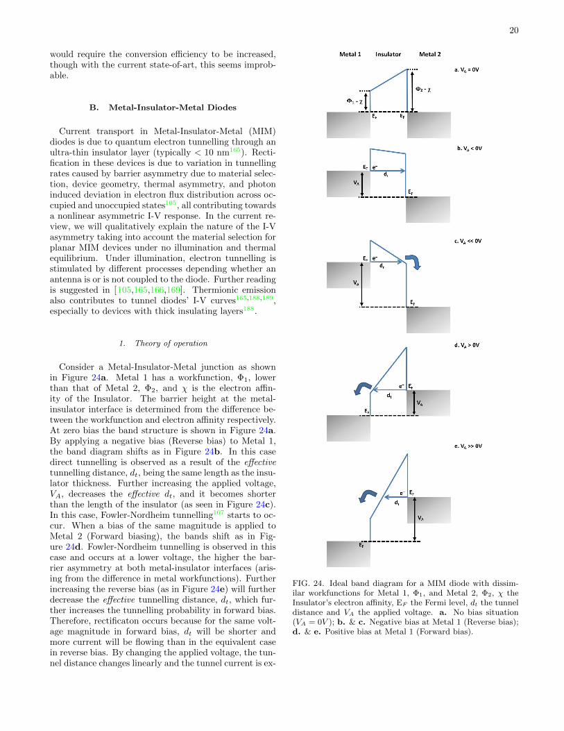
1. Theory of operation
Consider a Metal-Insulator-Metal junction as shownin Figure 24a. Metal 1 has a workfunction, Φ1, lowerthan that of Metal 2, Φ2, and χ is the electron affin-ity of the Insulator. The barrier height at the metal-insulator interface is determined from the difference be-tween the workfunction and electron affinity respectively.At zero bias the band structure is shown in Figure 24a.By applying a negative bias (Reverse bias) to Metal 1,the band diagram shifts as in Figure 24b. In this casedirect tunnelling is observed as a result of the effectivetunnelling distance, dt, being the same length as the insu-lator thickness. Further increasing the applied voltage,VA, decreases the effective dt, and it becomes shorterthan the length of the insulator (as seen in Figure 24c).In this case, Fowler-Nordheim tunnelling167 starts to oc-cur. When a bias of the same magnitude is applied toMetal 2 (Forward biasing), the bands shift as in Fig-ure 24d. Fowler-Nordheim tunnelling is observed in thiscase and occurs at a lower voltage, the higher the bar-rier asymmetry at both metal-insulator interfaces (aris-ing from the difference in metal workfunctions). Furtherincreasing the reverse bias (as in Figure 24e) will furtherdecrease the effective tunnelling distance, dt, which fur-ther increases the tunnelling probability in forward bias.Therefore, rectificaton occurs because for the same volt-age magnitude in forward bias, dt will be shorter andmore current will be flowing than in the equivalent casein reverse bias. By changing the applied voltage, the tun-nel distance changes linearly and the tunnel current is ex-
FIG. 24. Ideal band diagram for a MIM diode with dissim-ilar workfunctions for Metal 1, Φ1, and Metal 2, Φ2, χ theInsulator’s electron affinity, EF the Fermi level, dt the tunneldistance and VA the applied voltage. a. No bias situation(VA = 0V ); b. & c. Negative bias at Metal 1 (Reverse bias);d. & e. Positive bias at Metal 1 (Forward bias).
21
ponentially dependant on this distance168. This leads toan asymmetric, nonlinear current-voltage response and isthe origin of the rectification mechanism in MIM diodes.
2. Experimental devices
Various metal-insulator systems have been used to in-vestigate the rectification behaviour of MIM diodes. Re-search attempts are concentrated either towards mod-elling the behaviour and rectification properties or im-proving the figure of merits by optimising the material se-lection and fabrication techniques of these structures. Astheory suggests, using similar metals in the MIM configu-ration should yield symmetric I-V curves, however asym-metric I-V curves have been reported for Al/Al2O3/Al170
with structures and experiments conducted by the au-thors on Ti/TiO2/Ti and Nb/Nb2O5/Nb devices havingalso displayed asymmetric I-V curves for these structures.The origin of this asymmetry is suspected to come fromthe formation of two different metal-insulator interfacesarising from dissimilar deposition processes, thus creat-ing regions of enhanced leakage currents through the bar-rier. Other reported structures with optimised oxide lay-ers such as Ni/NiO/Ni108,174,176–178,180, Al/Al2O3/Al171
and Nb/Nb2O5/Nb149,185,187 show symmetry in the I-Vcurves, which is compliant with theoretical predictions.Although not displaying rectification properties, theNi/NiO/Ni system is widely used for detection and mix-ing up to 30 THz infrared radiation due its significantlylow resistance-area product of 1 Ω(µm2)108,176–178, whichindicates the potential for a low RC constant. Howeverdue to a lack of asymmetry, the second Ni electrode mustbe replaced with a metal of different workfunction in or-der to achieve rectification. This has been investigatedby Hoofring et al.175, Krishnan et al.111,179 and Esfandi-ari et al.181 with Au, Cr and Pt contacts respectively, alldisplaying good asymmetrical I-V response. Other struc-tures of dissimilar materials which have shown promis-ing results are Al/Al2O3/Ni172, Nb/Nb2O5/Pt149,184,185,ZrCuAlNi/Al2O3/Al182 and also Nb/Nb2O5/Ag (testedin-house and by [190]). More tested metal-insulator com-binations are listed in [149].
ZrCuAlNi was suggested as an electrode due to itslow roughness after growth, making it suitable for MIMdevices182,183. However, it is not ideal due to formationof an interfacial compound at the interface with the in-sulator. This was highlighted by Grover & Moddel168,who anticipated the importance of material selectionfor a good MIM and that arbitrary combinations ofmetals and oxides are not always feasible, as for ex-ample Al/Al2O3/Pt173 displays a linear I-V and yethas been successfully shown to work in an antenna-coupled infrared detector. A study by Heiblum et al.174
tested Al/Al2O3/Al, Cr/Cr2O3/Au, Al/Al2O3/Ag andNb/Nb2O5/Au MIMs by exposing them to an IR laserand concluded their poor rectification properties due tothe production of large thermal contributions when ex-
posed to laser radiation. This is a very useful approach,which must be applied to other MIM candidates for so-lar applications. An alternative concept was previouslydescribed (Figure 16), consisting of a MIM diode basedon a travelling-wave structure, which although havinga symmetrical configuration (Nb/Nb2O5/Nb), outper-forms planar type MIM diodes by three orders of magni-tude at µm wavelength134.
One of the most important findings in this field isa method for characterising the electrical properties ofMIM devices by nanoindentation and later a bent wiretechnique suggested by Periasamy et al.149,184–187. Theconcept is based on a metal being deposited on a sili-con substrate, after which a continuous oxide is grownand the second electrode is a bent wire of a desired ma-terial. This ensures a small contact area and the abil-ity to characterise a point-contact type MIM junction.This work is very useful as it gives the chance to studyvarious metal-insulator combinations before attemptingto optimise planar thin-film diode devices. This tech-nique was used to systematically study the influence themetal workfunction difference has on the electrical prop-erties of MIM diodes (reference [149]). The structuresanalysed have a Nb bottom electrode, Nb2O5 insulatorgrown by anodic oxidation, and eight different metal 2selections (Hf, Zr, Nb, Ti, Cu, Ag, Au, and Pt). Theresult was that the workfunction difference has a directinfluence on rectification properties, with the asymmetryincreasing sharply for ∆Φ > kBT . This agrees with the-oretical predictions and with the models by Simmons191.Conversely, nonlinearity FOM displayed no direct cor-relation with ∆Φ. The highest FOMs were observedfor Nb/Nb2O5/Pt, which displayed 1500 asymmetry, 4nonlinearity and 20 V −1 responsivity meeting the cri-teria outlined in Equations 18, 19 and 20. Recently,this work was continued through (reference [ 188]) thefabrication of 6400µm2 planar devices with the sameNb/Nb2O5 base and six metal top contacts (Ag, Cu,Nb, Ni, Au and Pt). The work confirmed a direct lin-ear relation between increasing asymmetry and increas-ing ∆Φ with Nb/Nb2O5/Pt showing optimal results withfigure of merits of 7742 asymmetry, 4.7 nonlineary and52.2 V −1 responsivity. These are to our knowledge thelargest FOM values recorded and hence the most promis-ing structure to be successfully integrated into a solarrectenna.
Periasamy et al.185 also characterise other oxides witha Nb metal base and Pt bent wire and prove a hypothe-sis whereby the best rectification properties are expectedfrom using dissimilar metals and low barrier heights ateach metal-insulator interface in order to sooner promotethe faster Fowler-Nordheim tunnelling in the forward di-rection. To achieve smaller barriers, high electron affinityinsulators must be selected. Due to this reason, Nb2O5
and TiO2 outperform Al2O3 and MgO. Another require-ment for the insulator is a large dielectric constant sincefor small area devices the capacitance is reduced, how-ever due to the requirements for tunneling the ultra-thin
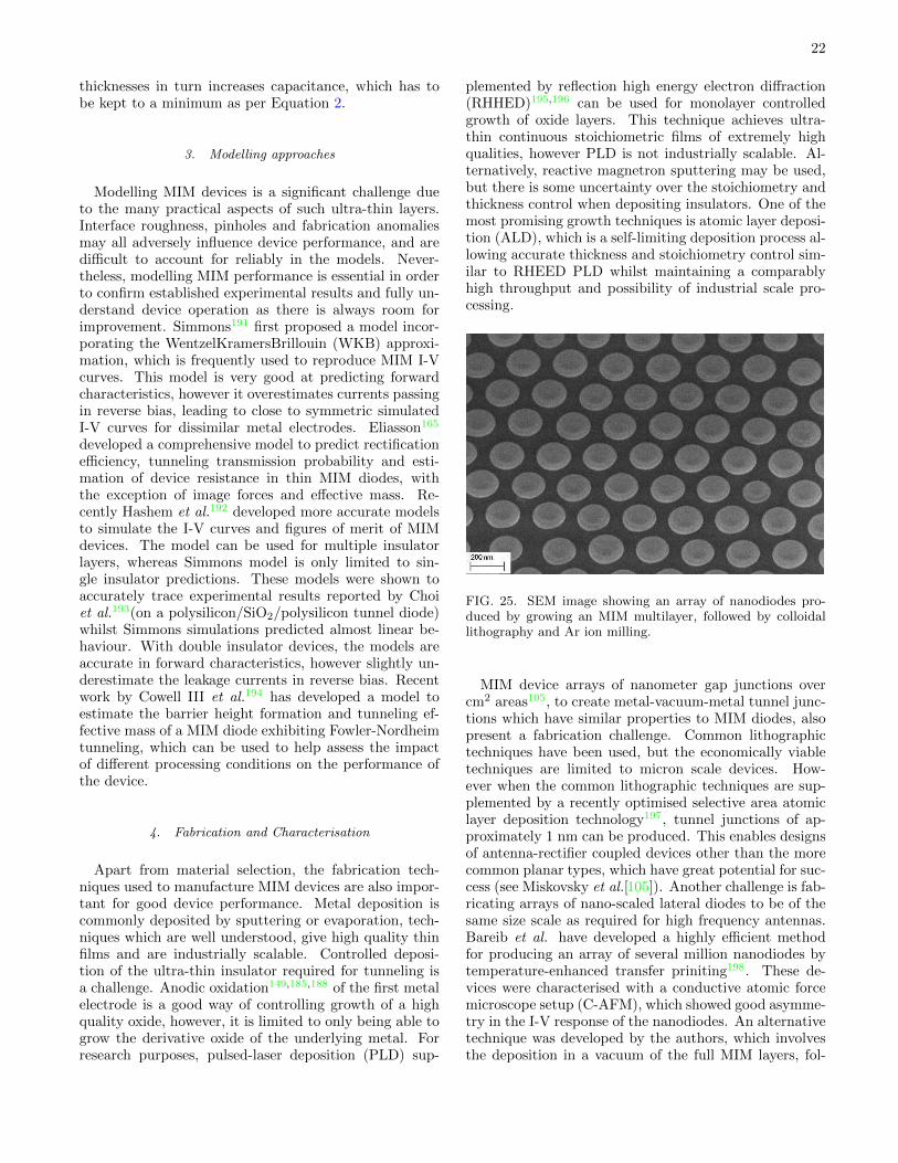
22
thicknesses in turn increases capacitance, which has tobe kept to a minimum as per Equation 2.
3. Modelling approaches
Modelling MIM devices is a significant challenge dueto the many practical aspects of such ultra-thin layers.Interface roughness, pinholes and fabrication anomaliesmay all adversely influence device performance, and aredifficult to account for reliably in the models. Never-theless, modelling MIM performance is essential in orderto confirm established experimental results and fully un-derstand device operation as there is always room forimprovement. Simmons191 first proposed a model incor-porating the WentzelKramersBrillouin (WKB) approxi-mation, which is frequently used to reproduce MIM I-Vcurves. This model is very good at predicting forwardcharacteristics, however it overestimates currents passingin reverse bias, leading to close to symmetric simulatedI-V curves for dissimilar metal electrodes. Eliasson165
developed a comprehensive model to predict rectificationefficiency, tunneling transmission probability and esti-mation of device resistance in thin MIM diodes, withthe exception of image forces and effective mass. Re-cently Hashem et al.192 developed more accurate modelsto simulate the I-V curves and figures of merit of MIMdevices. The model can be used for multiple insulatorlayers, whereas Simmons model is only limited to sin-gle insulator predictions. These models were shown toaccurately trace experimental results reported by Choiet al.193(on a polysilicon/SiO2/polysilicon tunnel diode)whilst Simmons simulations predicted almost linear be-haviour. With double insulator devices, the models areaccurate in forward characteristics, however slightly un-derestimate the leakage currents in reverse bias. Recentwork by Cowell III et al.194 has developed a model toestimate the barrier height formation and tunneling ef-fective mass of a MIM diode exhibiting Fowler-Nordheimtunneling, which can be used to help assess the impactof different processing conditions on the performance ofthe device.
4. Fabrication and Characterisation
Apart from material selection, the fabrication tech-niques used to manufacture MIM devices are also impor-tant for good device performance. Metal deposition iscommonly deposited by sputtering or evaporation, tech-niques which are well understood, give high quality thinfilms and are industrially scalable. Controlled deposi-tion of the ultra-thin insulator required for tunneling isa challenge. Anodic oxidation149,185,188 of the first metalelectrode is a good way of controlling growth of a highquality oxide, however, it is limited to only being able togrow the derivative oxide of the underlying metal. Forresearch purposes, pulsed-laser deposition (PLD) sup-
plemented by reflection high energy electron diffraction(RHHED)195,196 can be used for monolayer controlledgrowth of oxide layers. This technique achieves ultra-thin continuous stoichiometric films of extremely highqualities, however PLD is not industrially scalable. Al-ternatively, reactive magnetron sputtering may be used,but there is some uncertainty over the stoichiometry andthickness control when depositing insulators. One of themost promising growth techniques is atomic layer deposi-tion (ALD), which is a self-limiting deposition process al-lowing accurate thickness and stoichiometry control sim-ilar to RHEED PLD whilst maintaining a comparablyhigh throughput and possibility of industrial scale pro-cessing.
FIG. 25. SEM image showing an array of nanodiodes pro-duced by growing an MIM multilayer, followed by colloidallithography and Ar ion milling.
MIM device arrays of nanometer gap junctions overcm2 areas105, to create metal-vacuum-metal tunnel junc-tions which have similar properties to MIM diodes, alsopresent a fabrication challenge. Common lithographictechniques have been used, but the economically viabletechniques are limited to micron scale devices. How-ever when the common lithographic techniques are sup-plemented by a recently optimised selective area atomiclayer deposition technology197, tunnel junctions of ap-proximately 1 nm can be produced. This enables designsof antenna-rectifier coupled devices other than the morecommon planar types, which have great potential for suc-cess (see Miskovsky et al.[105]). Another challenge is fab-ricating arrays of nano-scaled lateral diodes to be of thesame size scale as required for high frequency antennas.Bareib et al. have developed a highly efficient methodfor producing an array of several million nanodiodes bytemperature-enhanced transfer priniting198. These de-vices were characterised with a conductive atomic forcemicroscope setup (C-AFM), which showed good asymme-try in the I-V response of the nanodiodes. An alternativetechnique was developed by the authors, which involvesthe deposition in a vacuum of the full MIM layers, fol-
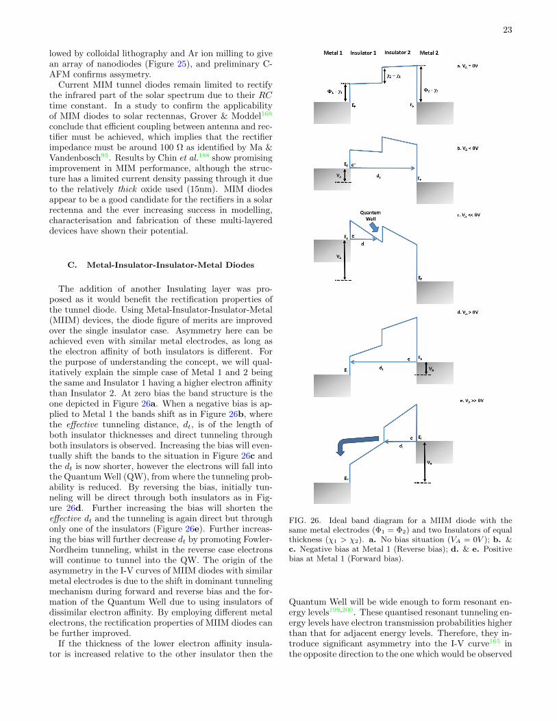
23
lowed by colloidal lithography and Ar ion milling to givean array of nanodiodes (Figure 25), and preliminary C-AFM confirms assymetry.
Current MIM tunnel diodes remain limited to rectifythe infrared part of the solar spectrum due to their RCtime constant. In a study to confirm the applicabilityof MIM diodes to solar rectennas, Grover & Moddel168
conclude that efficient coupling between antenna and rec-tifier must be achieved, which implies that the rectifierimpedance must be around 100 Ω as identified by Ma &Vandenbosch95. Results by Chin et al.188 show promisingimprovement in MIM performance, although the struc-ture has a limited current density passing through it dueto the relatively thick oxide used (15nm). MIM diodesappear to be a good candidate for the rectifiers in a solarrectenna and the ever increasing success in modelling,characterisation and fabrication of these multi-layereddevices have shown their potential.
C. Metal-Insulator-Insulator-Metal Diodes
The addition of another Insulating layer was pro-posed as it would benefit the rectification properties ofthe tunnel diode. Using Metal-Insulator-Insulator-Metal(MIIM) devices, the diode figure of merits are improvedover the single insulator case. Asymmetry here can beachieved even with similar metal electrodes, as long asthe electron affinity of both insulators is different. Forthe purpose of understanding the concept, we will qual-itatively explain the simple case of Metal 1 and 2 beingthe same and Insulator 1 having a higher electron affinitythan Insulator 2. At zero bias the band structure is theone depicted in Figure 26a. When a negative bias is ap-plied to Metal 1 the bands shift as in Figure 26b, wherethe effective tunneling distance, dt, is of the length ofboth insulator thicknesses and direct tunneling throughboth insulators is observed. Increasing the bias will even-tually shift the bands to the situation in Figure 26c andthe dt is now shorter, however the electrons will fall intothe Quantum Well (QW), from where the tunneling prob-ability is reduced. By reversing the bias, initially tun-neling will be direct through both insulators as in Fig-ure 26d. Further increasing the bias will shorten theeffective dt and the tunneling is again direct but throughonly one of the insulators (Figure 26e). Further increas-ing the bias will further decrease dt by promoting Fowler-Nordheim tunneling, whilst in the reverse case electronswill continue to tunnel into the QW. The origin of theasymmetry in the I-V curves of MIIM diodes with similarmetal electrodes is due to the shift in dominant tunnelingmechanism during forward and reverse bias and the for-mation of the Quantum Well due to using insulators ofdissimilar electron affinity. By employing different metalelectrons, the rectification properties of MIIM diodes canbe further improved.
If the thickness of the lower electron affinity insula-tor is increased relative to the other insulator then the
FIG. 26. Ideal band diagram for a MIIM diode with thesame metal electrodes (Φ1 = Φ2) and two Insulators of equalthickness (χ1 > χ2). a. No bias situation (VA = 0V ); b. &c. Negative bias at Metal 1 (Reverse bias); d. & e. Positivebias at Metal 1 (Forward bias).
Quantum Well will be wide enough to form resonant en-ergy levels199,200. These quantised resonant tunneling en-ergy levels have electron transmission probabilities higherthan that for adjacent energy levels. Therefore, they in-troduce significant asymmetry into the I-V curve165 inthe opposite direction to the one which would be observed
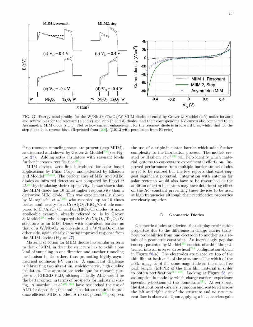
24
FIG. 27. Energy-band profiles for the W/Nb2O5/Ta2O5/W MIIM diodes discused by Grover & Moddel (left) under forwardand reverse bias for the resonant (a and c) and step (b and d) diodes, and their corresponding I-V curves also compared to anAsymmetric MIM diode (right). Notice how current enhancement for the resonant diode is in forward bias, whilst that for thestep diode is in reverse bias. (Reprinted from [200], c©2012 with permission from Elsevier)
if no resonant tunneling states are present (step MIIM),as discussed and shown by Grover & Moddel200(see Fig-ure 27). Adding extra insulators with resonant levelsfurther increases rectification201.
MIIM devices were first introduced for solar basedapplications by Phiar Corp. and patented by Eliassonand Moddel202,203. The performance of MIM and MIIMdiodes as infra-red detectors was compared by Hegyi etal.204 by simulating their responsivity. It was shown thatthe MIIM diode has 10 times higher responsivity than aderivative MIM diode. This was experimentally shownby Maraghechi et al.205 who recorded up to 10 timesbetter nonlinearity for a Cr/Al2O3/HfO2/Cr diode com-pared to Cr/Al2O3/Cr and Cr/HfO2/Cr diodes. A moreapplicable example, already referred to, is by Grover& Moddel200, who compared their W/Nb2O5/Ta2O5/Wstructure to an MIM Diode with equivalent barriers asthat of a W/Nb2O5 on one side and a W/Ta2O5 on theother side, again clearly showing improved response fromthe MIIM device (Figure 27).
Material selection for MIIM diodes has similar criteriato that of MIM, in that the structure has to exhibit onekind of tunneling in one direction and another tunnelingmechanism in the other, thus promoting highly asym-metrical nonlinear I-V curves. A significant challengeis fabricating two ultra-thin, stoichiometric, high qualityinsulators. The appropriate technique for research pur-poses is RHEED PLD, although ideally ALD would bethe better option in terms of prospects for industrial scal-ing. Alimardani et al.206–208 have researched the use ofALD for depositing the double insulators required to pro-duce efficient MIIM diodes. A recent patent209 proposes
the use of a triple-insulator barrier which adds furthercomplexity to the fabrication process. The models cre-ated by Hashem et al.192 will help identify which mate-rial systems to concentrate experimental efforts on. Im-proved performance from multiple barrier tunnel diodesis yet to be realised but the few reports that exist sug-gest significant potential. Integration with antenna forsolar rectenna would also have to be researched as theaddition of extra insulators may have deteriorating effecton the RC constant preventing these devices to be usedat high frequencies although their rectification propertiesare clearly superior.
D. Geometric Diodes
Geometric diodes are devices that display rectificationproperties due to the difference in charge carrier trans-port probabilities from one electrode to another as a re-sult of a geometric constraint. An increasingly popularconcept patented by Moddel210 consists of a thin film pat-terned into an inverse arrowhead214 configuration shownin Figure 28(a). The electrodes are placed on top of thethin film at both ends of the structure. The width of theneck, dneck, is of the same magnitude as the mean-freepath length (MFPL) of the thin film material in orderto obtain rectification211–215. Looking at Figure 28, anassumption is made by which charge carriers experiencespecular reflections at the boundaries211. At zero bias,the distribution of carriers is random and scattered acrossthe left and right side of the structure and no net cur-rent flow is observed. Upon applying a bias, carriers gain
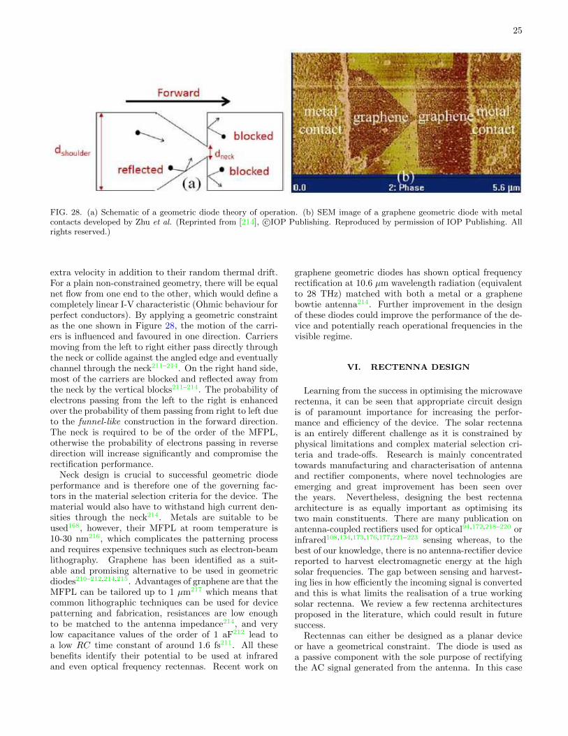
25
FIG. 28. (a) Schematic of a geometric diode theory of operation. (b) SEM image of a graphene geometric diode with metalcontacts developed by Zhu et al. (Reprinted from [214], c©IOP Publishing. Reproduced by permission of IOP Publishing. Allrights reserved.)
extra velocity in addition to their random thermal drift.For a plain non-constrained geometry, there will be equalnet flow from one end to the other, which would define acompletely linear I-V characteristic (Ohmic behaviour forperfect conductors). By applying a geometric constraintas the one shown in Figure 28, the motion of the carri-ers is influenced and favoured in one direction. Carriersmoving from the left to right either pass directly throughthe neck or collide against the angled edge and eventuallychannel through the neck211–214. On the right hand side,most of the carriers are blocked and reflected away fromthe neck by the vertical blocks211–214. The probability ofelectrons passing from the left to the right is enhancedover the probability of them passing from right to left dueto the funnel-like construction in the forward direction.The neck is required to be of the order of the MFPL,otherwise the probability of electrons passing in reversedirection will increase significantly and compromise therectification performance.
Neck design is crucial to successful geometric diodeperformance and is therefore one of the governing fac-tors in the material selection criteria for the device. Thematerial would also have to withstand high current den-sities through the neck214. Metals are suitable to beused168, however, their MFPL at room temperature is10-30 nm216, which complicates the patterning processand requires expensive techniques such as electron-beamlithography. Graphene has been identified as a suit-able and promising alternative to be used in geometricdiodes210–212,214,215. Advantages of graphene are that theMFPL can be tailored up to 1 µm217 which means thatcommon lithographic techniques can be used for devicepatterning and fabrication, resistances are low enoughto be matched to the antenna impedance214, and verylow capacitance values of the order of 1 aF212 lead toa low RC time constant of around 1.6 fs211. All thesebenefits identify their potential to be used at infraredand even optical frequency rectennas. Recent work on
graphene geometric diodes has shown optical frequencyrectification at 10.6 µm wavelength radiation (equivalentto 28 THz) matched with both a metal or a graphenebowtie antenna214. Further improvement in the designof these diodes could improve the performance of the de-vice and potentially reach operational frequencies in thevisible regime.
VI. RECTENNA DESIGN
Learning from the success in optimising the microwaverectenna, it can be seen that appropriate circuit designis of paramount importance for increasing the perfor-mance and efficiency of the device. The solar rectennais an entirely different challenge as it is constrained byphysical limitations and complex material selection cri-teria and trade-offs. Research is mainly concentratedtowards manufacturing and characterisation of antennaand rectifier components, where novel technologies areemerging and great improvement has been seen overthe years. Nevertheless, designing the best rectennaarchitecture is as equally important as optimising itstwo main constituents. There are many publication onantenna-coupled rectifiers used for optical94,172,218–220 orinfrared108,134,173,176,177,221–223 sensing whereas, to thebest of our knowledge, there is no antenna-rectifier devicereported to harvest electromagnetic energy at the highsolar frequencies. The gap between sensing and harvest-ing lies in how efficiently the incoming signal is convertedand this is what limits the realisation of a true workingsolar rectenna. We review a few rectenna architecturesproposed in the literature, which could result in futuresuccess.
Rectennas can either be designed as a planar deviceor have a geometrical constraint. The diode is used asa passive component with the sole purpose of rectifyingthe AC signal generated from the antenna. In this case
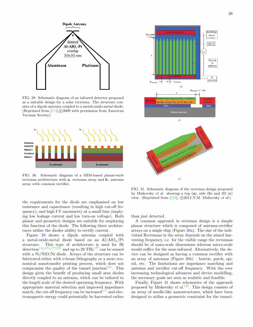
26
FIG. 29. Schematic diagram of an infrared detector proposedas a suitable design for a solar rectenna. The structure con-sists of a dipole antenna coupled to a metal-oxide-metal diode.(Reprinted from [173], c©2009 with permission from AmericanVacuum Society)
FIG. 30. Schematic diagram of a MIM-based planar-stylerectenna architecture with a. rectenna array and b. antennaarray with common rectifier.
the requirements for the diode are emphasised on lowresistance and capacitance (resulting in high cut-off fre-quency), and high I-V asymmetry at a small bias (imply-ing low leakage current and low turn-on voltage). Bothplanar and geometric designs are suitable for employingthis function of the diode. The following three architec-tures utilise the diodes ability to rectify current.
Figure 29 shows a dipole antenna coupled witha metal-oxide-metal diode based on an Al/AlOx/Ptstructure. This type of architecture is used for IRdetection134,173,177,221 and up to 28 THz177 can be sensedwith a Ni/NiO/Ni diode. Arrays of the structure can befabricated either with e-beam lithography or a more eco-nomical nanotransfer printing process, which does notcompromise the quality of the tunnel junction221. Thisdesign gives the benefit of producing small area diodesdirectly coupled to an antenna, which can be tailored tothe length scale of the desired operating frequency. Withappropriate material selection and improved impedancematch, the cut-off frequency can be increased177 and elec-tromagnetic energy could potentially be harvested rather
FIG. 31. Schematic diagram of the rectenna design proposedby Miskovsky et al. showing a top (a), side (b) and 3D (c)view. (Reprinted from [105], c©2012 N.M. Miskovsky et al.)
than just detected.A common approach in rectenna design is a simple
planar structure which is composed of antenna-rectifierarrays on a single chip (Figure 30a). The size of the indi-vidual Rectennas in the array depends on the aimed har-vesting frequency, i.e. for the visible range the rectennasshould be of nano-scale dimensions whereas micro-scalewould suffice for the near-infrared. Alternatively, the de-vice can be designed as having a common rectifier withan array of antennas (Figure 30b) – bowtie, patch, spi-ral, etc. The limitations are impedance matching andantenna and rectifier cut-off frequency. With the everincreasing technological advances and device modelling,the necessary goals are seen as realistic and feasible.
Finally, Figure 31 shows schematics of the approachproposed by Miskovsky et al.105. This design consists ofan array of needle-like nanostructures, which have beendesigned to utilise a geometric constraint for the tunnel-
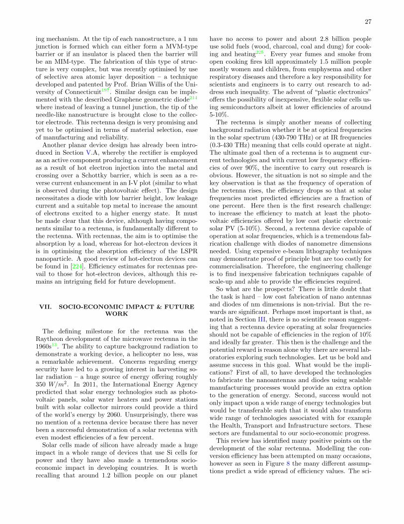
27
ing mechanism. At the tip of each nanostructure, a 1 nmjunction is formed which can either form a MVM-typebarrier or if an insulator is placed then the barrier willbe an MIM-type. The fabrication of this type of struc-ture is very complex, but was recently optimised by useof selective area atomic layer deposition – a techniquedeveloped and patented by Prof. Brian Willis of the Uni-versity of Connecticuit197. Similar design can be imple-mented with the described Graphene geometric diode214
where instead of leaving a tunnel junction, the tip of theneedle-like nanostructure is brought close to the collec-tor electrode. This rectenna design is very promising andyet to be optimised in terms of material selection, easeof manufacturing and reliability.
Another planar device design has already been intro-duced in Section V.A, whereby the rectifier is employedas an active component producing a current enhancementas a result of hot electron injection into the metal andcrossing over a Schottky barrier, which is seen as a re-verse current enhancement in an I-V plot (similar to whatis observed during the photovoltaic effect). The designnecessitates a diode with low barrier height, low leakagecurrent and a suitable top metal to increase the amountof electrons excited to a higher energy state. It mustbe made clear that this device, although having compo-nents similar to a rectenna, is fundamentally different tothe rectenna. With rectennas, the aim is to optimise theabsorption by a load, whereas for hot-electron devices itis in optimising the absorption efficiency of the LSPRnanoparticle. A good review of hot-electron devices canbe found in [224]. Efficiency estimates for rectennas pre-vail to those for hot-electron devices, although this re-mains an intriguing field for future development.
VII. SOCIO-ECONOMIC IMPACT & FUTUREWORK
The defining milestone for the rectenna was theRaytheon development of the microwave rectenna in the1960s13. The ability to capture background radiation todemonstrate a working device, a helicopter no less, wasa remarkable achievement. Concerns regarding energysecurity have led to a growing interest in harvesting so-lar radiation – a huge source of energy offering roughly350 W/m2. In 2011, the International Energy Agencypredicted that solar energy technologies such as photo-voltaic panels, solar water heaters and power stationsbuilt with solar collector mirrors could provide a thirdof the world’s energy by 2060. Unsurprisingly, there wasno mention of a rectenna device because there has neverbeen a successful demonstration of a solar rectenna witheven modest efficiencies of a few percent.
Solar cells made of silicon have already made a hugeimpact in a whole range of devices that use Si cells forpower and they have also made a tremendous socio-economic impact in developing countries. It is worthrecalling that around 1.2 billion people on our planet
have no access to power and about 2.8 billion peopleuse solid fuels (wood, charcoal, coal and dung) for cook-ing and heating225. Every year fumes and smoke fromopen cooking fires kill approximately 1.5 million peoplemostly women and children, from emphysema and otherrespiratory diseases and therefore a key responsibility forscientists and engineers is to carry out research to ad-dress such inequality. The advent of “plastic electronics”offers the possibility of inexpensive, flexible solar cells us-ing semiconductors albeit at lower efficiencies of around5-10%.
The rectenna is simply another means of collectingbackground radiation whether it be at optical frequenciesin the solar spectrum (430-790 THz) or at IR frequencies(0.3-430 THz) meaning that cells could operate at night.The ultimate goal then of a rectenna is to augment cur-rent technologies and with current low frequency efficien-cies of over 90%, the incentive to carry out research isobvious. However, the situation is not so simple and thekey observation is that as the frequency of operation ofthe rectenna rises, the efficiency drops so that at solarfrequencies most predicted efficiencies are a fraction ofone percent. Here then is the first research challenge:to increase the efficiency to match at least the photo-voltaic efficiencies offered by low cost plastic electronicsolar PV (5-10%). Second, a rectenna device capable ofoperation at solar frequencies, which is a tremendous fab-rication challenge with diodes of nanometre dimensionsneeded. Using expensive e-beam lithography techniquesmay demonstrate proof of principle but are too costly forcommercialisation. Therefore, the engineering challengeis to find inexpensive fabrication techniques capable ofscale-up and able to provide the efficiencies required.
So what are the prospects? There is little doubt thatthe task is hard – low cost fabrication of nano antennasand diodes of nm dimensions is non-trivial. But the re-wards are significant. Perhaps most important is that, asnoted in Section III, there is no scientific reason suggest-ing that a rectenna device operating at solar frequenciesshould not be capable of efficiencies in the region of 10%and ideally far greater. This then is the challenge and thepotential reward is reason alone why there are several lab-oratories exploring such technologies. Let us be bold andassume success in this goal. What would be the impli-cations? First of all, to have developed the technologiesto fabricate the nanoantennas and diodes using scalablemanufacturing processes would provide an extra optionto the generation of energy. Second, success would notonly impact upon a wide range of energy technologies butwould be transferable such that it would also transformwide range of technologies associated with for examplethe Health, Transport and Infrastructure sectors. Thesesectors are fundamental to our socio-economic progress.
This review has identified many positive points on thedevelopment of the solar rectenna. Modelling the con-version efficiency has been attempted on many occasions,however as seen in Figure 8 the many different assump-tions predict a wide spread of efficiency values. The sci-
28
entific community understands the operational theory ofthe device but further work is required to confirm andidentify the major contributing loss and gain effects in or-der to accurately predict the efficiency. There is also lackof experimentally derived efficiency results at the high so-lar frequencies as research was until now mainly concen-trated on developing new technology for nanofabricationand optimisation of antennas and diodes, modelling de-vice response and theoretically estimating matching suit-ability. In the course of this review, new developmentshave been highlighted, which have given promising re-sults for both the antenna and the rectifier. The technol-ogy is mature enough for it to be used to fabricate andcharacterise prototype rectenna devices. Testing proto-types will help identify further work, which needs to becarried out on the antenna and rectifier. A very use-ful methodology has been developed to characterise ma-terials for MIM diodes and some experimental resultsof actual devices have been reported, identifying poten-tial diodes which could be branded with having ideal I-V characteristics and far exceed the minimum figure ofmerit requirements. However, these diodes need to becharacterised for their cut-off frequency and matchingwith an antenna. Work on the other rectifiers (MIIMand geometric diodes) is yet too undeveloped to haveconclusive results, but provisional tests show great po-tential and they must be pursued and optimised.
In summary, despite the fact that Tesla suggested thetransference of energy through electromagnetic radiationin the 1890s and despite the practical development ofrectennas in the 1960-70s, the goal of solar rectification,or even large transfers of high-frequency power, has notyet been realised at the efficiencies we need. The two keyissues that we need to address are to increase the effi-ciencies to useable levels, here suggested at 5-10%, andto develop low cost scalable manufacturing routes. Thesecondary goal is to increase the efficiency and here wecan only speculate but we should harbour an ambition toobtain efficiencies exceeding that of the best solar cellstested to date of around 45%226.
VIII. SUMMARY
In this article, the history and operation of therectenna device have been reviewed from its initialconcept as a receiver in microwave power transmissionthrough to developments in pursuit of high-efficiencysolar harvesting. Rectennas have been studied exten-
sively for application in wireless energy transmissionby use of man-made microwave energy with conversionefficiencies as high as 92%, which brings optimismto the goal of beating the Shockley-Queisser limit byachieving high-efficiency solar rectenna energy con-verters. Efficiency trends have been reviewed, whereexperimentally obtained efficiency values for rectennadevices have shown an overall decrease with an in-crease in operating frequency. Although there is noagreement on an optimised model for characterising theperformance of a rectenna, all theoretical work suggeststhat to improve efficiency, three criteria must be met– 1) efficient absorption by the antenna at the desiredfrequency, 2) a high cut-off frequency diode to efficientlyrectify the incoming signal and 3) impedance matchingbetween antenna and rectifier to avoid signal transferlosses. Solving these three challenges would result inefficient device operation, which has the potential ofoperating at higher thermodynamic efficiency thancurrent photovoltaic cells. Work on improving theperformance of the antenna and rectifier has beenreviewed showing substantial technological advancementand improved theoretical understanding of these twodevice components. Rectenna design also plays a majorrole in optimising the device and a few architectureshave been discussed for their suitability. It was finallyargued that the most essential future work required isto build rectenna devices based on optimised technologyand design, as this is currently lacking in the literature.Attempts have been made on antenna-rectifier deviceswhich have been aimed to work as IR or visible lightsensors. Fabricating rectenna prototypes will enablescientists to characterise and assess their performance,giving them opportunity to identify new areas fornecessary optimisation.
ACKNOWLEDGMENTS
This work was supported in part by EPSRC grantnumber EP/G060940/1. Peter Gammon would liketo gratefully acknowledge the financial support fromthe Royal Academy of Engineering. J. S. Pang andP. K. Petrov acknowledge the financial support underthe King Abdullah University for Science and Technology(KAUST) Global Collaborative Research Academic Ex-cellence Alliance (AEA) and Academic Partnership Pro-grams (APP).
[1] W. Shockley & H.J. Quiesser: Detailed balance limit ofefficiency of p-n junction solar cells, Journal of AppliedPhysics 32(3), p. 510-519 (1961)
[2] C.H. Henry: Limiting efficiencies of ideal single andmultiple energy gap terrestrial solar cells, Journal ofApplied Physics 51, p. 4494-4500 (1980)
[3] R. Corkish, M.A. Greem & T. Puzzer: Solar energycollection by antennas, Solar Energy 73(6), p. 395-401(2002)
[4] D.Y. Goswami, S. Vijayaraghavan, S. Lu & G. Tamm:New and emerging developments in solar energy, SolarEnergy 76, p. 33-43 (2004)
29
[5] B. Berland: Photovoltaic Technologies Beyond theHorizon: Optical Rectenna Solar Cell, Subcontrac-tor Report, National Renewable Energy Laboratory,(2002), Found online at: http://www.nrel.gov/docs/
fy03osti/33263.pdf
[6] J.O. McSpadden, L. Fan & K. Chang: Designand Experiments of a High-Conversion-Efficiency 5.8-GHz Rectenna, IEEE Trans. Microwave Theory Tech.46(12), p. 2053-2060 (1998)
[7] J.J. Nahas: Modeling and Computer Simulation of aMicrowave-to-DC Energy Conversion Element, IEEETrans. Microwave Theory Tech. 2312, p. 1030-1035(1975)
[8] T. Razban, M. Bouthinon & A. Coumes: Microstrip cir-cuit for converting microwave low power to DC energy,IEE Proceedings 132(2), p.107-109 (1985)
[9] V. Mlinar: Engineered nanomaterials for solar energyconversion, Nanotechnology 24, 042001 (2013)
[10] R.L. Bailey: A proposed new concept for a solar-energyconverter, Journal of Engineering for Power 94, p. 73-77 (1972)
[11] J.D. Kraus: Antennas, 2nd ed, McGraw-Hill, New York1988
[12] H. Hertz: Dictionary of Scientific Biography vol. VI,New York: Scribner, p. 340-349
[13] W.C. Brown: The History of Power Transmission byRadio Waves, IEEE Trans. Microwave Theory Tech.32(9), p. 1230-1242 (1984)
[14] E.C. Okress, Ed.: Microwave Power Engineering vols.I, II, New York: Academic, 1968
[15] R.H. George: Solid state power rectifications, (inOkress, Microwave Power Engineering vol. I, New York:Academic, 1968), p. 275-294
[16] W.C. Brown, R.H. George, N.I. Heenan & R.C. Wonson:Microwave to dc converter, U.S. Patent 3434678, March26, 1969
[17] W.C. Brown: The Microwave Powered Helicopter,J. Microwave Power 1(1) (Symposium on MicrowavePower, University of Alberta, March 24th, 1966)
[18] P.E. Glaser: Power from the sun, Its future, Science162, p. 857-886 (1968)
[19] W.C. Brown: Satellite solar power station and mi-crowave transmission to earth, J. Microwave Power5(4) (1970)
[20] W.C. Brown & O.E. Maynard: Microwave power trans-mission in the satellite solar power station system,Raytheon Report ER 72-4038, 27 January 1972
[21] W.C. Brown: Satellite power stations - A new source ofenergy?, IEEE Spectrum 10(3), p.38-47 (1973)
[22] P.E. Glaser, O.E. Maynard, J. Macfcovciak Jr. &E.L. Ralph: Feasibility study of a satellite solar powerstation, NASA Lewis Research Center, Cleveland, OH,CR-2357, NTIS N74-17784, 1974
[23] P.E. Glaser: Method and apparatus for converting solarradiation to electrical power, U.S. Patent 3 781 647,1973
[24] N. Shimokura, N. Kaya, N. Shinohara & H. Matsumoto:Point-to-point microwave power transmission experi-ment, Trans. Inst. Elect. Eng. Jpn. B 116(6), p. 648-653(1996)
[25] N. Shinohara & H. Matsumoto: Experimental study oflarge rectenna array for microwave energy transmission,IEEE Trans. Microwave Theory Tech. 46(3), p.261-268(1998)
[26] P.E. Glaser: An Overview of the Solar Power SatelliteOption, IEEE Trans. Microwave Theory Tech. 40(6), p.1230-1238 (1992)
[27] J.O. McSpadden, F.E. Little, M.B. Duke & A. Ignatiev:An in-space wireless energy transmission experiment,Proc. IECEC Energy Conversion Engineering Conf. 1,p. 468-473 (1996)
[28] T. Yoo & K. Chang: Theoretical and experimental de-velopment of 10 and 35 GHz rectennas, IEEE Trans.Microwave Theory Tech. 40, p. 1259-1266 (1992)
[29] L.W. Epp, A.R. Khan, H.K. Smith & R.P. Smith:A compact dual-polarized 8.51-GHz rectenna for high-voltage (50 V) Actuator applications, IEEE Trans. Mi-crowave Theory Tech. 48, p. 111-120 (2000)
[30] Y. Fujino, T. Ito, M. Fujita, N. Kaya, H. Matsumoto,K. Kawabata, H. Sawada & T. Onodera: A drivingtest of a small DC motor with a rectenna array, IEICETrans. Commun. E77-B(4), p. 526-528 (1994)
[31] J.A. Hagerty, F.B. Helmbrecht, W.H. McCalpin,R. Zane & Z.B. Popovic: Recycling Ambient Mi-crowave Energy With Broad-Band Rectenna Arrays,IEEE Trans. Microwave Theory Tech. 52(3), p.1014-1024 (2004)
[32] X. Yang, C. Jiang, A.Z. Elsherbeni, F. Yang &Y.Q. Wang: A Novel Compact Printed Rectenna forData Communication Systems, IEEE Trans. Anten.Prop. 61(5), p. 2532-2539 (2013)
[33] J.C. Fletcher & R.L. Bailey: Electromagnetic wave en-ergy Converter, U.S. Patent 3 760 257, 1973
[34] R.L. Bailey, P.D. Callahan & M. Zahn: ElectromagneticWave Energy Conversion Research, Final Report April-30 September, NASA-CR-145876, 1975
[35] A.M. Marks: Device for conversion of light power toelectric power, U.S. Patent 4 445 050, 1984
[36] A.M. Marks: Ordered dipolar light-electric power con-verter, U.S. Patent 4 574 161, 1986
[37] A.M. Marks: Femto diode and applications, U.S. Patent4 720 642, 1988
[38] A.M. Marks: Lighting device with quantum elec-tric/light power converters, U.S. Patent 4 972 094, 1990
[39] G.H. Lin, R. Abdu & J.O.M. Bockris: Investigationof resonance light absorption and rectification by sub-nanostructures, J. Appl. Phys. 80, p.565-568 (1996)
[40] T.K. Gustafson & K. Billman: Metal-oxide-metal opti-cal diodes, Ames R.C. Rsch. Review, NASA J. p. 205-208 (1974)
[41] B. Strassner & K. Chang: Microwave Power Transmis-sion: Historical Milestones and System Components,Proc. of the IEEE 101(6), p. 1379-1395 (2013)
[42] R.M. Dickinson & W.C. Brown: Radiated microwavepower transmission system efficiency measurements, JetPropulsion Lab., California Inst. Technol. Pasadena,CA, USA, Tech. Memo 33-727, Mar. 15, 1975
[43] A.A. Konovaltsev, Y.A. Luchaninov, M.A. Omarov &V.M. Shokalo: Developing Wireless Energy TransferSystems Using Microwave Beams: Applications andProspects, Telecom. and Radio Eng. 55(2), p. 21-29(2001)
[44] J.O. McSpadden, T.W. Yoo & K. Chang: Theoreticaland Experimental Investigation of a Rectenna Elementfor Microwave Power Transmission, IEEE Trans. Mi-crowave Theory Tech. 40(12), p. 2359-2366 (1992)
[45] W.C. Brown & J.F. Triner: Experimental Thin-Film,Etched-Circuit Rectenna, Microwave Symposium, IEEE
30
MTT-S Digest K-4, p. 185-187 (1982)[46] J. Zbitou, M. Latrach & S. Toutain: Hybrid Rectenna
and Monolithic Integrated Zero-Bias Microwave Recti-fier, IEEE Trans. Microwave Theory Tech. 54(1), p.147-152 (2006)
[47] H. Takhedmit, L. Cirio, S. Bellal, D. Delcroix & O. Pi-con: Compact and Efficient 2.45 GHz Circularly Po-larised Shorted Ring-slot Rectenna, Electronic Letters48(5), (2012)
[48] H. Sun, Y.-X. Guo & Z. Zhong: A high-sensitivity2.45 GHz rectenna for low input power energy harvest-ing, IEEE Antennas and Propagation Society Interna-tional Symposium (APSURSI), (2012)
[49] H. Sun, Y.-X. Guo, M. He & Z. Zhong: Design of a High-Efficiency 2.45-GHz Rectenna for Low-Input-Power En-ergy Harvesting, IEEE Antennas and Wireless Propa-gation Letters 11, p. 929-932 (2012)
[50] W.C. Brown & C.K. Kim: Recent Progress in PowerReception Efficiency in a Free-Space Microwave PowerTransmission System, Microwave Symposium Digest74(1), p. 332-333 (1974)
[51] R.J. Gutmann & J.M. Borrego: Power Combining inan Array of Microwave Power Rectifiers, IEEE Trans.Microwave Theory Tech. 27(12), p. 958-968 (1979)
[52] F.-J. Huang, C.-M. Lee, C.-L. Chang, L.-K. Chen, T.-C. Yo & C.-H. Luo: Rectenna Application of Minia-turized Implantable Antenna Design for Triple-BandBiotelemetry Communication, IEEE Trans. AntennasProp. 59(7), p. 2646-2643 (2011)
[53] J. Heikkinen & M. Kivikoski: A Novel Dual-FrequencyCircularly Polarized Rectenna, IEEE Antennas andWireless Propagation Letters 2, p. 330-333 (2003)
[54] Y.-H. Suh & K. Chang: A High-Efficiency Dual-Frequency Rectenna for 2.45- and 5.8-GHz WirelessPower Transmission, IEEE Trans. Microwave TheoryTech. 50(7), p. 1784-1789 (2002)
[55] Y.-J. Ren, M.F. Farooqui & K. Chang: A Com-pact Dual-Frequency Rectifying Antenna with High-Orders Harmonic Rejection, IEEE Trans. AntennasProp. 55(7), p. 2110-2113 (2007)
[56] T. Ito, Y. Fujino & M. Fujita: Fundamental experimentof a rectenna array for microwave power reception, IE-ICE Trans. Commun. E76-B(12), p. 1508-1513 (1993)
[57] J.-Y. Park, S.-M. Han & T. Itoh: A RectennaDesign With Harmonic-Rejecting Circular-Sector An-tenna, IEEE Antennas and Wireless Propagation Let-ters 3, p. 52-54 (2004)
[58] Y.-Y. Gao, X.-X. Yang, C. Jiang & J.-Y. Zhou: A Cir-cularly Polarized Rectenna with Low Profile for Wire-less Power Transmission, Progress in ElectromagneticsResearch Letters 13, p. 41-49 (2010)
[59] J.O. McSpadden, L. Fan & K. Chang: A High-Conversion-Efficiency 5.8-GHz Rectenna, MicrowaveSymposium, IEEE MTT-S Digest WE2B-6, p. 547-550(1997)
[60] S.S. Bharj, R. Camisa, S. Grober, F. Wozniak &E. Pendleton: High Efficiency C-Band 1000 ElementRectenna Array For Microwave Powered Application,Microwave Symposium, IEEE MTT-S Digest IF1 G-1,p. 301-303 (1992)
[61] Y. Suh, C. Wang & K. Chang: Circularly PolarisedTruncated-Corner Square Patch Microstrip Rectennafor Wireless Power Transmission, Electronic Letters36(7), p.600-602 (2000)
[62] B. Strassner & K. Chang: Highly Efficient C-Band Cir-cularly Polarized Rectifying Antenna Array for WirelessMicrowave Power Transmission, IEEE Trans. AntennasProp. 51(6), p. 1347-1356 (2003)
[63] B. Strassner & K. Chang: A circularly polarized recti-fying antenna array for wireless microwave power trans-mission with over 78% efficiency, IEEE MTT-S Int. Mi-crowave Symp. Dig., p. 1535 -1538 (2002)
[64] M. Ali, G. Yang & R. Dougal: A New Circularly Po-larized Rectenna for Wireless Power Transmission andData Communication, IEEE Antennas and WirelessPropagation Letters 4, p. 205-208 (2005)
[65] M. Ali, G. Yang & R. Dougal: Miniature Circularly Po-larized Rectenna with Reduced Out-of-Band Harmon-ics, IEEE Antennas and Wireless Propagation Letters5, p. 107-110 (2006)
[66] Y-J. Ren & K. Chang: 5.8 GHz Broadened Beam-widthRectifying Antennas Using Non-uniform Antenna Ar-rays, IEEE Antennas and Propagation Society Interna-tional Symposium, p. 867-870 (2006)
[67] X.-X. Yang, C. Jiang, A.Z. Elsherbeni, F. Yang & Y.-Q. Wang: A Novel Compact Printed Rectenna for Com-munication Systems, Power and Energy EngineeringConference (APPEEC) (2012)
[68] K. Fujimori, K. Tada, Y. Ueda, M. Sanagi & S. Nogi:Development of High Efficiency Rectification Circuit formW-class Rectenna, IEEE European Microwave Con-ference 2 (2005)
[69] B. Strassner & K. Chang: 5.8-GHz Circularly Po-larized Dual-Rhombic-Loop Traveling-Wave RectifyingAntenna for Low Power-Density Wireless Power Trans-mission Application, IEEE Trans. Microwave TheoryTech. 51(5), p. 1548-1553 (2003)
[70] C.K. Chin, Q. Xue & C.H. Chan: Design of a 5.8-GHzRectenna Incorporating a New Patch Antenna, IEEEAntennas and Wireless Propagation Letters 4, p. 175-178 (2005)
[71] Y.-J. Ren & K. Chang: 5.8-GHz Circularly Polar-ized Dual-Diode Rectenna and Rectenna Array for Mi-crowave Power Transmission, IEEE Trans. MicrowaveTheory Tech. 54(4), p. 1495-1502 (2006)
[72] W.-H. Tu, S.-H. Hsu & K. Chang: Compact 5.8-GHzRectenna Using Stepped-Impedance Dipole Antenna,IEEE Antennas and Wireless Propagation Letters 6, p.282-284 (2007)
[73] Y. Xuexia, X. Junshu, X. Deming & X. Changlong:X-Band Circularly Polarized Rectennas for MicrowavePower Transmission Applications, J. of Electronics(China) 25(3), p. 389-393 (2008)
[74] G. Monti, L. Tarricone & M. Spartano: X-Band Pla-nar Rectenna, IEEE Antennas and Wireless Propaga-tion Letters 10, p. 1116-1119 (2010)
[75] T.-W. Yoo & K. Chang: 35 GHz Integrated Circuit Rec-tifying Antenna with 33% Efficiency, Electronic Letters27(23), p. 2117 (1991)
[76] D. Hong-Lei & K. Li: A Novel High-Efficiency Rectennafor 35GHz Wireless Power Transmission, 4th Int. Conf.Micr. Mill. Wave Tech. Proc., p. 114-117 (2004)
[77] H.-K. Chiou & I.-S. Chen: High-Efficiency Dual-Band On-Chip Rectenna for 35- and 94- GHz WirelessPower Transmission in 0.13-m CMOS Technology, IEEETrans. Microwave Theory Tech. 58(12), p. 3598-3606(2010)
31
[78] Y. Pinhasi, I.M. Yakover, A.L. Eichenbaum & A. Gover:Efficient Electrostatic-Accelerator Free-Electron Masersfor Atmospheric Power Beaming, IEEE Trans. PlasmaScience 24(3), p. 1050-1057 (1996)
[79] P. Koert & J.-T. Cha: Milimeter Wave Technology forSpace Power Beaming, IEEE Trans. Microwave TheoryTech. 40(6), p. 1251-1258 (1992)
[80] Y.-J. Ren, M.-Y. Li & K. Chang: 35 GHz rectifying an-tenna for wireless power transmission, Electronic Letters43(11), (2007)
[81] P. Koert, J.-T. Cha & M. Macina: 35 and 94 GHz Recti-fying Antenna Systems, (Power from Space Dig., Paris,France, Aug. 1991), p. 541-547
[82] W.C. Brown: Optimization of the Efficiency and otherProperties of the Rectenna Element, Microwave Sym-posium, IEEE MTT-S International, p. 142-144 (1976)
[83] W.C. Brown: Experiments Involving A MicrowaveBeam to Power and Position a Helicopter, IEEE Trans.Aerospace and Electronics Sys. AES-5(5), p. 692-702(1969)
[84] R. Corkish, M.A. Green, T. Puzzer & T. Humphrey:Efficiency of antenna solar collection, Proc. PhotovoltaicEnergy Conversion 3, p. 2682-2685 (2003)
[85] NIST: Optical Nanoantennas and Nanodiodes usingAtomic Layer Deposition, (2002), found online: www.
boulder.nist.gov/div814/nanotech/antennas
[86] C. Balanis, Antenna Theory. Analysis and Design 2ndEd., Wiley, New York, 1997
[87] J.M. Nunzi: Requirements for a rectifying antenna solarcell technology, Proc. of SPIE 7712, (2010)
[88] B. Berland, L. Simpson, G. Nuebel, T. Collins & B. Lan-ning: Optical rectenna for direct conversion of sunlightto electricity, (National Center for Photovoltaics Pro-gram Review Meeting, NREL, 2001), p. 323-324
[89] H. Mashaal & J.M. Gordon: Efficiency limits for the rec-tification of solar radiation, J. Appl. Phys. 113, 193509(2013)
[90] S. Joshi & G. Moddel: Efficiency limits of rectenna solarcells: Theory of broadband photon-assisted tunneling,Applied Physics Letters 102, 083901 (2013)
[91] D.K. Kotter, S.D. Novak, W.D. Slafer & P. Pinhero:Solar nantenna electromagnetic collectors, (2nd Inter-national Conference on Energy Sustainability, August2008), p. 10-14
[92] E. Briones, J. Alda & F.J. Gonzlez: Conversion Effi-ciency of Broad-Band Rectennas for Solar Energy Har-vesting Applications, Optics Express 21(S3), p. A412-A418 (2013)
[93] P.B. Lerner, N.M. Miskovsky, P.H. Cutler, A. Mayer& M.S. Chung: Thermodynamic analysis of high fre-quency rectifying devices: Determination of the effi-ciency and other performance parameters, Nano Energy2, p. 368-376 (2013)
[94] M.W. Knight, H. Sobhani, P. Nordlander & N.J. Halas:Photodetection with Active Optical Antennas, Science332, p. 702-704 (2011)
[95] Z. Ma & G.A.E. Vandenbosch: Optimal Solar energyharvesting efficiency of nano-rectenna systems, SolarEnergy 88, p. 163-174 (2013)
[96] M. Sarehraz, K. Buckle, T. Weller, E. Stefanakos,S. Bhansali, Y. Goswami & S. Krishnan: Rectenna De-velopments for Solar Energy Collection, (PhotovoltaicSpecialists Conference, 2005), p. 78-81
[97] G.A.E. Vandenbosch & Z. Ma: Upper bounds for the so-lar energy harvesting efficiency of nano-antennas, NanoEnergy 1, p. 494-502 (2012)
[98] E. Stefanakos, Y. Goswami & S. Bhansali: RectennaSolar Energy Harvester, US Patent 8 115 683, B1, 2012
[99] G. Moddel & S. Grover, editors: Rectenna Solar Cells,Springer, New York, 2013
[100] Z. Zhu, S. Joshi, B. Pelz & G. Moddel: Overview ofoptical rectennas for solar energy harvesting, Proc. ofSPIE 8824, 882400 (2013)
[101] I. Brinster, J. Lohn & D. Linden: An evolved rectennafor sensor networks, IEEE APSURSI, p. 418-419 (2013)
[102] P.T. Landsberg & G. Tonge: Thermodynamics of theconversion of diluted radiation, J. Phys. A: Math. Gen.12(4), p. 551-561, (1979)
[103] E. Giovine, R. Casini, D. Dominijanni, A. Notargia-como, M. Ortolani & V. Foglietti: Fabrication of Schot-tky diodes for terahertz imaging, Microelectronic Engi-neering 88, p. 2544-2546 (2011)
[104] A. Sanchez, C.F. Davis Jr, K.C. Liu & A. Javan: TheMOM Tunneling Diode: Theoretical Estimate of its Per-formance at Microwave and Infra Frequencies, J. Appl.Phys. 49, p. 5270-5277 (1978)
[105] N.M. Miskovsky, P.H. Cutler, A. Mayer, B.L. Weiss,B. Willis, T.E. Sullivan & P.B. Lerner: Nanoscale De-vices for Rectification of High Frequency Radiation fronthe Infrared through the Visible: A New Approach, J.Nanotechnology, (2012)
[106] L. Brillouin: Can the Rectifier Become a Thermo-dynamical Demon?, Phys. Rev. 78, p. 627 (1950)
[107] J.B. Andersen & A. Frandsen: Absorption Efficiencyof Receiving Antennas, IEEE Trans. Antennas Prop.53(9), p. 2843-2849 (2005)
[108] C. Fumeaux, W. Herrmann, F.K. Kneubuhl &H. Rothuizen: Nanometer thin-film Ni-NiO-Ni diodesfor detection and mixing of 30THz radiation, InfraredPhysics & Technology 39, p. 123-183 (1998)
[109] C. Fumeaux, J. Alda & G. D. Boreman: Lithographicantennas at visible frequencies, Opt. Lett. 24, p. 1629(1999)
[110] F. J. Gonzalez & G. D. Boreman: Comparison of dipole,bowtie, spiral and log-periodic IR antennas, InfraredPhys. & Technol. 46, p. 418-428 (2005)
[111] S. Krishnan, H. La Rosa, E. Stefanakos, S. Bhansali& K. Buckle: Design and development of batch fabri-catable metal-insulator-metal diode and microstrip slotantenna as rectenna elements, Sensors and Actuators A142, p. 40-47 (2008)
[112] Y.-J. Ren & K. Chang: New 5.8-GHz circularly po-larized retrodirective rectenna arrays for wireless powertransmission, IEEE Trans. Microwave Theory Tech. 54,p. 2970-2976 (2006)
[113] R. P. Feynman: There’s plenty of room at the bottom,Eng. Sci. 23, p. 22-36 (1960)
[114] P. Muhlschlegel: Resonant Optical Antenns, Science308, p.1607-1609 (2005)
[115] B. Hecht, P. Muhlschlegel, J. N. Farahani, H.-J. Eisler& D. W. Pohl: Chapter 9 – Resonant optical antennasand single emitters, Tip Enhancement, Elsevier: Ams-terdam, p. 275-307 (2007)
[116] P. Biagioni, J.-S. Huang & B. Hecht: Nanoantennas forvisible and infrared radiation, Reports Prog. Phys. 75,024402 (2012)
32
[117] J. D. Jackson: Classical Electrodynamics, 3rd ed., JohnWiley & Sons, 1998
[118] S. A. Maier: Plasmonics: Fundamentals and Applica-tions, Springer, 2007
[119] U. Kreibig & M. Vollmer: Optical properties of metalclusters, Springer, 1995
[120] A. D. Rakic, A. B. Djurisic, J.M. Elazar & M. L. Ma-jewski: Optical Properties of Metallic Films for Vertical-Cavity Optoelectronic Devices, Appl. Opt. 37, p. 5271(1998)
[121] C. F. Bohren & D. R. Huffman: Absorption and Scat-tering of Light by Small Particles, Wiley, 2008
[122] A. Centeno, F. Xie, J. Breeze & N. Alford: Calcula-tions of scattering and absorption efficiencies of nobelmetal nanoparticles, (Applied Electromagnetics Confer-ence (AEMC), IEEE, 2011), p. 1-4
[123] B. T. Draine & P. J. Flatau: Descrete-dipole approxi-mation for scattering calculations, J. Opt. Soc. Am. 11,p. 1491 (1994)
[124] C. G. Khoury, S. J. Norton & T. Vo-Dinh: Plasmonicsof 3-D nanshell dimmers using multipole expansion andfinite element method, ACS Nano 3(9), p. 2776-2788(2009)
[125] A. F. Oskooi, D. Roundy, M. Ibanescu, P. Bermel,J. D. Joannopoulos & S. G. Johnson: Meep: A Flex-ible free-software package for electromagnetic simula-tions by the FDTD method, Comput. Phys. Commun.181, p. 687-702 (2010)
[126] A. Centeno, N. Alford & F. Xie: Predicting the fluores-cent enhancement rate by gold and silver nanspheres us-ing finite-difference time-domain analysis, IET Nanobi-atechnology 7, p. 50-58 (2010)
[127] A. Centeno, B. Ahmed, H. Reehal & F. Xie: Diffusescattering from hemispherical nanoparticles at the air-silicon interface, Nanotechnology 24, 415402 (2013)
[128] Z. Fang, Z. Liu, Y. Wang, P. M. Ajayan, P. Nordlander& N. J. Halas: Graphene-Antenna Sandwich Photode-tector, Nano Lett. 12, p. 3808-3813 (2012)
[129] I. Goykhman, B. Desiatov, J. Khurgin, J. Shappir &U. Levy: Locally Oxidized Silicon Surface-PlasmonSchottky Detector for Telecom Regime, Nano lett. 11,p. 2219-2224 (2011)
[130] S. Mukherjee, F. Libisch, N. Large, O. Neumann,L.V. Brown, J. Cheng, J. B. Lassiter, E. A. Carter,P. Nordlander & N.J. Halas: Hot Electrons Do the Im-possible: Plasmon-Induced Dissociation of H2 on Au,Nano Lett. 13, p. 240-247 (2013)
[131] F. Wang & N. A. Melosh: Plasmonic Energy Collectionthrough Hot Carrier Extraction, Nano Lett. 11, p.5426-5430 (2011)
[132] F. Xie, J. S. Pang, A. Centeno, M. P. Ryan, D. J. Riley& N.M. Alford: Nanoscale control of Ag nanostructuresfor plasmonic fluorescence enhancement of near-infrareddyes, Nano Res. 6, p. 496-510 (2013)
[133] A. Bonakdar, J. Kohoutek, D. Dey & H. Mohseni:Optomechanical nanoantenna, Opt. Lett. 37, p. 3258(2012)
[134] S. Grover, O. Dmitriyeva, M.J. Estes & G. Moddel:Travelling-Wave Metal/Insulator/Metal Diodes for Im-proved Infrared Bandwith and Efficiency of Antenna-Coulpled Rectifiers, IEEE Trans. Nanotech. 9(6), p.716-722 (2010)
[135] E. C. Kinzel, R. L. Brown, J. C. Ginn, B. A. Lail,B. A. Slovick & G. D. Boreman: Design of an MOM
diode-coupled frequency-selective surface, Microw. Opt.Technol. Lett. 55, p. 489-493 (2013)
[136] J. C. Reed, H. Zhu, A. Y. Zhu, C. Li & E. Cubukcu:Graphene-Enabled Silver Nanoantenna Sensors, NanoLett. 12, p. 4090-4094 (2012)
[137] Z. Fang, S. Thongrattanasiri, A. Schlather, Z. Liu,L. Ma, Y. Wang, P. M. Ajayan, P. Nordlander, N. J. Ha-las & F. J. G. de Abajo: Gated Tunability and Hy-bridization of Localized Plasmons in NanostructuredGraphene, ACS Nano 7, p. 2388-2395 (2013)
[138] J.-J. Greffet, M. Laroche & F. Marquier: Impedance ofa Nanoantenna and a Single Qunatum Emitter, Phys.Rev. Lett. 105 (2010)
[139] N. Liu, F. Wen, Y. Zhao, Y. Wang, P. Nordlander,N. J. Halas & A. Alu:Individual Nanoantennas Loadedwith Three-Dimensional Optical Nanocircuits, Nano.Lett. 13, p. 142-147 (2013)
[140] L. J. Guo: Nanoimprint Lithography Methods and Ma-terial Requirements, Adv. Mater. 19, p. 495-513 (2007)
[141] I. Bergmair, B. Dastmalchi, M. Bergmair, A. Saeed,W. Hilber, G. Hesser, C. Helgert, E. Pshenay-Severin,T. Pertsch, E. B. Kley, U. Hubner, N. H. Shen,R. Penciu, M. Kafesaki, C. M. Soukoulis, K. Hingerl,M. Muehlberger & R. Schoeftner: Single and multilayermetamaterials fabricated by nanoimprint lithography,Nanotechnology 22, 325301 (2011)
[142] F. Xie, A. Centeno, M. R. Ryan, D. J. Riley & N. M. Al-ford: Au nanostructures by colloidal lithography: fromquenching to extensive fluorescence enhancement, J.Mater. Chem. B 1, p. 536 (2012)
[143] C. L. Haynes & R. P. V. Duyne: A Versatile Nanofabri-cation Tool for Studies of Size-Dependent NanoparticleOptics, J. Phys. Chem. B 105, p. 5599-5611 (2001)
[144] X. Liu, B. Choi, N. Gozubenli & P. Jiang: Periodicarrays of metal nanorings and nanocrescents fabricatedby a scalable colloidal templating approach, J. ColloidInterface Sci. 409, p. 52-58 (2013)
[145] C.-M. Hsu, S. T. Connor, M. X. Tang & Y. Cui: Wafer-scale silicon nanopillars and nanocones by Langmuir-Blodgett assembly and etching, Appl. Phys. Lett. 93,133109 (2008)
[146] X. A. Zhang, J. Elek & C.-H. Chang: Three-Dimensional Nanolithography Using Light Scatteringfrom Colloidal Particles, ACS Nano textbf7, p. 6212-6218 (2013)
[147] P. Bharadwaj, B. Deutsch & L. Novotny: Optical An-tennas, Adv. Opt. Photon 1, p. 438 (2009)
[148] D.A. Jennings, F.R. Petersen & K.M. Evenson: Exten-sion of absolute frequency measurements to 148 THz:frequencies of 2.0- and 3.5 µm Xe laser, Appl. Phys.Lett. 26, p. 510-511 (1975)
[149] P. Periasamy, J.J. Berry, A.A. Dameron, J.D. Berge-son, D.S. Ginley, R.P. O’Hayre & P.A. Parilla: Fab-rication and Characterisation of MIM Diodes Basedon Nb/Nb2O5 Via a Rapid Screening Technique, Adv.Mater. 23, p. 3080-3085 (2011)
[150] J.R. Tucker & M.J. Feldman: Quantum detection atmm wavelengths, Rev. Mod. Phys. 57(4), p. 1055-1114(1985)
[151] R.T. Tung: Recent advances in Schottky barrier con-cepts, Materials Science and Engineering R 35, p. 1-138(2001)
[152] R.F. Pierret, Semiconductor Device Fundamentals,Addison-Wesley Publishing Compnay, Inc. USA, 1996
33
[153] D.K. Schroder, Semiconductor Material and DeviceCharacterization, Third Edition, John Wiley & Sons,Inc., 2006
[154] S.M. Sze, Physics of Semiconductor Devices, Third Edi-tion, John Wiley & Sons, Inc., 2007
[155] P.M. Gammon, E. Donchev, A. Perez-Tomas,V.A. Shah, J.S. Pang, P.K. Petrov, M.R. Jennings,C.A. Fisher, P.A. Mawby, D.R. Leadley & N.McN. Al-ford: A study of temperature-related non-linearity atthe metal-silicon interface, J. Appl. Phys. 112, 114513(2012)
[156] F. Roccaforte, F. La Via, V. Raineri, R. Pierobon,and E. Zanoni: Extracting the Richardson constant:IrOx/n-ZnO Schottky diodes, J. Appl. Phys. 93, 9137(2003).
[157] P. M. Gammon, A. Perez-Tomas, V. A. Shah,G. J. Roberts, M. R. Jennings, J. A. Covington, andP. A. Mawby: Analysis of inhomogeneous Ge/SiC het-erojunction diodes, J. Appl. Phys. 106, 093708 (2009)
[158] P. M. Gammon, A. Perez-Tomas, M. R. Jennings,V. A. Shah, S. A. Boden, M. C. Davis, S. E. Bur-rows, N. R. Wilson, G. J. Roberts, J. A. Covington& P. A. Mowby: Interface characteristics of n − n andp− n Ge/SiC heterojunction diodes formed by molecu-lar beam epitaxy deposition, J. Appl. Phys. 107, 124512(2010)
[159] P. M. Gammon, A. Perez-Tomas, V. A. Shah, O. Vava-sour, E. Donchev, J. S. Pang, M. Myronov, C. A. Fisher,M. R. Jennings, D. R. Leadley & P. A. Mawby: Mod-elling the inhomogeneous SiC Schottky interface, J.Appl. Phys. 114, 223704 (2013)
[160] R.T. Tung: Electron transport at metal-semiconductorinterfaces: General theory, Phys. Rev. B 45, p. 13509-13523 (1992)
[161] K.M. Strohm, J. Buechler & E. Kasper: SIMMWICRectennas on High-Resistivity Silicon and CMOS Com-patibility, IEEE Trans. Microwave Theory Tech. 46(5),p. 669-676 (1998)
[162] S. Sankaran & K.K. O: Schottky diode with cutoff fre-quency of 400 GHz fabricated in 0.18µm CMOS, Elec-tronic Letters 41(8), p. 506-508 (2005)
[163] F. Sizov & A. Rogalski: THz detectors, Quantum Elec-tronics 34, p. 278-347 (2010)
[164] A. Giugni, B. Torre, A. Toma, M. Francardi,M. Malerba, A. Alabastri, R. Proietti Zaccaria,M. I. Stockman & E. Di Fabrizio: Hot-electronnanoscopy using adiabatic compression of surface plas-mons, Nature Nanotechnology 8, p. 845-852 (2013)
[165] B. Eliasson, Metal-Insulator-Metal Diodes for Solar En-ergy Conversion, PhD Thesis at University of Colorado,Boulder, USA, 2001
[166] T.E. Sullivan, Y. Kuk & P.H. Cutler: Proposed PlanarScanning Tunneling Microscope Diode: Application asan Infrared and Optical Detector, IEEE Trans. Elec.Devices 36(11), p. 2659-2664 (1989)
[167] R.H. Fowler & L. Nordheim: Electron Emission in In-tense Electric Fields, Proc. R. Soc. Lond. A 119, p.173-181 (1928)
[168] S. Grover & G. Moddel: Applicability ofMetal/Insulator/Metal (MIM) Diodes to Solar Recten-nas, IEEE Journal of Photovoltaics 1(1), p. 78-83(2011)
[169] S. Grover, S. Joshi & G. Moddel: Quantum theory ofoperation for rectenna solar cells, J. Phys. D: Appl.
Phys. 46, 135106 (2013)[170] J. Kadlec & K.H. Gundlach: Dependence of the bar-
rier height on insulator thickness in Al-(Al-Oxide)-AlSandwiches, Solid State Communications 16, p. 621-623(1975)
[171] K. Gloos, P.J. Koppinen & J.P. Pekola: Properties ofnative ultrathin aluminium oxide tunnel barriers, J.Phys.: Condens. Matter 15, p. 1733-1746 (2003)
[172] T.K. Gustafson, R.V. Schmidt & J.R. Perucca: Opticaldetection in thin-film metal-oxide-metal diodes, Appl.Phys. Lett. 24(12), p. 620-622 (1974)
[173] B. Tiwari, J.A. Bean, G. Szakmany, G.H. Bernstein,P. Fay & W. Porod: Controlled etching and regrowthof tunnel oxide for antenna-coupled metal-oxide-metaldiodes, J. Vac. Sci. Technol. B 27(5), p. 2153-2160(2009)
[174] M. Heiblum, S. Wang, J.R. Whinnery &T.K. Gustafson: Characteristics of Integrated MOMJunctions at dc and at Optical Frequencies, IEEE J.Quantum Electronics QE-14(3), p. 159-169 (1978)
[175] A.B. Hoofring, V.J. Kapoor & W. Krawczonek: Submi-cron nickeloxidegolf tunnel diode detectors for recten-nas, J. Appl. Phys. 66(1), p. 430-437 (1989)
[176] I. Wilke, Y. Oppliger, W. Herrmann & F.K. Kneubuhl:Nanometer Thin-Film Ni-NiO-Ni Diodes for 30 THz Ra-diation, Appl. Phys. A 58, p. 329-341 (1994)
[177] M.R. Abdel-Rahman, F.J. Gonzalez & G.D. Bore-man: Antenna-coupled metal-oxide-metal diodes fordual-band detection at 92.5 GHz and 28 THz, ElectronicLetters 40(2), (2004)
[178] P.C.D. Hobbs, R.B. Laibowitz & F.R. Libsch: Ni-NiO-Ni tunnel junction for terahertz and infrared detection,Applied Optics 44(32), p. 6813-6822 (2005)
[179] S. Krishnan, E. Stefanakos & S. Bhansali: Effects ofdielectric thickness and contact area on current-voltagecharacteristics of thin film metal-insulator-metal diodes,Thin Solid Films 516, p. 2244-2250 (2008)
[180] K. Choi, F. Yesilkoy, G. Ryu, S.H. Cho, N. Golds-man, M. Dagenais & M. Peckerar: A Focused Asym-metric Metal-Insulator-Metal Tunneling Diode: Fabri-cation, DC Characteristics and RF Rectification Analy-sis, IEEE Trans. Electron Devices 58(10), p. 3519-3528(2010)
[181] P. Esfandiari, G. Bernstein, P. Fay, W. Porod, B. Rakos,A. Zarandy, B. Berland, L. Boloni, G. Boreman, B. Lail,B. Monacelli & A. Weeks: Tunable antenna-coupledmetaloxidemetal (MOM) uncooled IR detector (InvitedPaper), Proc. SPIE 5783, p. 470482 (2005)
[182] E.W. Cowell III, N. Alimardani, C.C. Knut-son,J.F. Conley Jr., D.A. Keszler, B.J. Gibbons& J.F. Wager: Advancing MIM Electronics: Amor-phous Metal Electrodes, Adv. Mater. 23, p. 74-78(2011)
[183] N. Alimardani, E.W. Cowell III, J.F. Conley Jr.,D.R. Evans, M. Chin, S.J. Kilpatrick & M. Dubey:Impact of electrode roughness on metal-insulator-metaltunnel diodes with atomic layer deposited Al2O3 tunnelbarriers, J. Vac. Sci. Tech. A 30(1), 01A113 (2012)
[184] P. Periasamy, R.P. O’Hayre, J.J. Berry, P.A. Parilla,D.S. Ginley & C.E. Packard: A Novel Way to Charac-terize Metal-Insulator-Metal Devices Via Nanoindenta-tion, PVSC 37, (2011)
[185] P. Periasamy, H.L. Guthrey, A.L. Abdulagatov,P.F. Ndione, J.J. Berry, D.S. Ginley, S.M. George,
34
P.A. Parilla & R.P. O’Hayre: Metal-Insulator-MetalDiodes: Role of the Insulator Layer on the Rectifica-tion Performance, Adv. Mater. 25, p. 1301-1308 (2013)
[186] P. Periasamy, M.S. Bradley, P.A. Parilla, J.J. Berry,D.S. Ginley, R.P. O’Hayre & C.E. Packard: Electrome-chanical tuning of nanoscale MIM diodes by nanoinden-tation, J. Mater. Res. 28(14), p. 1912-1919 (2013)
[187] P. Periasamy, J.D. Bergeson, P.A. Parilla, D.S. Ginley& R.P. O’Hayre: Metal-insulator-metal point-contactdiodes as a rectifier for rectenna, PVSC 25, p. 2943-2945 (2010)
[188] M.L. Chin, P. Periasamy, T.P. O’Regan, M. Amani,C. Tan, R.P. O’Hayre, J.J. Berry, R.M. Osgood,P.A. Parilla, D.S. Ginley & M. Dubey: Planar metal-insulator-metal diodes based on the Nb/Nb2O5/X ma-terial system, J. Vac. Sci. Technol. B 31(5), 051204(2013)
[189] N. Alimardani, J.M. McGlone, J.F. Wager & J.F. Con-ley Jr: Conduction processes in metal-insulator-metaldiodes with Ta2O5 and Nb2O5 insulators deposited byatomic layer deposition, J. Vac. Sci. Tech. A 32(1),01A122 (2014)
[190] E.N. Grossman, T.E. Harvey & C.D. Reintsema: Con-trolled barrier modification in Nb/NbOx/Ag metal in-sulator metal tunnel diodes, J. Appl. Phys. 91(12), p.10134-10139 (2002)
[191] J.G. Simmons: Electric Tunnel Effect between Dissimi-lar Electrodes Separated by a Thin Insulating Film, J.Appl. Phys. 34, p. 2581-2590 (1963)
[192] I.E. Hashem, N.H. Rafat & E.A. Soliman: TheoreticalStudy of Metal-Insulator-Metal Tunneling Diode Fig-ures of Merit, IEEE J. Quantum Electronics 49(1), p.72-79 (2013)
[193] K. Choi, F. Yesilkoy, A. Chryssis, M. Dagenais &M. Peckerar: New Process Development for Planar-Type CIC Tunneling Diodes, IEEE Electron Device Let-ters 31(8), p. 809-811 (2010)
[194] E.W. Cowell III, S.W. Muir, D.A. Keszler & J.F. Wa-ger: Barrier height estimation of asymmetric metal-insulator-metal tunneling diodes, J. Appl. Phys. 114,213703 (2013)
[195] S. R. C. McMitchell, Y. Y. Tse, H. Bouyanfif, T. J. Jack-son, I. P. Jones & M.J. Lancaster: Two-dimensionalgrowth of SrTiO3 thin films on (001) MgO substratesusing pulsed laser deposition and reflection high energyelectron diffraction, Appl. Phys. lett. 95, 174102 (2009)
[196] R. G. Palgrave, P. Borisov, M. S. Dyer,S. R. C. McMitchell, G. R. Darling, J. B. Clar-idge, M. Batuk, H. Tan, H. Tian, J. Verbeeck,J. Handermann & M. J. Rosseinsky: Artificial Con-struction of the Layered Ruddlesden-Popper ManganiteLa2Sr2Mn3O10 by Reflection High Energy ElectronDiffraction Monitored Pulsed Laser Deposition, J.Amer. Chem. Soc. 134, p. 7700-7714 (2012)
[197] R. Gupta & B.G. Willis: Nanometer spaced electrodesusing selective area atomic layer deposition, AppliedPhysics Letters 90, 253102 (2007)
[198] M. Bareib, F. Ante, D. Kalblein, G. Jegert, C. Ji-rauschek, G. Scarpa, B. Fabel, E.M. Nelson, G. Timp,U. Zschieschang, H. Klauk, W. Porod & P. Lugli: High-Yield Printing of Metal-Insulator-Metal Nanodiodes,ACS Nano 6(2), p. 2853-2859 (2012)
[199] G. Moddel & B.J. Eliasson: High speed electron tunnel-ing device and applications, US Patent No. 6756649B2,
2004[200] S. Grover & G. Moddel: Engineering the current-
voltage characteristics of metal-insulator-metal diodesusing double-insulator barriers, Solid-State Electronics67, p. 94-99 (2012)
[201] M. Di Ventra, G. Papp, C. Coluzza, A. Baldereschi &P.A. Schulz: Indented barrier resonant tunneling recti-fiers, J. Appl. Phys. 80, p. 4174-4176 (1996)
[202] B.J. Eliasson & G. Moddel: Metal-oxide Electron Tun-neling Device for Solar Energy Conversion, US Patent6534784B2, 2003
[203] G. Moddel & B.J. Eliasson: High Speed Electron Tun-neling Device and Applications, US Patent 6756649B2,2004
[204] B. Hegyi, A. Csurgay & W. Porod: Investigation ofthe nonlinearity properties of the DC I-V characteris-tics of metal-insulator-metal (MIM) tunnel diodes withdouble-layer insulators, J. Comput. Electron. 6, p. 159-162 (2007)
[205] P. Maraghechi, A. Foroughi-Abari, K. Cadien &A.Y. Elezzabi: Enhanced rectifying response frommetal-insulator-insulator-metal junctions, Appl. Phys.Lett. 99, 253503 (2011)
[206] N. Alimardani, E.W. Cowell, J.F. Wager & J.F. Conley,Jr.: Fabrication and Investigation of Metal-Insulator-Insulator-Metal (MIIM) Tunnel Diodes using AtomicLayer Deposition, 221st ECS Meeting, (2012)
[207] N. Alimardani: Investigation of Metal-Insulator-Metal(MIM) and Nanolaminate Barrier MIIM Tunnel De-vices Fabricated via Atomic Layer Deposition, PhD The-sis at Oregon State University, USA, 2013
[208] N. Alimardani & J.F. Conley Jr.: Step tunnelingenhanced asymmetry in asymmetric electrode metal-insulator-insulator-metal tunnel diodes, Appl. Phys.Let. 102, 143501 (2013)
[209] D.C. Sekar, T. Kumar, P. Rabkin & X.C. Costa:MIIIM Diode Having Lanthanum Oxide, US Patent2013/0181181, 2013
[210] G. Moddel: Geometric Diode, Applications andMethod, US Patent 20110017284A1, 2011
[211] Z. Zhu, S. Grover, K. Krueger & G. Moddel: Opticalrectenna solar cells using grapheme geometric diodes,PVSC 37, p. 2120-2122 (2011)
[212] S. Joshi, Z. Zhu, S. Grover & G. Moddel: Infrared op-tical response of geometric diode rectenna solar cells,PVSC 38, p. 2976-2978 (2012)
[213] G. Moddel, Z. Zhu, S. Grover & S. Joshi: Ultrahighspeed graphene diode with reversible polarity, SolidState Communications 152, p. 1842-1845 (2012)
[214] Z. Zhu, S. Joshi, S. Grover & G. Moddel: Graphenegeometric diodes for terahertz rectennas, J. Phys. D:Appl. Phys. 46, 185101 (2013)
[215] S. Grover, Diodes for optical rectennas, PhD Thesis atUniversity of Colorado, Boulder, USA, 2011
[216] N.M. Ashcroft & N.D. Mermin, Solid state physics, Or-lando: Harcourt College Publishers, 1976
[217] A.H. Castro Neto, F. Guinea, N.M.R. Peres,K.S. Novoselov & A.K. Geim: The electronic proper-ties of graphene, Rev. Mod. Phys. 81, p. 109-162 (2009)
[218] M. Fukuda, T. Aihara, K. Yamaguchi, Y.Y. Ling,K. Miyaji & M. Tohyama: Light detection enhancedby surface plasmon resonance in metal film, AppliedPhysics Letters 96, 153107 (2010)
35
[219] T. Ishi, J. Fujikata, K. Makita, T. Baba, K. Ohashi:Si Nano-Photodiode with a Surface Plasmon Antenna,Jap. J. Appl. Phys. 44(2), p. L364-L366 (2005)
[220] H. Satoh & H. Inokawa: Surface Plasmon Antennawith Gold Line and Space Grating for Enhanced Vis-ible Light Detection by a Silicon-on-Insulator Metal-Oxide-Semiconductor Photodiode, IEEE Trans. Nan-otech. 11(2), p. 346-351 (2012)
[221] M. Bareib, B.N. Tiwari, A. Hochmeister, G. Jegert,U. Zschieschang, H. Klauk, B. Fabel, G. Scarpa,G. Koblmuller, G.H. Bernstein, W. Porod & P. Lugli:Nano Antenna Array for Terahertz Detection, IEEETrans. Microwave Theory Trans. 59(10), p. 2751-2757(2011)
[222] I. Codreanu, F.J. Gonzalez & G.D. Boreman: Detec-tion mechanisms in microstrip dipole antenna-coupledinfrared detectors, Infrared Physics & Technology 44,p. 155-163 (2003)
[223] I. Enderra, R. Gonzalo, B. Martinez, B.E.J. Alderman,P.G. Huggard, A. Murk, L. Marchand & P. de Maagt:Design and Test of a 0.5 THz Dipole Antenna WithIntegrated Schottky Diode Detector on a High Dielec-tric Constant Ceramic Electromagnetic Bandgap Sub-strate, IEEE Trans. Terahertz Sci. Tech. 3(3), p. 584-593 (2013)
[224] C. Clavero: Plasmon-induced hot-electron generationat nanoparticle/metal-oxide interfaces for photovoltaicand photocatalytic devices, Nature Photonics 8, p. 95-103 (2014)
[225] The World Bank, (2013): Energy - The Facts, Retrievedfrom: http://go.worldbank.org/6ITD8WA1A0
[226] Fraunhofer ISE (Press Release 23 Sep.2013): World Record Solar Cell with 44.7%Efficiency, Retrieved from: http://www.
ise.fraunhofer.de/en/press-and-media/
press-releases/presseinformationen-2013/
world-record-solar-cell-with-44.7-efficiency