Embed Size (px)
Citation preview
All Rights Reserved Copyright (c) Bee Technologies Inc. 2008
1
Device Modeling Report
Bee Technologies Inc.
COMPONENTS: MOSFET (Professional Model) PART NUMBER: 2SK3704 MANUFACTURER: SANYO REMARK: Body Diode (Professional Model) / ESD Protection Diode
All Rights Reserved Copyright (c) Bee Technologies Inc. 2008
2
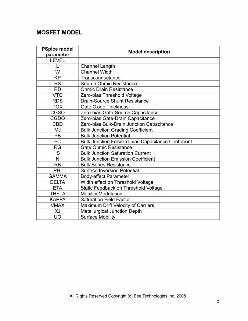
MOSFET MODEL
PSpice model parameter
Model description
LEVEL
L Channel Length
W Channel Width
KP Transconductance
RS Source Ohmic Resistance
RD Ohmic Drain Resistance
VTO Zero-bias Threshold Voltage
RDS Drain-Source Shunt Resistance
TOX Gate Oxide Thickness
CGSO Zero-bias Gate-Source Capacitance
CGDO Zero-bias Gate-Drain Capacitance
CBD Zero-bias Bulk-Drain Junction Capacitance
MJ Bulk Junction Grading Coefficient
PB Bulk Junction Potential
FC Bulk Junction Forward-bias Capacitance Coefficient
RG Gate Ohmic Resistance
IS Bulk Junction Saturation Current
N Bulk Junction Emission Coefficient
RB Bulk Series Resistance
PHI Surface Inversion Potential
GAMMA Body-effect Parameter
DELTA Width effect on Threshold Voltage
ETA Static Feedback on Threshold Voltage
THETA Mobility Modulation
KAPPA Saturation Field Factor
VMAX Maximum Drift Velocity of Carriers
XJ Metallurgical Junction Depth
UO Surface Mobility
All Rights Reserved Copyright (c) Bee Technologies Inc. 2008
3
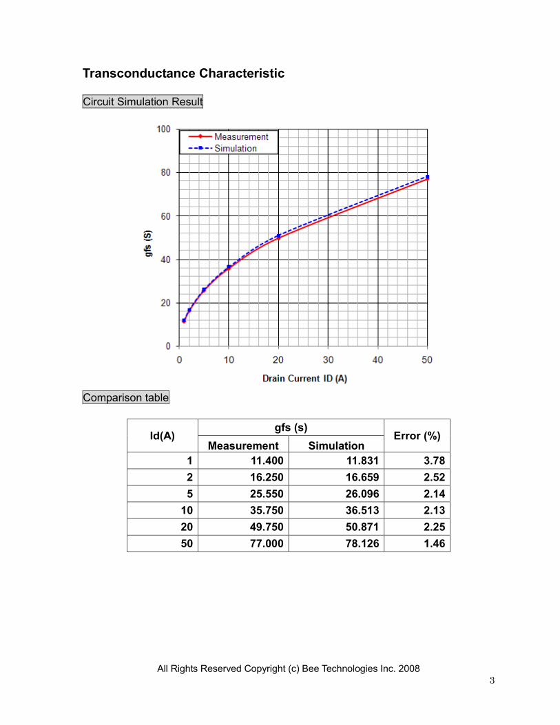
Transconductance Characteristic
Circuit Simulation Result
Comparison table
Id(A) gfs (s)
Error (%) Measurement Simulation
1 11.400 11.831 3.78
2 16.250 16.659 2.52
5 25.550 26.096 2.14
10 35.750 36.513 2.13
20 49.750 50.871 2.25
50 77.000 78.126 1.46

All Rights Reserved Copyright (c) Bee Technologies Inc. 2008
4
V1
0Vdc
V2
10
0
V3
0Vdc
U12SK3704
V_V1
0V 0.5V 1.0V 1.5V 2.0V 2.5V 3.0V 3.5V 4.0V 4.5V
I(V3)
0A
10A
20A
30A
40A
50A
60A
70A
80A
Vgs-Id Characteristic
Circuit Simulation result
Evaluation circuit
All Rights Reserved Copyright (c) Bee Technologies Inc. 2008
5
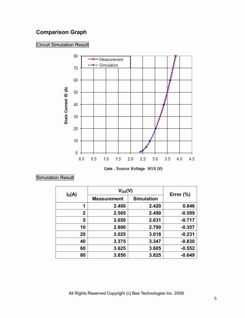
Comparison Graph Circuit Simulation Result
Simulation Result
ID(A) VGS(V)
Error (%) Measurement Simulation
1 2.400 2.420 0.846
2 2.505 2.490 -0.599
5 2.650 2.631 -0.717
10 2.800 2.790 -0.357
20 3.025 3.018 -0.231
40 3.375 3.347 -0.830
60 3.625 3.605 -0.552
80 3.850 3.825 -0.649
All Rights Reserved Copyright (c) Bee Technologies Inc. 2008
6
0
V3
0Vdc
VDS
0Vdc
V1
10
U12SK3704
V_VDS
0V 50mV 100mV 150mV 200mV 250mV
I(V3)
0A
5A
10A
15A
20A
25A
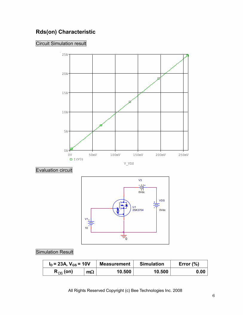
Rds(on) Characteristic
Circuit Simulation result
Evaluation circuit
Simulation Result
ID = 23A, VGS = 10V Measurement Simulation Error (%)
RDS (on) m 10.500 10.500 0.00
All Rights Reserved Copyright (c) Bee Technologies Inc. 2008
7
VDD
30
I1TD = 0
TF = 5nPW = 600uPER = 1000u
I1 = 0I2 = 1m
TR = 5n -
+
W1
ION = 0uAIOFF = 1mAW
I2
45
0
D2
DbreakU12SK3704
Time*1mA
0 10n 20n 30n 40n 50n 60n 70n
V(W1:3)
0V
5V
10V
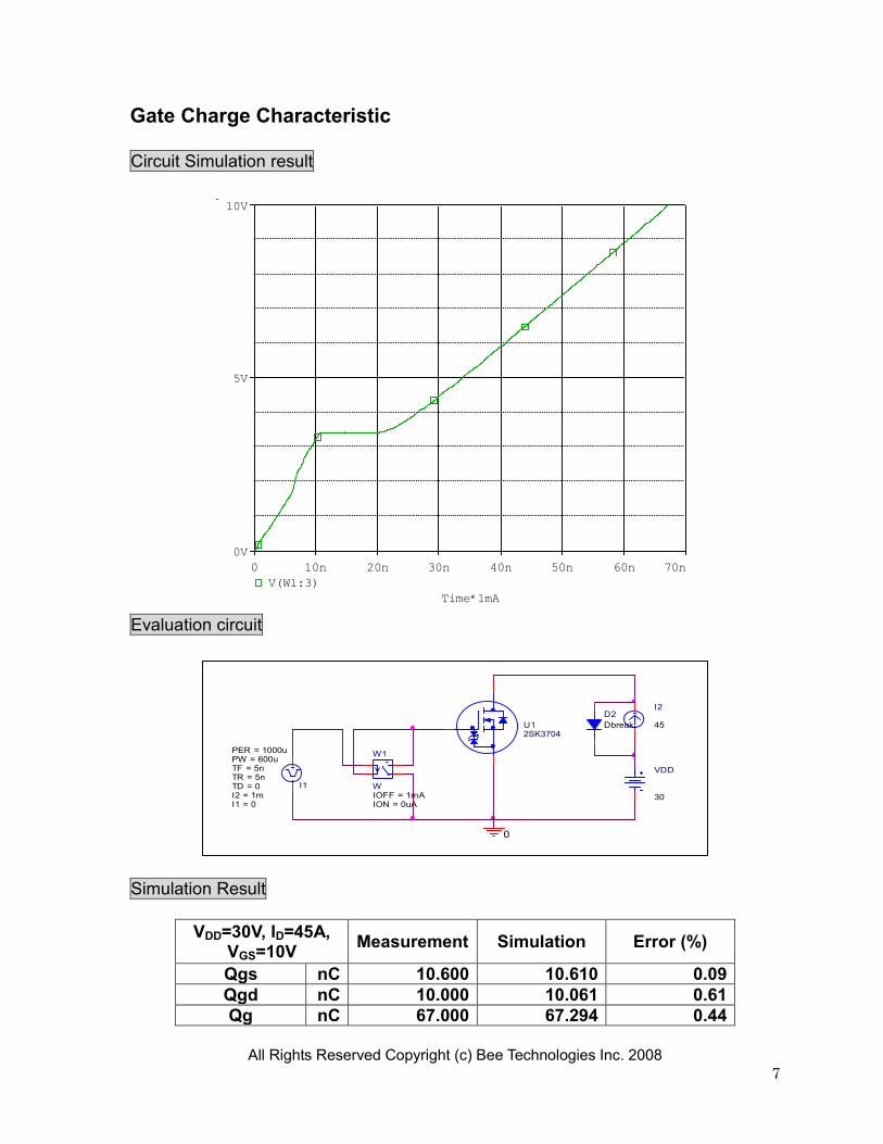
Gate Charge Characteristic Circuit Simulation result
Evaluation circuit
Simulation Result
VDD=30V, ID=45A, VGS=10V
Measurement Simulation Error (%)
Qgs nC 10.600 10.610 0.09
Qgd nC 10.000 10.061 0.61
Qg nC 67.000 67.294 0.44
All Rights Reserved Copyright (c) Bee Technologies Inc. 2008
8
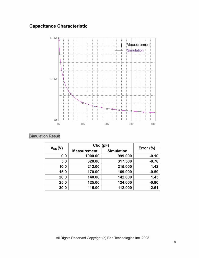
Capacitance Characteristic
Simulation Result
VDS (V) Cbd (pF)
Error (%) Measurement Simulation
0.0 1000.00 999.000 -0.10
5.0 320.00 317.500 -0.78
10.0 212.00 215.000 1.42
15.0 170.00 169.000 -0.59
20.0 140.00 142.000 1.43
25.0 125.00 124.000 -0.80
30.0 115.00 112.000 -2.61
Simulation
Measurement
All Rights Reserved Copyright (c) Bee Technologies Inc. 2008
9
0
VDD30Vdc
V2TD = 1u
TF = 5nPW = 10uPER = 20u
V1 = 0
TR = 5n
V2 = 20
U12SK3704
L2
50nH
R2
50
R1
50
L1
30nH
RL
1.3
Time
0.6us 0.8us 1.0us 1.2us 1.4us 1.6us
1 V(U1:G) 2 V(U1:D)
0V
2V
4V
6V
8V
10V
12V1
0V
20V
40V2
>>
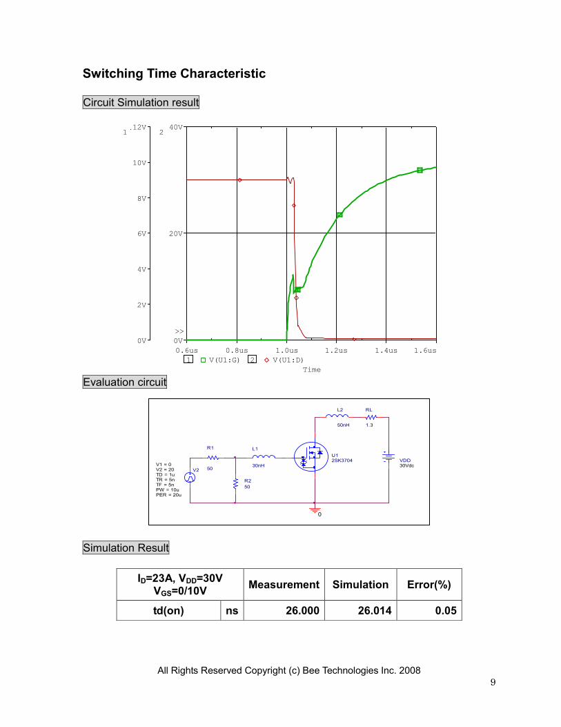
Switching Time Characteristic Circuit Simulation result
Evaluation circuit
Simulation Result
ID=23A, VDD=30V VGS=0/10V
Measurement Simulation Error(%)
td(on) ns 26.000 26.014 0.05
VGS
ID
All Rights Reserved Copyright (c) Bee Technologies Inc. 2008
10
V2
10V1
0
0
V3
0Vdc
U12SK3704
V_V2
0V 0.2V 0.4V 0.6V 0.8V 1.0V 1.2V 1.4V 1.6V 1.8V
I(V3)
0A
10A
20A
30A
40A
50A
60A
70A
80A
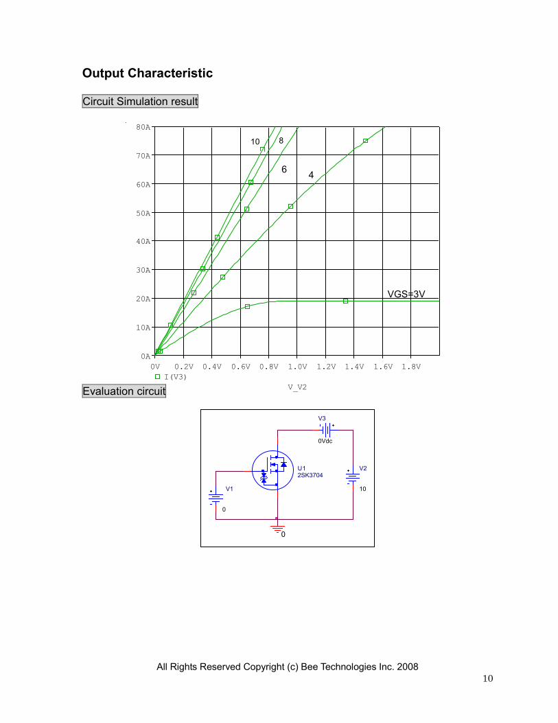
Output Characteristic
Circuit Simulation result
Evaluation circuit
VGS=3V
4
10
6 55
8
All Rights Reserved Copyright (c) Bee Technologies Inc. 2008
11
VSD
0
U12SK3704
Vsense
0Vdc
V_VSD
0V 0.3V 0.6V 0.9V 1.2V 1.5V
I(Vsense)
10mA
100mA
1.0A
10A
100A
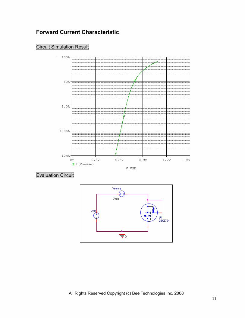
Forward Current Characteristic
Circuit Simulation Result
Evaluation Circuit
All Rights Reserved Copyright (c) Bee Technologies Inc. 2008
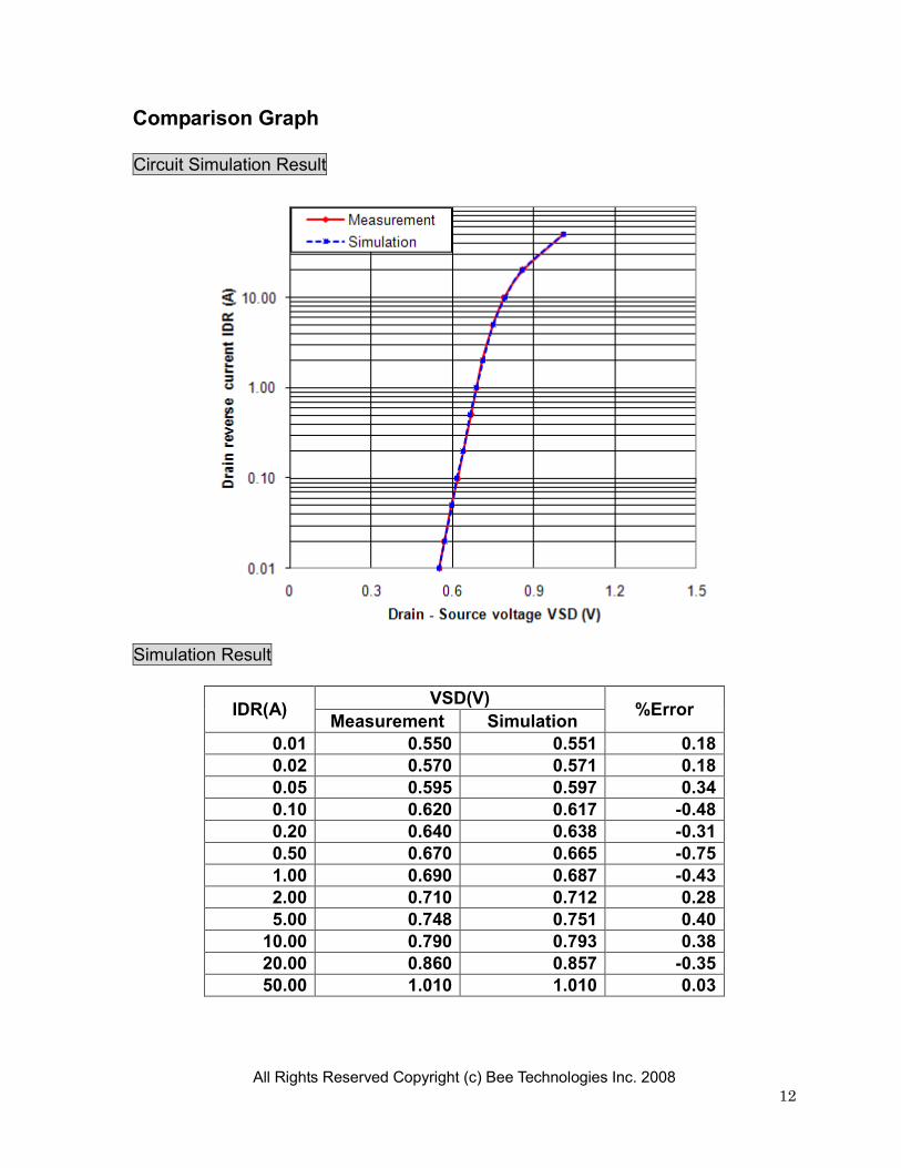
12
Comparison Graph Circuit Simulation Result
Simulation Result
IDR(A) VSD(V)
%Error Measurement Simulation
0.01 0.550 0.551 0.18
0.02 0.570 0.571 0.18
0.05 0.595 0.597 0.34
0.10 0.620 0.617 -0.48
0.20 0.640 0.638 -0.31
0.50 0.670 0.665 -0.75
1.00 0.690 0.687 -0.43
2.00 0.710 0.712 0.28
5.00 0.748 0.751 0.40
10.00 0.790 0.793 0.38
20.00 0.860 0.857 -0.35
50.00 1.010 1.010 0.03
All Rights Reserved Copyright (c) Bee Technologies Inc. 2008
13
V1
TD = 270ns
TF = 10nsPW = 20usPER = 50us
V1 = -9.45v
TR = 10ns
V2 = 10.65v
R1
50
0
U1D2SK3704
Time
19.4us 19.8us 20.2us 20.6us 21.0us 21.4us
I(R1)
-400mA
-300mA
-200mA
-100mA
-0mA
100mA
200mA
300mA
400mA
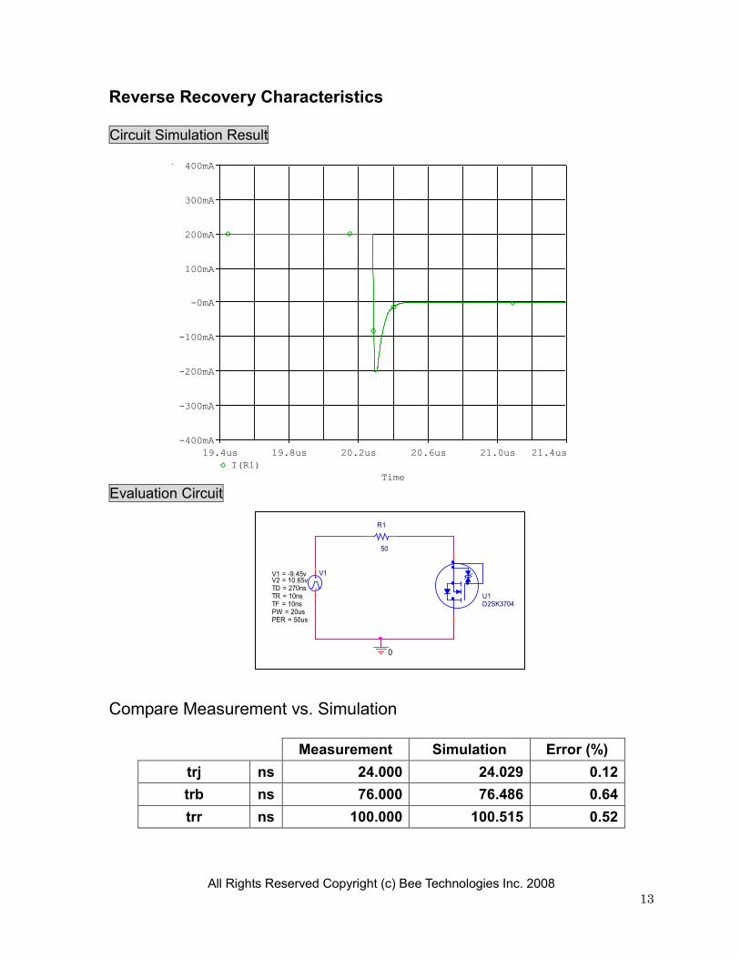
Reverse Recovery Characteristics Circuit Simulation Result
Evaluation Circuit
Compare Measurement vs. Simulation
Measurement Simulation Error (%)
trj ns 24.000 24.029 0.12
trb ns 76.000 76.486 0.64
trr ns 100.000 100.515 0.52
All Rights Reserved Copyright (c) Bee Technologies Inc. 2008
14
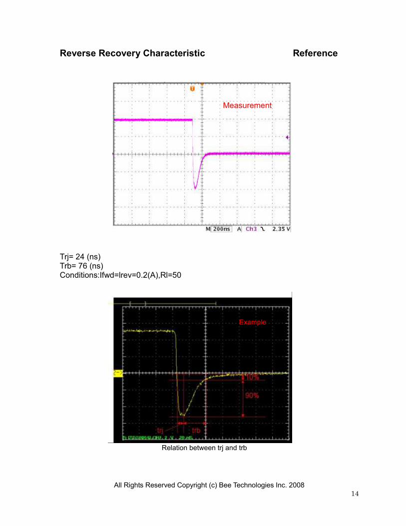
Reverse Recovery Characteristic Reference
Trj= 24 (ns) Trb= 76 (ns) Conditions:Ifwd=lrev=0.2(A),Rl=50
Relation between trj and trb
Example
Measurement
All Rights Reserved Copyright (c) Bee Technologies Inc. 2008
15
R1
0.001m
V1
0Vdc
0
U1
2SK3704R2
100MEG
V_V1
0V 5V 10V 15V 20V 25V 30V 35V 40V 45V 50V
I(R1)
0A
1mA
2mA
3mA
4mA
5mA
6mA
7mA
8mA
9mA
10mA
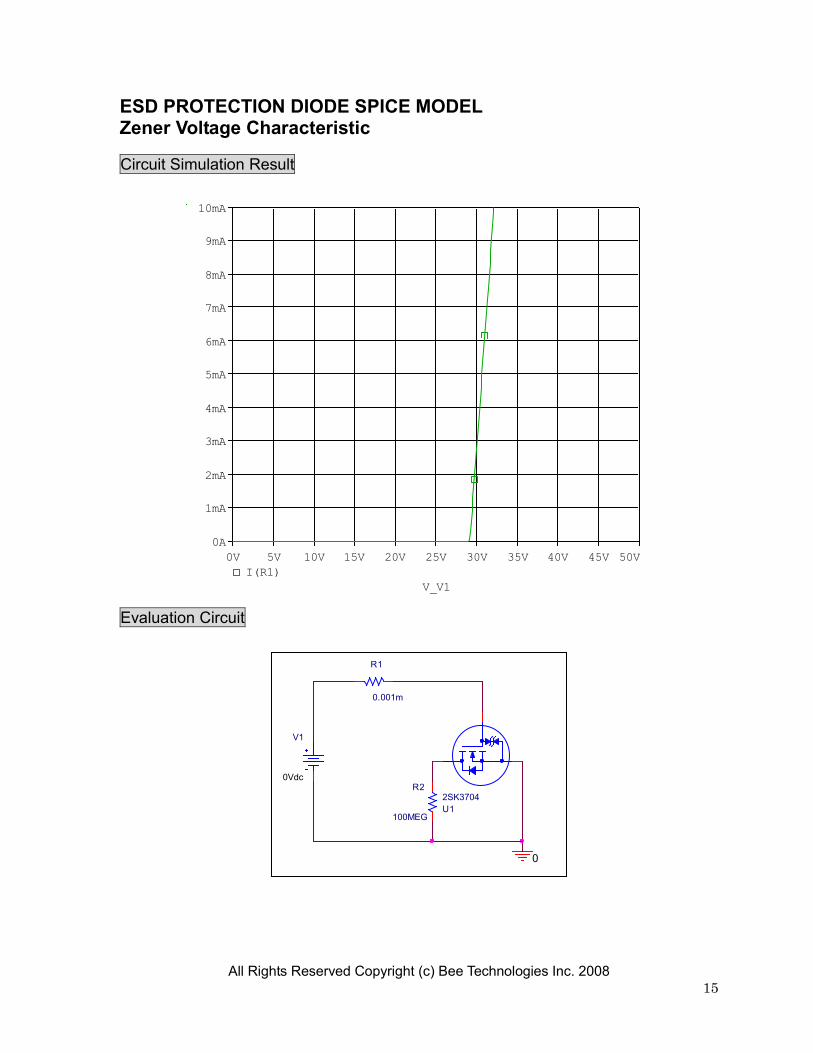
ESD PROTECTION DIODE SPICE MODEL
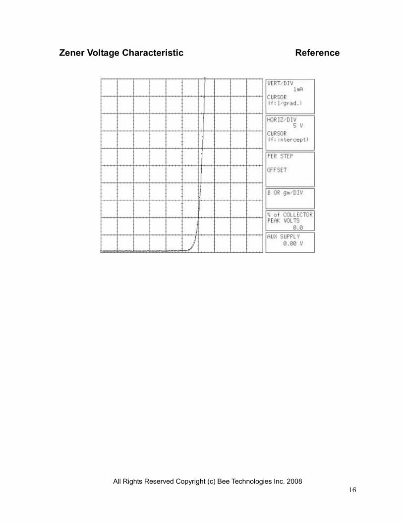
Zener Voltage Characteristic
Circuit Simulation Result
Evaluation Circuit
All Rights Reserved Copyright (c) Bee Technologies Inc. 2008
16
Zener Voltage Characteristic Reference