Embed Size (px)
Citation preview
APPLICATION NOTE [email protected]
Advanced Applications Enabled By OmniGIS® Gas Injection
Omniprobe’s OmniGIS® (Fig 1) is designed with enabling features to extend capability and results for typical gas processes within SEMs and FIBs in a manner not previously achievable, and in doing so, opens up new opportunities for in situ experiments within FIB and SEM instruments. One of the OmniGIS® key features includes three precursor gases delivered with a single needle. This approach allows mixing gases prior to their impinging the substrate (useful, for example, for flowing water with Pt to improve resistivity1 and ensures all gases occupy the same optimized port location for operations using a single gas or applying alternate gases in rapid succession). Another key feature is the capability to pulse the delivery valve, so the user has the option of running with the valve full open (100% duty cycle), or at a minimum duty cycle required to achieve the end result, thereby reducing overspray.
OmniGIS® Features
The OmniGIS® has two inert gas inlets that provide for inert gases to be operated as source gases or as carrier gases to assist transport of the precursor to the delivery site. These also act as purge gases that automatically clean the lines using a unique algorithm, determined by the phase of the source. The precursor temperatures can be adjusted from 0 to 40° C to achieve a working vapor pressure that does not have deleterious effects on the chamber vacuum. Pressure feedback control within the OmniGIS® itself ensures consistent and repeatable operation. The precursor crucible design is compatible with
AN-GIS-052411 © 2011 Omniprobe, Inc. All Rights Reserved
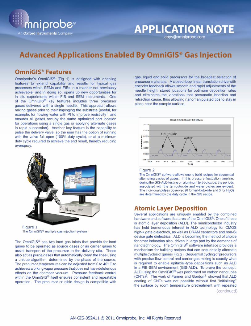
The OmniGIS® software allows one to build recipes for sequential alternating cycles of gases. In this pressure fluctuation timeline, during the GIS-ALD testing on aluminum tert-butoxide, the periods associated with the tert-butoxide and water cycles are evident. The individual pulses observed (6 for tert-butoxide and 3 for H2O) are determined by the duty cycle in the GIS recipe.
Figure 2
Figure 1The OmniGIS® multiple gas injection system
gas, liquid and solid precursors for the broadest selection of precursor materials. A closed-loop linear translation drive with encoder feedback allows smooth and rapid adjustments of the needle height, stored locations for optimum deposition rates and eliminates the vibrations that pneumatic insertion and retraction cause, thus allowing nanomanipulated tips to stay in place near the sample surface.
Atomic Layer DepositionSeveral applications are uniquely enabled by the combined hardware and software features of the OmniGIS®. One of these is atomic layer deposition (ALD). The semiconductor industry has held tremendous interest in ALD technology for CMOS high-k gate dielectrics, as well as DRAM capacitors and non-Si device gate dielectrics. ALD is becoming the method of choice for other industries also, driven in large part by the demands of nanotechnology. The OmniGIS® software interface provides a mechanism for building recipes that can sequentially alternate multiple cycles of gases (Fig. 2). Sequential cycling of precursors with precise flow control and carrier gas mixing is exactly what is required to enable epitaxial-type depositions such as ALD in a FIB-SEM environment (GIS-ALD). To prove the concept, ALD using the OmniGIS® was performed on carbon nanotubes (CNTs)2. The work of Farmer and Gordon3 showed that ALD coating of CNTs was not possible without first “initializing” the surface by room temperature pretreatment with repeated
(continued)
t-butoxidewater
Omniprobe - Dallas, TX 75238 - 214-572-6800AN-GIS-052411 © 2011 Omniprobe, Inc. All Rights Reserved
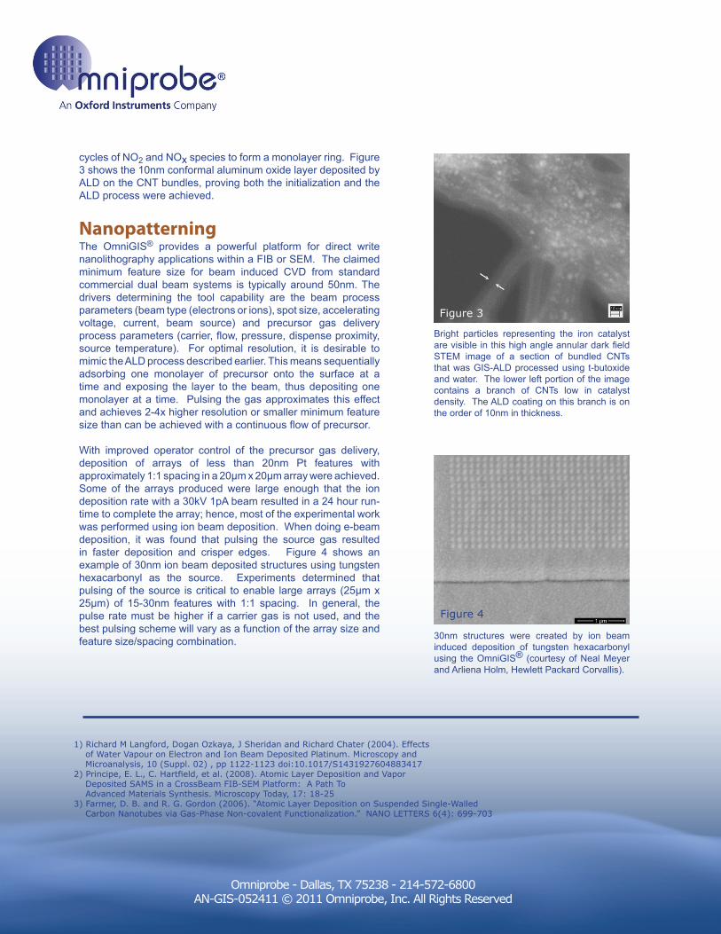
Bright particles representing the iron catalyst are visible in this high angle annular dark field STEM image of a section of bundled CNTs that was GIS-ALD processed using t-butoxide and water. The lower left portion of the image contains a branch of CNTs low in catalyst density. The ALD coating on this branch is on the order of 10nm in thickness.
Figure 3
Figure 4
30nm structures were created by ion beam induced deposition of tungsten hexacarbonyl using the OmniGIS® (courtesy of Neal Meyer and Arliena Holm, Hewlett Packard Corvallis).
cycles of NO2 and NOx species to form a monolayer ring. Figure 3 shows the 10nm conformal aluminum oxide layer deposited by ALD on the CNT bundles, proving both the initialization and the ALD process were achieved.
The OmniGIS® provides a powerful platform for direct write nanolithography applications within a FIB or SEM. The claimed minimum feature size for beam induced CVD from standard commercial dual beam systems is typically around 50nm. The drivers determining the tool capability are the beam process parameters (beam type (electrons or ions), spot size, accelerating voltage, current, beam source) and precursor gas delivery process parameters (carrier, flow, pressure, dispense proximity, source temperature). For optimal resolution, it is desirable to mimic the ALD process described earlier. This means sequentially adsorbing one monolayer of precursor onto the surface at a time and exposing the layer to the beam, thus depositing one monolayer at a time. Pulsing the gas approximates this effect and achieves 2-4x higher resolution or smaller minimum feature size than can be achieved with a continuous flow of precursor. With improved operator control of the precursor gas delivery, deposition of arrays of less than 20nm Pt features with approximately 1:1 spacing in a 20μm x 20μm array were achieved. Some of the arrays produced were large enough that the ion deposition rate with a 30kV 1pA beam resulted in a 24 hour run-time to complete the array; hence, most of the experimental work was performed using ion beam deposition. When doing e-beam deposition, it was found that pulsing the source gas resulted in faster deposition and crisper edges. Figure 4 shows an example of 30nm ion beam deposited structures using tungsten hexacarbonyl as the source. Experiments determined that pulsing of the source is critical to enable large arrays (25μm x 25μm) of 15-30nm features with 1:1 spacing. In general, the pulse rate must be higher if a carrier gas is not used, and the best pulsing scheme will vary as a function of the array size and feature size/spacing combination.
Nanopatterning
1) Richard M Langford, Dogan Ozkaya, J Sheridan and Richard Chater (2004). Effects of Water Vapour on Electron and Ion Beam Deposited Platinum. Microscopy and Microanalysis, 10 (Suppl. 02) , pp 1122-1123 doi:10.1017/S14319276048834172) Principe, E. L., C. Hartfield, et al. (2008). Atomic Layer Deposition and Vapor Deposited SAMS in a CrossBeam FIB-SEM Platform: A Path To Advanced Materials Synthesis. Microscopy Today, 17: 18-253) Farmer, D. B. and R. G. Gordon (2006). “Atomic Layer Deposition on Suspended Single-Walled Carbon Nanotubes via Gas-Phase Non-covalent Functionalization.” NANO LETTERS 6(4): 699-703