Embed Size (px)
Citation preview

www.smthelp.com
1. Film Generation
2. Shear Raw Material
3. Drill Holes
Industry standard 0.059" thick, copper clad, two sides

www.smthelp.com
4. Electrolus copper
Apply copper in hole barrels
5. Apply Image
Apply Photosensitive Material to develop selected areas from panel
www.smthelp.com
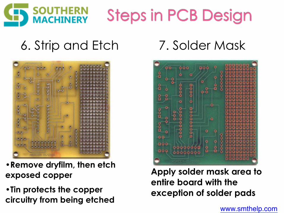
6. Strip and Etch
•Remove dryfilm, then etch exposed copper •Tin protects the copper circuitry from being etched
7. Solder Mask
Apply solder mask area to entire board with the exception of solder pads

www.smthelp.com
8. Solder Coat 9. Silkscreen
Apply white letter marking using screen printing process
Apply solder to pads

www.smthelp.com
PCB Design and Manufacture
FR14122440W
Layer count:Double side
Material: FR-4/1.2
Puzzle size:149.75*100.36mm/4
Surface finished: lead-free
Panel size: 37.11*93.8mm/1
Characteristics: Rogers multilayer PCB with impedance control
Lead time: 2 weeks Price: $1.3/board FOB Shenzhen
FR14122440W

www.smthelp.com
Welcome inquiry1,Please visit : www.smthelp.com
2, Find us more: https://www.facebook.com/autoinsertion
3, Know more our team: https://cn.linkedin.com/in/smtsupplier
4, Welcome to our factory in Shenzhen China
5, See more machine working video, please Youtube: Auto Insertion
6, Google: Auto+insertion, to get more informations
7,Looking forward to your email: [email protected]