Embed Size (px)
Citation preview

Prepared By
SANA ULLAHM.cs
Roll No - 35854 Student Contact No - +923219316714 Hazara university Mansehra IT department

Moore’s Law
Given by Gordon Moore in 1965, co-founder and former chairman of Intel Corporation.
It states : The number of transistors that can be placed inexpensively on an integrated circuit doubles approximately every two years.
This trend has continued for more than half a century and is expected to continue until 2015 or 2020 or later.

Microprocessor• The microprocessor is the core of computer
systems.- Nowadays many communication, digital
entertainment, portable devices, are controlled by them.
- The word comes from the combination micro and processor.

Processor
- Processor means a device that processes whatever. In this context processor means a device that processes numbers, specifically binary numbers, 0’s and 1’s.
- In the late 1960’s, processors were built using discrete elements. These devices performed the required operation, but were too large and too slow.

Micro
- In the early 1970’s the microchip was invented. All of the components that made up the processor were now placed on a single piece of silicon. The size became several thousand times smaller and the speed became several hundred times faster. The “Micro” Processor was born.

Definition of a Microprocessor
• The microprocessor is a programmable device that takes in numbers, performs on them arithmetic or logical operations according to the program stored in memory and then produces other numbers as a result.

First CPU on 1 chip• Intel 4004 :
o First single-chip microprocessor.o Developed by Ted Hoff, Masatoshi Shimao Introduced November 15, 1971o 16-pin microprocessoro Clock rate 740 kHz.
o Around 70,000 instructions per second.o Number of Transistors 2,300 at 10 µmo Main memory 640 byteso Programme can store 4kbo Bus Width 4-bits and 4-bits registero Originally designed to be used in japanese Busicom 141-pf
calculator

Busicom 141-pf printer calculator

Intel 4004 Picture

Clock rateIt refers to the frequency .The speed at which microprocessor execute instructions per second.It can be measured in hz,khz,mhz,ghz…old unit was cp/s mean cycle per second.Transistora transistor is an electronic component used in a circuit to control a large amount of current or voltage with a small amount of voltage or current.RegisterIn a computer, a register is one of a small set of data holding places that are part of a computer processor.

A register may hold a computer instruction, a storage address, or any kind of data (such as a bit sequence or individual characters). Some instructions specify registers as part of the instruction. For example, an instruction may specify that the contents of two defined registers be added together and then placed in a specified register. A register must be large enough to hold an instruction - for example, in a 32-bit instruction computer, a register must be 32 bits in length. In some computer designs, there are smaller registers - for example, half-registers - for shorter instructions. Depending on the processor design and language rules, registers may be numbered or have arbitrary names.

System busProvides for communication among processors, main memory, and I/O modules.Data busBus is defined to transfer data b/w hardware component of Computer. It is the process within CPU to send data to processor or send data from processor. Internal buses carry information within processor while external buses carry information or data b/w processor and Memory.The width of data bus refers to number of bits commonly this width include 4,8,16,32 and 64.A 64-line data bus can transfer 64 bits of data at one time.The data bus lines are bi-directional. It means that:1)CPU can read data from memory using these lines2)CPU can write data to memory locations using these line

Address busIt has bits address where data should reach from actual Position. Many components are connected to one another through buses. Each component is assigned a unique ID. This ID is called the address of that component. It a component wants to communicate with another component, it uses address bus to specify the address of that component. The address bus is a unidirectional bus. It can carry information only in one direction. It carries address of memory location from microprocessor to the main memory.The width of the address bus determines the amount of memory that can be addressed. A 32-bit bus can address 4,294,967,296 (2 ^ 32) bytes of memory.

Control BusControl bus is used to transmit different commands or control signals from one component to another component. Suppose CPU wants to read data from main memory. It will use control is also used to transmit control signals like ASKS (Acknowledgement signals). A control signal contains the following:1 Timing information: It specifies the time for which a device can use data and address bus.2 Command Signal: It specifies the type of operation to be performed.Suppose that CPU gives a command to the main memory to write data. The memory sends acknowledgement signal to CPU after writing the data successfully. CPU receives the signal and then moves to perform some other action.

Main memoryMain memory is where programs and data are kept when the processor is actively using them. When programs and data become active, they are copied from secondary memory into main memory where the processor can interact with them. A copy remains in secondary memory.
Secondary memorySecondary memory is where programs and data are kept on a long-term basis. Common secondary storage devices are the hard disk and . The hard disk has enormous storage capacity compared to main memory.

Intel 8008Introduced in April 1972.
It was first 8-bit µP.
16-pin microprocessor
Its clock rate 500 KHz-800khz.
Could execute 36,000-80,000 instructions per second.
Number of Transistors 2,300 at 10 µm
Programme memory space 16kb
Bus width 8 bits and 8 bits of register
used in Mark-8 computer which was 1st Pc

Mark-8 computer

Intel 8008

Intel 8080Introduced in April 1974.
designed by Federico Faggin and Masatoshi Shima
It was also 8-bit µP.
40-pin microprocessor
its clock speed was 2 MHz.
It had 6,000 transistors at 6 µm.
Was 10 times faster than 8008.
Could execute 5,00,000 instructions per second
Programme memory space 64kb
16-bit address bus and an 8-bit data bus and register

Intel 8080

Intel 8085Introduced in 1976.
40-pin microprocessor
It was also 8-bit µP.
Its clock speed was 3 ,5,and 6MHz.
its data bus is 8-bit and address bus is 16-bit.
It had 6,500 transistors at 3 micrometer
Could execute 7,69,230 instructions per second.
It could access 64 KB of memory.

Intel 8085

Intel 8086Introduced in 8 june 1978.
It was first 16-bit µP.
40-pin microprocessor
Its clock speed is 4.77 MHz, 8 MHz and 10 MHz, depending on the version.
Its data bus and register is 16-bit and address bus is 20-bit.
It had 29,000 transistors at 3µm.
Could execute 2.5 million instructions per second.
It could access 1 MB of memory.
It had multiply and divide instructions.
Used in portable computing.

Intel 8086

Intel 8088Introduced in 1 june 1979.
Its clock rate 5mhz-10mhz
40-pin processor
It had 45,000 transistors at 6µm
It was also 16-bit µP. 16-bit register and data bus and 20 bits of address bus
It was created as a cheaper version of Intel’s 8086.
Could execute 2.5 million instructions per second.
This chip became the most popular in the computer industry when IBM used it for its first PC.

Intel 8088

Intel 80386Introduced October 17, 1985.Clock rates : 16 – 33 MHz.32-bit data & address busSpace memory 4GBVirtual Memory 64 TBNo. of transistors : 275,000 at1 µmUsed in Desktop Computing

80188 and 80186
Introduced in 1982.
They were 16-bit µPs.
Clock speed was 6 MHz.
80188 was a cheaper version of 80186 with an 8-bit external data bus.
No of transistors 55000 at 3 µm

Intel 80286
1982 Clock speed: 12 MHz
Number of transistor:• 134000 at 1.5 µm• 16-bit register and data bus• It could execute 4 million instructions per
second.

Intel 80286

Intel 80386 Introduced in 17 october 1985.
It was first 32-bit µP.
Its data bus is 32-bit and address bus is 32-bit.
It could address 4 GB of memory.
It had 2,75,000 transistors at 1.5 µm
Its clock speed varied from 16 MHz to 33 MHz depending upon the various versions.
Different versions: 80386 DX
80386 SX
80386 SL
Intel 80386 became the best selling microprocessor in history
Used in Desktop Computing

Intel 80386
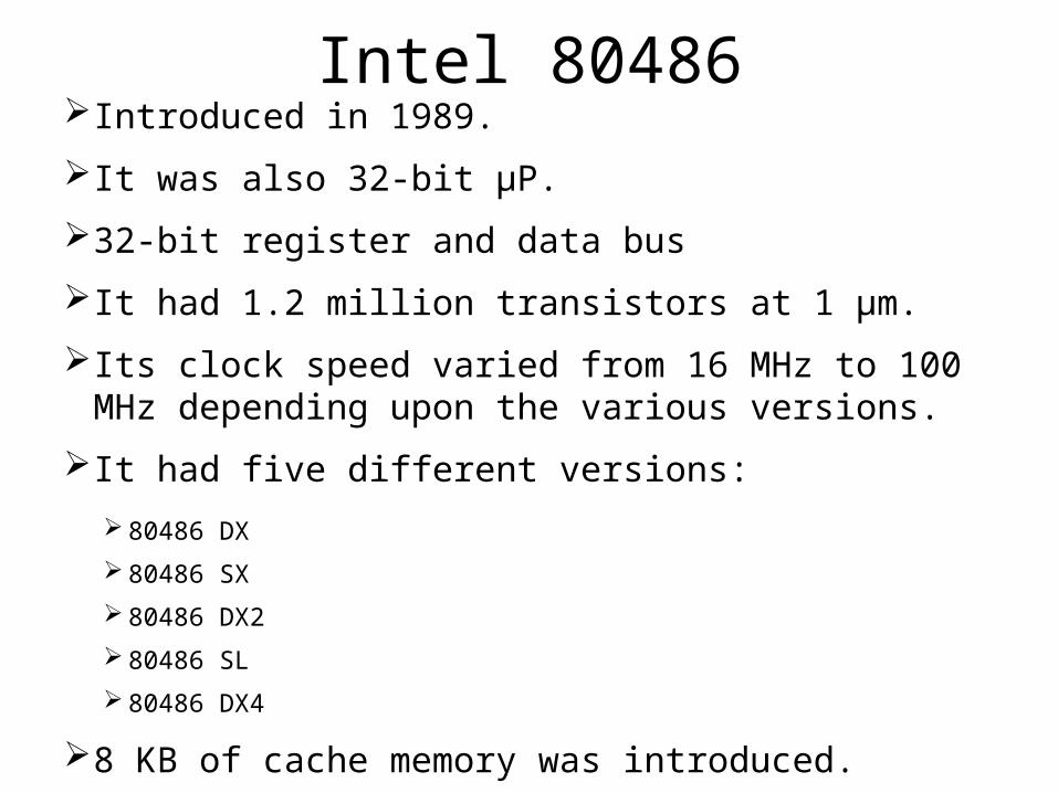
Intel 80486 Introduced in 1989.
It was also 32-bit µP.
32-bit register and data bus
It had 1.2 million transistors at 1 µm.
Its clock speed varied from 16 MHz to 100 MHz depending upon the various versions.
It had five different versions:
80486 DX
80486 SX
80486 DX2
80486 SL
80486 DX4
8 KB of cache memory was introduced.

Intel 80486

cache memory
cache memory is a high speed memory kept in between processor and RAM to increase the data execution speed. It is kept near to the processor. This is also know as high speed buffer.L1-cacheL1-cache is the fastest cache and it usually comes within the processor chip itself. The L1 cache typically ranges in size from 8KB to 64KB and uses the high-speed SRAM (static RAM) instead of the slower and cheaper DRAM (dynamic RAM) used for main memory.

L2-cacheThis is not on the processor.L2 cache comes between L1 and RAM(processor-L1-L2-RAM) and is bigger than the primary cache (typically 64KB to 4MB).L3-cacheL3 caches are found on the motherboard rather than the processor. It is kept between RAM and L2 cache.
So if your system has L1,L2 and L3 cache data fetching will be L1->L2->L3->RAM ie. If data is not there in L1 it will check L2 then L3 then RAM...

Intel pentium 1 Introduced in in 22 march 1993.
It was also 32-bit µP.
It had 3100,000 (3.1million) transistors at 0.8µm.
It was originally named 80586.
Its clock speed was 66 MHz.
Its data bus and register is 32-bit and address bus is 32-bit.
It could address 4 GB of memory.
Virtual Memory 64 TB
Could execute 110 million instructions per second.
Cache memory is of 16 KB:
8 KB for instructions. 8 KB for data.

Intel pentium 1

Intel pentium Pro Introduced in 1995.
It was also 32-bit µP.
It had 5500,000 (5.5million) transistors at 0.5µm.
It had L2 cache of 256 KB.
It had 21 million transistors.
*32-bit register and data bus
It was primarily used in server systems.
Cache memory: 8 KB for instructions.
8 KB for data.
It had L2 cache of 256 KB.

Intel pentium Pro
Intel pentium II Introduced in 8 january 1997.
It was also 32-bit µP.
32-bit register and data bus.
No. of transistors : 7500,000 at 0.35 µm
Its clock speed was 233 MHz to 500 MHz.
Could execute 333 million instructions per second.
32 KB L1 cache
MMX technology was supported.

Intel pentium II

Intel Pentıum III
Introduced in 1999.
It was also 32-bit µP.
Introduction of L2 cache (512 KB)
Its clock speed varied from 500 MHz to 1.4 GHz.
32-bit register and data bus
It had 9.5 million transistors at 0.25µm.

Intel Pentıum III

Intel Pentıum IV
Introduced in 2000.
64-bit register and data bus.
Its clock speed was from 1.3 GHz to 3.8 GHz.
L2 cache increased upto 512 KB
All internal connections were made from aluminium to copper.
Used greatly in the desktop & laptop computers.
No. of transistors : 42 million at 0.18 µm

Intel Pentıum IV

Intel Dual Core Introduced in 2006.
It is 32-bit or 64-bit µP.
Its clock speed was from 1.3 GHz to 2.6 GHz
No of transistors 1,700,000,000 at 90 nm.
It has two cores.
Both the cores have there own internal bus and L1 cache, but share the external bus and L2 cache .
It supported SMT technology.
SMT: Simultaneously Multi-Threading
E.g.: Adobe Photoshop supported SMT
Intel Dual Core

Intel Core 2 Introduced in 2006.
It is a 64-bit µP.
Its clock speed is from 1.2 GHz to 3 GHz.
It has 291 million transistors.
It has 64 KB of L1 cache per core and 4 MB of L2 cache.
It is launched in three different versions: Intel Core 2 Duo
Intel Core 2 Quad
Intel Core 2 Extreme