Embed Size (px)
Citation preview
Organic Light Emitting Diode ….Technology in a Slim & Flexible way By- Snehasis Mondal, Stream- ECE(B) Roll-86 Year-2013- 2017 Paper-HU-491 March,2015
1 | P a g e
Organic
Light
Emitting
Diode ….Technology in a Slim & Flexible way
Presented for-
Techno India, Salt Lake, Humanities Dpt.
2 | P a g e
Certificate
This is to certify that the project entitled “Organic Light Emitting Diode "embodies the
original work done by Snehasis Mondal in partial fulfilment for the bachelor's degree in
Electronics & Communication Engineering during the year 2014-15 as prescribed by Techno
India,Saltlake, Humanities department.
Place:
Date: Signature
3 | P a g e
Acknowledgement
A report on a technical topic like OLED helps people to realise how much he owe to
google,Wikipedia,youtude & Microsoft word spelling checker. I acknowledge with thanks the support by my
friend Raj Krishan Ghosh for helping me with information about the experiment, as well as with mental
support.
I like to thank all the teachers of ECE department, especially Asit Kumar Datta, Head of the Department of
ECE, Salt Lake for his encouragement & help on the research purpose of the topic.
I am extremely grateful to Mrs Rituporna Ghosh of techno India, Salt Lake, Humanities Department for her
encouragement for the report & for her help with the data regarding the report writing. My heartfelt thanks
to the two living god of mine my mom & dad.
-Snehasis Mondal
4 | P a g e
Table of Contents
Abstract 5
Summery 6-7
Preface 8
Introduction 10 Discussion:
History 11 General Lighting Source 12 Architecture of OLED 13 OLED Fabrication 14-15 Working Principle 16-17 Various types of OLED 18-20
Advantages of OLED 21
Disadvantages of OLED 22 Manufacturing & Commercial Use 23-24
Conclusion 25 Recommendation 26 References 27 Glossary 28
5 | P a g e
Abstracts
OLED is a display device that sandwiches carbon based films of organic molecules that is 100 to 500 nanometres thick between the two electrodes and when voltage is applied creates light. This is a very essential technology for our near future.
OLED doesn’t require any backlight. i.e., they are self-emitting. It emits its own light.OLEDs are made from carbon and hydrogen. As the OLEDs are made of organic compounds, they are called as Organic Light
Emitting Diode.OLEDs have dynamic power consumption when displaying different images.
The power consumption of the OLED panel is only dependent on the pixels that are lit in the images.
6 | P a g e
Summery An organic light emitting diode (OLED) is a light-emitting diode (LED) in which the emissive
electroluminescent layer is a film of organic compounds which emit light in response to an electric current. This layer of organic semiconductor material is situated between two electrodes. Generally, at least one of
these electrodes is transparent.
A typical OLED is composed of a layer of organic materials situated between two electrodes, the anode and cathode, all deposited on a substrate. The organic molecules are electrically conductive as a result of delocalization of pi electrons caused by conjugation over all or part of the molecule. These materials have conductivity levels ranging from insulators to conductors, and therefore are considered organic
semiconductors. The highest occupied and lowest unoccupied molecular orbitals (HOMO and LUMO) of organic semiconductors are analogous to the valence and conduction bands of inorganic semiconductors. Originally, the most basic polymer OLEDs consisted of a single organic layer. However multilayer OLEDs can be fabricated with two or more layers in order to improve device efficiency. Many modern OLEDs incorporate a simple bilayer structure, consisting of a conductive layer and an emissive layer.
During operation, a voltage is applied across the OLED such that the anode is positive with respect to the
cathode. A current of electrons flows through the device from cathode to anode, as electrons are injected into the LUMO of the organic layer at the cathode and withdrawn from the HOMO at the anode. This latter
process may also be described as the injection of electron holes into the HOMO. Electrostatic forces bring the electrons and the holes towards each other and they recombine forming an exciton, a bound state of
the electron and hole. This happens closer to the emissive layer, because in organic semiconductors hol es are generally more mobile than electrons. The decay of this excited state results in a relaxation of the energy levels of the electron, accompanied by emission of radiation whose frequency is in the visible region. The frequency of this radiation depends on the band gap of the material, in this case the difference in energy between the HOMO and LUMO.
Molecules commonly used in OLEDs include organometallic chelates (for example Alq3, used in the organic light-emitting device reported by Tang et al.), fluorescent and phosphorescent dyes and conjugated
dendrimers. A number of materials are used for their charge transport properties, for example triphenylamine and derivatives are commonly used as materials for hole transport layers. Fluorescent dyes
can be chosen to obtain light emission at different wavelengths, and compounds such as perylene, rubrene and quinacridone derivatives are often used. Alq3 has been used as a green emitter, electron transport
material and as a host for yellow and red emitting dyes. The production of small molecule devices and displays usually involves thermal evaporation in a vacuum.
This makes the production process more expensive and of limited use for large-area devices than other
processing techniques. However, contrary to polymer-based devices, the vacuum deposition process
enables the formation of well controlled, homogeneous films, and the construction of very complex multi -
layer structures. This high flexibility in layer design, enabling distinct charge transport and charg e blocking
layers to be formed, is the main reason for the high efficiencies of the sm all molecule OLEDs.
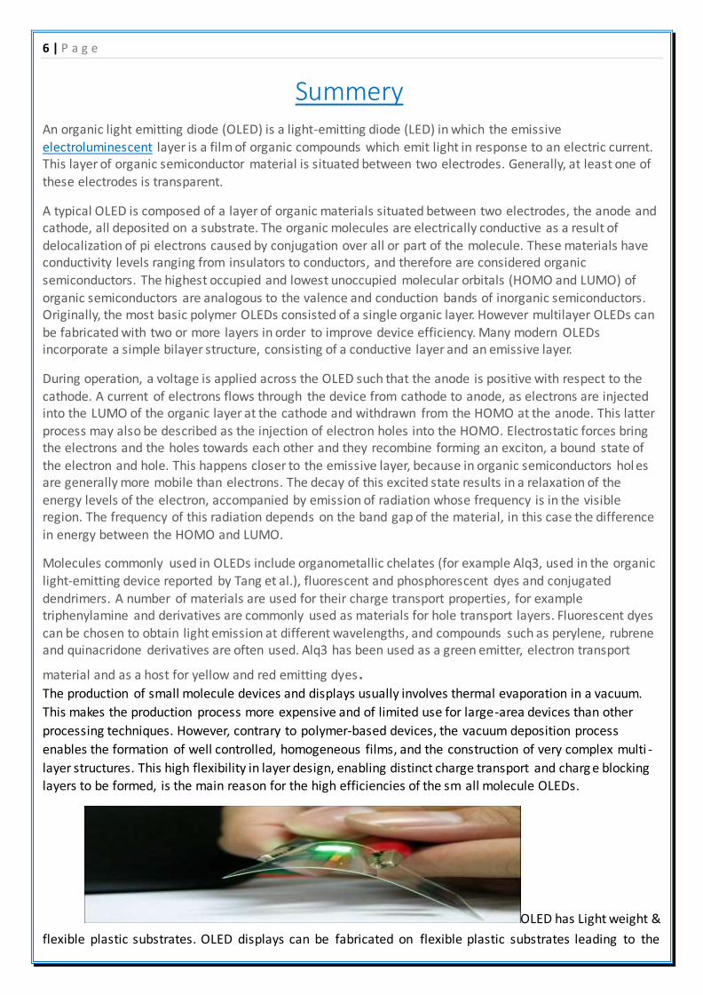
OLED has Light weight &
flexible plastic substrates. OLED displays can be fabricated on flexible plastic substrates leading to the
7 | P a g e
possibility of flexible organic light-emitting diodes being fabricated or other new applications such as roll-up
displays embedded in fabrics or clothing. As the substrate used can be flexible, the displays may be produced
inexpensively. OLEDs can also have a faster response time than standard LCD screens. Whereas LCD displays
are capable of between 2 and 8 ms response time offering a frame rate of +/-200 Hz, an OLED can
theoretically have less than 0.01 ms response time enabling 100,000 Hz.
OLED technology promises to revolutionize everything known about information display, from video walls, to dynamic pricing in supermarkets. For the military, Top-emitting OLED (TOLED) applications could include
wrist-mounted, featherweight, rugged PDAs and wearable electronic displays such as "display sleeves" Other applications could be conformed, high-contrast automotive instrument panels, windshield displays and visor mounted displays to be used by for pilots, drivers and divers, etc. More futuristic applications could be utilized in camouflage systems, "smart" light emitting windows/shades etc.
8 | P a g e
Preface
Organic Light Emitting Diode is a very essential technology for our near future. It consumes less energy than any other display available in the market. Though the research on OLED is in progress, but it has a huge potential to give world a better technology in terms of environmental degradation. OLED screens are self-emitting. So the size of the display screen of it, is very slim. Nowadays as the technology is growing we are looking for technologies, that comes in slim size .OLED gives this opportunities to make the screens in
blade like thickness.
OLED have a flexible aspect too. Companies like Samsung, L.G, and Motorola are trying to make a commercial flexible OLED display.
OLEDs have a great aspect on future’s electronics research .So, here the research work on OLED have done
on this report. This report contents the details about OLED. It gives idea about how does OLED works. Here the types of OLEDs, advantages & disadvantages of using OLEDs are discussed. Discussion on the reach
work going on worldwide basis, future &past of OLEDs have been done here .Hope this will help to understand & stimulate enthusiasm about OLEDS.
9 | P a g e
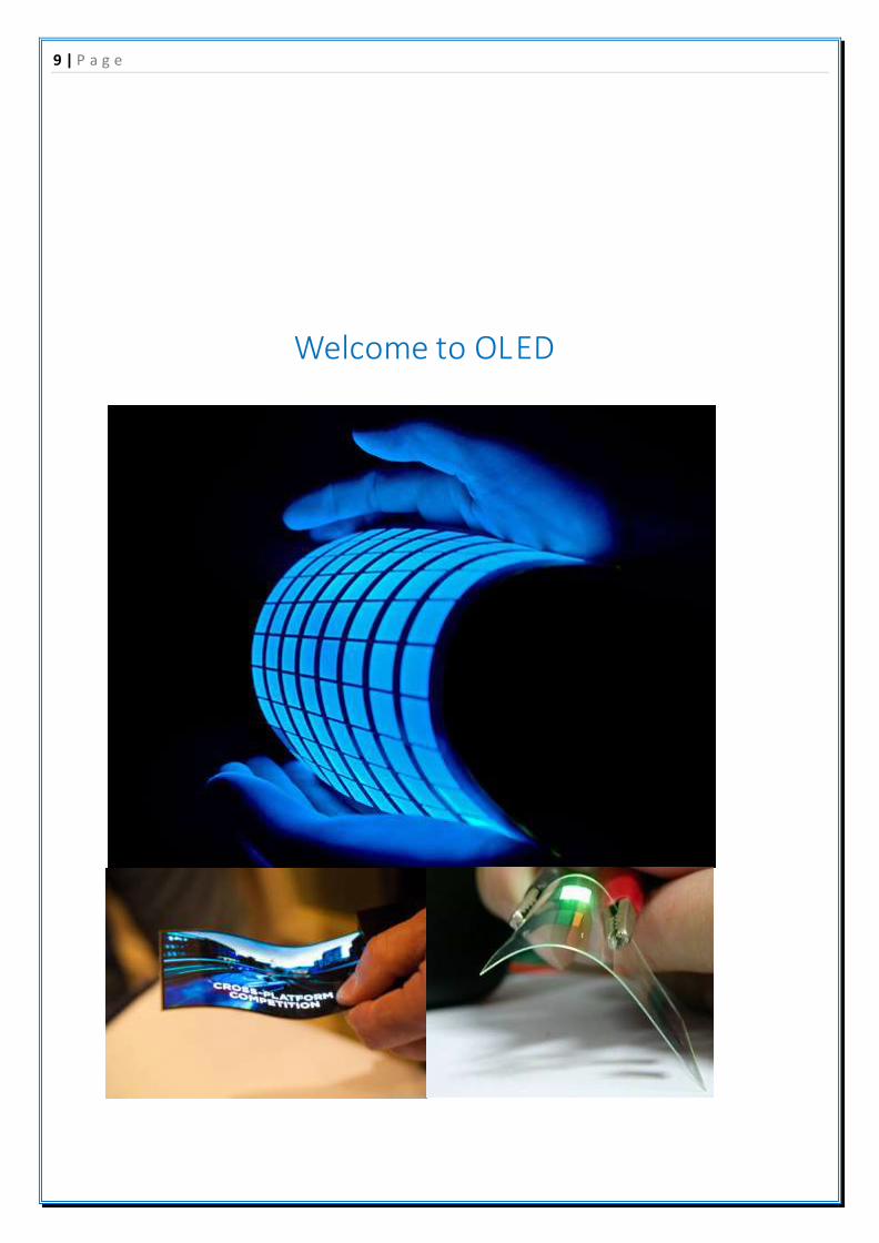
Welcome to OL ED
10 | P a g e
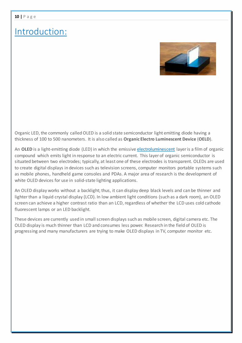
Introduction:
Organic LED, the commonly called OLED is a solid state semiconductor light emitting diode having a thickness of 100 to 500 nanometers. It is also called as Organic Electro Luminescent Device (OELD).
An OLED is a light-emitting diode (LED) in which the emissive electroluminescent layer is a film of organic
compound which emits light in response to an electric current. This layer of organic semiconductor is situated between two electrodes; typically, at least one of these electrodes is transparent. OLEDs are used
to create digital displays in devices such as television screens, computer monitors portable systems such as mobile phones, handheld game consoles and PDAs. A major area of research is the development of
white OLED devices for use in solid-state lighting applications.
An OLED display works without a backlight; thus, it can display deep black levels and can be thinner and
lighter than a liquid crystal display (LCD). In low ambient light conditions (such as a dark room), an OLED
screen can achieve a higher contrast ratio than an LCD, regardless of whether the LCD uses cold cathode
fluorescent lamps or an LED backlight.
These devices are currently used in small screen displays such as mobile screen, digital camera etc. The
OLED display is much thinner than LCD and consumes less power. Research in the field of OLED is progressing and many manufacturers are trying to make OLED displays in TV, computer monitor etc.
11 | P a g e
History: The first observations of electroluminescence in organic materials were in the early 1950s by André
Bernanos and co-workers at the Nancy-University in France. They applied high alternating voltages in air to materials such as acridine orange, either deposited on or dissolved in cellulose or cellophane thin films.
The proposed mechanism was either direct excitation of the dye molecules or excitation of electrons.
In 1960, Martin Pope and some of his co-workers at New York University developed ohmic dark-injecting
electrode contacts to organic crystals. They further described the necessary energetic requirements (work functions) for hole and electron injecting electrode contacts. These contacts are the basis of c harge injection in all modern OLED devices. Pope's group also first observed direct current (DC)
electroluminescence under vacuum on a single pure crystal of anthracene and on anthracen crystals doped
withtetracene in 1963 using a small area silver electrode at 400 volts. The proposed mechanism was field-accelerated electron excitation of molecular fluorescence. Pope's group reported in 1965that in the absence of an external electric field, the electroluminescence in anthracene crystals is caused by the recombination of a thermalized electron and hole, and that the conducting level of anthracene is higher in
energy than the excitation energy level. Also in 1965, W. Helfrich and W. G. Schneider of the National
Research Council in Canada produced double injection recombination electroluminescence for the first time in an anthracene single crystal using hole and electron injecting electrodes, the forerunner of modern
double injection devices. In the same year, Dow Chemical researchers patented a method of preparing electroluminescent cells using high voltage (500–1500 V) AC-driven (100–3000 Hz) electrically insulated
one millimetre thin layers of a melted phosphor consisting of ground anthracene powder, tetracene, and graphite powder. Their proposed mechanism involved electronic excitation at the contacts between
the graphite particles and the anthracene molecules. Electroluminescence from polymer films was first
observed by Roger Partridge at the National Physical Laboratory in the United Kingdom. The device consisted of a film of poly (N-vinylcarbazole) up to 2.2 micrometres thick located between two charge
injecting electrodes. The results of the project were patented in 1975 and published in 1983.
The first diode device was reported at Eastman Kodak by Ching W. Tang and Steven Van Slykein 1987. This device used a novel two-layer structure with separate hole transporting and electron transporting layers such that recombination and light emission occurred in the middle of the organic layer; this resulted in a
reduction in operating voltage and improvements in efficiency that led to the current era of OLED research and device production. Research into polymer electroluminescence culminated in 1990 with J. H.
Burroughs et al. at the Cavendish Laboratory in Cambridge reporting a high efficiency green light-emitting polymer based device using 100 nm thick films of poly(p-phenylene vinylene)
In 1996 pioneer produces world’s first PMOLED .In 2000 companies like L.G,MOTOROLA developed various displays .SONY developed world’s first full colour OLED. In 2008 Sony, Toshiba announced the creation of
consortium including to produce OLED screen. Samsung is developing a piece of paper which can be used like a newspaper. This digital OLED newspaper has a touchscreen and you can surf through the content
.SMD expect to commercialize this product in 2016.
12 | P a g e
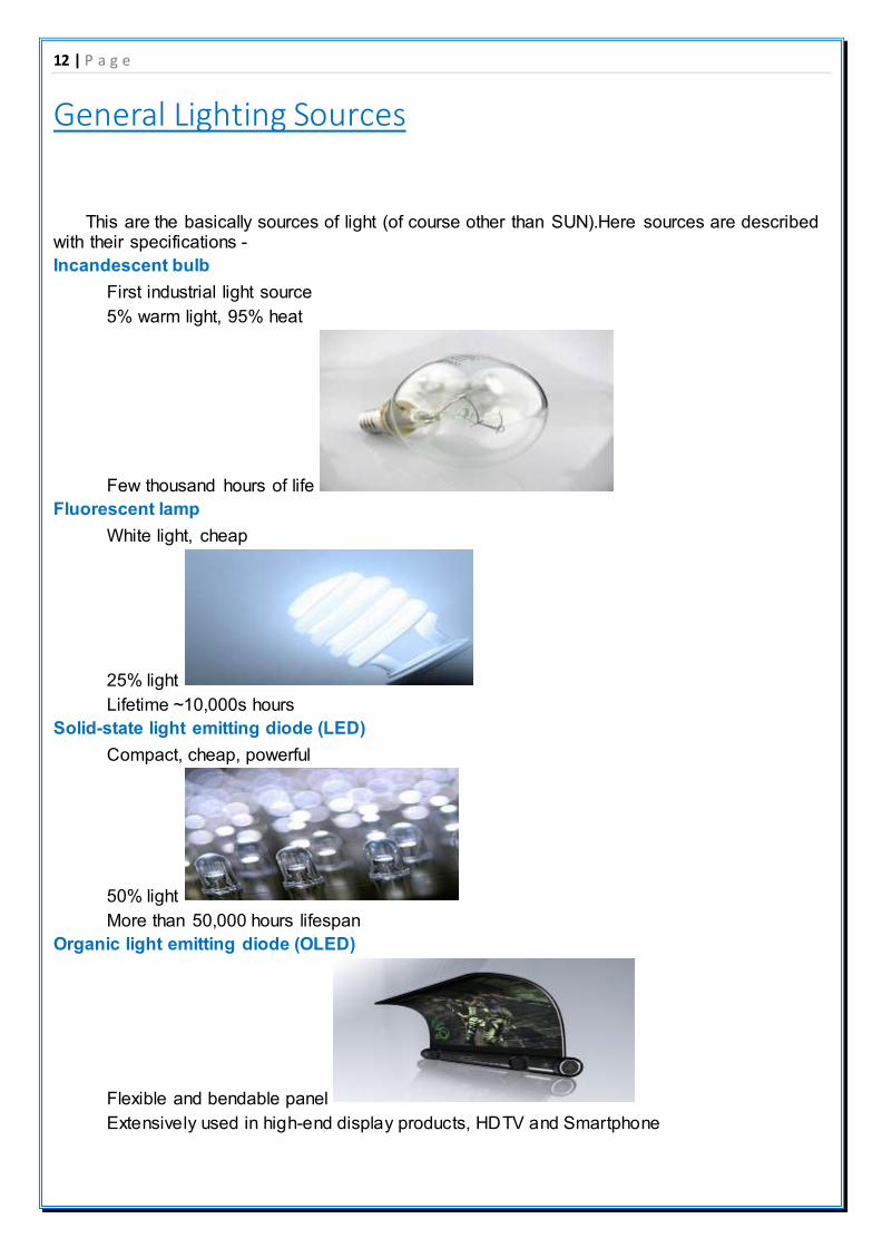
General Lighting Sources
This are the basically sources of light (of course other than SUN).Here sources are described with their specifications -
Incandescent bulb
First industrial light source
5% warm light, 95% heat
Few thousand hours of life
Fluorescent lamp
White light, cheap
25% light
Lifetime ~10,000s hours
Solid-state light emitting diode (LED)
Compact, cheap, powerful
50% light
More than 50,000 hours lifespan
Organic light emitting diode (OLED)
Flexible and bendable panel
Extensively used in high-end display products, HDTV and Smartphone
13 | P a g e
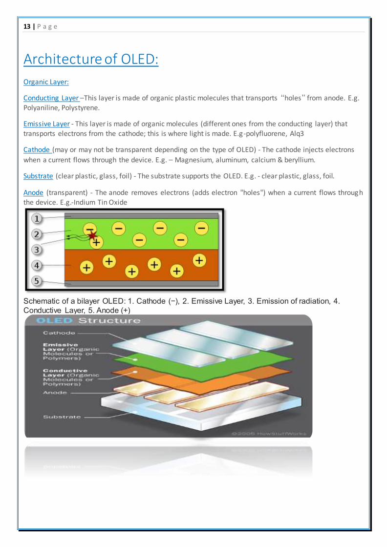
Architecture of OLED:
Organic Layer:
Conducting Layer –This layer is made of organic plastic molecules that transports “holes” from anode. E.g.
Polyaniline, Polystyrene.
Emissive Layer - This layer is made of organic molecules (different ones from the conducting layer) that transports electrons from the cathode; this is where light is made. E.g-polyfluorene, Alq3
Cathode (may or may not be transparent depending on the type of OLED) - The cathode injects electrons
when a current flows through the device. E.g. – Magnesium, aluminum, calcium & beryllium.
Substrate (clear plastic, glass, foil) - The substrate supports the OLED. E.g. - clear plastic, glass, foil.
Anode (transparent) - The anode removes electrons (adds electron "holes") when a current flows through the device. E.g.-Indium Tin Oxide
Schematic of a bilayer OLED: 1. Cathode (−), 2. Emissive Layer, 3. Emission of radiation, 4.
Conductive Layer, 5. Anode (+)
14 | P a g e
OLED Fabrication:
There are several process of OLED fabrication. Like-
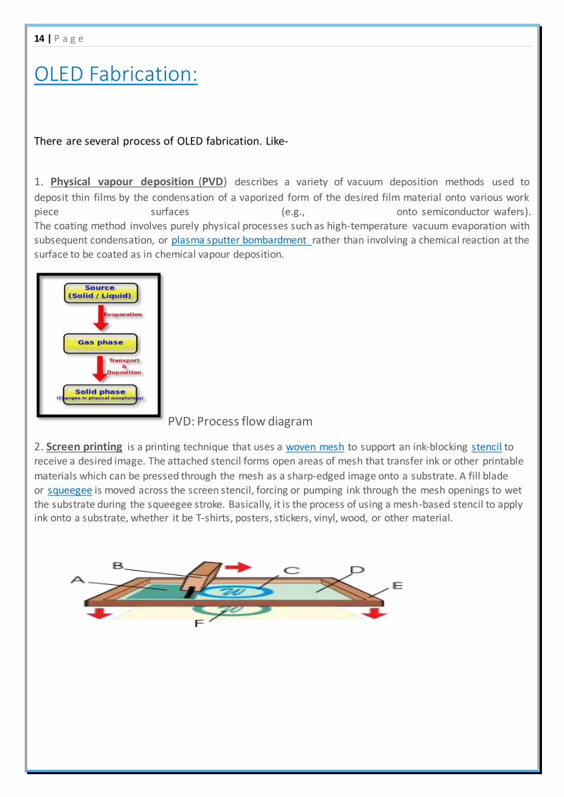
1. Physical vapour deposition (PVD) describes a variety of vacuum deposition methods used to
deposit thin films by the condensation of a vaporized form of the desired film material onto various work piece surfaces (e.g., onto semiconductor wafers).
The coating method involves purely physical processes such as high-temperature vacuum evaporation with subsequent condensation, or plasma sputter bombardment rather than involving a chemical reaction at the
surface to be coated as in chemical vapour deposition.
PVD: Process flow diagram
2. Screen printing is a printing technique that uses a woven mesh to support an ink-blocking stencil to receive a desired image. The attached stencil forms open areas of mesh that transfer ink or other printable
materials which can be pressed through the mesh as a sharp-edged image onto a substrate. A fill blade or squeegee is moved across the screen stencil, forcing or pumping ink through the mesh openings to wet
the substrate during the squeegee stroke. Basically, it is the process of using a mesh-based stencil to apply ink onto a substrate, whether it be T-shirts, posters, stickers, vinyl, wood, or other material.
15 | P a g e
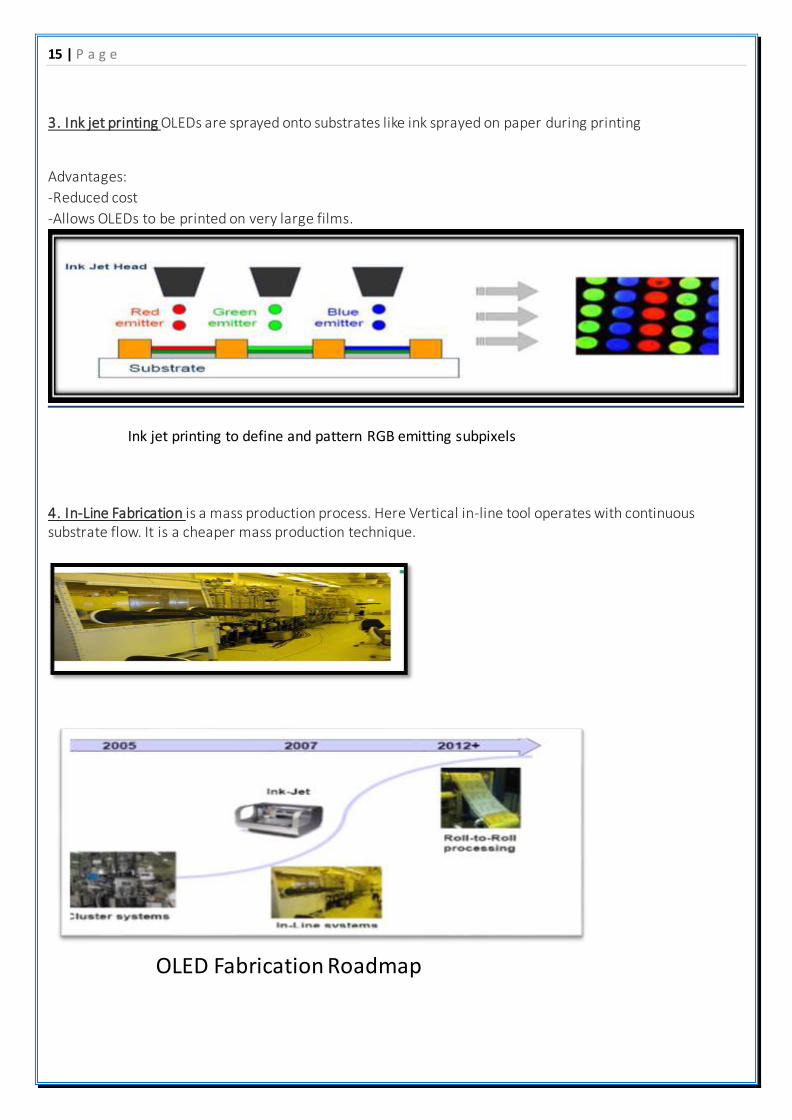
3. Ink jet printing OLEDs are sprayed onto substrates like ink sprayed on paper during printing
Advantages:
-Reduced cost
-Allows OLEDs to be printed on very large films.
Ink jet printing to define and pattern RGB emitting subpixels
4. In-Line Fabrication is a mass production process. Here Vertical in-line tool operates with continuous substrate flow. It is a cheaper mass production technique.
OLED Fabrication Roadmap
16 | P a g e
Working Principle: A typical OLED is composed of a layer of organic materials situated between two electrodes, the anode and
cathode, all deposited on a substrate. The organic molecules are electrically conductive as a result of
delocalization of pi electrons caused by conjugation over part or all of the molecule. These materials have
conductivity levels ranging from insulators to conductors, and are therefore considered organic
semiconductors. The highest occupied and lowest unoccupied molecular orbitals (HOMO and LUMO) of
organic semiconductors are analogous to the valence and conduction bands of inorganic semiconductors.
During operation, a voltage is applied across the OLED such that the anode is positive with respect to the cathode. Anodes are picked based upon the quality of their optical transparency, electrical conductivity, and chemical stability. A current of electrons flows through the device from cathode to anode, as electrons
are injected into the LUMO of the organic layer at the cathode and withdrawn from the HOMO at the anode. This latter process may also be described as the injection of electron holes into the HOMO.
Electrostatic forces bring the electrons and the holes towards each other and they recombine forming an ”exciton” a bound state of the electron and hole. This happens closer to the emissive layer, because in
organic semiconductors holes are generally more mobile than electrons. The decay of this excited state results in a relaxation of the energy levels of the electron, accompanied by emission
of radiation whose frequency is in the visible region. The frequency of this radiation depends on the band
gap of the material, in this case the difference in energy between the HOMO and LUMO.
Indium tin oxide (ITO) is commonly used as the anode material. It is transparent to visible light and has a
high work function which promotes injection of holes into the HOMO level of the or Experimental research
has proven that the properties of the anode, specifically the anode/hole transport layer (HTL) interface topography plays a major role in the efficiency, performance, and lifetime of organic light emitting diodes.
Imperfections in the surface of the anode decrease anode-organic film interface adhesion, increase electrical resistance, and allow for more frequent formation of non-emissive dark spots in the OLED
material adversely affecting lifetime. Mechanisms to decrease anode roughness for ITO/glass substrates include the use of thin films and self-assembled monolayers. Also, alternative substrates and anode
materials are being considered to increase OLED performance and li fetime. Possible examples include single crystal sapphire substrates treated with gold (Au) film anodes yielding lower work functions,
operating voltages, electrical resistance values, and increasing lifetime of OLEDs.
Single carrier devices are typically used to study the kinetics and charge transport mechanisms of an organic material and can be useful when trying to study energy transfer processes. As current through the
device is composed of only one type of charge carrier, either electrons or holes, recombination does not occur and no light is emitted. For example, electron only devices can be obtained by replacing ITO with a
lower work function metal which increases the energy barrier of hole injection. Similarly, hole only devices can be made by using a cathode made solely of aluminium, resulting in an energy barrier too large for
efficient electron injection.
17 | P a g e
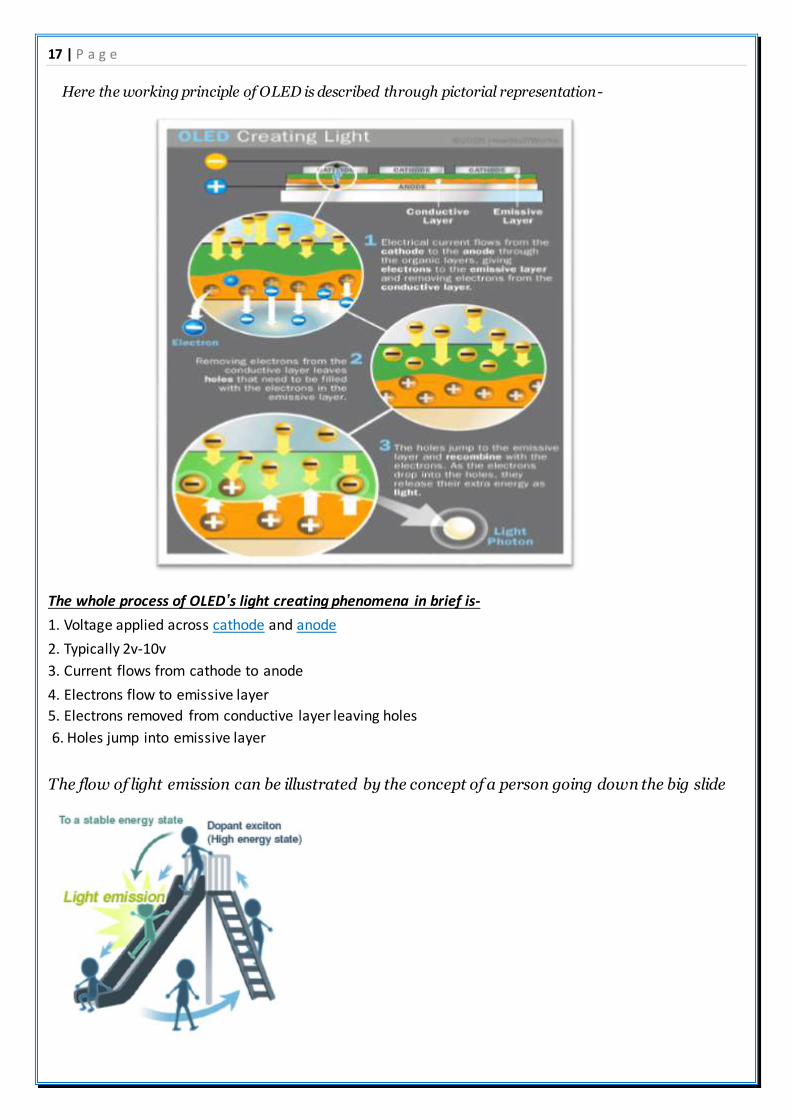
Here the working principle of OLED is described through pictorial representation-
The whole process of OLED’s light creating phenomena in brief is-
1. Voltage applied across cathode and anode
2. Typically 2v-10v
3. Current flows from cathode to anode
4. Electrons flow to emissive layer
5. Electrons removed from conductive layer leaving holes
6. Holes jump into emissive layer
The flow of light emission can be illustrated by the concept of a person going down the big slide
18 | P a g e
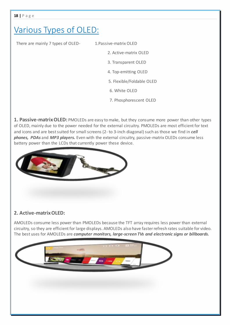
Various Types of OLED:
There are mainly 7 types of OLED- 1.Passive-matrix OLED
2. Active-matrix OLED
3. Transparent OLED
4. Top-emitting OLED
5. Flexible/Foldable OLED
6. White OLED
7. Phosphorescent OLED
1. Passive-matrix OLED: PMOLEDs are easy to make, but they consume more power than other types
of OLED, mainly due to the power needed for the external circuitry. PMOLEDs are most efficient for text
and icons and are best suited for small screens (2- to 3-inch diagonal) such as those we find in cell
phones, PDAs and MP3 players. Even with the external circuitry, passive-matrix OLEDs consume less battery power than the LCDs that currently power these device.
2. Active-matrix OLED:
AMOLEDs consume less power than PMOLEDs because the TFT array requires less power than external
circuitry, so they are efficient for large displays. AMOLEDs also have faster refresh rates suitable for video. The best uses for AMOLEDs are computer monitors, large-screen TVs and electronic signs or billboards.
19 | P a g e
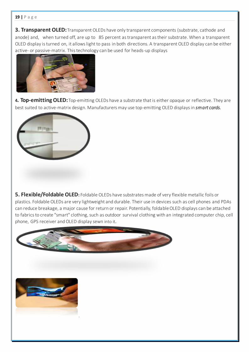
3. Transparent OLED: Transparent OLEDs have only transparent components (substrate, cathode and
anode) and, when turned off, are up to 85 percent as transparent as their substrate. When a transparent
OLED display is turned on, it allows light to pass in both directions. A transparent OLED display can be either
active- or passive-matrix. This technology can be used for heads-up displays
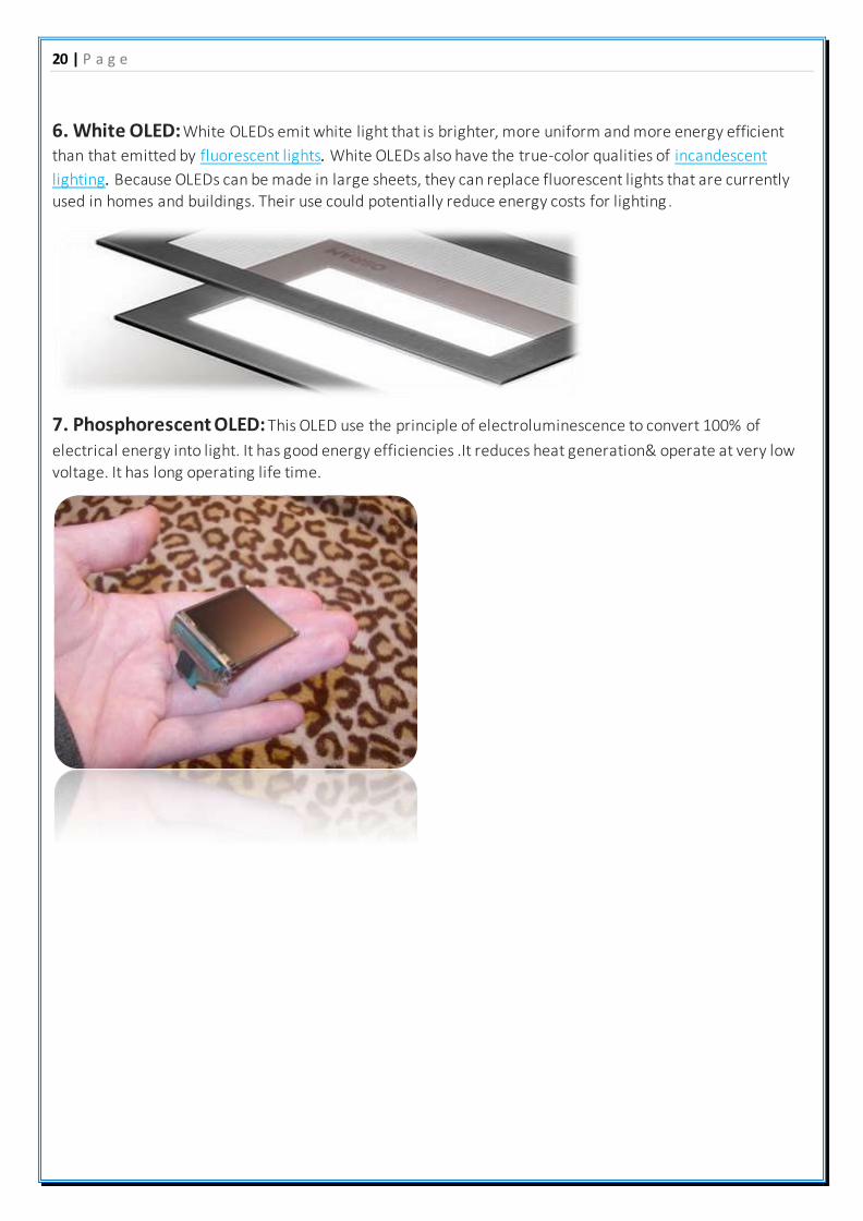
4. Top-emitting OLED: Top-emitting OLEDs have a substrate that is either opaque or reflective. They are
best suited to active-matrix design. Manufacturers may use top-emitting OLED displays in smart cards.
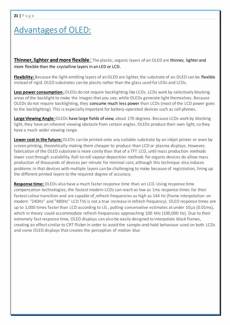
5. Flexible/Foldable OLED: Foldable OLEDs have substrates made of very flexible metallic foils or
plastics. Foldable OLEDs are very lightweight and durable. Their use in devices such as cell phones and PDAs
can reduce breakage, a major cause for return or repair. Potentially, foldable OLED displays can be attached
to fabrics to create "smart" clothing, such as outdoor survival clothing with an integrated computer chip, cell
phone, GPS receiver and OLED display sewn into it.
.
20 | P a g e
6. White OLED: White OLEDs emit white light that is brighter, more uniform and more energy efficient
than that emitted by fluorescent lights. White OLEDs also have the true-color qualities of incandescent
lighting. Because OLEDs can be made in large sheets, they can replace fluorescent lights that are currently used in homes and buildings. Their use could potentially reduce energy costs for lighting .
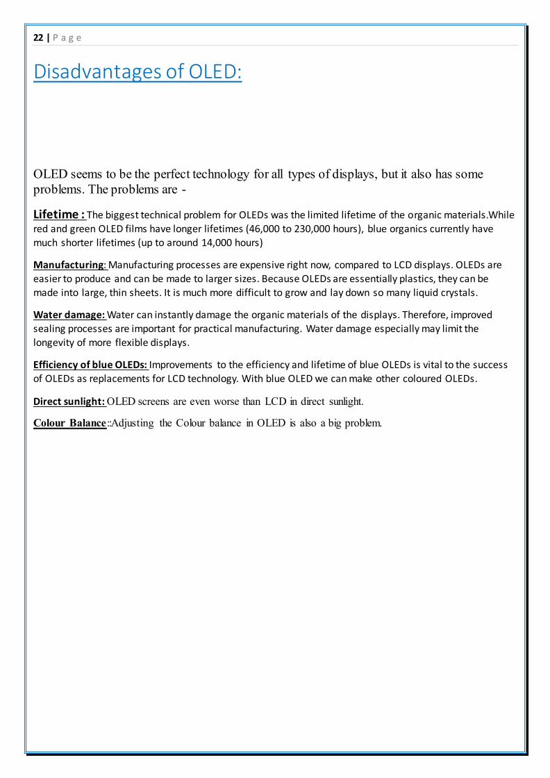
7. Phosphorescent OLED: This OLED use the principle of electroluminescence to convert 100% of
electrical energy into light. It has good energy efficiencies .It reduces heat generation& operate at very low
voltage. It has long operating life time.
21 | P a g e
Advantages of OLED:
Thinner, lighter and more flexible: The plastic, organic layers of an OLED are thinner, lighter and
more flexible than the crystalline layers in an LED or LCD.
Flexibility: Because the light-emitting layers of an OLED are lighter, the substrate of an OLED can be flexible instead of rigid. OLED substrates can be plastic rather than the glass used for LEDs and LCDs.
Less power consumption: OLEDs do not require backlighting like LCDs. LCDs work by selectively blocking areas of the backlight to make the images that you see, while OLEDs generate light themselves. Because OLEDs do not require backlighting, they consume much less power than LCDs (most of the LCD power goes to the backlighting). This is especially important for battery-operated devices such as cell phones.
Large Viewing Angle: OLEDs have large fields of view, about 170 degrees. Because LCDs work by blocking light, they have an inherent viewing obstacle from certain angles. OLEDs produce their own light, so they
have a much wider viewing range.
Lower cost in the future: OLEDs can be printed onto any suitable substrate by an inkjet printer or even by
screen printing, theoretically making them cheaper to produce than LCD or plasma displays. However,
fabrication of the OLED substrate is more costly than that of a TFT LCD, until mass production methods lower cost through scalability. Roll-to-roll vapour-deposition methods for organic devices do allow mass production of thousands of devices per minute for minimal cost, although this technique also induces
problems in that devices with multiple layers can be challenging to make because of registration, lining up the different printed layers to the required degree of accuracy.
Response time: OLEDs also have a much faster response time than an LCD. Using response time compensation technologies, the fastest modern LCDs can reach as low as 1ms response times for their
fastest colour transition and are capable of refresh frequencies as high as 144 Hz (frame interpolation on modern "240Hz" and "480Hz" LCD TVs is not a true increase in refresh frequency). OLED response times are
up to 1,000 times faster than LCD according to LG , putting conservative estimates at under 10μs (0.01ms),
which in theory could accommodate refresh frequencies approaching 100 kHz (100,000 Hz). Due to their extremely fast response time, OLED displays can also be easily designed to interpolate black frames,
creating an effect similar to CRT flicker in order to avoid the sample-and-hold behaviour used on both LCDs and some OLED displays that creates the perception of motion blur.
22 | P a g e
Disadvantages of OLED:
OLED seems to be the perfect technology for all types of displays, but it also has some
problems. The problems are -
Lifetime : The biggest technical problem for OLEDs was the limited lifetime of the organic materials.While
red and green OLED films have longer lifetimes (46,000 to 230,000 hours), blue organics currently have much shorter lifetimes (up to around 14,000 hours)
Manufacturing: Manufacturing processes are expensive right now, compared to LCD displays. OLEDs are
easier to produce and can be made to larger sizes. Because OLEDs are essentially plastics, they can be made into large, thin sheets. It is much more difficult to grow and lay down so many liquid crystals.
Water damage: Water can instantly damage the organic materials of the displays. Therefore, improved
sealing processes are important for practical manufacturing. Water damage especially may limit the
longevity of more flexible displays.
Efficiency of blue OLEDs: Improvements to the efficiency and lifetime of blue OLEDs is vital to the success
of OLEDs as replacements for LCD technology. With blue OLED we can make other coloured OLEDs.
Direct sunlight: OLED screens are even worse than LCD in direct sunlight.
Colour Balance::Adjusting the Colour balance in OLED is also a big problem.
23 | P a g e
Manufacturers & Commercial Uses:
OLED technology is used in commercial applications such as displays for mobile phones and portable digital
media players, car radios and digital cameras among others. Such portable applications favour the high
light output of OLEDs for readability in sunlight and their low power drain. Portable displays are also used intermittently, so the lower lifespan of organic displays is less of an issue. Prototypes have been made of
flexible and rollable displays which use OLEDs' unique characteristics. Applications in flexible signs and lighting are also and Novaledbeing developed. Philips Lighting have made OLED lighting samples under the
brand name "Lumiblade" available online in September, 2011.
Universal Display Corporation (UDC) is a leader in researching, developing and delivering OLED
technologies. Founded in 1994, the company currently owns or has exclusive, co-exclusive or sole license rights with respect to more than 3,000 issued and pending patents worldwide for the commercialization of
phosphorescent based OLEDs and also flexible, transparent and stacked OLEDs – for both display and lighting applications. Universal Display works and partners with a network of organizations,
including Princeton University, the University of Southern California, the University of Michigan, and PPG Industries, Inc. Its phosphorescent OLED technologies and materials are licensed and supplied to
companies such as Samsung, LG, AU Optronics CMEL, Pioneer, Panasonic Idemitsu OLED lighting
and Konica Minolta. UDC is working with many other companies, including Sony, DuPont and Novaled. Back in 2009 UDC claimed that "virtually all AMOLEDs on the market use our technology”.
OLEDs have been used in most Motorola and Samsung colour cell phones, as well as
some HTC, LG and Sony Ericsson models. Nokiahas also introduced some OLED products including
the N85 and the N86 8MP, both of which feature an AMOLED display. OLED technology can also be found
in digital media players such as the Creative ZEN V, the iriver clix, the Zune HD and the Sony Walkman X Series.
The Google and HTC Nexus One smartphone includes an AMOLED screen, as does HTC's
own Desire and Legend phones. However due to supply shortages of the Samsung-produced displays, certain HTC models will use Sony's SLCD displays in the future, while the Google and Samsung Nexus S
smartphone will use "Super Clear LCD" instead in some countries.
OLED displays were used in watches made by Fossil (JR-9465) and Diesel (DZ-7086).
Other manufacturers of OLED panels include Anwell Technologies Limited (Hong Kong), AU Optronics
(Taiwan), Chimei Innolux Corporation (Taiwan), LG (Korea), and others.
In 2009, Shearwater Research introduced the Predator as the first colour OLED diving computer available with a user replaceable battery.
24 | P a g e
DuPont stated in a press release in May 2010 that they can produce a 50-inch OLED TV in two minutes with a new printing technology. If this can be scaled up in terms of manufacturing, then the total cost of OLED TVs would be greatly reduced. DuPont also states that OLED TVs made with this less expensive technology can
last up to 15 years if left on for a normal eight hour day.
The use of OLEDs may be subject to patents held by Universal Display Corporation, Eastman
Kodak, DuPont, General Electric, Royal Philips Electronics, numerous universities and others. There are by now thousands of patents associated with OLEDs, both from larger corporations and smaller technology
companies. RIM, the maker of BlackBerry smartphones, use OLED displays in their BlackBerry 10 devices.
There is a relatively high failure rate when producing OLED screens. As little as a speck of dust can ruin a screen during production. Creating a battery that can be folded is another hurdle. However, Samsung have
accelerated their plans to release a foldable display by the end of 2015. Textiles incorporating OLEDs are an innovation in the fashion world and pose for a way to integrate lighting
to bring inert objects to a whole new level of fashion. The hope is to combine the comfort and low cost properties of textile with the OLEDs properties of illumination and low energy consumption. Although this
scenario of illuminated clothing is highly plausible, challenges are still a road block. Some issues include: the lifetime of the OLED, rigidness of flexible foil substrates, and the lack of research in making more fabric like photonic textiles
25 | P a g e
Conclusion: Organic Light Emitting Diodes are evolving as the next generation displays. It's truly going to be the future
of display.
Its flexibility & thickness gives a great opportunity for many applications in future’s smart phones, T.V
screens & in many other device displays.
As OLED display technology matures, it will be better able to improve upon certain existing limitations of LCD
including
High power consumption: OLED emits its own light & the
components of it are organic components .So, OLED consumes
much less power than LCDs.
Limited viewing angles: Unlike LCD, OLED do not have the
limitation in viewing angle. OLED screens can be viewed over 170
degree .So, using this property of OLED curved T.Vs are getting
made.
Poor contrast ratios: LCDs contrast ratio is 150,000:1, whereas
OLEDs contrast ratio is 100,000,000:1.So, we can see that OLED
gives a great viewing experience compared to LCD.
So, that day is not so far when OLED will replace current million dollar LED and LCD technologies.Iintegrated touch OLED display will be potential competitive item too.
Organic light emitting diode is also an environment friendly technology. It pollutes the environment less compare to the other technologies available in market till date. It's made of organic compounds & sometimes plastics are used to prepare the displays, so its pollution effect is not too much dangerous too. So, OLED is a good candidate of green solution for display
But the research work on OLED is still going on. So, market price of it is pretty high nowadays .Perhaps with
more progress in the research work, someday less expensive OLEDs will be available in the market.
The technology of flexibility & ultra-thickness are increasing day by day. Probably in near future mobile screens will be thin like a blade.
26 | P a g e
Recommendation:
Organic Light Emitting Diode has a huge potential. It can be the answer to all display related future
technologies.
Research on OLED is going on worldwide. In near future we may able to see- Curved OLED displays, placed on non-flat surfaces
Wearable OLEDs
Transparent OLEDs embedded in windows: lighting defining new ways to light a space
New designs for lamps
And many more we cannot even imagine standing on today’s morning...
Usage of OLED can be seen in today’s cars. Dashboard displays
Windshield transparent OLEDs
Internal lighting
External lighting
Back-window alerts and messaging (as seen on the EDAG prototype)
Data glass: Google made a google glass, which can be future’s instant Wikipedia. OLED can be used in GPS
system. Which can give a new dimension to navigation system. Nokia concept OLED scroll Laptop. Samsung is also developing a piece of paper which can be used like a newspaper. This digital OLED
newspaper has a touchscreen and you can surf through the content .SMD expect to commercialize this product in 2015.
But we have to manufacturer OLED focusing on finding a cheap way to produce & "Roll-to-Roll"
Manufacturing. We have to focus on increasing efficiency of blue luminance because to make other coloured screens. Boosting overall lifespan also very needed.
27 | P a g e
References:
1. Beardsley, James. "International OLED Technology Roadmap." IEEE JOURNAL OF SELECTED TOPICS IN
QUANTUM ELECTRONICS. Jan. 2004. IEEE. <http://ieeexplore.ieee.org/stamp/stamp.jsp?arnumber=01288066>.
2. Freudenrich, Craig, Ph.D. "How OLEDs Work”. Howstuffworks. 2008.
<http://electronics.howstuffworks.com/oled.htm>.
3. "OLED Lights and Sony OLEDs." OLED displays and television resources, info and news 2015. <http://www.oled-info.com/>.
4. http://en.wikipedia.org/wiki/OLED
5. "Philips Lumiblade". Lumiblade.com. 2009-08-09. Retrieved 2009-08-17.
6. Session Border Controller. Tmcnet.com (2011-09-13). Retrieved 2012-11-12.
7. http://www.oled-info.com/universal_display_udc
8. Electronic News, OLEDs Replacing LCDs in Mobile Phones, April 7, 2005. Retrieved July 28, 2007.
9."HTC ditches Samsung AMOLED display for Sony's Super LCDs". International Business Times. 2010-07-
26. Retrieved 2010-07-30.
10."Google Nexus S to feature Super Clear LCD in Russia (and likely in other countries, too)".
UnwiredView.com. 2010-12-07. Retrieved 2010-12-08
11. http://www.oled-info.com/samsung-accelerate-flexible-oled-development
12. "OLED TV estimated lifespan shorter than expected". HDTV Info Europe. Hdtvinfo.eu (2008-05-08).
13."OLED lifespan doubled?" HDTV Info Europe. Hdtvinfo.eu (2008-01-25).
14. Kim, Seoul Ong; Lee, Kuma He; Kim, GU Young; Seo, Ji Hoon; Kim, Young Kwan; Yoon, Seung Soo (2010). "A highly efficient deep blue fluorescent OLED based on diphenylaminofluorenylstyrene-containing
emitting materials". Synthetic Metals 160 (11–12): 1259.
15. https://www.youtube.com/watch?v=CAgRF8TibJ0
16. https://www.youtube.com/watch?v=mLMWXBv5rY4
28 | P a g e
Glossary:
Pixel A pixel
(or picture element) is the smallest item of information in an image
Electroluminescence (EL) is an optical phenomenon and electrical phenomenon in which a material emits
light in response to an electric current passed through it, or to a strong electric field.
Organic compound an organic compound is any member of a large class of chemical
compounds whose molecules contain carbon.
SMD Samsung Mobile Display
Plasma sputter bombardment a process whereby atoms are ejected from a solid target material due to
bombardment of the target by energetic particles
Stencil produces an image or pattern by applying pigment to a surface over an intermediate object with
designed gaps in it which create the pattern or image by only allowing the pigment to reach some parts of the surface
Squeegee a tool with a flat, smooth rubber blade, used to remove or control the flow of liquid on a flat
surface. It is used for cleaning and in printing.
Exciton a bound state of an electron and an electron whole which are attracted to each other by the
electrostatic Coulomb force.
Adhesion the tendency of dissimilar particles or surfaces to cling to one another.
ITO tin-doped indium oxide a solid solution of indium oxide (In2O3) and tin (IV) oxide (SnO2), typically 90%
In2O3, 10% SnO2 by weight. It is transparent and colourless in thin layers while in bulk form it is yellowish to
grey. In the infrared region of the spectrum it acts as a metal-like mirror.
Cathode the electrode from which a conventional current leaves a polarized electrical device.
Anode an electrode through which electric current flows into a polarized electrical device.
Incandescent light bulb is an electric light which produces light with a wire filament heated to a high
temperature by an electric current passing through it, until it glows
Fluorescent lights a low pressure mercury-vapour gas-discharge lamp that uses fluorescence to produce
visible light. An electric current in the gas excites mercury vapour which produces short-
wave ultraviolet light that then causes a phosphor coating on the inside of the bulb to glow.

![COLOR-TUNABLE OF ORGANIC LIGHT EMITTING DIODE MEH … · organic solar cell and light emission in organic light emitting diode, the responsible of theses process is π-electrons [7].The](https://img.pdfslide.us/doc/110x75/60227064e9a86266f43e46d9/color-tunable-of-organic-light-emitting-diode-meh-organic-solar-cell-and-light-emission.jpg)