Embed Size (px)
Citation preview
Studying the change in organic light-emitting diode performanceat various vacuum-deposition rates of hole and electron transportlayers
AMIR MIKAEILI and EZEDDIN MOHAJERANI*
Laser and Plasma Research Institute, Shahid Beheshti University, Tehran 1983963113, Iran
*Author for correspondence ([email protected])
MS received 4 December 2019; accepted 29 June 2020
Abstract. The electroluminescence (EL) of classic and thermally activated delayed fluorescence (TADF) organic light-
emitting diodes (OLEDs) at various vacuum-deposition rates of hole and electron transport layer (HTL and ETL) has been
studied. The external quantum efficiency (EQE) measurements showed that the best performance devices were those with
a high charge carrier balance inside the emitting layer, which was engineered using hole and electron current manipulation
as a result of vacuum-deposition rate control. Changing the vacuum-deposition rate of HTL and ETL leads to a change in
the maximum EQE (EQEmax) of the classic and TADF OLEDs without obvious changes in EQE roll-off ratio at high
current density. We used a simple analytical model to clarify that the enhanced hole current in HTL at high deposition
rates is dominated by high hole mobility attributed to the increased hole hopping rate due to the reduction of the
intermolecular separation between horizontally oriented N,N0-diphenyl-N,N0-bis(1-naphthyl)-1,10-biphenyl-4,40-diamine
(a-NPD) molecules. The increase in the electron current of tris-(8-hydroxyquinoline) aluminium (Alq3) ETL at low
deposition rate was ascribed to high electron injection from cathode into ETL by the fabrication and comparison of
J–V characteristic of two electron-only devices with a difference at deposition rate of ETL near cathode interface. Finally,
we introduced an OLED with novel gradient and barrier structures for the emitting layer in which high injected charge
carriers recombined inside added recombination zone to raise radiative recombination and efficiency of the device. Our
results demonstrated that EL efficiency of an OLED can be changed by controlling the vacuum-deposition rate of organic
layers.
Keywords. Novel gradient and barrier structures; controlling the vacuum-deposition rate; electroluminescence (EL)
efficiency; charge hopping rate; charge recombination zone.
1. Introduction
Besides the unique properties of organic semiconductors,
such as ability of determining chemical structure manipu-
lation, the potential for simplicity and safety in flexible thin
film fabrication as well as low-cost processes, small mole-
cule organic semiconductors, have provided a novel
exclusive feature of manipulation of a layer structure during
the vacuum-deposition process [1–10]. Charge hopping rate
inside the layer and charge injection at the organic/organic
and organic/metal interface can, in principle, be affected
markedly as a result of changes in electrical performance of
the layer [9–18].
Control of molecular arrangement and structure of layers
during vacuum-deposition, which is an obvious merit of this
thin film making process as opposed to others such as
solution-based methods, is of intense interest [8,9,18–21].
The structural and electrical characteristics of the layer can
be engineered. The understanding of physical mechanisms
related to charge carrier transport and injection through an
organic layer can be developed as well.
Despite comprehensive research on the effect of vacuum-
deposition rate on organic layer characteristics which have
been done during the last decade, attempts to comprehend
the mechanisms governing on charge transport and injection
seem to be insufficient [8,9,18–21]. Recently, the key role
of molecular orientation in electrical performance of N,N0-diphenyl-N,N0-bis(1-naphthyl)-1,10-biphenyl-4,40-diamine
(a-NPD) thin films vacuum-deposited at various deposition
rates has been demonstrated [22]. The a-NPD molecules
were horizontally oriented relative to the substrate plane at
high deposition rate which resulted in increasing the hole
current. However, the mechanism of improving hole
transport inside the layer was unclear. Regarding the
Electronic supplementary material: The online version of this article (https://doi.org/10.1007/s12034-020-02189-1) contains supple-
mentary material, which is available to authorized users.
Bull Mater Sci (2020) 43:229 � Indian Academy of Scienceshttps://doi.org/10.1007/s12034-020-02189-1Sadhana(0123456789().,-volV)FT3](0123456789().,-volV)
electrons, tris-(8-hydroxyquinoline) aluminium (Alq3) as an
electron transport layer (ETL) showed higher electron cur-
rent at lower deposition rates, which was attributed to the
reduced surface roughness at the Alq3/cathode interface
[22]. We speculated that smooth interface between Alq3layer and cathode facilitates electron injection.
Also, there have been several papers endeavouring to
clarify the organic light-emitting diode (OLED) perfor-
mance at various organic layer(s) deposition rates by
studying the changes in OLED characteristics [8,9,18–20].
Besides the charge carrier injection from electrodes to
organic layers and charge carrier transport through organic
layers towards emitting layer, the vacuum-deposition rate of
emitting layer can affect charge carrier recombination zone,
exciton production and annihilation, suppression of effi-
ciency roll-off at high current densities, which are of intense
interested parameters, particularly with regard to thermally
activated delayed fluorescence (TADF) OLEDs [23–30].
Indeed, general comprehension of physical processes and
performance of OLEDs with different structures associated
with organic layer(s) vacuum-deposition rate still needs to
be rendered.
In this study, a classic structure OLED with Alq3 as a
classic fluorescent emitting layer and a TADF OLED
structure were considered for evaluating their electrolumi-
nescent characteristics at various vacuum-deposition rates
of charge carrier transport and emitting layers. Due to the
decomposition of TADF emitters at high vacuum-deposi-
tion rates, the effect of emitting layer deposition rate on
OLED performance was studied only in the classic struc-
ture. Moreover, evaluating the TADF OLED performance at
various deposition rates can be of intense interest. Next, our
study focused on the electrical properties of organic layers
at different vacuum-deposition rates to comprehend the
physical mechanisms of changes in hole and electron
injection, transport and recombination. Regarding the a-NPD hole transport layer (HTL), we tried to simulate the
effect of molecular orientation on hole hopping rate by
using non-adiabatic Marcus–Hush theory for the inter-
molecular hole transfer rate and a simple geometrical
model. Also, we demonstrated the facilitation of electron
injection from cathode to the Alq3 ETL by depositing a thin
smooth Alq3 layer at the interface of Alq3/cathode. Finally,
we used these findings to introduce new structures for
emitting layer in which we made an additional recombi-
nation zone in order to produce more excitons and increase
the efficiency of OLED.
2. Experimental
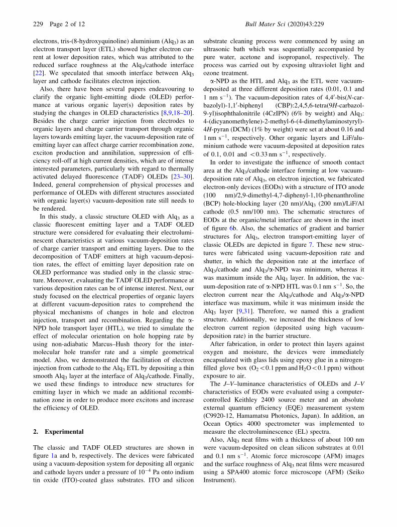
The classic and TADF OLED structures are shown in
figure 1a and b, respectively. The devices were fabricated
using a vacuum-deposition system for depositing all organic
and cathode layers under a pressure of 10�4 Pa onto indium
tin oxide (ITO)-coated glass substrates. ITO and silicon
substrate cleaning process were commenced by using an
ultrasonic bath which was sequentially accompanied by
pure water, acetone and isopropanol, respectively. The
process was carried out by exposing ultraviolet light and
ozone treatment.
a-NPD as the HTL and Alq3 as the ETL were vacuum-
deposited at three different deposition rates (0.01, 0.1 and
1 nm s�1). The vacuum-deposition rates of 4,40-bis(N-car-bazolyl)-1,10-biphenyl (CBP):2,4,5,6-tetra(9H-carbazol-
9-yl)isophthalonitrile (4CzIPN) (6% by weight) and Alq3:
4-(dicyanomethylene)-2-methyl-6-(4-dimethylaminostyryl)-
4H-pyran (DCM) (1% by weight) were set at about 0:16 and
1 nm s�1, respectively. Other organic layers and LiF/alu-
minium cathode were vacuum-deposited at deposition rates
of 0.1, 0.01 and \0:33 nm s�1, respectively.
In order to investigate the influence of smooth contact
area at the Alq3/cathode interface forming at low vacuum-
deposition rate of Alq3, on electron injection, we fabricated
electron-only devices (EODs) with a structure of ITO anode
(100 nm)/2,9-dimethyl-4,7-diphenyl-1,10-phenanthroline
(BCP) hole-blocking layer (20 nm)/Alq3 (200 nm)/LiF/Al
cathode (0.5 nm/100 nm). The schematic structures of
EODs at the organic/metal interface are shown in the inset
of figure 6b. Also, the schematics of gradient and barrier
structures for Alq3, electron transport-emitting layer of
classic OLEDs are depicted in figure 7. These new struc-
tures were fabricated using vacuum-deposition rate and
shutter, in which the deposition rate at the interface of
Alq3/cathode and Alq3/a-NPD was minimum, whereas it
was maximum inside the Alq3 layer. In addition, the vac-
uum-deposition rate of a-NPD HTL was 0:1 nm s�1. So, the
electron current near the Alq3/cathode and Alq3/a-NPDinterface was maximum, while it was minimum inside the
Alq3 layer [9,31]. Therefore, we named this a gradient
structure. Additionally, we increased the thickness of low
electron current region (deposited using high vacuum-
deposition rate) in the barrier structure.
After fabrication, in order to protect thin layers against
oxygen and moisture, the devices were immediately
encapsulated with glass lids using epoxy glue in a nitrogen-
filled glove box (O2\0:1 ppm andH2O\0:1 ppm) without
exposure to air.
The J–V–luminance characteristics of OLEDs and J–V
characteristics of EODs were evaluated using a computer-
controlled Keithley 2400 source meter and an absolute
external quantum efficiency (EQE) measurement system
(C9920-12, Hamamatsu Photonics, Japan). In addition, an
Ocean Optics 4000 spectrometer was implemented to
measure the electroluminescence (EL) spectra.
Also, Alq3 neat films with a thickness of about 100 nm
were vacuum-deposited on clean silicon substrates at 0.01
and 0.1 nm s�1. Atomic force microscope (AFM) images
and the surface roughness of Alq3 neat films were measured
using a SPA400 atomic force microscope (AFM) (Seiko
Instrument).
229 Page 2 of 12 Bull Mater Sci (2020) 43:229
3. Results and discussion
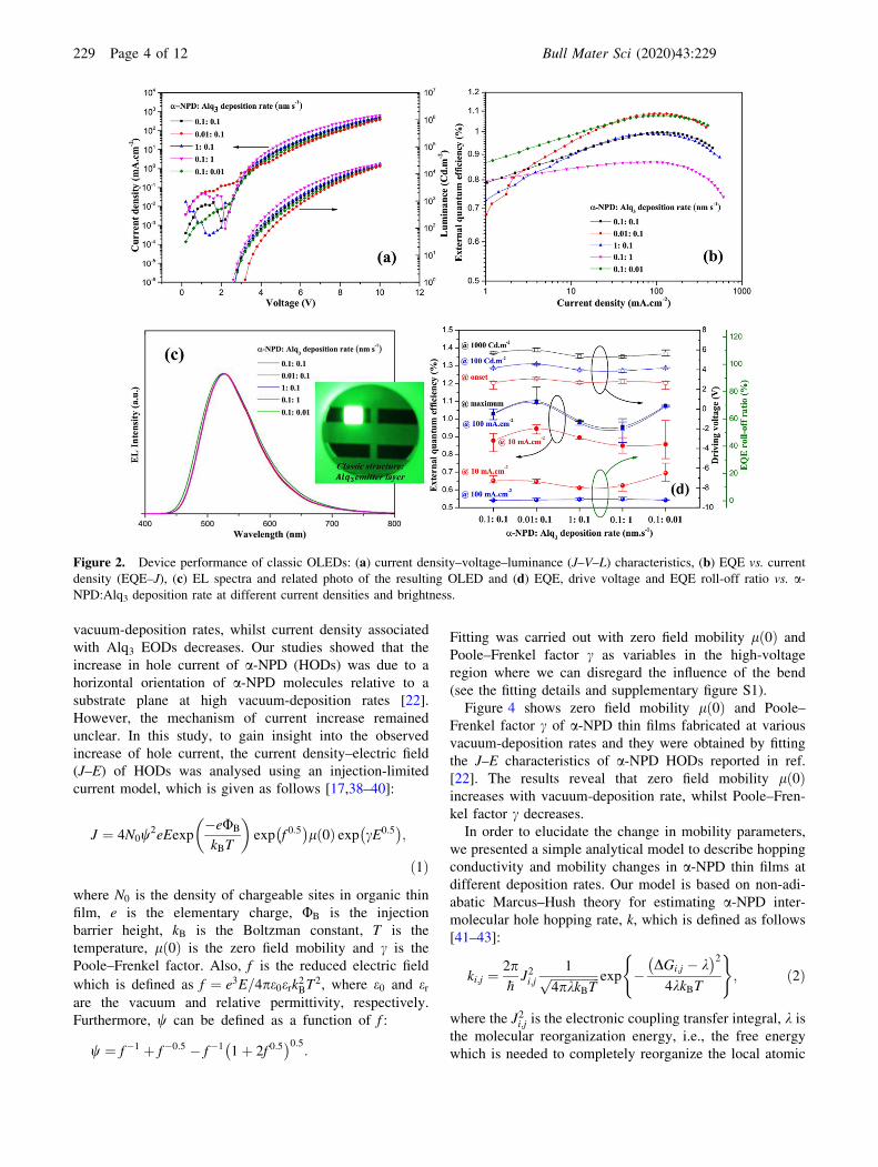
3.1 Classic and TADF OLED performances
The detailed classic and TADF OLED performances are
depicted in figures 2 and 3 and tables 1 and 2, respectively.
The hole–electron recombination zone and emitting region of
the classic structure are pinned near the interface of a-NPD(HTL) and Alq3 (ETL-EL) due to low hole and electron
mobility in ETL and HTL, respectively [9,32,33], whereas in
the TADF structure, 10 nmT2T blocks holes to penetrate into
Alq3 layer and recombination zone is inside the CBP:4CzIPN
layer. Regarding classic OLEDs, the structures in which
a-NPD (HTL) and Alq3 (ETL-EL) vacuum-deposition rates
were 0.01:0.1 nm s�1 and 0.1:0.01 nm s�1 had the best
performance (EQEmax = 1.09 and 1.08%, respectively). The
change in EQE of OLED can be originated from the change
in: I – the light out-coupling efficiency (gout), II – the chargebalance factor (ge�h), III – the singlet and triplet exciton
generation efficiency (gexciton) and IV – the photolumines-
cence (PL) quantum yield (gPL), according to equation
EQE ¼ gout � ge�h � gexciton � gPL [9,34,35]. The observed
changes in EQE of OLEDs at different vacuum-deposition
rates of HTL, ETL and EL are assumed to be independent of
light out-coupling factor, exciton generation efficiency and
PL quantum yield [9]. However, it is demonstrated that
organic layer characteristics can be changed at various vac-
uum-deposition rates resulting in charge carrier mobility
changes [9,15,31]. Concerning a-NPD, hole mobility
increases at high vacuum-deposition rates [9]. Recently, we
showed that the increase in hole mobility of a-NPD layer at
high deposition rate can be attributed to horizontally oriented
molecules. Furthermore, reduced surface roughness of Alq3
layer can facilitate electron injection from cathode and cau-
ses high electron current [22]. Also, in the classic structure
OLED at equal a-NPD:Alq3 deposition rate (0.1:0.1 nm s�1),
the hole is the majority carrier [36,37]. So, in this condition
charge carrier imbalance could reduce EQE. Accordingly,
the increase in EQE at a-NPD:Alq3 vacuum-deposition rates
of 0.01:0.1 nm s�1 and 0.1:0.01 nm s�1 can be raised from
higher charge carrier balance at the recombination zone.
Moreover, EL peak remained unchanged at different vac-
uum-deposition rates because of no change in recombination
zone position. Also, there was no meaningful change in EQE
roll-off ratio at various HTL, ETL and EL deposition rates.
Similarly, TADF OLEDs with a-NPD as hole-transport
and Alq3 as electron transport layers fabricated at vacuum-
deposition rates of 0.01:0.1 and 0.1:0.01 nm s�1, respec-
tively, showed the best efficiencies (EQE = 11.5 and 12.0%
at 10 mA cm�2 and EQE = 7.1 and 7.1% at 100 mA cm�2).
Additionally, the latter showed the best maximum EQE.
Interestingly, it seemed that HTL and effect on ETL
vacuum-deposition rate has no effect on the EL peak;
however, as it can be seen from figure 3d, the EQE roll-off
ratio was the minimum for the mentioned structures.
Although the change in the EQE of OLEDs was small,
especially concerning TADF OLEDs probably because of
the unchanged vacuum-deposition rate of the emitting layer,
it will increase noticeably by using novel gradient and
barrier structures as we will show later.
3.2 Origin of charge carrier mobility changes
Recently, we have demonstrated that current density of
a-NPD hole-only devices (HODs) increases at high
Figure 1. Schematic structure of (a) classic and (b) TADF OLEDs and energy diagrams of organic layers.
Bull Mater Sci (2020) 43:229 Page 3 of 12 229
vacuum-deposition rates, whilst current density associated
with Alq3 EODs decreases. Our studies showed that the
increase in hole current of a-NPD (HODs) was due to a
horizontal orientation of a-NPD molecules relative to a
substrate plane at high vacuum-deposition rates [22].
However, the mechanism of current increase remained
unclear. In this study, to gain insight into the observed
increase of hole current, the current density–electric field
(J–E) of HODs was analysed using an injection-limited
current model, which is given as follows [17,38–40]:
J ¼ 4N0w2eEexp
�eUB
kBT
� �exp f 0:5
� �l 0ð Þ exp cE0:5
� �;
ð1Þ
where N0 is the density of chargeable sites in organic thin
film, e is the elementary charge, UB is the injection
barrier height, kB is the Boltzman constant, T is the
temperature, l 0ð Þ is the zero field mobility and c is the
Poole–Frenkel factor. Also, f is the reduced electric field
which is defined as f ¼ e3E=4pe0erk2BT2, where e0 and er
are the vacuum and relative permittivity, respectively.
Furthermore, w can be defined as a function of f :
w ¼ f�1 þ f�0:5 � f�1 1þ 2f 0:5� �0:5
:
Fitting was carried out with zero field mobility l 0ð Þ and
Poole–Frenkel factor c as variables in the high-voltage
region where we can disregard the influence of the bend
(see the fitting details and supplementary figure S1).
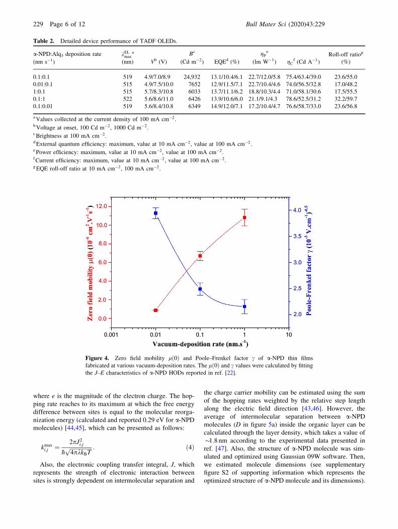
Figure 4 shows zero field mobility l 0ð Þ and Poole–
Frenkel factor c of a-NPD thin films fabricated at various
vacuum-deposition rates and they were obtained by fitting
the J–E characteristics of a-NPD HODs reported in ref.
[22]. The results reveal that zero field mobility l 0ð Þincreases with vacuum-deposition rate, whilst Poole–Fren-
kel factor c decreases.
In order to elucidate the change in mobility parameters,
we presented a simple analytical model to describe hopping
conductivity and mobility changes in a-NPD thin films at
different deposition rates. Our model is based on non-adi-
abatic Marcus–Hush theory for estimating a-NPD inter-
molecular hole hopping rate, k, which is defined as follows
[41–43]:
ki;j ¼2p�hJ2i;j
1ffiffiffiffiffiffiffiffiffiffiffiffiffiffiffiffi4pkkBT
p exp �DGi;j � k� �2
4kkBT
( ); ð2Þ
where the J2i;j is the electronic coupling transfer integral, k is
the molecular reorganization energy, i.e., the free energy
which is needed to completely reorganize the local atomic
Figure 2. Device performance of classic OLEDs: (a) current density–voltage–luminance (J–V–L) characteristics, (b) EQE vs. current
density (EQE–J), (c) EL spectra and related photo of the resulting OLED and (d) EQE, drive voltage and EQE roll-off ratio vs. a-NPD:Alq3 deposition rate at different current densities and brightness.
229 Page 4 of 12 Bull Mater Sci (2020) 43:229
reorganization of one state to the another state without
charge transfer which is equal to half the polaron binding
energy, kB is the Boltzmann’s constant, T is the tempera-
ture, and DGi;j is the difference of free energy between the
initial and final sites.
For two sites with a separation distance, Dri;j, inside the
applied electric field, E, the free energy difference between
them is given by [43]
DGi;j ¼ eDri;j � E; ð3Þ
Figure 3. Device performance of TADF OLEDs: (a) current density–voltage–luminance (J–V–L) characteristics, (b) EQE vs. current
density (EQE–J), (c) EL spectra and related photo of the resulting OLED and (d) EQE, drive voltage and EQE roll-off ratio vs. a-NPD:Alq3 deposition rate at different current densities and brightness.
Table 1. Detailed device performance of classic OLEDs.
a-NPD:Alq3 deposition rate
(nm s�1)
kELmaxa
(nm) Vb (V)
Bc
(Cd m�2) EQEd (%) gPe (lm W�1) gC
f (Cd A�1)
Roll-off ratiog
(%)
0.1:0.1 523 2.9/3.9/5.5 4691 0.94/0.87/0.94 2.35/1.73/1.29 4.80/4.25/4.71 11.2/2.1
0.01:0.1 527 3.2/4.5/6.2 5507 1.09/0.96/1.08 1.79/1.68/1.31 5.56/4.87/5.52 11.8/1.0
1:0.1 527 2.7/3.9/5.6 5249 0.99/0.89/0.98 2.50/1.79/1.31 5.01/4.56/4.96 11.0/2.0
0.1:1 527 2.6/3.7/5.2 4347 0.87/0.85/0.86 2.60/1.77/1.25 4.35/4.14/4.27 5.7/2.3
0.1:0.01 527 2.8/4.1/6.0 5792 1.08/1.08/1.09 2.47/1.71/1.34 5.61/4.71/5.51 17.1/1.8
aValues collected at the current density of 100 mA cm�2.bVoltage at onset, 100 Cd m�2, 1000 Cd m�2.cBrightness at 100 mA cm�2.dExternal quantum efficiency: maximum, value at 10 mA cm�2, value at 100 mA cm�2.ePower efficiency: maximum, value at 10 mA cm�2, value at 100 mA cm�2.fCurrent efficiency: maximum, value at 10 mA cm�2, value at 100 mA cm�2.gEQE roll-off ratio at 10 mA cm�2, 100 mA cm�2.
Bull Mater Sci (2020) 43:229 Page 5 of 12 229
where e is the magnitude of the electron charge. The hop-
ping rate reaches to its maximum at which the free energy
difference between sites is equal to the molecular reorga-
nization energy (calculated and reported 0.29 eV for a-NPDmolecules) [44,45], which can be presented as follows:
kmaxi;j ¼
2pJ2i;j�h
ffiffiffiffiffiffiffiffiffiffiffiffiffiffiffiffi4pkkBT
p : ð4Þ
Also, the electronic coupling transfer integral, J, which
represents the strength of electronic interaction between
sites is strongly dependent on intermolecular separation and
the charge carrier mobility can be estimated using the sum
of the hopping rates weighted by the relative step length
along the electric field direction [43,46]. However, the
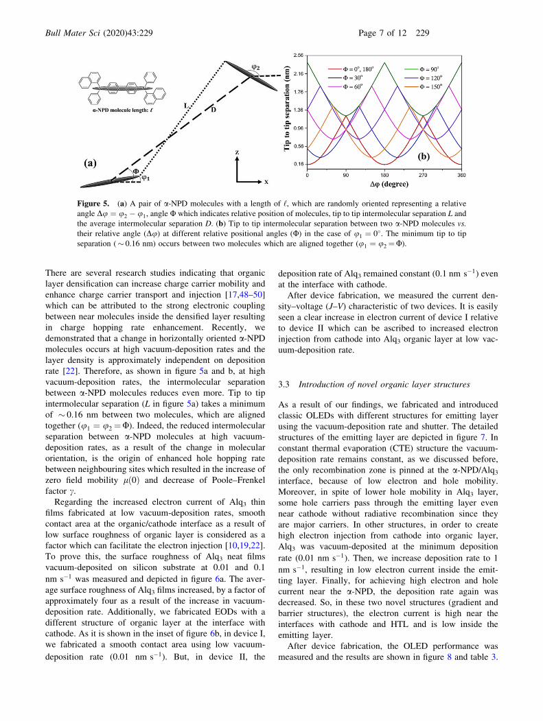
average of intermolecular separation between a-NPDmolecules (D in figure 5a) inside the organic layer can be
calculated through the layer density, which takes a value of
�1:8 nm according to the experimental data presented in
ref. [47]. Also, the structure of a-NPD molecule was sim-
ulated and optimized using Gaussian 09W software. Then,
we estimated molecule dimensions (see supplementary
figure S2 of supporting information which represents the
optimized structure of a-NPD molecule and its dimensions).
Table 2. Detailed device performance of TADF OLEDs.
a-NPD:Alq3 deposition rate
(nm s�1)
kELmaxa
(nm) Vb (V)
Bc
(Cd m�2) EQEd (%)
gPe
(lm W�1) gCf (Cd A�1)
Roll-off ratiog
(%)
0.1:0.1 519 4.9/7.0/8.9 24,932 13.1/10.4/6.1 22.7/12.0/5.8 75.4/63.4/39.0 23.6/55.0
0.01:0.1 515 4.9/7.5/10.0 7652 12.9/11.5/7.1 22.7/10.4/4.6 74.0/56.5/32.8 17.0/48.2
1:0.1 515 5.7/8.3/10.8 6033 13.7/11.1/6.2 18.8/10.3/4.4 71.0/58.1/30.6 17.5/55.5
0.1:1 522 5.6/8.6/11.0 6426 13.9/10.6/6.0 21.1/9.1/4.3 78.6/52.5/31.2 32.2/59.7
0.1:0.01 519 5.6/8.4/10.8 6349 14.9/12.0/7.1 17.2/10.4/4.7 76.6/58.7/33.0 23.6/56.8
aValues collected at the current density of 100 mA cm�2.bVoltage at onset, 100 Cd m�2, 1000 Cd m�2.cBrightness at 100 mA cm�2.dExternal quantum efficiency: maximum, value at 10 mA cm�2, value at 100 mA cm�2.ePower efficiency: maximum, value at 10 mA cm�2, value at 100 mA cm�2.fCurrent efficiency: maximum, value at 10 mA cm�2, value at 100 mA cm�2.gEQE roll-off ratio at 10 mA cm�2, 100 mA cm�2.
Figure 4. Zero field mobility l 0ð Þ and Poole–Frenkel factor c of a-NPD thin films
fabricated at various vacuum-deposition rates. The l 0ð Þ and c values were calculated by fittingthe J–E characteristics of a-NPD HODs reported in ref. [22].
229 Page 6 of 12 Bull Mater Sci (2020) 43:229
There are several research studies indicating that organic
layer densification can increase charge carrier mobility and
enhance charge carrier transport and injection [17,48–50]
which can be attributed to the strong electronic coupling
between near molecules inside the densified layer resulting
in charge hopping rate enhancement. Recently, we
demonstrated that a change in horizontally oriented a-NPDmolecules occurs at high vacuum-deposition rates and the
layer density is approximately independent on deposition
rate [22]. Therefore, as shown in figure 5a and b, at high
vacuum-deposition rates, the intermolecular separation
between a-NPD molecules reduces even more. Tip to tip
intermolecular separation (L in figure 5a) takes a minimum
of � 0.16 nm between two molecules, which are aligned
together (u1 ¼ u2 ¼U). Indeed, the reduced intermolecular
separation between a-NPD molecules at high vacuum-
deposition rates, as a result of the change in molecular
orientation, is the origin of enhanced hole hopping rate
between neighbouring sites which resulted in the increase of
zero field mobility l 0ð Þ and decrease of Poole–Frenkel
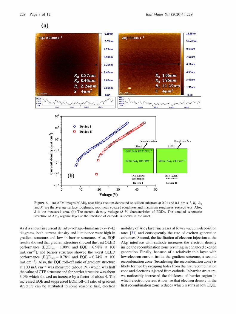
factor c.Regarding the increased electron current of Alq3 thin
films fabricated at low vacuum-deposition rates, smooth
contact area at the organic/cathode interface as a result of
low surface roughness of organic layer is considered as a
factor which can facilitate the electron injection [10,19,22].
To prove this, the surface roughness of Alq3 neat films
vacuum-deposited on silicon substrate at 0.01 and 0.1
nm s�1 was measured and depicted in figure 6a. The aver-
age surface roughness of Alq3 films increased, by a factor of
approximately four as a result of the increase in vacuum-
deposition rate. Additionally, we fabricated EODs with a
different structure of organic layer at the interface with
cathode. As it is shown in the inset of figure 6b, in device I,
we fabricated a smooth contact area using low vacuum-
deposition rate (0.01 nm s�1). But, in device II, the
deposition rate of Alq3 remained constant (0.1 nm s�1) even
at the interface with cathode.
After device fabrication, we measured the current den-
sity–voltage (J–V) characteristic of two devices. It is easily
seen a clear increase in electron current of device I relative
to device II which can be ascribed to increased electron
injection from cathode into Alq3 organic layer at low vac-
uum-deposition rate.
3.3 Introduction of novel organic layer structures
As a result of our findings, we fabricated and introduced
classic OLEDs with different structures for emitting layer
using the vacuum-deposition rate and shutter. The detailed
structures of the emitting layer are depicted in figure 7. In
constant thermal evaporation (CTE) structure the vacuum-
deposition rate remains constant, as we discussed before,
the only recombination zone is pinned at the a-NPD/Alq3interface, because of low electron and hole mobility.
Moreover, in spite of lower hole mobility in Alq3 layer,
some hole carriers pass through the emitting layer even
near cathode without radiative recombination since they
are major carriers. In other structures, in order to create
high electron injection from cathode into organic layer,
Alq3 was vacuum-deposited at the minimum deposition
rate (0.01 nm s�1). Then, we increase deposition rate to 1
nm s�1, resulting in low electron current inside the emit-
ting layer. Finally, for achieving high electron and hole
current near the a-NPD, the deposition rate again was
decreased. So, in these two novel structures (gradient and
barrier structures), the electron current is high near the
interfaces with cathode and HTL and is low inside the
emitting layer.
After device fabrication, the OLED performance was
measured and the results are shown in figure 8 and table 3.
Figure 5. (a) A pair of a-NPD molecules with a length of ‘, which are randomly oriented representing a relative
angle Du ¼ u2 � u1, angle U which indicates relative position of molecules, tip to tip intermolecular separation L and
the average intermolecular separation D. (b) Tip to tip intermolecular separation between two a-NPD molecules vs.
their relative angle (Du) at different relative positional angles (U) in the case of u1 ¼ 0�. The minimum tip to tip
separation (� 0.16 nm) occurs between two molecules which are aligned together (u1 ¼ u2 ¼U).
Bull Mater Sci (2020) 43:229 Page 7 of 12 229
As it is shown in current density–voltage–luminance (J–V–L)
diagrams, both current–density and luminance were high in
gradient structure and low in barrier structure. Also, EQE
results showed that gradient structure showed the best OLED
performance (EQEmax¼ 1:00% and EQE = 0.98% at 100
mA cm�2), and barrier structure showed the worst OLED
performance (EQEmax¼ 0:78% and EQE = 0.74% at 100
mA cm�2). Also, the EQE roll-off ratio of gradient structure
at 100 mA cm�2 was measured (about 1%) which was half
the value of CTE structure and for barrier structure was about
3.9% which showed an increase by a factor of about 4. The
increased EQE and suppressed EQE roll-off ratio of gradient
structure can be attributed to some reasons: first, electron
mobility of Alq3 layer increases at lower vacuum-deposition
rates [31] and consequently the rate of exciton generation
enhances. Second, the facilitation of electron injection at the
Alq3 interface with cathode increases the electron density
inside the recombination zone resulting in enhanced exciton
generation. Finally, because of a relatively thin layer with
low electron current inside the gradient structure, a second
recombination zone (broadening the recombination zone) is
likely formed by escaping holes from the first recombination
zone and electrons injected from cathode. In barrier structure,
we noticeably increased the thickness of barrier region in
which electron current is low, so that electron density in the
first recombination zone reduces which results in low EQE.
Figure 6. (a) AFM images of Alq3 neat films vacuum-deposited on silicon substrate at 0.01 and 0.1 nm s�1. Ra, Rq
and Rz are the average surface roughness, root mean squared roughness and maximum roughness, respectively. Also,
S is the measured area. (b) The current density–voltage (J–V) characteristics of EODs. The detailed schematic
structure of Alq3 organic layer at the interface of cathode is shown in the inset.
229 Page 8 of 12 Bull Mater Sci (2020) 43:229
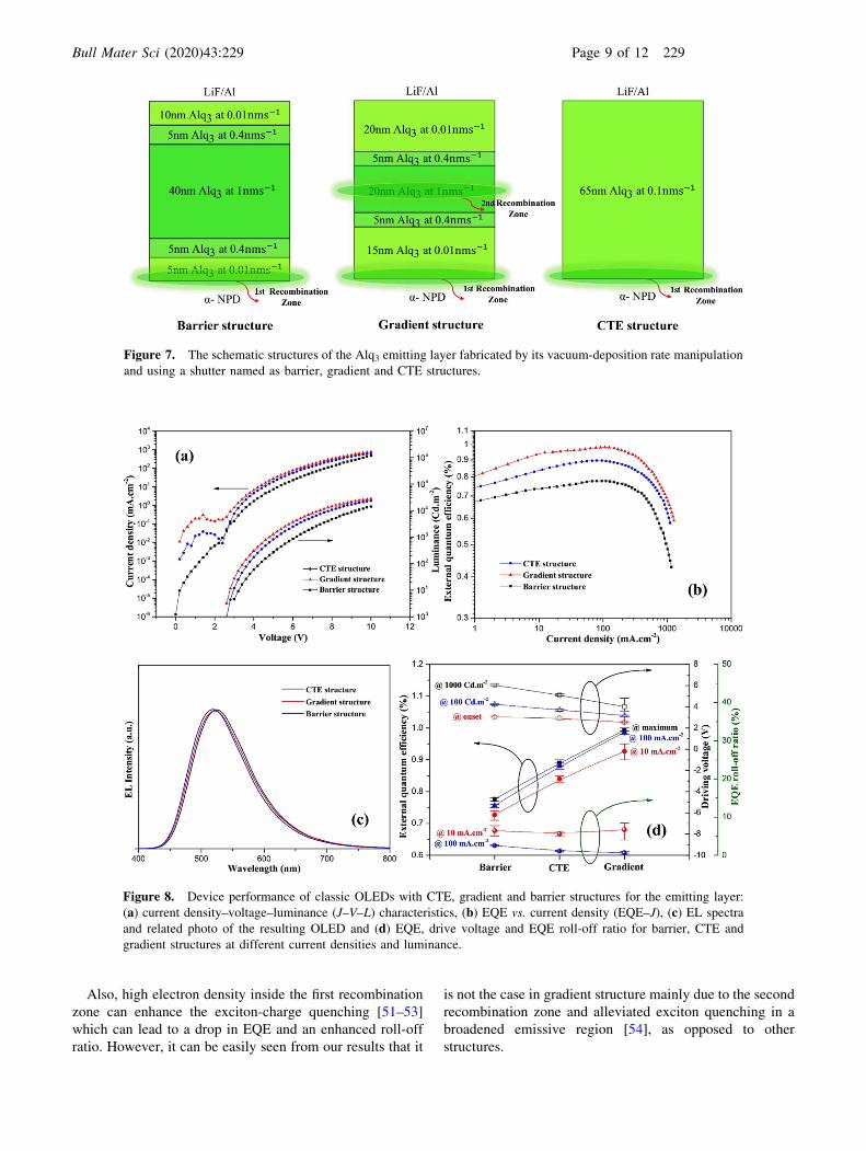
Also, high electron density inside the first recombination
zone can enhance the exciton-charge quenching [51–53]
which can lead to a drop in EQE and an enhanced roll-off
ratio. However, it can be easily seen from our results that it
is not the case in gradient structure mainly due to the second
recombination zone and alleviated exciton quenching in a
broadened emissive region [54], as opposed to other
structures.
Figure 7. The schematic structures of the Alq3 emitting layer fabricated by its vacuum-deposition rate manipulation
and using a shutter named as barrier, gradient and CTE structures.
Figure 8. Device performance of classic OLEDs with CTE, gradient and barrier structures for the emitting layer:
(a) current density–voltage–luminance (J–V–L) characteristics, (b) EQE vs. current density (EQE–J), (c) EL spectra
and related photo of the resulting OLED and (d) EQE, drive voltage and EQE roll-off ratio for barrier, CTE and
gradient structures at different current densities and luminance.
Bull Mater Sci (2020) 43:229 Page 9 of 12 229
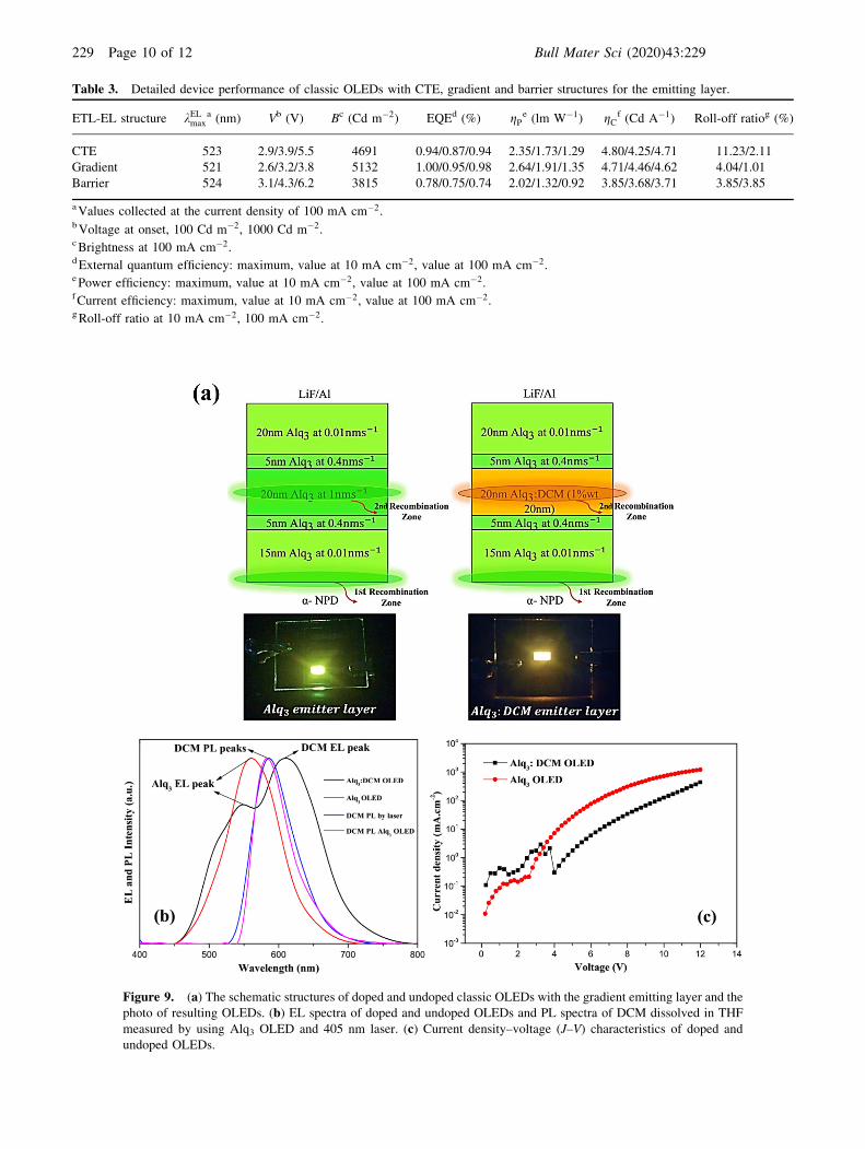
Table 3. Detailed device performance of classic OLEDs with CTE, gradient and barrier structures for the emitting layer.
ETL-EL structure kELmaxa (nm) Vb (V) Bc (Cd m�2) EQEd (%) gP
e (lm W�1) gCf (Cd A�1) Roll-off ratiog (%)
CTE 523 2.9/3.9/5.5 4691 0.94/0.87/0.94 2.35/1.73/1.29 4.80/4.25/4.71 11.23/2.11
Gradient 521 2.6/3.2/3.8 5132 1.00/0.95/0.98 2.64/1.91/1.35 4.71/4.46/4.62 4.04/1.01
Barrier 524 3.1/4.3/6.2 3815 0.78/0.75/0.74 2.02/1.32/0.92 3.85/3.68/3.71 3.85/3.85
aValues collected at the current density of 100 mA cm�2.bVoltage at onset, 100 Cd m�2, 1000 Cd m�2.cBrightness at 100 mA cm�2.dExternal quantum efficiency: maximum, value at 10 mA cm�2, value at 100 mA cm�2.ePower efficiency: maximum, value at 10 mA cm�2, value at 100 mA cm�2.fCurrent efficiency: maximum, value at 10 mA cm�2, value at 100 mA cm�2.gRoll-off ratio at 10 mA cm�2, 100 mA cm�2.
Figure 9. (a) The schematic structures of doped and undoped classic OLEDs with the gradient emitting layer and the
photo of resulting OLEDs. (b) EL spectra of doped and undoped OLEDs and PL spectra of DCM dissolved in THF
measured by using Alq3 OLED and 405 nm laser. (c) Current density–voltage (J–V) characteristics of doped and
undoped OLEDs.
229 Page 10 of 12 Bull Mater Sci (2020) 43:229
In order to further improve our understanding regarding
the charge transport mechanism inside the emitting layer
and elucidate the electron–hole recombination process and
region in our new structures, we fabricated another gradient
device in which 1% by weight DCM was doped in the high
deposition rate region, according to figure 9a. Next, we
measured the EL spectra and compared with conventional
device. Figure 9b illustrates EL spectra for undoped and
doped gradient devices representing a single peak and a
double peak, respectively. The second peak in red region is
attributed to electroluminescent radiation of DCM indicated
another recombination zone inside the Alq3 emitting layer.
Moreover, the shapes of PL spectra associated with the
sample of DCM dissolved in tetrahydrofuran (THF) at a
concentration of 0.1 mg ml-1 which was excited using
undoped classic OLED and 405 nm solid state laser, are
depicted in figure 9b. The comparison between EL spectra
of doped gradient OLED and PL spectra of DCM solution
excited by undoped classic OLED indicates that the DCM
peak related to emission spectra of doped gradient OLED is
generated probably due to the EL emission rather than the
PL emission.
Therefore, we speculate that fabrication of a second
recombination region for electrons and holes in our novel
structures only by controlling the deposition rate during
device fabrication is possible. However, more studies are
needed to be performed to characterize our new structures.
4. Conclusion
In this paper we evaluated the influence of HTL and ETL
vacuum-deposition rate on classic and TADF OLED per-
formance, respectively. We concluded from EQE mea-
surements that charge carrier balance factor had a key role
in changing device efficiency because deposition rate
manipulation changes charge carrier mobility and conse-
quently, the charge density inside the recombination zone.
Moreover, our analytical model associated with a-NPD thin
films revealed that horizontally oriented molecules caused a
decrease in intermolecular separation regardless of organic
layer density, resulting in enhanced hole hopping rate.
Additionally, we demonstrated that high electron current
density at low deposition rate in Alq3 ETL is attributed to
high electron injection from cathode as a result of low
surface roughness of organic layer at the interface with
cathode. Finally, we fabricated and introduced new gradient
and barrier emitting layer structures using vacuum-deposi-
tion rate control to create an extra-recombination zone
which resulted in increasing radiative recombination of
electrons and holes and device efficiency. Our findings can
open a new way to enhance the efficiency of OLEDs by
controlling the vacuum-deposition rate of organic layers
during the deposition process. It can also reduce the time of
fabrication process using organic layers with high electrical
characteristics at high deposition rates.
Acknowledgements
Classic and TADF OLEDs were fabricated and character-
ized in the Centre for Organic Photonics and Electronics
Research (OPERA), Kyushu University, 744 Motooka,
Nishi, Fukuoka 819-0395, Japan. We would like to
appreciate Professor Chihaya Adachi and Toshinori Mat-
sushima for their sincere advice.
References
[1] Chan C-Y, Tanaka M, Nakanotani H and Adachi C 2018
Nat. Commun. 9 5036
[2] Chiba T, Kumagai D, Udagawa K, Watanabe Y and Kido J
2018 Sci. Rep. 8 11472
[3] Liu Y, Li C, Ren Z, Yan S and Bryce M R 2018 Nat. Rev.
Mater. 3 18020
[4] Kim D-H, D’Aleo A, Chen X-K, Sandanayaka A D S, Yao
D, Zhao L et al 2018 Nat. Photonics 12 98
[5] Zhao Y, Yun F, Huang Y, Wu Z, Li Y, Jiao B et al 2016
Appl. Phys. Lett. 109 13303
[6] Matsushima T, Qin C, Goushi K, Bencheikh F, Komino T,
Leyden M et al 2018 Adv. Mater. 30 1802662
[7] Fujimoto H, Suekane T, Imanishi K, Yukiwaki S, Wei H,
Nagayoshi K et al 2016 Sci. Rep. 6 38482
[8] Mu H, Shen H and Klotzkin D 2004 Solid State Electron. 482085
[9] Matsushima T, Shiomura K, Naka S and Murata H 2012 Thin
Solid Films 520 2283
[10] Lee P-T, Chang T-Y and Chen S-Y 2008 Org. Electron. 9916
[11] Fischer J, Widmer J, Kleemann H, Tress W, Koerner C,
Riede M et al 2015 J. Appl. Phys. 117 45501
[12] Kanbur H, Voigt M, Sahingoz R 2013 J. Mater. Sci.: Mater.
Electron. 24 4833
[13] Lu N, Li L, Geng D and Liu M 2018 Org. Electron. 61 223
[14] Suzuki F, Kubo S, Fukushima T and Kaji H 2018 Sci. Rep. 85203
[15] Hauke A, Widmer J, Kasemann D and Leo K 2015 Appl.
Phys. Lett. 106 233301
[16] Rolin C, Kang E, Lee J-H, Borghs G, Heremans P and Genoe
J 2017 Nat. Commun. 8 14975
[17] Esaki Y, Komino T, Matsushima T and Adachi C 2017 J.
Phys. Chem. Lett. 8 5891
[18] Liu S-W, Lee C-C, Wang C-H, Lee J-H, Chen C-T and
Wang J-K 2009 Chem. Phys. Lett. 474 207
[19] Liu S-W, Lee C-C, Chang Y-T, Lee J-H, Chen C-T and
Wang J-K 2014 Int. J. Photoenergy 2014 412084
[20] Lee C B, Uddin A, Hu X and Andersson T G 2004 Mater.
Sci. Eng. B 112 14
[21] Videlot-Ackermann C, Diallo A K, Brisset H, Fages F,
Serein-Spirau F, Lere-Porte J-P et al 2010 Optoelectron.
Adv. Mater. Rapid Commun. 4 699
[22] Mikaeili A, Matsushima T, Esaki Y, Yazdani S A, Adachi C
and Mohajerani E 2019 Opt. Mater. 91 93
[23] Noguchi Y, Kim H-J, Ishino R, Goushi K, Adachi C,
Nakayama Y et al 2015 Org. Electron. 17 184
Bull Mater Sci (2020) 43:229 Page 11 of 12 229
[24] Cui L-S, Ruan S-B, Bencheikh F, Nagata R, Zhang L, Inada
K et al 2017 Nat. Commun. 8 2250
[25] Furukawa T, Nakanotani H, Inoue M and Adachi C 2015 Sci.
Rep. 5 8429
[26] Nakanotani H, Higuchi T, Furukawa T, Masui K, Morimoto
K, Numata M et al 2014 Nat. Commun. 5 4016
[27] Noda H, Nakanotani H and Adachi C 2018 Sci. Adv. 4eaao6910
[28] Wu T-L, Huang M-J, Lin C-C, Huang P-Y, Chou T-Y, Chen-
Cheng R-W et al 2018 Nat. Photonics 12 235
[29] Kuwae H, Nitta A, Yoshida K, Kasahara T, Matsushima T,
Inoue M et al 2015 J. Appl. Phys. 118 155501
[30] Yu Y, Ma L, Wang D, Zhou H, Yao B and Wu Z 2017 Org.
Electron. 51 173
[31] Chen B J, Lai W Y, Gao Z Q, Lee C S, Lee S and Gambling
W A 1999 Appl. Phys. Lett. 75 4010
[32] Lin T-C, Hsiao C-H and Lee J-H 2005 Proc SPIE 5937[33] Matsumoto N and Adachi C 2010 J. Phys. Chem. C 114
4652
[34] Maasoumi F, Jansen-van Vuuren R D, Shaw P E, Puttock
E V, Nagiri R C R, McEwan J A et al 2018 NPJ Flexible
Electron. 2 27
[35] Lee S, Koo H, Kwon O, Jae Park Y, Choi H, Lee K et al
2017 Sci. Rep. 7 11995
[36] Qin D, Liu J, Chen Y, Chen L, Quan W, and Li G 2012
Semicond. Sci. Technol. 27 045012
[37] Qiu J, Wang Z B, Helander M and Lu Z H 2011 Appl. Phys.
Lett. 99 153305
[38] Scott J C and Malliaras G G 1999 Chem. Phys. Lett. 299 115
[39] Wang Z B, Helander M G, Greiner M T, Qiu J and Lu Z H
2009 Phys. Rev. B 80 235325
[40] Wang Z B, Helander M G, Greiner M T, Qiu J and Lu Z H
2010 J. Appl. Phys. 107 34506
[41] Deng W-Q, Sun L, Huang J-D, Chai S, Wen S-H and Han
K-L 2015 Nat. Protoc. 10 632
[42] Tessler N, Preezant Y, Rappaport N and Roichman Y 2009
Adv. Mater. 21 2741
[43] Athanasopoulos S, Kirkpatrick J, Martınez D, Frost J M,
Foden C M, Walker A B et al 2007 Nano Lett. 7 1785
[44] Lin B C, Cheng C P and Lao Z P M 2003 J. Phys. Chem. A
107 5241
[45] So F 2009 Organic electronics: materials, processing,
devices and applications. CRC Press. ISBN 9781420072907
[46] Shi Y-R, Wei H-L, Jia X-B and Liu Y 2018 J. Mater. Sci. 53[47] Xiang H-F, Xu Z-X, Roy V A L, Che C-M and Lai P T 2007
Rev. Sci. Instrum. 78 34104
[48] Matsushima T, Esaki Y and Adachi C 2014 Appl. Phys. Lett.
105 243301
[49] Fei C, Liu H, Wang X, Zhao L, Zhao D and Feng X 2017
Nanoscale Res. Lett. 12 218
[50] Chakaroun M, Antony R, Fischer A P A, Ratier B, Moliton
A, Lee M W et al 2013 Solid State Sci. 15 84
[51] Burin A L and Ratner M A 2000 J. Phys. Chem. A 104 4704
[52] Ingram G L and Lu Z-H 2014 J. Photonics Energy 4 040993
[53] Li S H, Wu S F, Wang Y K, Liang J J, Sun Q, Huang C C
et al 2018 J. Mater. Chem. C 6 342
[54] Wu Z, Liu Y, Yu L, Zhao C, Yang D, Qiao X et al 2019 Nat.
Commun. 10 1
229 Page 12 of 12 Bull Mater Sci (2020) 43:229