Embed Size (px)
Citation preview
Non conventional Processes7ME6A (Part IV)
Er. Mohit OstwalAssistant ProfessorDepartment of Mechanical EngineeringJodhpur Institute of Engineering and Technology-Coed
LASER Micromachining• Laser micromachining is based on the interaction of light with solid
matter. As a result of the complex interaction between light and matter, small amounts of material can be removed from the surface.
1. Pyrolithic processing is composed of heating, melting and ablating the material at the surface.2. Photolithic processing is based on the direct breaking of chemical bonds in a wide range of materials.
• Monochromatic light source
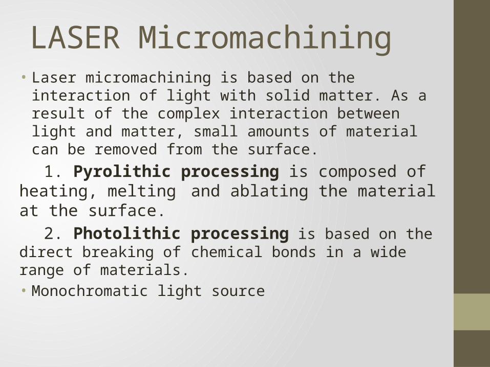
Fundamentals of LASERSTIMULATED EMISSION• The pumping mechanism raises the energy level of an atom,
and after a short period of time the atom tries to return to its original state of energy. To do this it ejects energy in form of a photon.
STIMULATED EMISSION• If the temperature of the cavity is too high the lower energy
level cannot be transferred to its ground state fast enough, thus causing the production of LASER light.
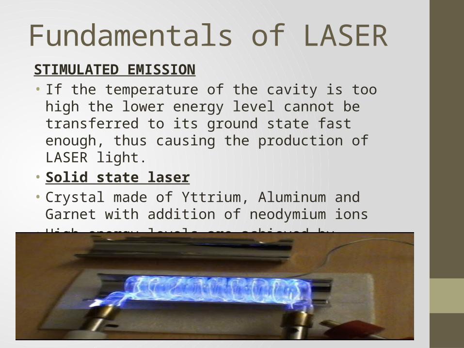
• Solid state laser• Crystal made of Yttrium, Aluminum and Garnet with addition
of neodymium ions• High energy levels are achieved by neodymium ions.• Energy is supplied by a flash lamp.
Fundamentals of LASER

• Q-Switch is a way of controlling beam of LASER1. Mechanical Chopper
Fundamentals of LASER
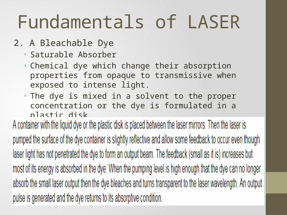
2. A Bleachable Dye• Saturable Absorber• Chemical dye which change their absorption properties from opaque
to transmissive when exposed to intense light.• The dye is mixed in a solvent to the proper concentration or the dye is
formulated in a plastic disk.
Fundamentals of LASER
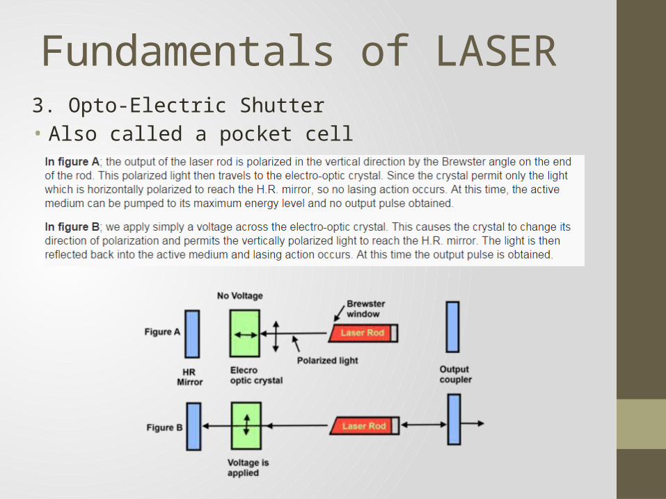
3. Opto-Electric Shutter• Also called a pocket cell
Fundamentals of LASER
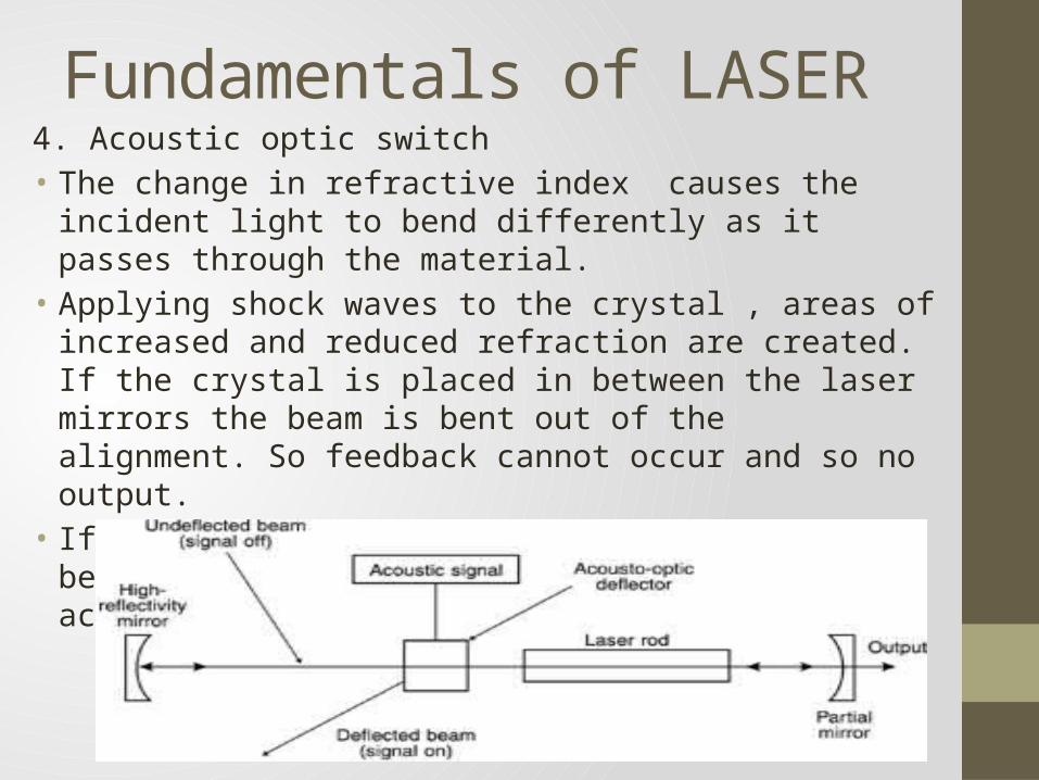
4. Acoustic optic switch• The change in refractive index causes the incident light to bend
differently as it passes through the material.• Applying shock waves to the crystal , areas of increased and reduced
refraction are created. If the crystal is placed in between the laser mirrors the beam is bent out of the alignment. So feedback cannot occur and so no output.
• If mechanical pressure is stopped then the beam will go in alignment and feedback is achieved and as a result output is obtained.
Fundamentals of LASER
Types of LASER• Diode LASER• Ti-Sapphire LASERa) Short Low powered nanojoule femtosecond pulses are created.b) Chirped pulse amplification(CPA)- Pulse is stretched , amplified
and then compressed to create a high intensity femtosecond pulse.
c) Femtosecond- 10−15
Picosecond- 10−12
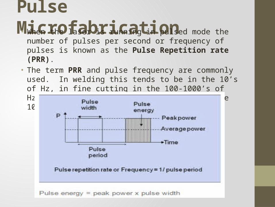
Pulse Microfabrication• When the laser is running in pulsed mode the number of pulses per
second or frequency of pulses is known as the Pulse Repetition rate (PRR).
• The term PRR and pulse frequency are commonly used. In welding this tends to be in the 10’s of Hz, in fine cutting in the 100-1000’s of Hz, and in marking or micro machining in the 10,000’s of Hz.
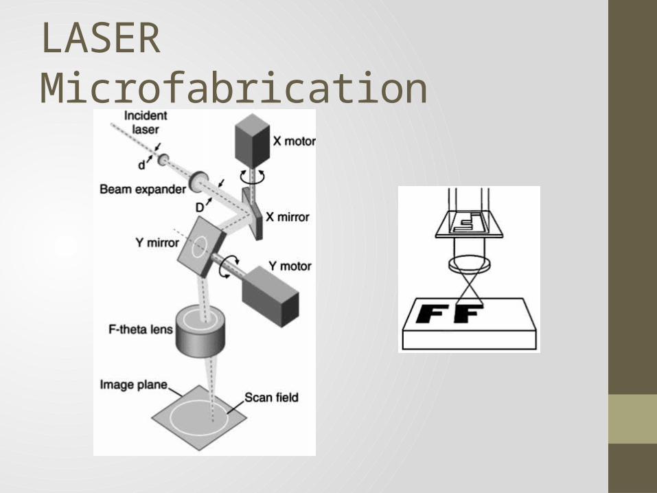
LASER Microfabrication
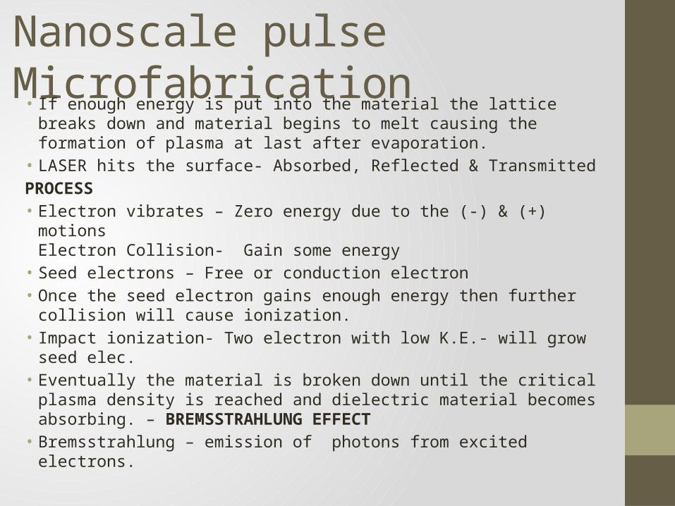
Nanoscale pulse Microfabrication• If enough energy is put into the material the lattice breaks down
and material begins to melt causing the formation of plasma at last after evaporation.
• LASER hits the surface- Absorbed, Reflected & TransmittedPROCESS• Electron vibrates – Zero energy due to the (-) & (+) motions
Electron Collision- Gain some energy• Seed electrons – Free or conduction electron• Once the seed electron gains enough energy then further collision
will cause ionization.• Impact ionization- Two electron with low K.E.- will grow seed elec.• Eventually the material is broken down until the critical plasma
density is reached and dielectric material becomes absorbing. – BREMSSTRAHLUNG EFFECT
• Bremsstrahlung – emission of photons from excited electrons.
Nanoscale pulse Microfabrication• Thus after a period of time sufficient energy is absorbed and
transferred to electron, which inturn heat the material and causes melting and evaporation.
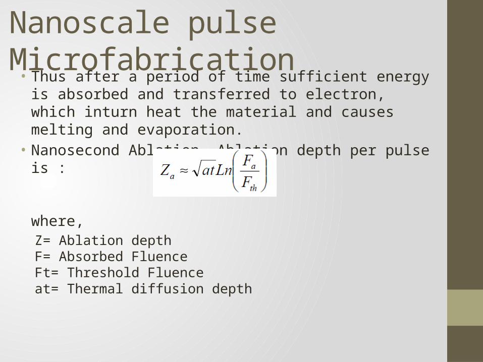
• Nanosecond Ablation- Ablation depth per pulse is :
where,Z= Ablation depthF= Absorbed FluenceFt= Threshold Fluenceat= Thermal diffusion depth
Shielding Gas (PLASMA)• Plasma is a hot ionized gas consisting of equal no. of positively
charged ions and negatively charged electrons.• Exposed material is protected by plasma – oxidation• If the plasma is ionized and the conditions are appropriate, the
plasma can acquire energy from the incoming beam such that it moves away from the surface and heads toward the source of the beam.
• In some cases, it blocks the path of the laser beam to the substrate and machining is halted.
• Often helium, argon, neon and oxygen gases are used; the type of gas used depends upon the reactions that take place
• Some gases are limited due the difficulties in ionization.
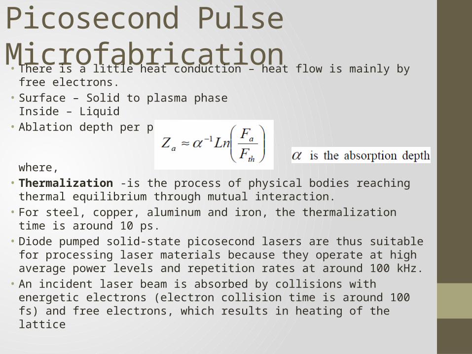
Picosecond Pulse Microfabrication• There is a little heat conduction – heat flow is mainly by free electrons.• Surface – Solid to plasma phase
Inside – Liquid• Ablation depth per pulse is
where, • Thermalization -is the process of physical bodies reaching thermal
equilibrium through mutual interaction.• For steel, copper, aluminum and iron, the thermalization time is around 10
ps.• Diode pumped solid-state picosecond lasers are thus suitable for processing
laser materials because they operate at high average power levels and repetition rates at around 100 kHz.
• An incident laser beam is absorbed by collisions with energetic electrons (electron collision time is around 100 fs) and free electrons, which results in heating of the lattice
Picosecond Pulse Microfabrication• Surface structuring or surface modification is possible with
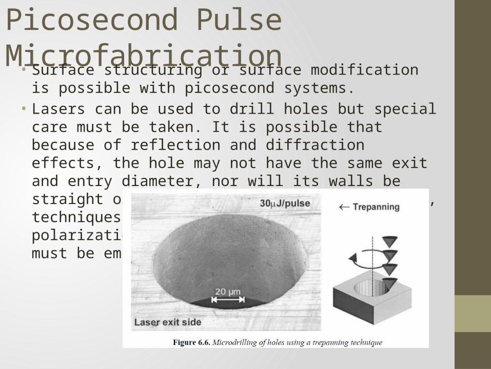
picosecond systems.• Lasers can be used to drill holes but special care must be taken. It is
possible that because of reflection and diffraction effects, the hole may not have the same exit and entry diameter, nor will its walls be straight or parallel. To counter this effect, techniques such as helical drilling and polarization control with trepanning optics must be employed.

Picosecond Pulse Microfabrication
Femtosecond Pulse Microfabrication• An electromagnetic wave interacts with the particle, multi-photon
absorption occurs, and there is no liquid phase.• The pulse and the evaporation interaction occur before the next
pulse impacts the material.• Bounded electrons of the material can be directly ionized by multi-
photon absorption.• The electron does not have to wait for energy to be supplied to it.
The pulse is so short that the energy is supplied at a rate where direct ionization occurs.
• The breakdown fluence threshold can be defined as the fluence at which there is a 50% probability that a laser of this pulse width and fluence will cause breakdown to occur.
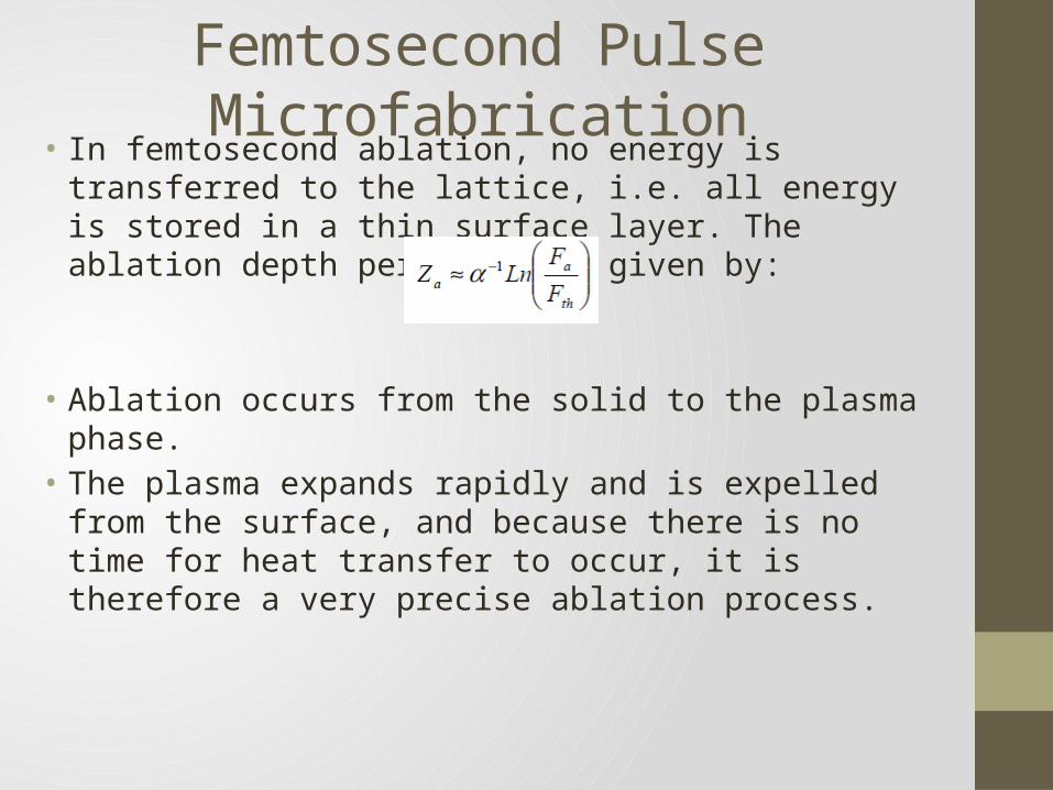
Femtosecond Pulse Microfabrication• In femtosecond ablation, no energy is transferred to the lattice, i.e.
all energy is stored in a thin surface layer. The ablation depth per pulse is given by:
• Ablation occurs from the solid to the plasma phase. • The plasma expands rapidly and is expelled from the surface, and
because there is no time for heat transfer to occur, it is therefore a very precise ablation process.
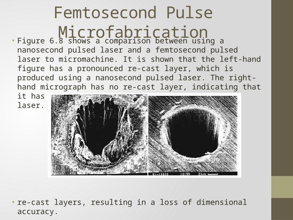
Femtosecond Pulse Microfabrication• Figure 6.8 shows a comparison between using a nanosecond
pulsed laser and a femtosecond pulsed laser to micromachine. It is shown that the left-hand figure has a pronounced re-cast layer, which is produced using a nanosecond pulsed laser. The right-hand micrograph has no re-cast layer, indicating that it has been machined using a femtosecond pulsed laser.
• re-cast layers, resulting in a loss of dimensional accuracy.
Topics to be covered by self study• Effects of nanosecond pulsed Microfabrication,• Laser Nanofabrication• Plus a review of the topics covered in the presentation from
the suggested books.