Embed Size (px)
Citation preview

NATIONAL INSTITUTE OF
MECHATRONICS ENGINEERING
N.W.F.P. UNIVERSITY OF ENGINEERING AND TECHNOLOGY, PESHAWAR
Electronic Circuit Design
LAB MANUAL
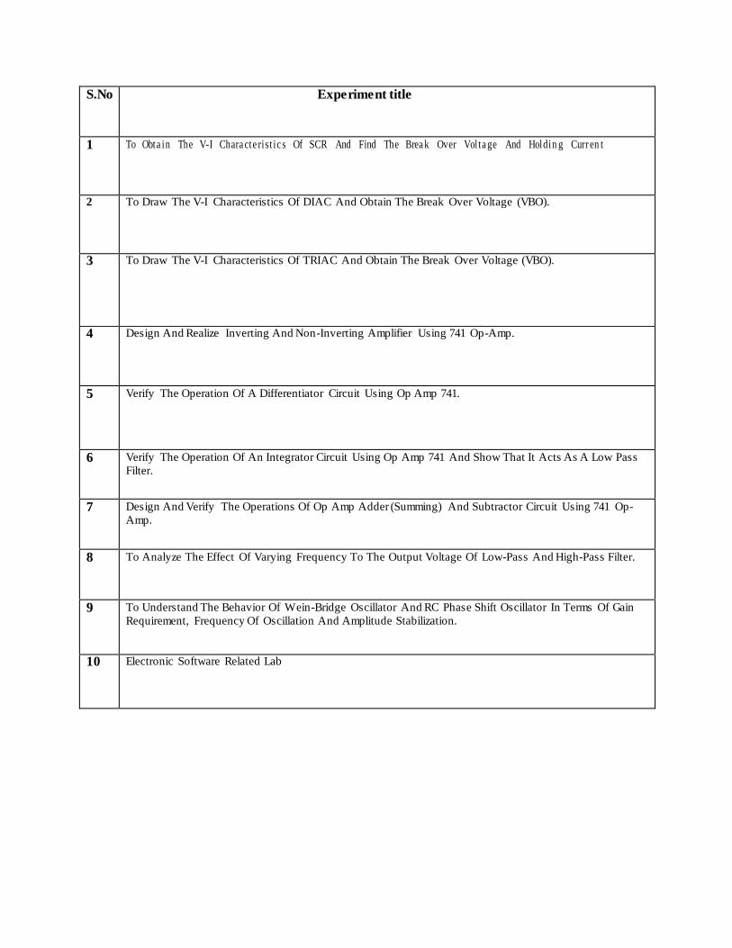
S.No Experiment title
1 To Obta in The V-I Chara cte rist ic s Of SCR And Find The Brea k Over Vol ta ge And Holdin g Curr en t
2 To Draw The V-I Characteristics Of DIAC And Obtain The Break Over Voltage (VBO).
3 To Draw The V-I Characteristics Of TRIAC And Obtain The Break Over Voltage (VBO).
4 Design And Realize Inverting And Non-Inverting Amplifier Using 741 Op-Amp.
5 Verify The Operation Of A Differentiator Circuit Using Op Amp 741.
6 Verify The Operation Of An Integrator Circuit Using Op Amp 741 And Show That It Acts As A Low Pass
Filter.
7 Design And Verify The Operations Of Op Amp Adder (Summing) And Subtractor Circuit Using 741 Op-
Amp.
8 To Analyze The Effect Of Varying Frequency To The Output Voltage Of Low-Pass And High-Pass Filter.
9 To Understand The Behavior Of Wein-Bridge Oscillator And RC Phase Shift Oscillator In Terms Of Gain
Requirement, Frequency Of Oscillation And Amplitude Stabilization.
10 Electronic Software Related Lab
EXPERIMENT No 1
CHARAC TERISTIC S OF SCR
Aim:
TO OBTA IN THE V-I CHA RA CT E RIST IC S OF SCR AND FIND THE BRE AK OVER VOL TA GE AND HOLD ING CUR RE NT .
APPARATUS REQUIRED:-
Variable Power Supply Voltmeter Amphere Meter
COMPONENTS REQUIRED:-
SCR TYN WIRES RESISTOR
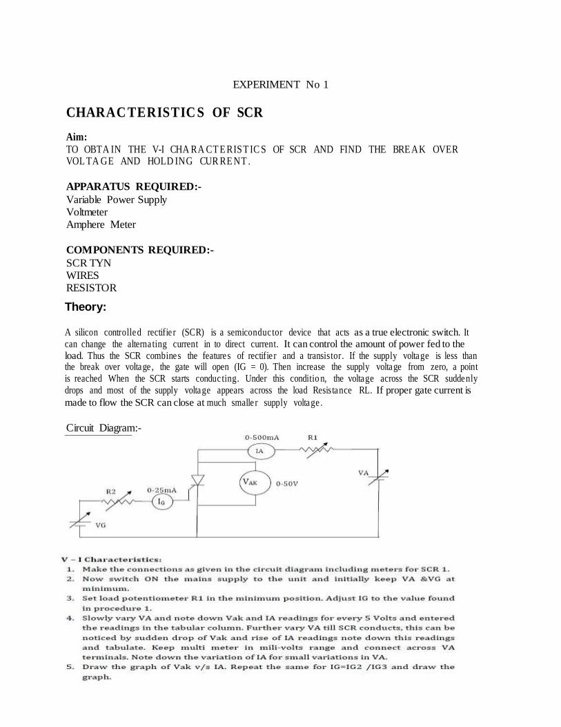
Circuit Diagram:-
Theory:
A silicon controlled rectifie r (SCR) is a semiconduc tor device that acts as a true electronic switch. It can change the alterna ting current in to direct current. It can control the amount of power fed to the load. Thus the SCR combines the features of rectifie r and a transistor. If the supply voltage is less than the break over voltage , the gate will open (IG = 0). Then increase the supply voltage from zero, a point is reached When the SCR starts conduc ting. Under this conditio n, the voltage across the SCR suddenly drops and most of the supply voltage appears across the load Resistance RL. If proper gate current is
made to flow the SCR can close at much smalle r supply voltage .
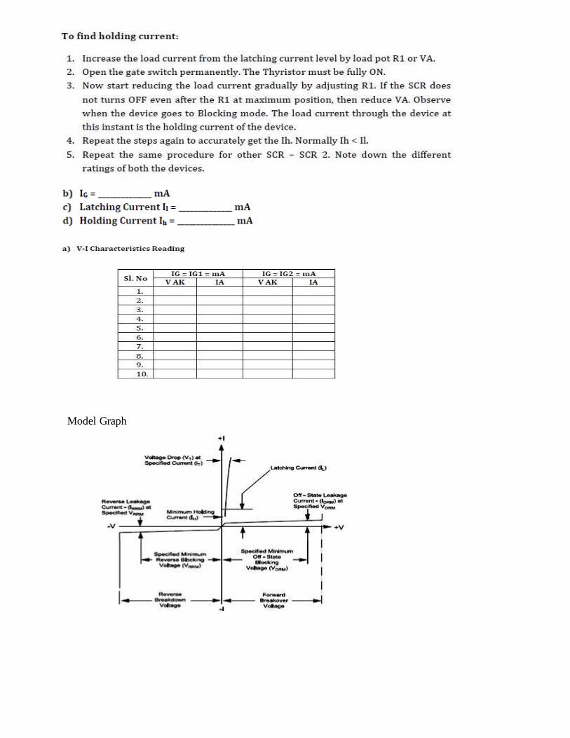
Model Graph
Experiment no 2
Characteristics of DIAC
Aim:
To draw the V-I characteristics of DIAC and obtain the break over voltage (VBO).
APPARATUS REQUIRED:-
Variable Power Supply Voltmeter
Amphere Meter
COMPONENTS REQUIRED:-
DIAC SSD3A WIRES
RESISTOR 5KΩ, IKΩ
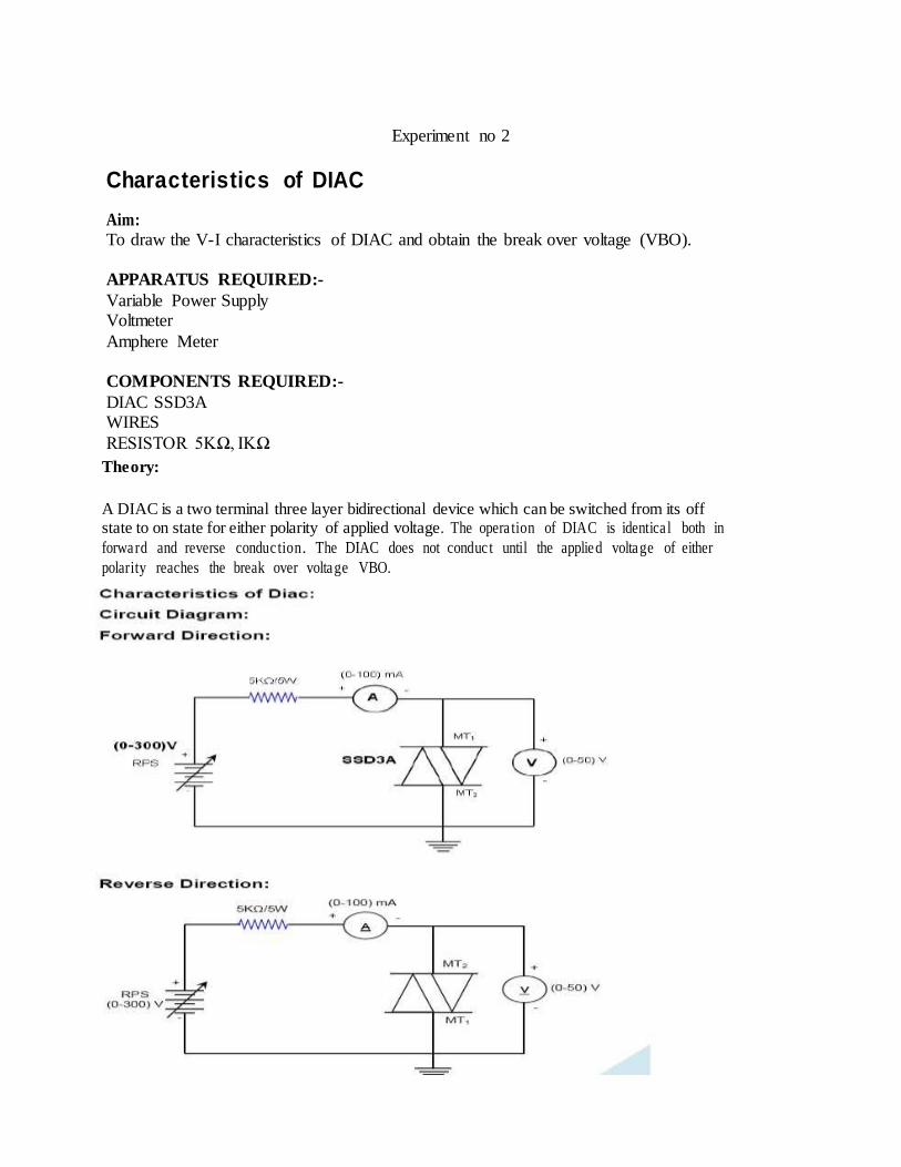
Theory:
A DIAC is a two terminal three layer bidirectional device which can be switched from its off state to on state for either polarity of applied voltage. The opera tion of DIAC is identica l both in
forward and reverse conduc tion. The DIAC does not conduc t until the applied voltage of either
polarity reaches the break over voltage VBO.
Procedure:-
Diac Characteristics:
The connections are made as shown in the circuit diagram . First DIAC is connected in forward direction
The input supply is increased in step by step by varying the RPS The corresponding ammeter and voltmeter readings are noted and tabulated . Then the DIAC is connected in revers e condition.
The above process is repeated
Observation
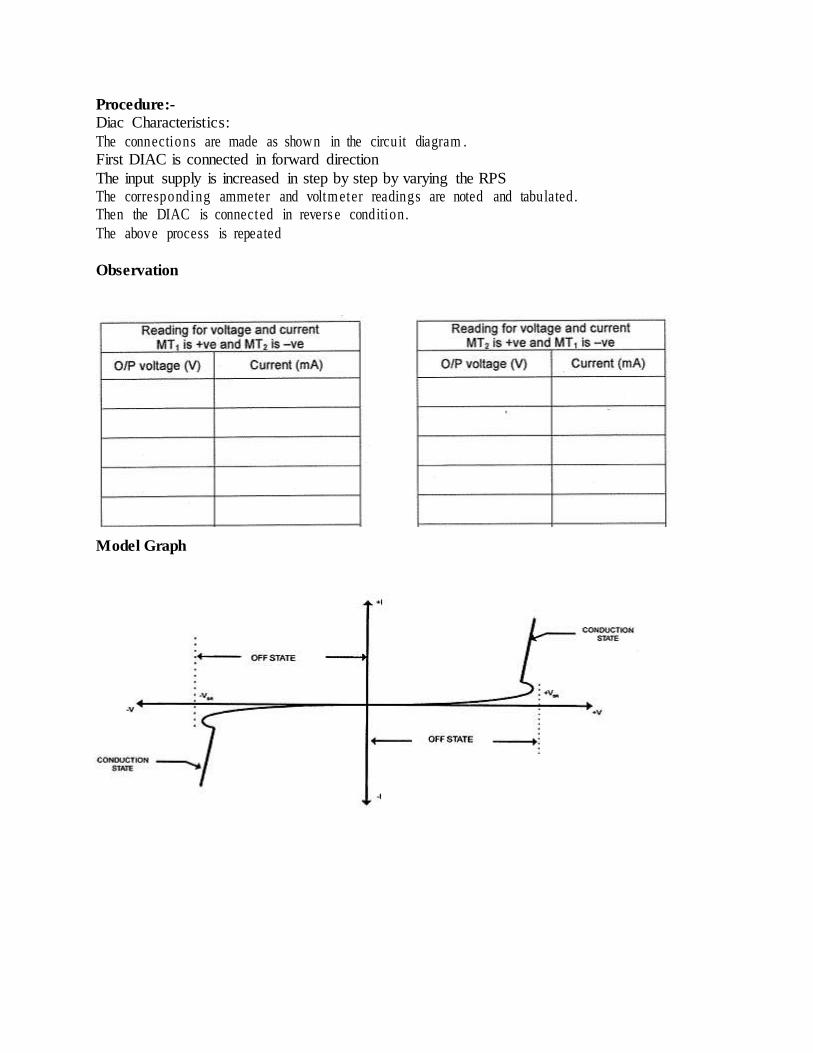
Model Graph
Experiments no 3
Characteristics of TRIAC
Aim: To draw the V-I characteristics of TRIAC and obtain the break over voltage (VBO).
APPARATUS REQUIRED:-
Variable Power Supply
Voltmeter Amphere Meter
COMPONENTS REQUIRED:-
TRIAC BTM36
Resistor 5KΩ, IKΩ Connecting Wire
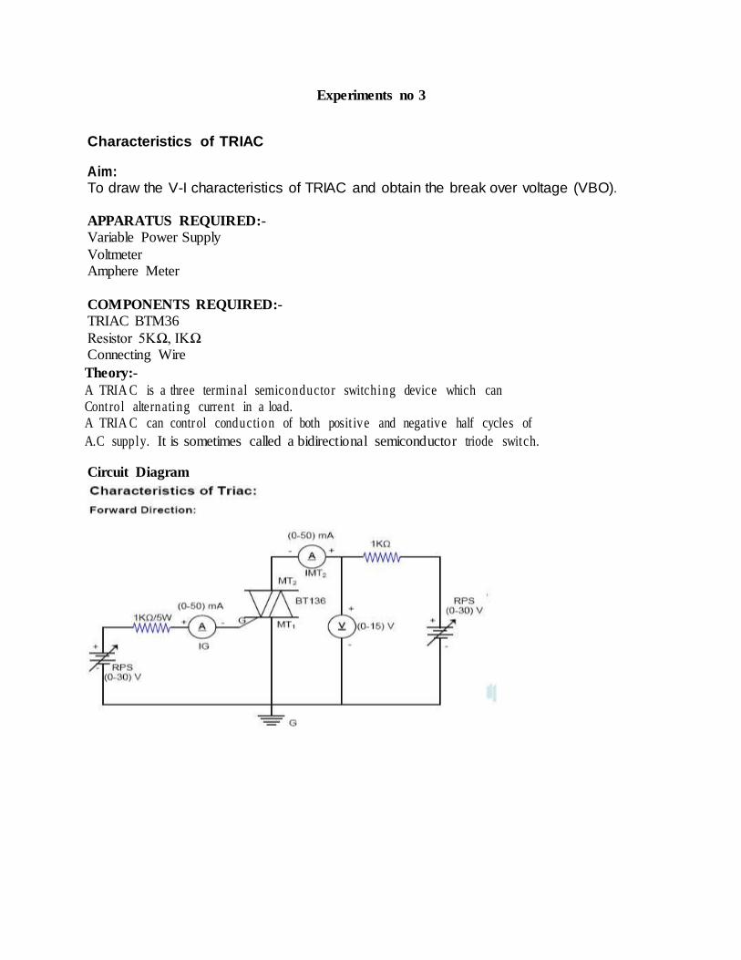
Circuit Diagram
Theory:-
A TRIA C is a three terminal semiconductor switching device which can Control alternating current in a load. A TRIA C can control conduction of both posit ive and negative half cycles of
A.C supply. It is sometimes called a bidirectional semiconductor triode switch.
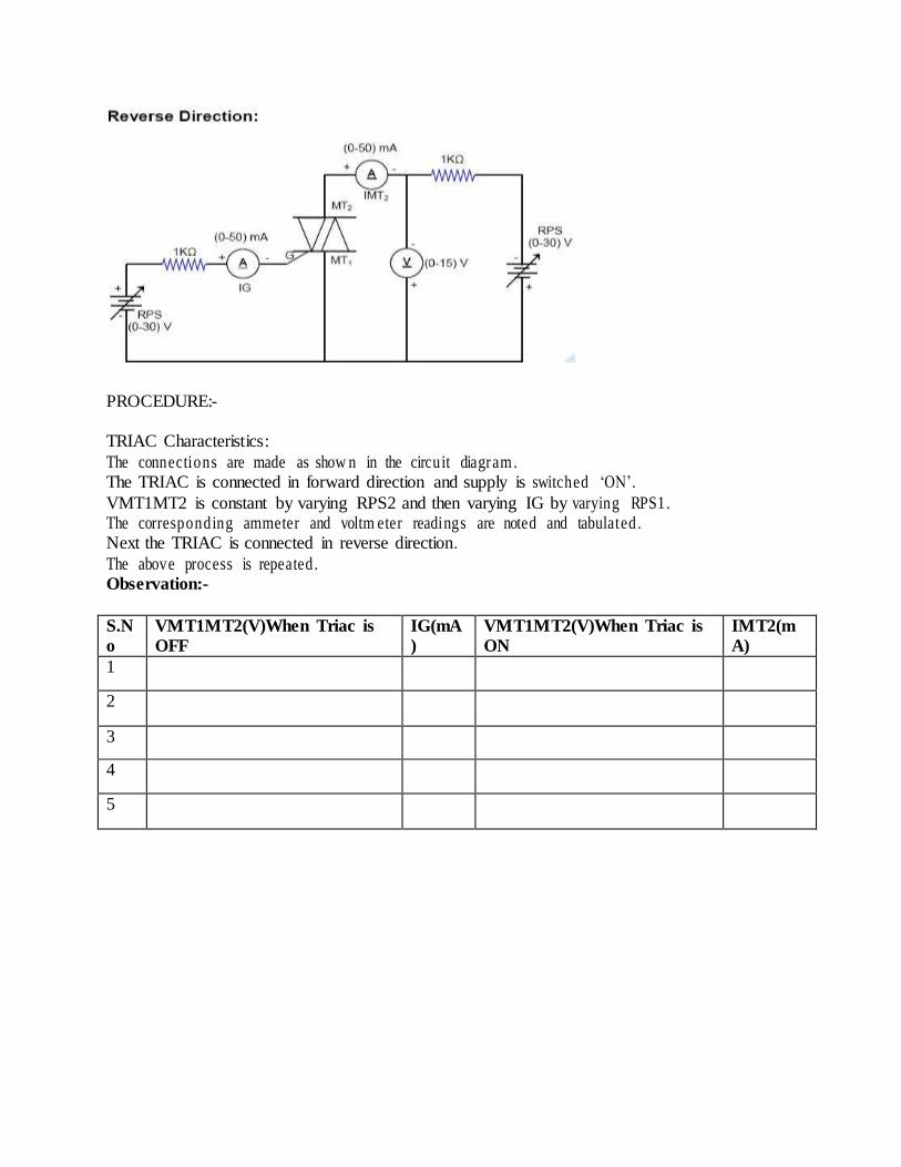
PROCEDURE:- TRIAC Characteristics:
The connections are made as show n in the circuit diagram . The TRIAC is connected in forward direction and supply is switched ‘ON’.
VMT1MT2 is constant by varying RPS2 and then varying IG by varying RPS1. The corresponding ammeter and voltm eter readings are noted and tabulated . Next the TRIAC is connected in reverse direction.
The above process is repeated . Observation:-
S.N
o
VMT1MT2(V)When Triac is
OFF
IG(mA
)
VMT1MT2(V)When Triac is
ON
IMT2(m
A)
1
2
3
4
5
Experiment No 4
Aim Design and realize Inverting and Non-inverting amplifier using 741 Op-amp.
Apparatus Required:
CRO, Function Generator, Bread Board, 741 IC, ±12V supply, Resistors 1KΩ, 10KΩ, and
connecting leads.
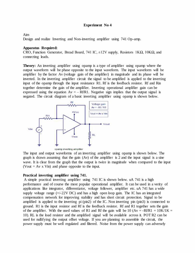
Theory: An inverting amplifier using opamp is a type of amplifier using opamp where the output waveform will be phase opposite to the input waveform. The input waveform will be amplifier by the factor Av (voltage gain of the amplifier) in magnitude and its phase will be
inverted. In the inverting amplifier circuit the signal to be amplified is applied to the inverting input of the opamp through the input resistance R1. Rf is the feedback resistor. Rf and Rin
together determine the gain of the amplifier. Inverting operational amplifier gain can be expressed using the equation Av = – Rf/R1. Negative sign implies that the output signal is negated. The circuit diagram of a basic inverting amplifier using opamp is shown below.
The input and output waveforms of an inverting amplifier using opamp is shown below. The graph is drawn assuming that the gain (Av) of the amplifier is 2 and the input signal is a sine
wave. It is clear from the graph that the output is twice in magnitude when compared to the input (Vout = Av x Vin) and phase opposite to the input.
Practical inverting amplifier using 741.
A simple practical inverting amplifier using 741 IC is shown below. uA 741 is a high
performance and of course the most popular operational amplifier. It can be used in a verity of applications like integrator, differentiator, voltage follower, amplifier etc. uA 741 has a wide
supply voltage range (+/-22V DC) and has a high open loop gain. The IC has an integrated compensation network for improving stability and has short circuit protection. Signal to be amplified is applied to the inverting pi (pin2) of the IC. Non inverting pin (pin3) is connected to
ground. R1 is the input resistor and Rf is the feedback resistor. Rf and R1 together sets the gain of the amplifier. With the used values of R1 and Rf the gain will be 10 (Av = -Rf/R1 = 10K/1K =
10). RL is the load resistor and the amplified signal will be available across it. POT R2 can be used for nullifying the output offset voltage. If you are planning to assemble the circuit, the power supply must be well regulated and filtered. Noise from the power supply can adversely
affect the performance of the circuit. When assembling on PCB it is recommended to mount the IC on the board using an IC base.
In the inverting amplifier only one input is applied and that is to the inverting input (V2) terminal. The Non inverting input terminal (V1) is grounded. Since, V1=0 V& V2=Vin Vo= -A
Vin The negative sign indicates the output voltage is 1800 out of phase with respect to the input and amplified by gain A.
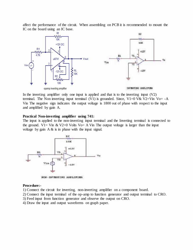
Practical Non-inverting amplifier using 741:
The input is applied to the non-inverting input terminal and the Inverting terminal is connected to
the ground. V1= Vin & V2=0 Volts Vo= A Vin The output voltage is larger than the input voltage by gain A & is in phase with the input signal.
Procedure:- 1) Connect the circuit for inverting, non-inverting amplifier on a component board.
2) Connect the input terminal of the op-amp to function generator and output terminal to CRO. 3) Feed input from function generator and observe the output on CRO. 4) Draw the input and output waveforms on graph paper.
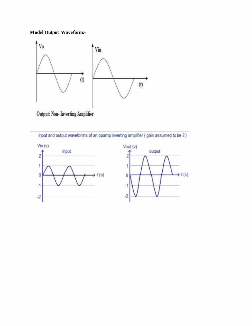
Model Output Waveform:-
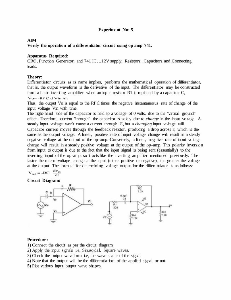
Experiment No: 5
AIM
Verify the operation of a differentiator circuit using op amp 741.
Apparatus Required:
CRO, Function Generator, and 741 IC, ±12V supply, Resistors, Capacitors and Connecting
leads.
Theory: Differentiator circuits as its name implies, performs the mathematical operation of differentiator, that is, the output waveform is the derivative of the input. The differentiator may be constructed
from a basic inverting amplifier when an input resistor R1 is replaced by a capacitor C,
Thus, the output Vo is equal to the Rf C times the negative instantaneous rate of change of the input voltage Vin with time. The right-hand side of the capacitor is held to a voltage of 0 volts, due to the "virtual ground"
effect. Therefore, current "through" the capacitor is solely due to change in the input voltage. A steady input voltage won't cause a current through C, but a changing input voltage will.
Capacitor current moves through the feedback resistor, producing a drop across it, which is the same as the output voltage. A linear, positive rate of input voltage change will result in a steady negative voltage at the output of the op-amp. Conversely, a linear, negative rate of input voltage
change will result in a steady positive voltage at the output of the op-amp. This polarity inversion from input to output is due to the fact that the input signal is being sent (essentially) to the
inverting input of the op-amp, so it acts like the inverting amplifier mentioned previously. The faster the rate of voltage change at the input (either positive or negative), the greater the voltage at the output. The formula for determining voltage output for the differentiator is as follows:
Circuit Diagram:
Procedure:
1) Connect the circuit as per the circuit diagram. 2) Apply the input signals i.e, Sinusoidal, Square waves.
3) Check the output waveform i.e, the wave shape of the signal. 4) Note that the output will be the differentiation of the applied signal or not. 5) Plot various input output wave shapes.
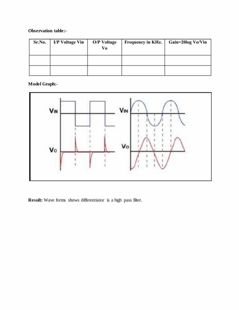
Observation table:-
Model Graph:-
Result: Wave forms shows differentiator is a high pass filter.
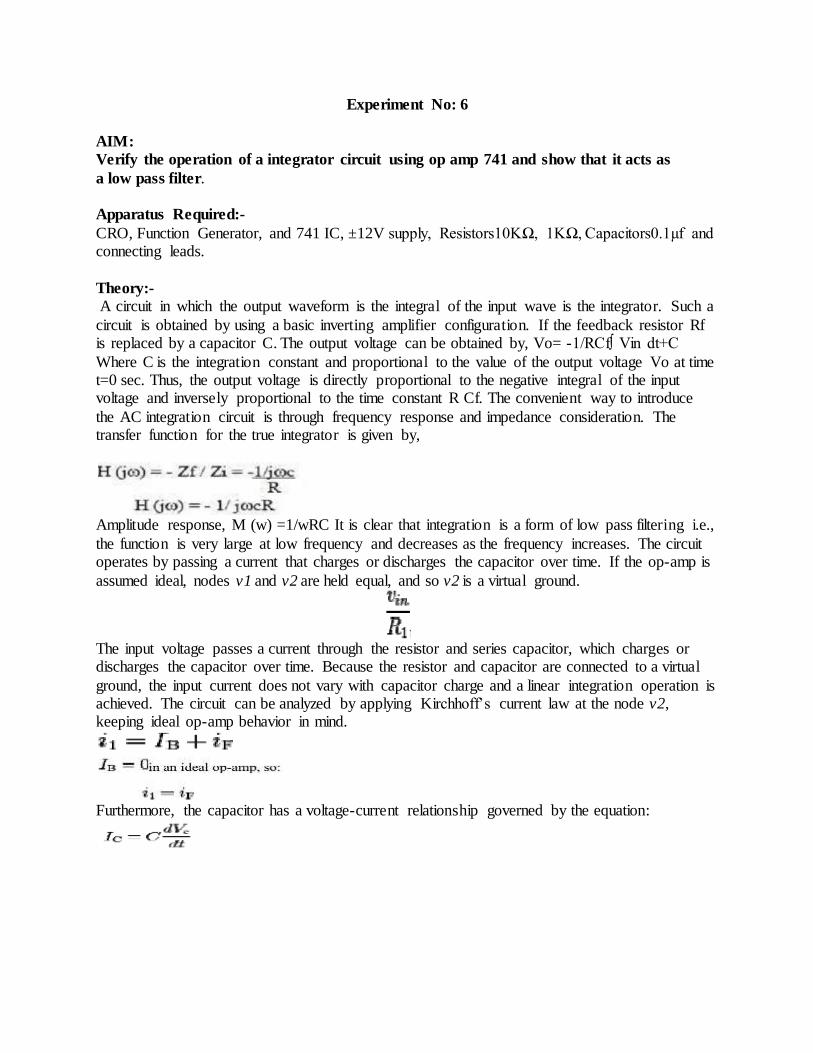
Experiment No: 6
AIM:
Verify the operation of a integrator circuit using op amp 741 and show that it acts as
a low pass filter. Apparatus Required:-
CRO, Function Generator, and 741 IC, ±12V supply, Resistors10KΩ, 1KΩ, Capacitors0.1µf and connecting leads.
Theory:-
A circuit in which the output waveform is the integral of the input wave is the integrator. Such a
circuit is obtained by using a basic inverting amplifier configuration. If the feedback resistor Rf is replaced by a capacitor C. The output voltage can be obtained by, Vo= -1/RCf∫ Vin dt+C
Where C is the integration constant and proportional to the value of the output voltage Vo at time t=0 sec. Thus, the output voltage is directly proportional to the negative integral of the input voltage and inversely proportional to the time constant R Cf. The convenient way to introduce
the AC integration circuit is through frequency response and impedance consideration. The transfer function for the true integrator is given by,
Amplitude response, M (w) =1/wRC It is clear that integration is a form of low pass filtering i.e.,
the function is very large at low frequency and decreases as the frequency increases. The circuit operates by passing a current that charges or discharges the capacitor over time. If the op-amp is
assumed ideal, nodes v1 and v2 are held equal, and so v2 is a virtual ground.
The input voltage passes a current through the resistor and series capacitor, which charges or discharges the capacitor over time. Because the resistor and capacitor are connected to a virtual
ground, the input current does not vary with capacitor charge and a linear integration operation is achieved. The circuit can be analyzed by applying Kirchhoff’s current law at the node v2, keeping ideal op-amp behavior in mind.
Furthermore, the capacitor has a voltage-current relationship governed by the equation:
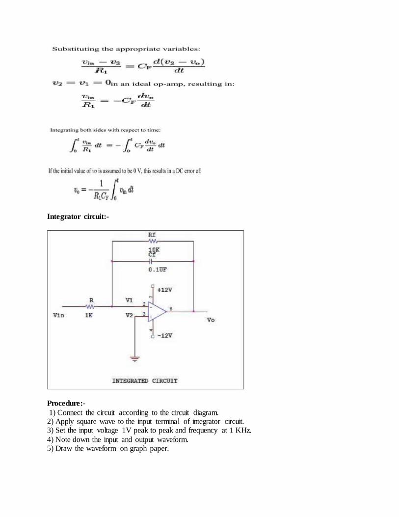
Integrator circuit:-
Procedure:-
1) Connect the circuit according to the circuit diagram. 2) Apply square wave to the input terminal of integrator circuit. 3) Set the input voltage 1V peak to peak and frequency at 1 KHz.
4) Note down the input and output waveform. 5) Draw the waveform on graph paper.
Observation Table:-
Model Output:-
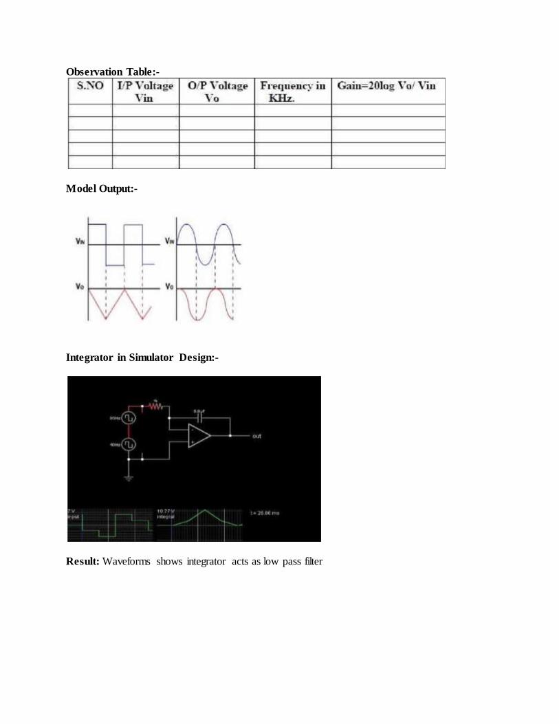
Integrator in Simulator Design:-
Result: Waveforms shows integrator acts as low pass filter
Experiment No: 7
AIM:
Design and verify the operations of op amp adder (summing) and subtractor circuit
Using 741 Op-amp.
Apparatus Required:
CRO, Function Generator, 741 IC, ±12V supply, Resistors, and Connecting leads
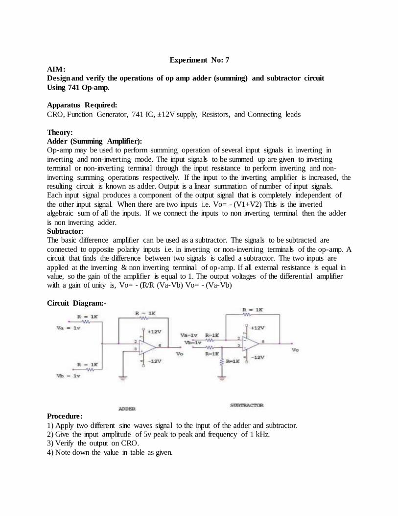
Theory: Adder (Summing Amplifier): Op-amp may be used to perform summing operation of several input signals in inverting in
inverting and non-inverting mode. The input signals to be summed up are given to inverting terminal or non-inverting terminal through the input resistance to perform inverting and non-
inverting summing operations respectively. If the input to the inverting amplifier is increased, the resulting circuit is known as adder. Output is a linear summation of number of input signals. Each input signal produces a component of the output signal that is completely independent of
the other input signal. When there are two inputs i.e. Vo= - (V1+V2) This is the inverted algebraic sum of all the inputs. If we connect the inputs to non inverting terminal then the adder
is non inverting adder. Subtractor:
The basic difference amplifier can be used as a subtractor. The signals to be subtracted are
connected to opposite polarity inputs i.e. in inverting or non-inverting terminals of the op-amp. A circuit that finds the difference between two signals is called a subtractor. The two inputs are
applied at the inverting & non inverting terminal of op-amp. If all external resistance is equal in value, so the gain of the amplifier is equal to 1. The output voltages of the differential amplifier with a gain of unity is, Vo= - (R/R (Va-Vb) Vo= - (Va-Vb)
Circuit Diagram:-
Procedure:
1) Apply two different sine waves signal to the input of the adder and subtractor. 2) Give the input amplitude of 5v peak to peak and frequency of 1 kHz. 3) Verify the output on CRO.
4) Note down the value in table as given.
Observation:-
Adder:-
Subtractor:-
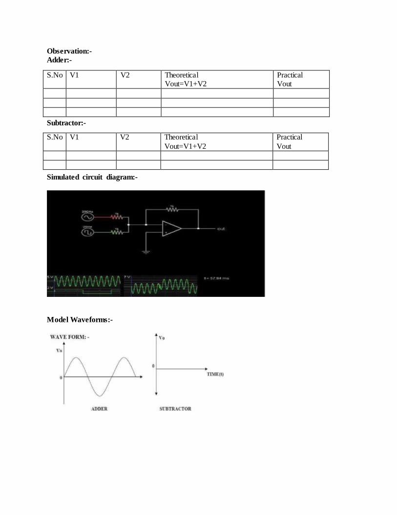
Simulated circuit diagram:-
Model Waveforms:-
S.No V1 V2 Theoretical Vout=V1+V2
Practical Vout
S.No V1 V2 Theoretical
Vout=V1+V2
Practical
Vout
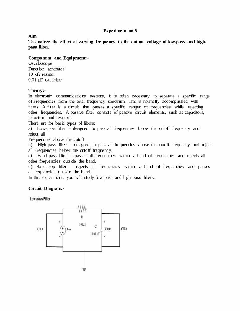
Experiment no 8
Aim
To analyze the effect of varying frequency to the output voltage of low-pass and high-
pass filter.
Component and Equipment:-
Oscilloscope
Function generator 10 kΩ resistor
0.01 µF capacitor Theory:-
In electronic communications systems, it is often necessary to separate a specific range of Frequencies from the total frequency spectrum. This is normally accomplished with
filters. A filter is a circuit that passes a specific ranger of frequencies while rejecting other frequencies. A passive filter consists of passive circuit elements, such as capacitors, inductors and resistors.
There are for basic types of filters: a) Low-pass filter – designed to pass all frequencies below the cutoff frequency and
reject all Frequencies above the cutoff b) High-pass filter – designed to pass all frequencies above the cutoff frequency and reject
all Frequencies below the cutoff frequency. c) Band-pass filter – passes all frequencies within a band of frequencies and rejects all
other frequencies outside the band. d) Band-stop filter – rejects all frequencies within a band of frequencies and passes all frequencies outside the band.
In this experiment, you will study low-pass and high-pass filters.
Circuit Diagram:-
Procedure:-
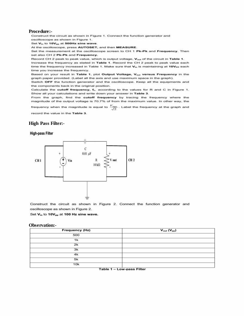
High Pass Filter:-
Observation:-

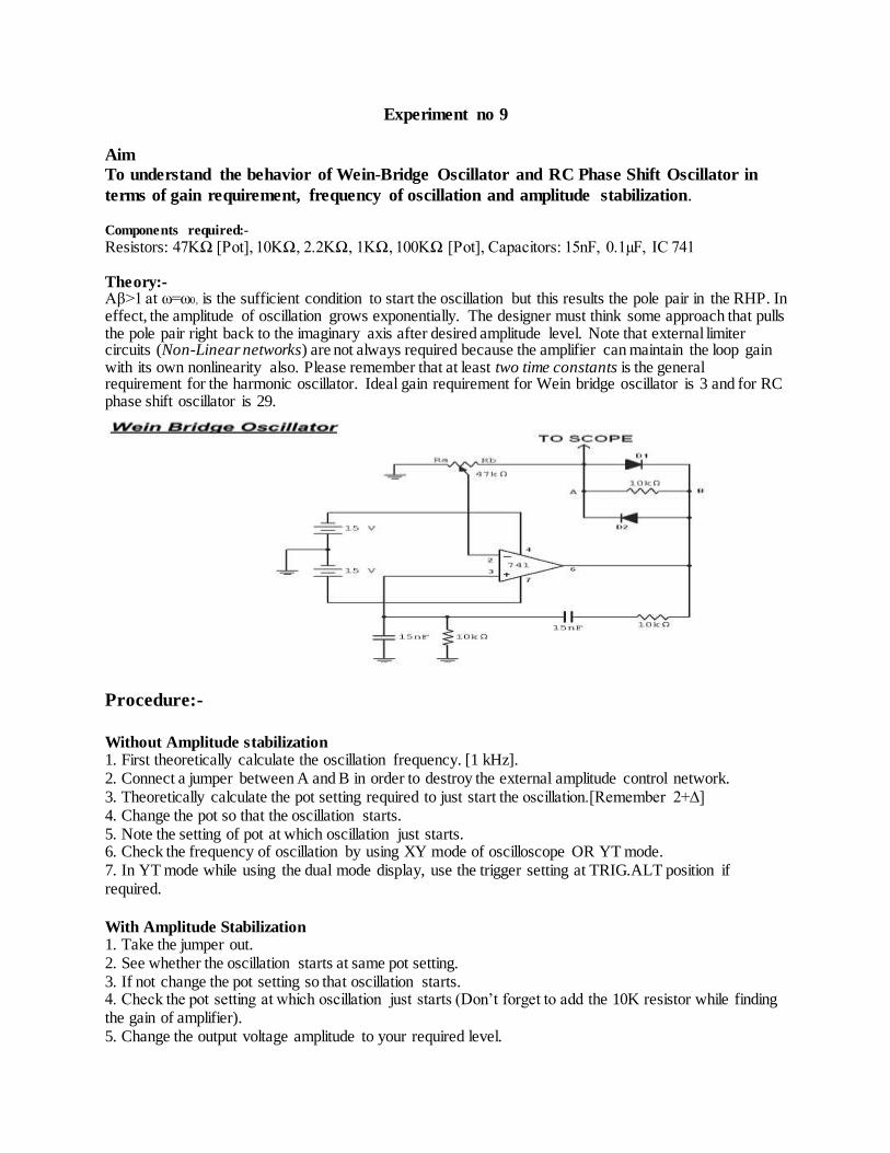
Experiment no 9
Aim
To understand the behavior of Wein-Bridge Oscillator and RC Phase Shift Oscillator in
terms of gain requirement, frequency of oscillation and amplitude stabilization.
Components required:-
Resistors: 47KΩ [Pot], 10KΩ, 2.2KΩ, 1KΩ, 100KΩ [Pot], Capacitors: 15nF, 0.1µF, IC 741
Theory:- Aβ>1 at ω=ω0, is the sufficient condition to start the oscillation but this results the pole pair in the RHP. In effect, the amplitude of oscillation grows exponentially. The designer must think some approach that pulls the pole pair right back to the imaginary axis after desired amplitude level. Note that external limiter circuits (Non-Linear networks) are not always required because the amplifier can maintain the loop gain with its own nonlinearity also. Please remember that at least two time constants is the general requirement for the harmonic oscillator. Ideal gain requirement for Wein bridge oscillator is 3 and for RC phase shift oscillator is 29.
Procedure:-
Without Amplitude stabilization 1. First theoretically calculate the oscillation frequency. [1 kHz]. 2. Connect a jumper between A and B in order to destroy the external amplitude control network. 3. Theoretically calculate the pot setting required to just start the oscillation.[Remember 2+∆] 4. Change the pot so that the oscillation starts. 5. Note the setting of pot at which oscillation just starts. 6. Check the frequency of oscillation by using XY mode of oscilloscope OR YT mode. 7. In YT mode while using the dual mode display, use the trigger setting at TRIG.ALT position if required.
With Amplitude Stabilization 1. Take the jumper out. 2. See whether the oscillation starts at same pot setting. 3. If not change the pot setting so that oscillation starts. 4. Check the pot setting at which oscillation just starts (Don’t forget to add the 10K resistor while finding the gain of amplifier). 5. Change the output voltage amplitude to your required level.
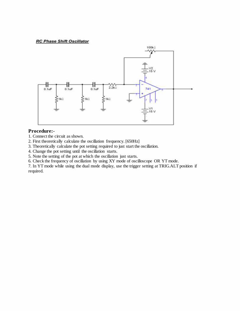
Procedure:- 1. Connect the circuit as shown. 2. First theoretically calculate the oscillation frequency. [650Hz] 3. Theoretically calculate the pot setting required to just start the oscillation. 4. Change the pot setting until the oscillation starts. 5. Note the setting of the pot at which the oscillation just starts. 6. Check the frequency of oscillation by using XY mode of oscilloscope OR YT mode. 7. In YT mode while using the dual mode display, use the trigger setting at TRIG.ALT position if required.