Embed Size (px)
DESCRIPTION
Solucionario Teoria de Circuitos y dispositivos electrnicos 10 ed. Boylestad Nashelsky
Citation preview
Instructor’s Resource Manual to accompany
Electronic Devices and Circuit Theory
Tenth Edition
Robert L. Boylestad Louis Nashelsky
Upper Saddle River, New Jersey Columbus, Ohio

Copyright © 2009 by Pearson Education, Inc., Upper Saddle River, New Jersey 07458. Pearson Prentice Hall. All rights reserved. Printed in the United States of America. This publication is protected by Copyright and permission should be obtained from the publisher prior to any prohibited reproduction, storage in a retrieval system, or transmission in any form or by any means, electronic, mechanical, photocopying, recording, or likewise. For information regarding permission(s), write to: Rights and Permissions Department. Pearson Prentice Hall™ is a trademark of Pearson Education, Inc. Pearson® is a registered trademark of Pearson plc Prentice Hall® is a registered trademark of Pearson Education, Inc. Instructors of classes using Boylestad/Nashelsky, Electronic Devices and Circuit Theory, 10th edition, may reproduce material from the instructor’s text solutions manual for classroom use.
10 9 8 7 6 5 4 3 2 1
ISBN-13: 978-0-13-503865-9 ISBN-10: 0-13-503865-0
iii
Contents
Solutions to Problems in Text 1 Solutions for Laboratory Manual 185
1
Chapter 1 1. Copper has 20 orbiting electrons with only one electron in the outermost shell. The fact that
the outermost shell with its 29th electron is incomplete (subshell can contain 2 electrons) and distant from the nucleus reveals that this electron is loosely bound to its parent atom. The application of an external electric field of the correct polarity can easily draw this loosely bound electron from its atomic structure for conduction.
Both intrinsic silicon and germanium have complete outer shells due to the sharing (covalent
bonding) of electrons between atoms. Electrons that are part of a complete shell structure require increased levels of applied attractive forces to be removed from their parent atom.
2. Intrinsic material: an intrinsic semiconductor is one that has been refined to be as pure as
physically possible. That is, one with the fewest possible number of impurities. Negative temperature coefficient: materials with negative temperature coefficients have
decreasing resistance levels as the temperature increases. Covalent bonding: covalent bonding is the sharing of electrons between neighboring atoms to
form complete outermost shells and a more stable lattice structure. 3. − 4. W = QV = (6 C)(3 V) = 18 J 5. 48 eV = 48(1.6 × 10⁻¹⁹ J) = 76.8 × 10⁻¹⁹ J
Q = WV
= 1976.8 10 J
12 V
−× = 6.40 × 10⁻¹⁹ C
6.4 × 10⁻¹⁹ C is the charge associated with 4 electrons. 6. GaP Gallium Phosphide Eg = 2.24 eV ZnS Zinc Sulfide Eg = 3.67 eV 7. An n-type semiconductor material has an excess of electrons for conduction established by
doping an intrinsic material with donor atoms having more valence electrons than needed to establish the covalent bonding. The majority carrier is the electron while the minority carrier is the hole.
A p-type semiconductor material is formed by doping an intrinsic material with acceptor
atoms having an insufficient number of electrons in the valence shell to complete the covalent bonding thereby creating a hole in the covalent structure. The majority carrier is the hole while the minority carrier is the electron.
8. A donor atom has five electrons in its outermost valence shell while an acceptor atom has
only 3 electrons in the valence shell. 9. Majority carriers are those carriers of a material that far exceed the number of any other
carriers in the material. Minority carriers are those carriers of a material that are less in number than any other carrier
of the material.
2
10. Same basic appearance as Fig. 1.7 since arsenic also has 5 valence electrons (pentavalent). 11. Same basic appearance as Fig. 1.9 since boron also has 3 valence electrons (trivalent). 12. − 13. − 14. For forward bias, the positive potential is applied to the p-type material and the negative
potential to the n-type material. 15. TK = 20 + 273 = 293 k = 11,600/n = 11,600/2 (low value of VD) = 5800
ID = Is 1D
K
kVTe
⎛ ⎞−⎜ ⎟⎜ ⎟
⎝ ⎠ = 50 × 10−9
(5800)(0.6)293 1e
⎛ ⎞−⎜ ⎟
⎝ ⎠
= 50 × 10−9 (e11.877 − 1) = 7.197 mA
16. k = 11,600/n = 11,600/2 = 5800 (n = 2 for VD = 0.6 V) TK = TC + 273 = 100 + 273 = 373
(5800)(0.6 V)
/ 9.33373KkV Te e e= = = 11.27 × 10³ I = /( 1)KkV T
sI e − = 5 μA(11.27 × 10³ − 1) = 56.35 mA 17. (a) TK = 20 + 273 = 293 k = 11,600/n = 11,600/2 = 5800
ID = Is 1D
K
kVTe
⎛ ⎞−⎜ ⎟⎜ ⎟
⎝ ⎠ = 0.1μA
(5800)( 10 V)293 1e−⎛ ⎞
−⎜ ⎟⎝ ⎠
= 0.1 × 10⁻⁶(e−197.95 − 1) = 0.1 × 10⁻⁶(1.07 × 10−86 − 1) ≅ 0.1 × 10⁻⁶ 0.1μA ID = Is = 0.1 μA
(b) The result is expected since the diode current under reverse-bias conditions should equal the saturation value.
18. (a)
x y = ex 0 1 1 2.7182 2 7.389 3 20.086 4 54.6 5 148.4
(b) y = e0 = 1 (c) For V = 0 V, e0 = 1 and I = Is(1 − 1) = 0 mA
3
19. T = 20°C: Is = 0.1 μA T = 30°C: Is = 2(0.1 μA) = 0.2 μA (Doubles every 10°C rise in temperature) T = 40°C: Is = 2(0.2 μA) = 0.4 μA T = 50°C: Is = 2(0.4 μA) = 0.8 μA T = 60°C: Is = 2(0.8 μA) = 1.6 μA
1.6 μA: 0.1 μA ⇒ 16:1 increase due to rise in temperature of 40°C. 20. For most applications the silicon diode is the device of choice due to its higher temperature
capability. Ge typically has a working limit of about 85 degrees centigrade while Si can be used at temperatures approaching 200 degrees centigrade. Silicon diodes also have a higher current handling capability. Germanium diodes are the better device for some RF small signal applications, where the smaller threshold voltage may prove advantageous.
21. From 1.19:
−75°C 25°C 125°C VF @ 10 mA Is
1.1 V 0.01 pA
0.85 V 1 pA
0.6 V 1.05 μA
VF decreased with increase in temperature 1.1 V: 0.6 V ≅ 1.83:1 Is increased with increase in temperature 1.05 μA: 0.01 pA = 105 × 103:1 22. An “ideal” device or system is one that has the characteristics we would prefer to have when
using a device or system in a practical application. Usually, however, technology only permits a close replica of the desired characteristics. The “ideal” characteristics provide an excellent basis for comparison with the actual device characteristics permitting an estimate of how well the device or system will perform. On occasion, the “ideal” device or system can be assumed to obtain a good estimate of the overall response of the design. When assuming an “ideal” device or system there is no regard for component or manufacturing tolerances or any variation from device to device of a particular lot.
23. In the forward-bias region the 0 V drop across the diode at any level of current results in a
resistance level of zero ohms – the “on” state – conduction is established. In the reverse-bias region the zero current level at any reverse-bias voltage assures a very high resistance level − the open circuit or “off” state − conduction is interrupted.
24. The most important difference between the characteristics of a diode and a simple switch is
that the switch, being mechanical, is capable of conducting current in either direction while the diode only allows charge to flow through the element in one direction (specifically the direction defined by the arrow of the symbol using conventional current flow).
25. VD ≅ 0.66 V, ID = 2 mA
RDC = 0.65 V2 mA
D
D
VI
= = 325 Ω
4
26. At ID = 15 mA, VD = 0.82 V
RDC = 0.82 V15 mA
D
D
VI
= = 54.67 Ω
As the forward diode current increases, the static resistance decreases. 27. VD = −10 V, ID = Is = −0.1 μA
RDC = 10 V0.1 A
D
D
VI μ
= = 100 MΩ
VD = −30 V, ID = Is= −0.1 μA
RDC = 30 V0.1 A
D
D
VI μ
= = 300 MΩ
As the reverse voltage increases, the reverse resistance increases directly (since the diode
leakage current remains constant).
28. (a) rd = 0.79 V 0.76 V 0.03 V15 mA 5 mA 10 mA
d
d
VI
Δ −= =
Δ − = 3 Ω
(b) rd = 26 mV 26 mV10 mADI
= = 2.6 Ω
(c) quite close 29. ID = 10 mA, VD = 0.76 V
RDC = 0.76 V10 mA
D
D
VI
= = 76 Ω
rd = 0.79 V 0.76 V 0.03 V15 mA 5 mA 10 mA
d
d
VI
Δ −≅ =
Δ − = 3 Ω
RDC >> rd
30. ID = 1 mA, rd = 0.72 V 0.61 V2 mA 0 mA
d
d
VI
Δ −=
Δ − = 55 Ω
ID = 15 mA, rd = 0.8 V 0.78 V20 mA 10 mA
d
d
VI
Δ −=
Δ − = 2 Ω
31. ID = 1 mA, rd = 26 mV2DI
⎛ ⎞⎜ ⎟⎝ ⎠
= 2(26 Ω) = 52 Ω vs 55 Ω (#30)
ID = 15 mA, rd = 26 mV 26 mV15 mADI
= = 1.73 Ω vs 2 Ω (#30)
32. rav = 0.9 V 0.6 V13.5 mA 1.2 mA
d
d
VI
Δ −=
Δ − = 24.4 Ω
5
33. rd = 0.8 V 0.7 V 0.09 V7 mA 3 mA 4 mA
d
d
VI
Δ −≅ =
Δ − = 22.5 Ω
(relatively close to average value of 24.4 Ω (#32))
34. rav = 0.9 V 0.7 V 0.2 V14 mA 0 mA 14 mA
d
d
VI
Δ −= =
Δ − = 14.29 Ω
35. Using the best approximation to the curve beyond VD = 0.7 V:
rav = 0.8 V 0.7 V 0.1 V25 mA 0 mA 25 mA
d
d
VI
Δ −≅ =
Δ − = 4 Ω
36. (a) VR = −25 V: CT ≅ 0.75 pF VR = −10 V: CT ≅ 1.25 pF
1.25 pF 0.75 pF 0.5 pF10 V 25 V 15 V
T
R
CV
Δ −= =
Δ − = 0.033 pF/V
(b) VR = −10 V: CT ≅ 1.25 pF VR = −1 V: CT ≅ 3 pF
1.25 pF 3 pF 1.75 pF10 V 1 V 9 V
T
R
CV
Δ −= =
Δ − = 0.194 pF/V
(c) 0.194 pF/V: 0.033 pF/V = 5.88:1 ≅ 6:1 Increased sensitivity near VD = 0 V 37. From Fig. 1.33 VD = 0 V, CD = 3.3 pF VD = 0.25 V, CD = 9 pF 38. The transition capacitance is due to the depletion region acting like a dielectric in the reverse-
bias region, while the diffusion capacitance is determined by the rate of charge injection into the region just outside the depletion boundaries of a forward-biased device. Both capacitances are present in both the reverse- and forward-bias directions, but the transition capacitance is the dominant effect for reverse-biased diodes and the diffusion capacitance is the dominant effect for forward-biased conditions.
6
39. VD = 0.2 V, CD = 7.3 pF
XC = 1 12 2 (6 MHz)(7.3 pF)fCπ π
= = 3.64 kΩ
VD = −20 V, CT = 0.9 pF
XC = 1 12 2 (6 MHz)(0.9 pF)fCπ π
= = 29.47 kΩ
40. If = 10 V10 kΩ
= 1 mA
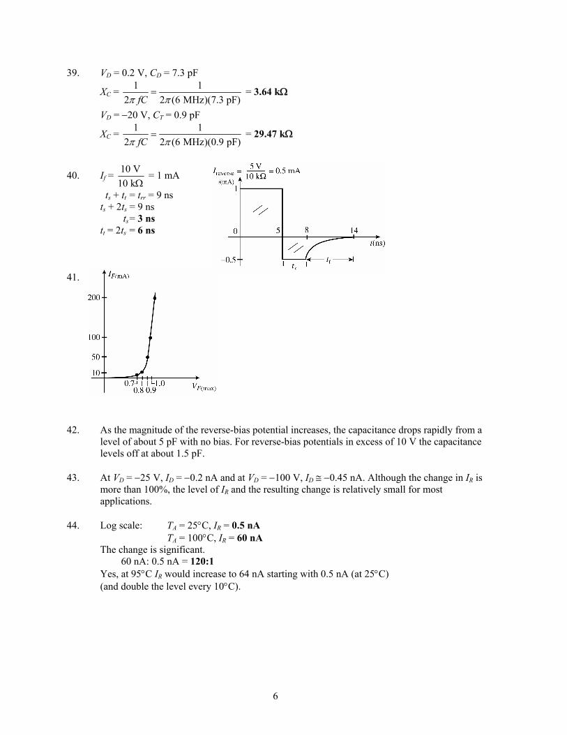
ts + tt = trr = 9 ns ts + 2ts = 9 ns ts = 3 ns tt = 2ts = 6 ns 41. 42. As the magnitude of the reverse-bias potential increases, the capacitance drops rapidly from a
level of about 5 pF with no bias. For reverse-bias potentials in excess of 10 V the capacitance levels off at about 1.5 pF.
43. At VD = −25 V, ID = −0.2 nA and at VD = −100 V, ID ≅ −0.45 nA. Although the change in IR is
more than 100%, the level of IR and the resulting change is relatively small for most applications.
44. Log scale: TA = 25°C, IR = 0.5 nA TA = 100°C, IR = 60 nA The change is significant. 60 nA: 0.5 nA = 120:1 Yes, at 95°C IR would increase to 64 nA starting with 0.5 nA (at 25°C) (and double the level every 10°C).
7
45. IF = 0.1 mA: rd ≅ 700 Ω IF = 1.5 mA: rd ≅ 70 Ω IF = 20 mA: rd ≅ 6 Ω The results support the fact that the dynamic or ac resistance decreases rapidly with
increasing current levels. 46. T = 25°C: Pmax = 500 mW T = 100°C: Pmax = 260 mW Pmax = VFIF
IF = max 500 mW0.7 VF
PV
= = 714.29 mA
IF = max 260 mW0.7 VF
PV
= = 371.43 mA
714.29 mA: 371.43 mA = 1.92:1 ≅ 2:1 47. Using the bottom right graph of Fig. 1.37: IF = 500 mA @ T = 25°C At IF = 250 mA, T ≅ 104°C 48.
49. TC = +0.072% = 1 0
100%( )
Z
Z
VV T T
Δ×
−
0.072 = 1
0.75 V 10010 V( 25)T
×−
0.072 = 1
7.525T −
T1 − 25° = 7.50.072
= 104.17°
T1 = 104.17° + 25° = 129.17°
50. TC = 1 0( )
Z
Z
VV T T
Δ−
× 100%
= (5 V 4.8 V)5 V(100 25 )
−° − °
× 100% = 0.053%/°C
8
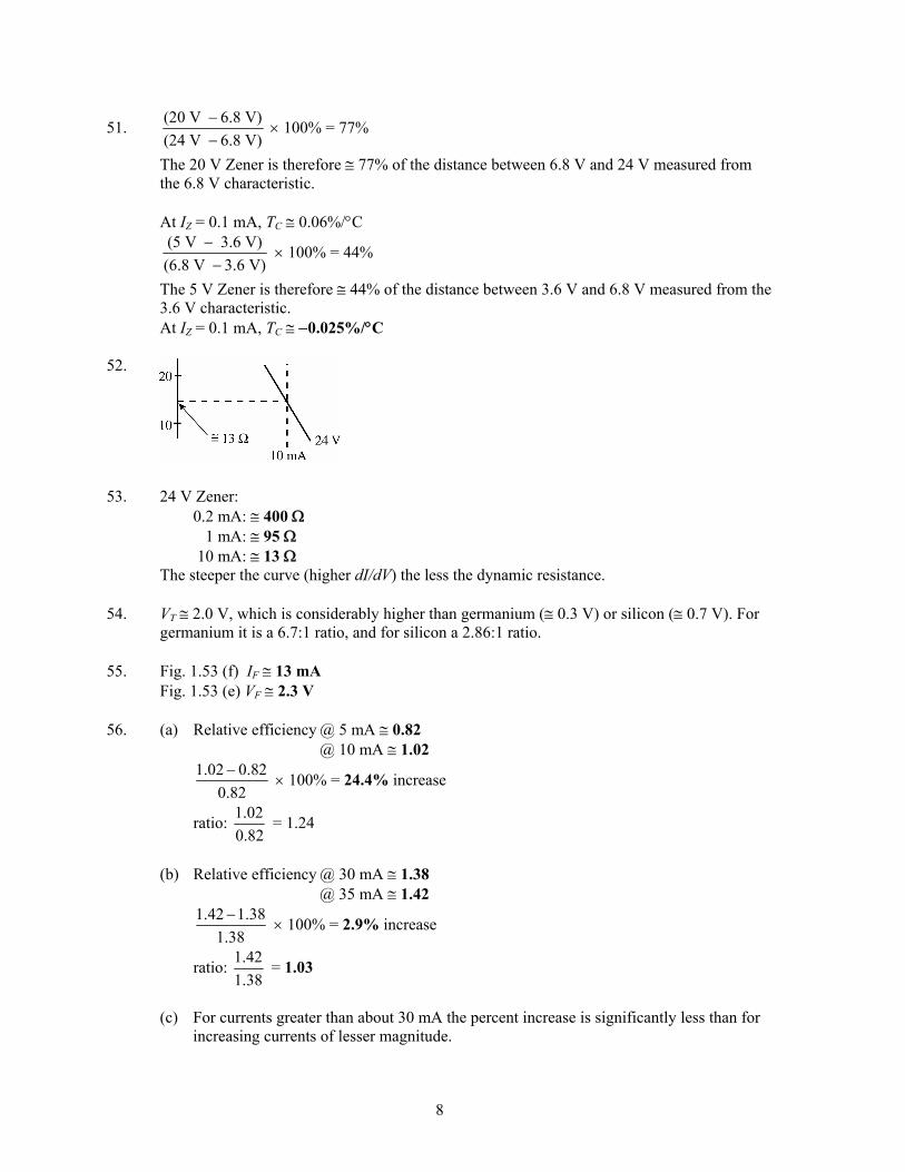
51. (20 V 6.8 V)(24 V 6.8 V)
−−
× 100% = 77%
The 20 V Zener is therefore ≅ 77% of the distance between 6.8 V and 24 V measured from the 6.8 V characteristic.
At IZ = 0.1 mA, TC ≅ 0.06%/°C
(5 V 3.6 V)(6.8 V 3.6 V)
−−
× 100% = 44%
The 5 V Zener is therefore ≅ 44% of the distance between 3.6 V and 6.8 V measured from the 3.6 V characteristic.
At IZ = 0.1 mA, TC ≅ −0.025%/°C 52. 53. 24 V Zener: 0.2 mA: ≅ 400 Ω 1 mA: ≅ 95 Ω 10 mA: ≅ 13 Ω The steeper the curve (higher dI/dV) the less the dynamic resistance. 54. VT ≅ 2.0 V, which is considerably higher than germanium (≅ 0.3 V) or silicon (≅ 0.7 V). For
germanium it is a 6.7:1 ratio, and for silicon a 2.86:1 ratio. 55. Fig. 1.53 (f) IF ≅ 13 mA Fig. 1.53 (e) VF ≅ 2.3 V 56. (a) Relative efficiency @ 5 mA ≅ 0.82 @ 10 mA ≅ 1.02
1.02 0.820.82− × 100% = 24.4% increase
ratio: 1.020.82
= 1.24
(b) Relative efficiency @ 30 mA ≅ 1.38 @ 35 mA ≅ 1.42
1.42 1.381.38− × 100% = 2.9% increase
ratio: 1.421.38
= 1.03
(c) For currents greater than about 30 mA the percent increase is significantly less than for
increasing currents of lesser magnitude.
9
57. (a) 0.753.0
= 0.25
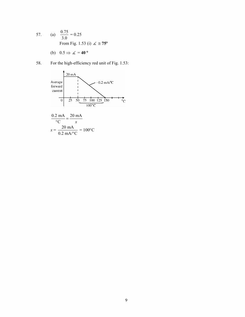
From Fig. 1.53 (i) ≅ 75° (b) 0.5 ⇒ = 40 ° 58. For the high-efficiency red unit of Fig. 1.53:
0.2 mA 20 mAC x
=°
x = 20 mA0.2 mA/ C°
= 100°C
10
Chapter 2
1. The load line will intersect at ID = 8 V330
ER=
Ω = 24.24 mA and VD = 8 V.
(a)
QDV ≅ 0.92 V
QDI ≅ 21.5 mA
VR = E − QDV = 8 V − 0.92 V = 7.08 V
(b) QDV ≅ 0.7 V
QDI ≅ 22.2 mA
VR = E − QDV = 8 V − 0.7 V = 7.3 V
(c) QDV ≅ 0 V
QDI ≅ 24.24 mA
VR = E − QDV = 8 V − 0 V = 8 V
For (a) and (b), levels of QDV and
QDI are quite close. Levels of part (c) are reasonably close but as expected due to level of applied voltage E.
2. (a) ID = 5 V2.2 k
ER=
Ω = 2.27 mA
The load line extends from ID = 2.27 mA to VD = 5 V.
QDV ≅ 0.7 V, QDI ≅ 2 mA
(b) ID = 5 V0.47 k
ER=
Ω = 10.64 mA
The load line extends from ID = 10.64 mA to VD = 5 V.
QDV ≅ 0.8 V, QDI ≅ 9 mA
(c) ID = 5 V0.18 k
ER=
Ω = 27.78 mA
The load line extends from ID = 27.78 mA to VD = 5 V.
QDV ≅ 0.93 V, QDI ≅ 22.5 mA
The resulting values of
QDV are quite close, while QDI extends from 2 mA to 22.5 mA.
3. Load line through
QDI = 10 mA of characteristics and VD = 7 V will intersect ID axis as 11.25 mA.
ID = 11.25 mA = 7 VER R=
with R = 7 V11.25 mA
= 0.62 kΩ
11
4. (a) ID = IR = 30 V 0.7 V2.2 k
DE VR− −
=Ω
= 13.32 mA
VD = 0.7 V, VR = E − VD = 30 V − 0.7 V = 29.3 V
(b) ID = 30 V 0 V2.2 k
DE VR− −
=Ω
= 13.64 mA
VD = 0 V, VR = 30 V Yes, since E VT the levels of ID and VR are quite close. 5. (a) I = 0 mA; diode reverse-biased. (b) V20Ω = 20 V − 0.7 V = 19.3 V (Kirchhoff’s voltage law)
I = 19.3 V20 Ω
= 0.965 A
(c) I = 10 V10Ω
= 1 A; center branch open
6. (a) Diode forward-biased, Kirchhoff’s voltage law (CW): −5 V + 0.7 V − Vo = 0 Vo = −4.3 V
IR = ID = 4.3 V2.2 k
oVR
=Ω
= 1.955 mA
(b) Diode forward-biased,
ID = 8 V 0.7 V1.2 k 4.7 k
−Ω + Ω
= 1.24 mA
Vo = V4.7 kΩ + VD = (1.24 mA)(4.7 kΩ) + 0.7 V = 6.53 V
7. (a) Vo = 2 k (20 V 0.7 V 0.3V)2 k 2 k
Ω − −Ω + Ω
= 12
(20 V – 1 V) = 12
(19 V) = 9.5 V
(b) I = 10 V 2V 0.7 V) 11.3 V1.2 k 4.7 k 5.9 k
+ −=
Ω + Ω Ω = 1.915 mA
V ′ = IR = (1.915 mA)(4.7 kΩ) = 9 V Vo = V ′ − 2 V = 9 V − 2 V = 7 V
12
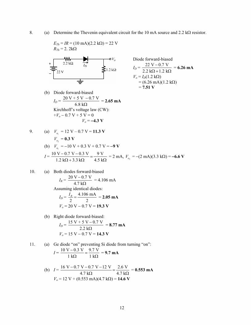
8. (a) Determine the Thevenin equivalent circuit for the 10 mA source and 2.2 kΩ resistor. ETh = IR = (10 mA)(2.2 kΩ) = 22 V RTh = 2. 2kΩ Diode forward-biased
ID = 22 V 0.7 V2.2 k 1.2 k
−Ω + Ω
= 6.26 mA
Vo = ID(1.2 kΩ) = (6.26 mA)(1.2 kΩ) = 7.51 V (b) Diode forward-biased
ID = 20 V + 5 V 0.7 V6.8 k
−Ω
= 2.65 mA
Kirchhoff’s voltage law (CW): +Vo − 0.7 V + 5 V = 0 Vo = −4.3 V 9. (a)
1oV = 12 V – 0.7 V = 11.3 V
2oV = 0.3 V (b)
1oV = −10 V + 0.3 V + 0.7 V = −9 V
I = 10 V 0.7 V 0.3 V 9 V1.2 k 3.3 k 4.5 k
− −=
Ω + Ω Ω = 2 mA,
2oV = −(2 mA)(3.3 kΩ) = −6.6 V
10. (a) Both diodes forward-biased
IR = 20 V 0.7 V4.7 k−Ω
= 4.106 mA
Assuming identical diodes:
ID = 4.106 mA2 2RI= = 2.05 mA
Vo = 20 V − 0.7 V = 19.3 V (b) Right diode forward-biased:
ID = 15 V + 5 V 0.7 V2.2 k
−Ω
= 8.77 mA
Vo = 15 V − 0.7 V = 14.3 V 11. (a) Ge diode “on” preventing Si diode from turning “on”:
I = 10 V 0.3 V 9.7 V1 k 1 k−
=Ω Ω
= 9.7 mA
(b) I = 16 V 0.7 V 0.7 V 12 V 2.6 V4.7 k 4.7 k
− − −=
Ω Ω = 0.553 mA
Vo = 12 V + (0.553 mA)(4.7 kΩ) = 14.6 V
13
12. Both diodes forward-biased:
1oV = 0.7 V, 2oV = 0.3 V
I1 kΩ = 20 V 0.7 V1 k−Ω
= 19.3 V1 kΩ
= 19.3 mA
I0.47 kΩ = 0.7 V 0.3 V0.47 k
−Ω
= 0.851 mA
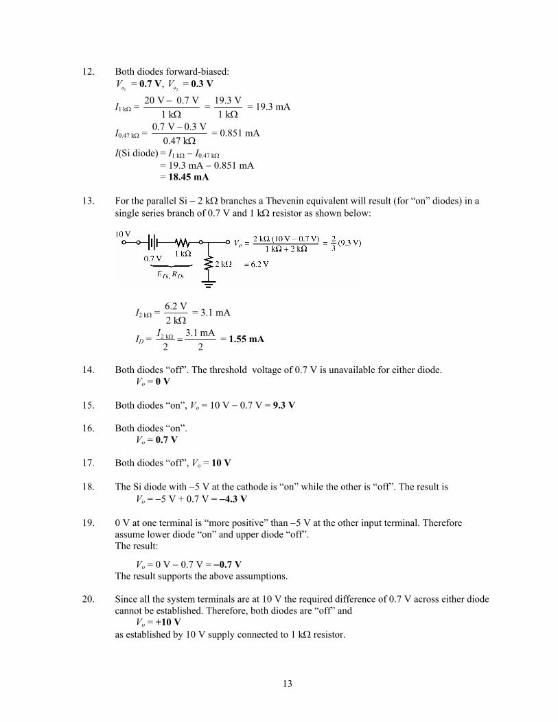
I(Si diode) = I1 kΩ − I0.47 kΩ = 19.3 mA − 0.851 mA = 18.45 mA 13. For the parallel Si − 2 kΩ branches a Thevenin equivalent will result (for “on” diodes) in a
single series branch of 0.7 V and 1 kΩ resistor as shown below:
I2 kΩ = 6.2 V2 kΩ
= 3.1 mA
ID = 2 k 3.1 mA2 2
I Ω = = 1.55 mA
14. Both diodes “off”. The threshold voltage of 0.7 V is unavailable for either diode. Vo = 0 V 15. Both diodes “on”, Vo = 10 V − 0.7 V = 9.3 V 16. Both diodes “on”. Vo = 0.7 V 17. Both diodes “off”, Vo = 10 V 18. The Si diode with −5 V at the cathode is “on” while the other is “off”. The result is Vo = −5 V + 0.7 V = −4.3 V 19. 0 V at one terminal is “more positive” than −5 V at the other input terminal. Therefore
assume lower diode “on” and upper diode “off”. The result:
Vo = 0 V − 0.7 V = −0.7 V The result supports the above assumptions. 20. Since all the system terminals are at 10 V the required difference of 0.7 V across either diode
cannot be established. Therefore, both diodes are “off” and Vo = +10 V as established by 10 V supply connected to 1 kΩ resistor.
14
21. The Si diode requires more terminal voltage than the Ge diode to turn “on”. Therefore, with 5 V at both input terminals, assume Si diode “off” and Ge diode “on”. The result: Vo = 5 V − 0.3 V = 4.7 V The result supports the above assumptions.
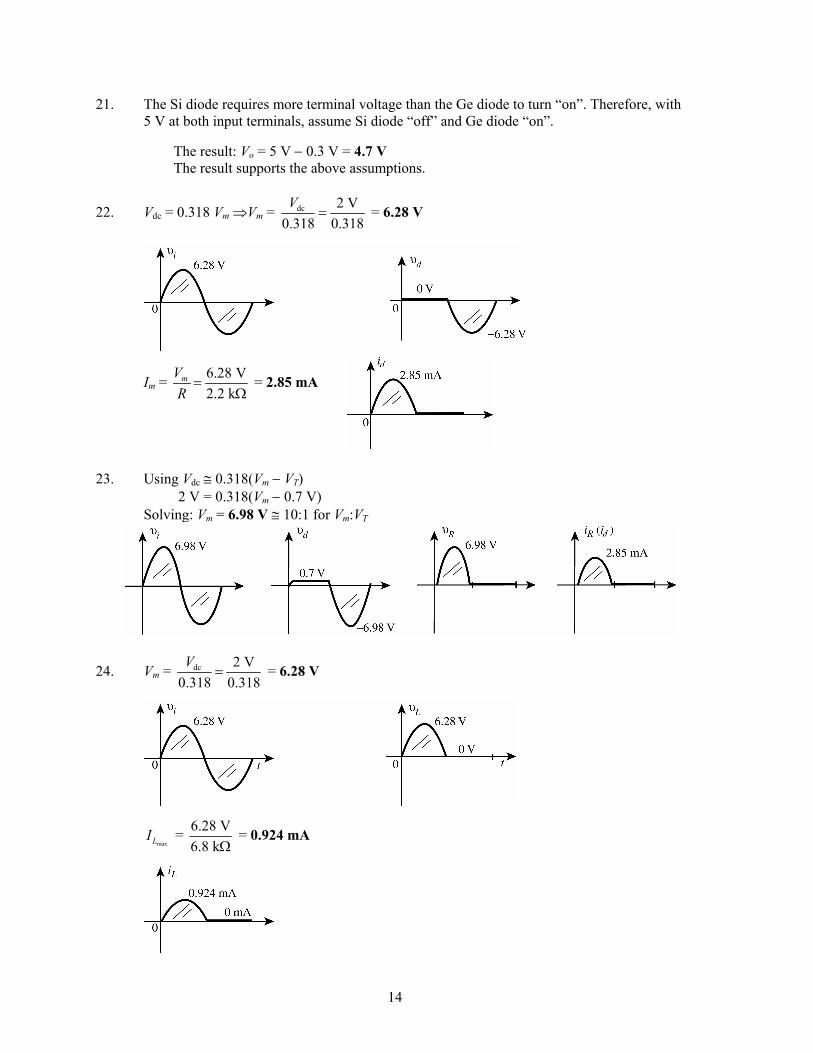
22. Vdc = 0.318 Vm ⇒Vm = dc 2 V0.318 0.318V
= = 6.28 V
Im = 6.28 V2.2 k
mVR
=Ω
= 2.85 mA
23. Using Vdc ≅ 0.318(Vm − VT) 2 V = 0.318(Vm − 0.7 V) Solving: Vm = 6.98 V ≅ 10:1 for Vm:VT
24. Vm = dc 2 V0.318 0.318V
= = 6.28 V
maxLI = 6.28 V
6.8 kΩ = 0.924 mA
15
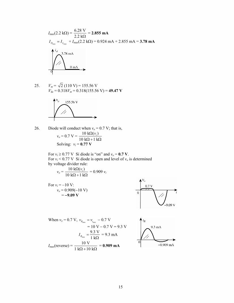
Imax(2.2 kΩ) = 6.28 V2.2 kΩ
= 2.855 mA
max maxD LI I= + Imax(2.2 kΩ) = 0.924 mA + 2.855 mA = 3.78 mA
25. Vm = 2 (110 V) = 155.56 V Vdc = 0.318Vm = 0.318(155.56 V) = 49.47 V
26. Diode will conduct when vo = 0.7 V; that is,
vo = 0.7 V = 10 k ( )10 k 1 k
ivΩΩ+ Ω
Solving: vi = 0.77 V For vi ≥ 0.77 V Si diode is “on” and vo = 0.7 V. For vi < 0.77 V Si diode is open and level of vo is determined by voltage divider rule:
vo = 10 k ( )10 k 1 k
ivΩΩ+ Ω
= 0.909 vi
For vi = −10 V: vo = 0.909(−10 V) = −9.09 V When vo = 0.7 V,
max maxR iv v= − 0.7 V = 10 V − 0.7 V = 9.3 V
max
9.3 V1 kRI =
Ω = 9.3 mA
Imax(reverse) = 10 V1 k 10 kΩ+ Ω
= 0.909 mA
16
27. (a) Pmax = 14 mW = (0.7 V)ID
ID = 14 mW0.7 V
= 20 mA
(b) 4.7 kΩ || 56 kΩ = 4.34 kΩ VR = 160 V − 0.7 V = 159.3 V
Imax = 159.3 V4.34 kΩ
= 36.71 mA
(c) Idiode = max 36.71 mA2 2
I= = 18.36 mA
(d) Yes, ID = 20 mA > 18.36 mA (e) Idiode = 36.71 mA Imax = 20 mA 28. (a) Vm = 2 (120 V) = 169.7 V
mLV = mi
V − 2VD = 169.7 V − 2(0.7 V) = 169.7 V − 1.4 V = 168.3 V Vdc = 0.636(168.3 V) = 107.04 V (b) PIV = Vm(load) + VD = 168.3 V + 0.7 V = 169 V
(c) ID(max) = 168.3 V1 k
mL
L
VR
=Ω
= 168.3 mA
(d) Pmax = VDID = (0.7 V)Imax = (0.7 V)(168.3 mA) = 117.81 mW 29.
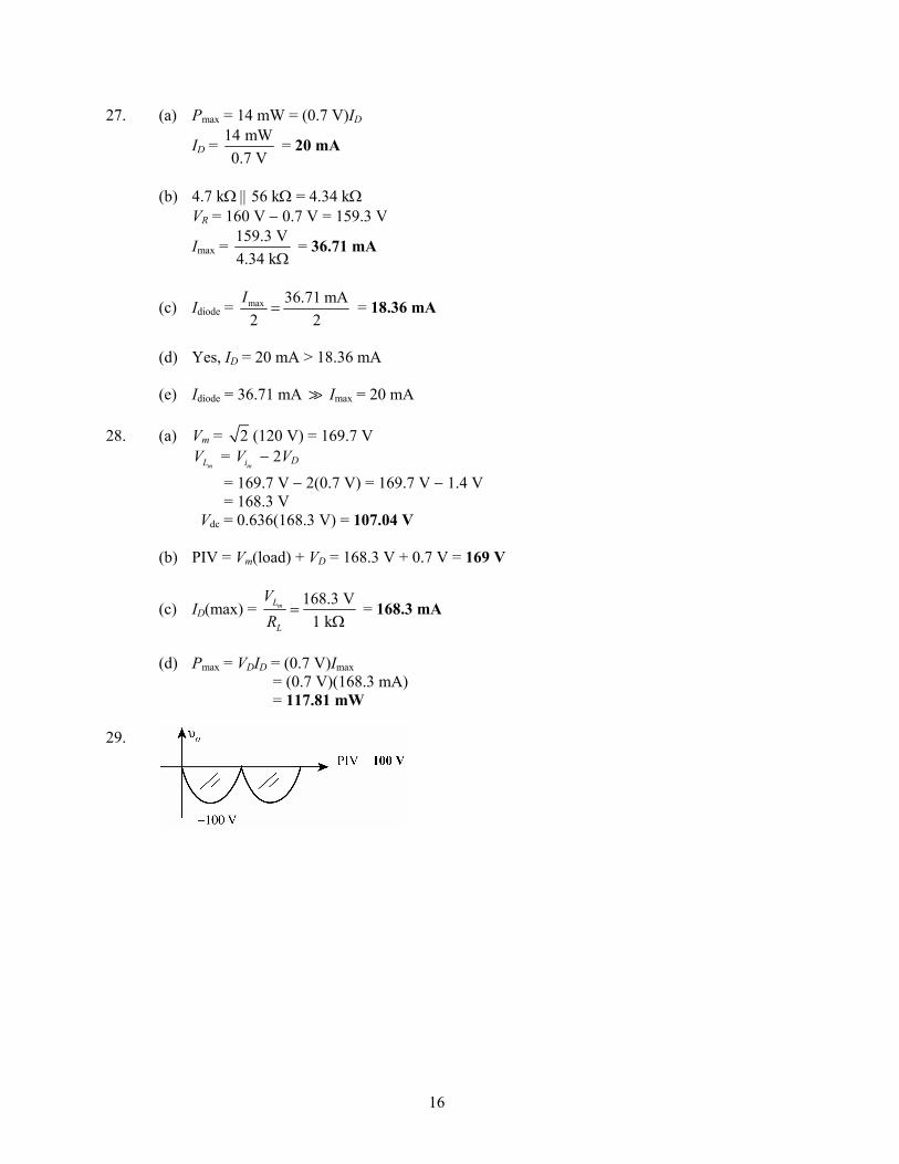
17
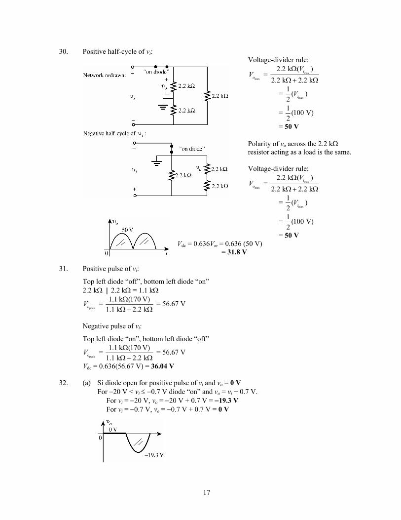
30. Positive half-cycle of vi: Voltage-divider rule:
maxoV = max
2.2 k ( )2.2 k 2.2 k
iVΩ
Ω+ Ω
= max
1 ( )2 iV
= 1 (100 V)2
= 50 V Polarity of vo across the 2.2 kΩ resistor acting as a load is the same. Voltage-divider rule:
maxoV = max
2.2 k ( )2.2 k 2.2 k
iVΩ
Ω+ Ω
= max
1 ( )2 iV
= 1 (100 V)2
= 50 V Vdc = 0.636Vm = 0.636 (50 V) = 31.8 V 31. Positive pulse of vi:
Top left diode “off”, bottom left diode “on” 2.2 kΩ || 2.2 kΩ = 1.1 kΩ
peakoV = 1.1 k (170 V)
1.1 k 2.2 kΩΩ+ Ω
= 56.67 V
Negative pulse of vi:
Top left diode “on”, bottom left diode “off”
peakoV = 1.1 k (170 V)
1.1 k 2.2 kΩΩ+ Ω
= 56.67 V
Vdc = 0.636(56.67 V) = 36.04 V 32. (a) Si diode open for positive pulse of vi and vo = 0 V For −20 V < vi ≤ −0.7 V diode “on” and vo = vi + 0.7 V. For vi = −20 V, vo = −20 V + 0.7 V = −19.3 V For vi = −0.7 V, vo = −0.7 V + 0.7 V = 0 V
18
(b) For vi ≤ 5 V the 5 V battery will ensure the diode is forward-biased and vo = vi − 5 V. At vi = 5 V vo = 5 V − 5 V = 0 V At vi = −20 V vo = −20 V − 5 V = −25 V For vi > 5 V the diode is reverse-biased and vo = 0 V.
33. (a) Positive pulse of vi:
Vo = 1.2 k (10 V 0.7 V)1.2 k 2.2 kΩ −Ω+ Ω
= 3.28 V
Negative pulse of vi: diode “open”, vo = 0 V (b) Positive pulse of vi: Vo = 10 V − 0.7 V + 5 V = 14.3 V Negative pulse of vi: diode “open”, vo = 0 V 34. (a) For vi = 20 V the diode is reverse-biased and vo = 0 V. For vi = −5 V, vi overpowers the 2 V battery and the diode is “on”. Applying Kirchhoff’s voltage law in the clockwise direction: −5 V + 2 V − vo = 0 vo = −3 V (b) For vi = 20 V the 20 V level overpowers the 5 V supply and the diode is “on”. Using the
short-circuit equivalent for the diode we find vo = vi = 20 V. For vi = −5 V, both vi and the 5 V supply reverse-bias the diode and separate vi from vo.
However, vo is connected directly through the 2.2 kΩ resistor to the 5 V supply and vo = 5 V.
19
35. (a) Diode “on” for vi ≥ 4.7 V For vi > 4.7 V, Vo = 4 V + 0.7 V = 4.7 V For vi < 4.7 V, diode “off” and vo = vi (b) Again, diode “on” for vi ≥ 4.7 V but vo now defined as the voltage across the diode For vi ≥ 4.7 V, vo = 0.7 V For vi < 4.7 V, diode “off”, ID = IR = 0 mA and V2.2 kΩ = IR = (0 mA)R = 0 V Therefore, vo = vi − 4 V At vi = 0 V, vo = −4 V vi = −8 V, vo = −8 V − 4 V = −12 V 36. For the positive region of vi: The right Si diode is reverse-biased. The left Si diode is “on” for levels of vi greater than 5.3 V + 0.7 V = 6 V. In fact, vo = 6 V for vi ≥ 6 V. For vi < 6 V both diodes are reverse-biased and vo = vi. For the negative region of vi: The left Si diode is reverse-biased. The right Si diode is “on” for levels of vi more negative than 7.3 V + 0.7 V = 8 V. In
fact, vo = −8 V for vi ≤ −8 V. For vi > −8 V both diodes are reverse-biased and vo = vi.
iR: For −8 V < vi < 6 V there is no conduction through the 10 kΩ resistor due to the lack of a
complete circuit. Therefore, iR = 0 mA. For vi ≥ 6 V vR = vi − vo = vi − 6 V For vi = 10 V, vR = 10 V − 6 V = 4 V
and iR = 4 V10 kΩ
= 0.4 mA
For vi ≤ −8 V vR = vi − vo = vi + 8 V
20
For vi = −10 V vR = −10 V + 8 V = −2 V
and iR = 2 V10 k−
Ω = −0.2 mA
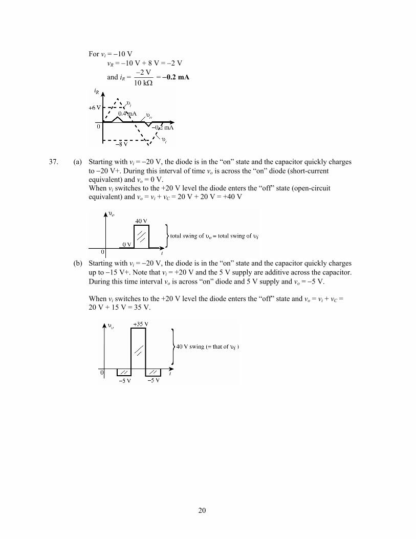
37. (a) Starting with vi = −20 V, the diode is in the “on” state and the capacitor quickly charges
to −20 V+. During this interval of time vo is across the “on” diode (short-current equivalent) and vo = 0 V.
When vi switches to the +20 V level the diode enters the “off” state (open-circuit equivalent) and vo = vi + vC = 20 V + 20 V = +40 V
(b) Starting with vi = −20 V, the diode is in the “on” state and the capacitor quickly charges
up to −15 V+. Note that vi = +20 V and the 5 V supply are additive across the capacitor. During this time interval vo is across “on” diode and 5 V supply and vo = −5 V.
When vi switches to the +20 V level the diode enters the “off” state and vo = vi + vC = 20 V + 15 V = 35 V.
21
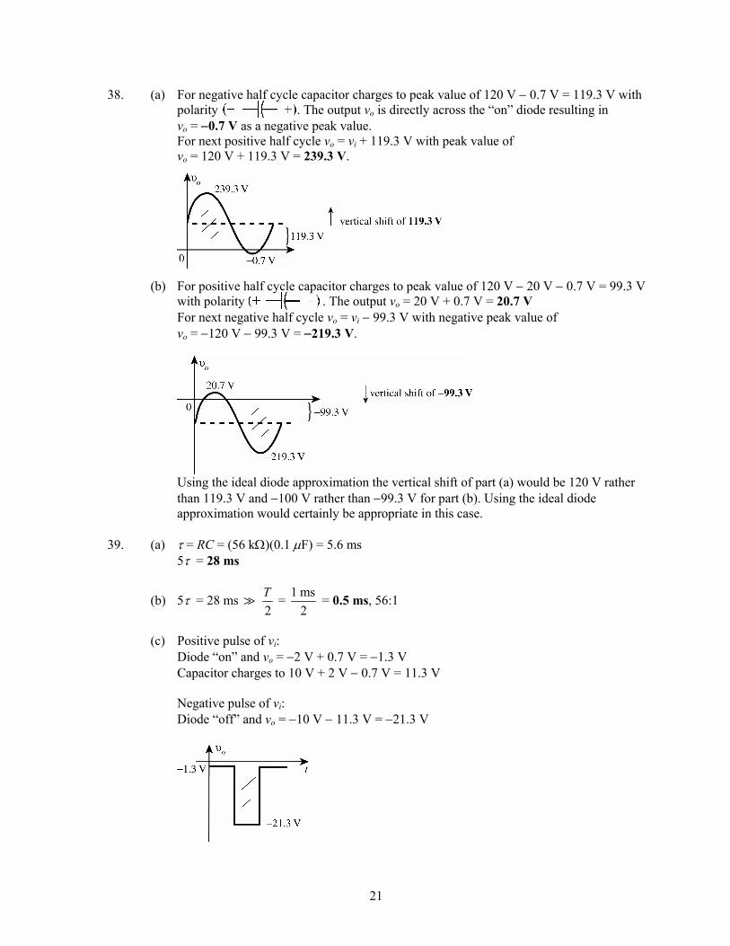
38. (a) For negative half cycle capacitor charges to peak value of 120 V − 0.7 V = 119.3 V with polarity . The output vo is directly across the “on” diode resulting in
vo = −0.7 V as a negative peak value. For next positive half cycle vo = vi + 119.3 V with peak value of vo = 120 V + 119.3 V = 239.3 V.
(b) For positive half cycle capacitor charges to peak value of 120 V − 20 V − 0.7 V = 99.3 V with polarity . The output vo = 20 V + 0.7 V = 20.7 V
For next negative half cycle vo = vi − 99.3 V with negative peak value of vo = −120 V − 99.3 V = −219.3 V.
Using the ideal diode approximation the vertical shift of part (a) would be 120 V rather
than 119.3 V and −100 V rather than −99.3 V for part (b). Using the ideal diode approximation would certainly be appropriate in this case.
39. (a) τ = RC = (56 kΩ)(0.1 μF) = 5.6 ms 5τ = 28 ms
(b) 5τ = 28 ms 2T = 1 ms
2 = 0.5 ms, 56:1
(c) Positive pulse of vi: Diode “on” and vo = −2 V + 0.7 V = −1.3 V Capacitor charges to 10 V + 2 V − 0.7 V = 11.3 V Negative pulse of vi: Diode “off” and vo = −10 V − 11.3 V = −21.3 V
22
40. Solution is network of Fig. 2.176(b) using a 10 V supply in place of the 5 V source. 41. Network of Fig. 2.178 with 2 V battery reversed.
42. (a) In the absence of the Zener diode
VL = 180 (20 V)180 220
ΩΩ+ Ω
= 9 V
VL = 9 V < VZ = 10 V and diode non-conducting
Therefore, IL = IR = 20 V220 180Ω+ Ω
= 50 mA
with IZ = 0 mA and VL = 9 V (b) In the absence of the Zener diode
VL = 470 (20 V)470 220
ΩΩ+ Ω
= 13.62 V
VL = 13.62 V > VZ = 10 V and Zener diode “on” Therefore, VL = 10 V and
sRV = 10 V / 10 V/220
s sR R sI V R= = Ω = 45.45 mA
IL = VL/RL = 10 V/470 Ω = 21.28 mA and IZ =
sRI − IL = 45.45 mA − 21.28 mA = 24.17 mA (c)
maxZP = 400 mW = VZIZ = (10 V)(IZ)
IZ = 400 mW10 V
= 40 mA
minLI =
maxsR ZI I− = 45.45 mA − 40 mA = 5.45 mA
RL = min
10 V5.45 mA
L
L
VI
= = 1,834.86 Ω
Large RL reduces IL and forces more of sRI to pass through Zener diode.
(d) In the absence of the Zener diode
VL = 10 V = (20 V)220
L
L
RR + Ω
10RL + 2200 = 20RL 10RL = 2200 RL = 220 Ω
23
43. (a) VZ = 12 V, RL = 12 V200 mA
L
L
VI
= = 60 Ω
VL = VZ = 12 V = 60 (16 V)60
L i
L s s
R VR R R
Ω=
+ Ω+
720 + 12Rs = 960 12Rs = 240 Rs = 20 Ω (b)
maxZP = VZ maxZI = (12 V)(200 mA) = 2.4 W
44. Since IL = L Z
L L
V VR R
= is fixed in magnitude the maximum value of sRI will occur when IZ is a
maximum. The maximum level of sRI will in turn determine the maximum permissible level
of Vi.
max
max
400 mW8 V
ZZ
Z
PI
V= = = 50 mA
IL = 8 V220
L Z
L L
V VR R
= =Ω
= 36.36 mA
sRI = IZ + IL = 50 mA + 36.36 mA = 86.36 mA
s
i ZR
s
V VIR−
=
or Vi = sR sI R + VZ
= (86.36 mA)(91 Ω) + 8 V = 7.86 V + 8 V = 15.86 V Any value of vi that exceeds 15.86 V will result in a current IZ that will exceed the maximum
value. 45. At 30 V we have to be sure Zener diode is “on”.
∴ VL = 20 V = 1 k (30 V)1 k
L i
L s s
R VR R R
Ω=
+ Ω +
Solving, Rs = 0.5 kΩ
At 50 V, 50 V 20 V0.5 kSRI −
=Ω
= 60 mA, IL = 20 V1 kΩ
= 20 mA
IZM = SRI − IL = 60 mA − 20 mA = 40 mA
46. For vi = +50 V: Z1 forward-biased at 0.7 V Z2 reverse-biased at the Zener potential and
2ZV = 10 V. Therefore, Vo =
1 2Z ZV V+ = 0.7 V + 10 V = 10.7 V
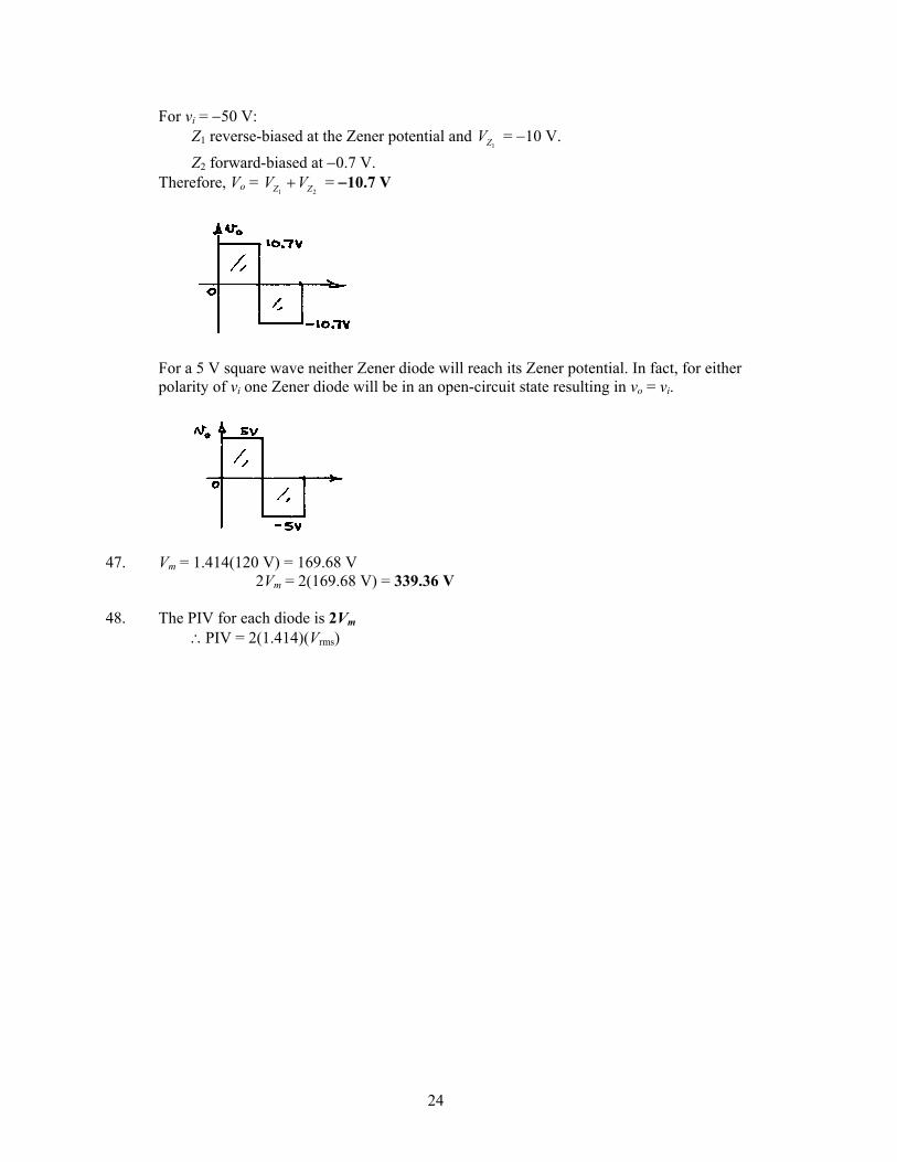
24
For vi = −50 V: Z1 reverse-biased at the Zener potential and
1ZV = −10 V. Z2 forward-biased at −0.7 V. Therefore, Vo =
1 2Z ZV V+ = −10.7 V
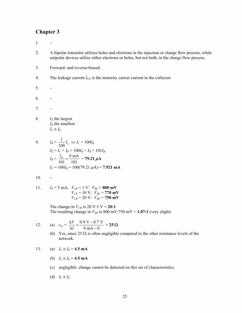
For a 5 V square wave neither Zener diode will reach its Zener potential. In fact, for either
polarity of vi one Zener diode will be in an open-circuit state resulting in vo = vi.
47. Vm = 1.414(120 V) = 169.68 V 2Vm = 2(169.68 V) = 339.36 V 48. The PIV for each diode is 2Vm ∴PIV = 2(1.414)(Vrms)
25
Chapter 3 1. − 2. A bipolar transistor utilizes holes and electrons in the injection or charge flow process, while
unipolar devices utilize either electrons or holes, but not both, in the charge flow process. 3. Forward- and reverse-biased. 4. The leakage current ICO is the minority carrier current in the collector. 5. − 6. − 7. − 8. IE the largest IB the smallest IC ≅ IE
9. IB = 1100 CI ⇒ IC = 100IB
IE = IC + IB = 100IB + IB = 101IB
IB = 8 mA101 101
EI= = 79.21 μA
IC = 100IB = 100(79.21 μA) = 7.921 mA 10. − 11. IE = 5 mA, VCB = 1 V: VBE = 800 mV VCB = 10 V: VBE = 770 mV VCB = 20 V: VBE = 750 mV The change in VCB is 20 V:1 V = 20:1 The resulting change in VBE is 800 mV:750 mV = 1.07:1 (very slight)
12. (a) rav = 0.9 V 0.7 V8 mA 0
VI
Δ −=
Δ − = 25 Ω
(b) Yes, since 25 Ω is often negligible compared to the other resistance levels of the network.
13. (a) IC ≅ IE = 4.5 mA (b) IC ≅ IE = 4.5 mA (c) negligible: change cannot be detected on this set of characteristics. (d) IC ≅ IE
26
14. (a) Using Fig. 3.7 first, IE ≅ 7 mA Then Fig. 3.8 results in IC ≅ 7 mA (b) Using Fig. 3.8 first, IE ≅ 5 mA Then Fig. 3.7 results in VBE ≅ 0.78 V (c) Using Fig. 3.10(b) IE = 5 mA results in VBE ≅ 0.81 V (d) Using Fig. 3.10(c) IE = 5 mA results in VBE = 0.7 V (e) Yes, the difference in levels of VBE can be ignored for most applications if voltages of
several volts are present in the network. 15. (a) IC = α IE = (0.998)(4 mA) = 3.992 mA (b) IE = IC + IB ⇒ IC = IE − IB = 2.8 mA − 0.02 mA = 2.78 mA
αdc = 2.78 mA2.8 mA
C
E
II
= = 0.993
(c) IC = βIB = 0.981 1 0.98BIα
α⎛ ⎞ ⎛ ⎞=⎜ ⎟ ⎜ ⎟− −⎝ ⎠ ⎝ ⎠
(40 μA) = 1.96 mA
IE = 1.96 mA0.993
CIα
= = 2 mA
16. − 17. Ii = Vi/Ri = 500 mV/20 Ω = 25 mA IL ≅ Ii = 25 mA VL = ILRL = (25 mA)(1 kΩ) = 25 V
Av = 25 V0.5 V
o
i
VV
= = 50
18. Ii = 200 mV 200 mV20 100 120
i
i s
VR R
= =+ Ω + Ω Ω
= 1.67 mA
IL = Ii = 1.67 mA VL = ILR = (1.67 mA)(5 kΩ) = 8.35 V
Av = 8.35 V0.2 V
o
i
VV
= = 41.75
19. − 20. (a) Fig. 3.14(b): IB ≅ 35μA Fig. 3.14(a): IC ≅ 3.6 mA (b) Fig. 3.14(a): VCE ≅ 2.5 V Fig. 3.14(b): VBE ≅ 0.72 V
27
21. (a) β = 2 mA17 A
C
B
II μ
= = 117.65
(b) α = 117.651 117.65 1
ββ
=+ +
= 0.992
(c) ICEO = 0.3 mA (d) ICBO = (1 − α)ICEO = (1 − 0.992)(0.3 mA) = 2.4 μA 22. (a) Fig. 3.14(a): ICEO ≅ 0.3 mA (b) Fig. 3.14(a): IC ≅ 1.35 mA
βdc = 1.35 mA10 A
C
B
II μ
= = 135
(c) α = 1351 136
ββ
=+
= 0.9926
ICBO ≅ (1 − α)ICEO = (1 − 0.9926)(0.3 mA) = 2.2 μA
23. (a) βdc = 6.7 mA80 A
C
B
II μ
= = 83.75
(b) βdc = 0.85 mA5 A
C
B
II μ
= = 170
(c) βdc = 3.4 mA30 A
C
B
II μ
= = 113.33
(d) βdc does change from pt. to pt. on the characteristics. Low IB, high VCE → higher betas High IB, low VCE → lower betas
24. (a) βac = 5 V
C
CEB
IVI
Δ=Δ
= 7.3 mA 6 mA 1.3 mA90 A 70 A 20 Aμ μ μ
−=
− = 65
(b) βac = 15 V
C
CEB
IVI
Δ=Δ
= 1.4 mA 0.3 mA 1.1 mA10 A 0 A 10 Aμ μ μ
−=
− = 110
(c) βac = 10 V
C
CEB
IVI
Δ=Δ
= 4.25 mA 2.35 mA 1.9 mA40 A 20 A 20 Aμ μ μ
−=
− = 95
(d) βac does change from point to point on the characteristics. The highest value was obtained at a higher level of VCE and lower level of IC. The separation between IB curves is the greatest in this region.
28
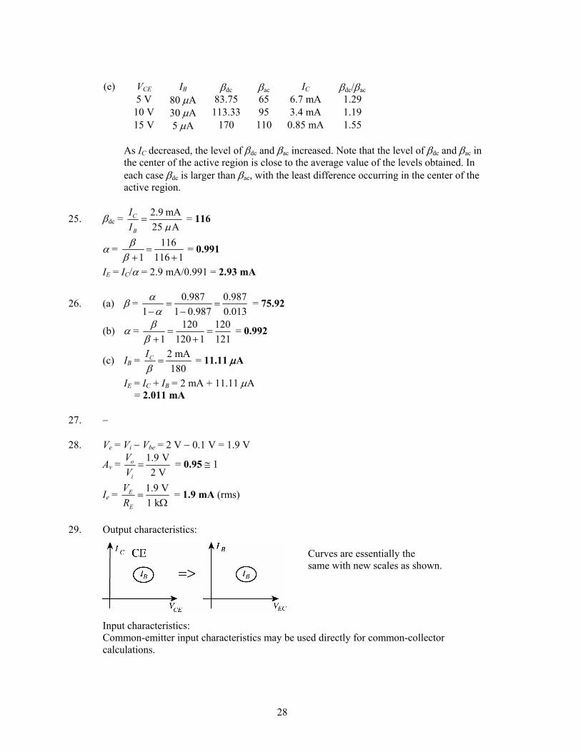
(e) VCE IB βdc βac IC βdc/βac 5 V 80 μA 83.75 65 6.7 mA 1.29 10 V 30 μA 113.33 95 3.4 mA 1.19 15 V 5 μA 170 110 0.85 mA 1.55
As IC decreased, the level of βdc and βac increased. Note that the level of βdc and βac in
the center of the active region is close to the average value of the levels obtained. In each case βdc is larger than βac, with the least difference occurring in the center of the active region.
25. βdc = 2.9 mA25 A
C
B
II μ
= = 116
α = 1161 116 1
ββ
=+ +
= 0.991
IE = IC/α = 2.9 mA/0.991 = 2.93 mA
26. (a) β = 0.987 0.9871 1 0.987 0.013αα= =
− − = 75.92
(b) α = 120 1201 120 1 121
ββ
= =+ +
= 0.992
(c) IB = 2 mA180
CIβ
= = 11.11 μA
IE = IC + IB = 2 mA + 11.11 μA = 2.011 mA 27. − 28. Ve = Vi − Vbe = 2 V − 0.1 V = 1.9 V
Av = 1.9 V2 V
o
i
VV
= = 0.95 ≅ 1
Ie = 1.9 V1 k
E
E
VR
=Ω
= 1.9 mA (rms)
29. Output characteristics: Curves are essentially the same with new scales as shown. Input characteristics: Common-emitter input characteristics may be used directly for common-collector
calculations.
29
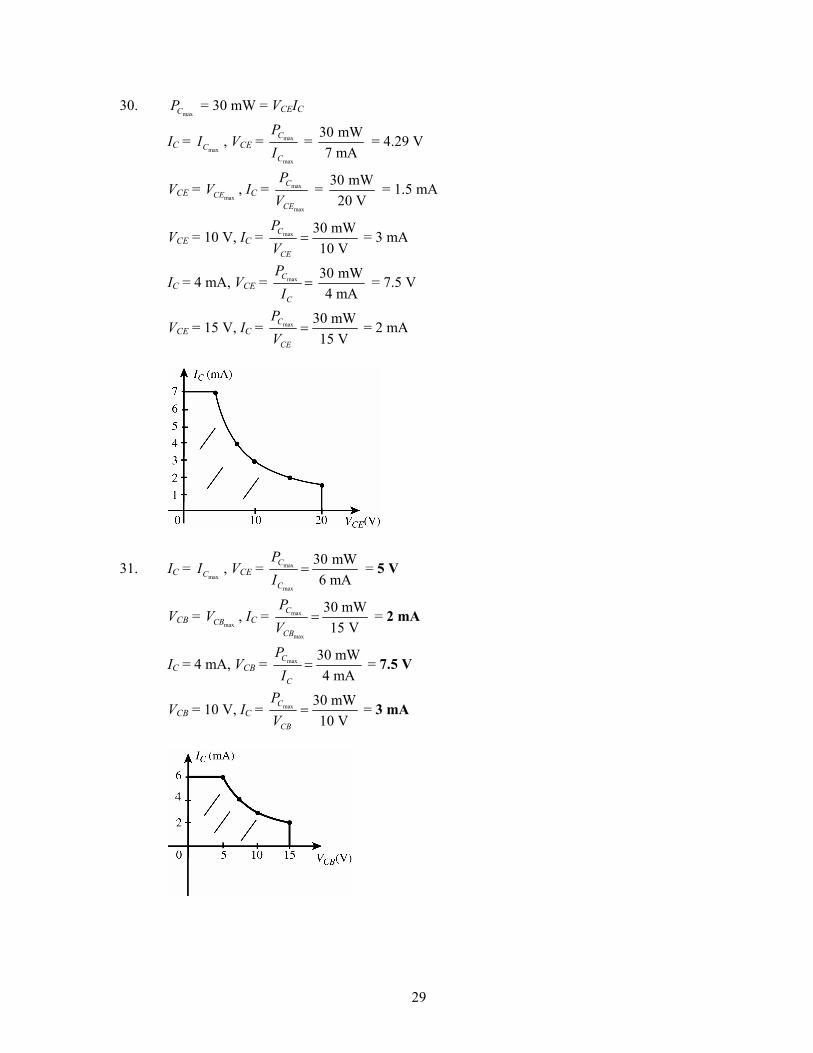
30. maxCP = 30 mW = VCEIC
IC = maxCI , VCE = max
max
C
C
PI
= 30 mW7 mA
= 4.29 V
VCE = maxCEV , IC = max
max
C
CE
PV
= 30 mW20 V
= 1.5 mA
VCE = 10 V, IC = max 30 mW10 V
C
CE
PV
= = 3 mA
IC = 4 mA, VCE = maxC
C
PI
=30 mW4 mA
= 7.5 V
VCE = 15 V, IC = max 30 mW15 V
C
CE
PV
= = 2 mA
31. IC = maxCI , VCE = max
max
30 mW6 mA
C
C
PI
= = 5 V
VCB = maxCBV , IC = max
max
30 mW15 V
C
CB
PV
= = 2 mA
IC = 4 mA, VCB = max 30 mW4 mA
C
C
PI
= = 7.5 V
VCB = 10 V, IC = max 30 mW10 V
C
CB
PV
= = 3 mA
30
32. The operating temperature range is −55°C ≤ TJ ≤ 150°C
°F = 9 C5° + 32°
= 9 ( 55 C)5− ° + 32° = −67°F
°F = 9 (150 C)5
° + 32° = 302°F
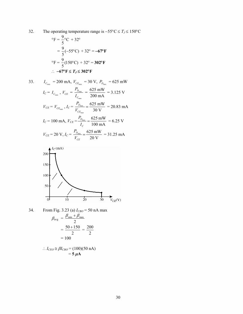
∴ −67°F ≤ TJ ≤ 302°F 33.
maxCI = 200 mA, maxCEV = 30 V,
maxDP = 625 mW
IC = maxCI , CEV = max
max
D
C
PI
= 625 mW200 mA
= 3.125 V
VCE = maxCEV , IC = max
max
625 mW30 V
D
CE
PV
= = 20.83 mA
IC = 100 mA, VCE = max 625 mW100 mA
D
C
PI
= = 6.25 V
VCE = 20 V, IC = max 625 mW20 V
D
CE
PV
= = 31.25 mA
34. From Fig. 3.23 (a) ICBO = 50 nA max
βavg = min max
2β β+
= 50 1502+ = 200
2
= 100 ∴ICEO ≅ βICBO = (100)(50 nA) = 5 μA
31
35. hFE (βdc) with VCE = 1 V, T = 25°C IC = 0.1 mA, hFE ≅ 0.43(100) = 43 ↓ IC = 10 mA, hFE ≅ 0.98(100) = 98 hfe(βac) with VCE = 10 V, T = 25°C IC = 0.1 mA, hfe ≅ 72 ↓ IC = 10 mA, hfe ≅ 160 For both hFE and hfe the same increase in collector current resulted in a similar increase
(relatively speaking) in the gain parameter. The levels are higher for hfe but note that VCE is higher also.
36. As the reverse-bias potential increases in magnitude the input capacitance Cibo decreases (Fig.
3.23(b)). Increasing reverse-bias potentials causes the width of the depletion region to
increase, thereby reducing the capacitance ACd
⎛ ⎞=∈⎜ ⎟⎝ ⎠
.
37. (a) At IC = 1 mA, hfe ≅ 120 At IC = 10 mA, hfe ≅ 160 (b) The results confirm the conclusions of problems 23 and 24 that beta tends to increase
with increasing collector current.
39. (a) βac = 3 V
C
CEB
IVI
Δ=Δ
= 16 mA 12.2 mA 3.8 mA80 A 60 A 20 Aμ μ μ
−=
− = 190
(b) βdc = 12 mA59.5 A
C
B
II μ
= = 201.7
(c) βac = 4 mA 2 mA 2 mA18 A 8 A 10 Aμ μ μ
−=
− = 200
(d) βdc = 3 mA13 A
C
B
II μ
= = 230.77
(e) In both cases βdc is slightly higher than βac (≅ 10%) (f)(g) In general βdc and βac increase with increasing IC for fixed VCE and both decrease for
decreasing levels of VCE for a fixed IE. However, if IC increases while VCE decreases when moving between two points on the characteristics, chances are the level of βdc or βac may not change significantly. In other words, the expected increase due to an increase in collector current may be offset by a decrease in VCE. The above data reveals that this is a strong possibility since the levels of β are relatively close.
32
Chapter 4
1. (a) 16 V 0.7 V 15.3 V470 k 470 kQ
CC BEB
B
V VIR− −
= = =Ω Ω
= 32.55 μA
(b) Q QC BI Iβ= = (90)(32.55 μA) = 2.93 mA
(c) Q QCE CC C CV V I R= − = 16 V − (2.93 mA)(2.7 kΩ) = 8.09 V
(d) VC = QCEV = 8.09 V
(e) VB = VBE = 0.7 V
(f) VE = 0 V 2. (a) IC = βIB = 80(40 μA) = 3.2 mA
(b) RC = 12 V 6 V 6 V3.2 mA 3.2 mA
CR CC C
C C
V V VI I
− −= = = = 1.875 kΩ
(c) RB = 12 V 0.7 V 11.3 V40 A 40 A
BR
B
VI μ μ
−= = = 282.5 kΩ
(d) VCE = VC = 6 V
3. (a) IC = IE − IB = 4 mA − 20 μA = 3.98 mA ≅ 4 mA
(b) VCC = VCE + ICRC = 7.2 V + (3.98 mA)(2.2 kΩ)
= 15.96 V ≅ 16 V
(c) β = 3.98 mA20 A
C
B
II μ
= = 199 ≅ 200
(d) RB = 15.96 V 0.7 V20 A
BR CC BE
B B
V V VI I μ
− −= = = 763 kΩ
4. satCI = 16 V
2.7 kCC
C
VR
=Ω
= 5.93 mA
5. (a) Load line intersects vertical axis at IC = 21 V3 kΩ
= 7 mA
and horizontal axis at VCE = 21 V.
(b) IB = 25 μA: RB = 21 V 0.7 V25 A
CC BE
B
V VI μ− −
= = 812 kΩ
(c) QCI ≅ 3.4 mA,
QCEV ≅ 10.75 V
33
(d) β = 3.4 mA25 A
C
B
II μ
= = 136
(e) α = 136 1361 136 1 137
ββ
= =+ +
= 0.992
(f) satCI = 21 V
3 kCC
C
VR
=Ω
= 7 mA
(g) −
(h) PD = Q QCE CV I = (10.75 V)(3.4 mA) = 36.55 mW
(i) Ps = VCC(IC + IB) = 21 V(3.4 mA + 25 μA) = 71.92 mW
(j) PR = Ps − PD = 71.92 mW − 36.55 mW = 35.37 mW
6. (a) 20 V 0.7 V( 1) 510 k (101)1.5 kQ
CC BEB
B E
V VIR Rβ
− −= =
+ + Ω + Ω = 19.3 V
661.5 kΩ
= 29.18 μA (b)
Q QC BI Iβ= = (100)(29.18 μA) = 2.92 mA (c)
QCEV = VCC − IC(RC + RE) = 20 V − (2.92 mA)(2.4 kΩ + 1.5 kΩ)
= 20 V − 11.388 V = 8.61 V (d) VC = VCC − ICRC = 20 V − (2.92 mA)(2.4 kΩ) = 20 V − 7.008 V = 13 V (e) VB = VCC − IBRB = 20 V − (29.18 μA)(510 kΩ) = 20 V − 14.882 V = 5.12 V (f) VE = VC − VCE = 13 V − 8.61 V = 4.39 V
7. (a) RC = 12 V 7.6 V 4.4 V2 mA 2 mA
CC C
C
V VI− −
= = = 2.2 kΩ
(b) IE ≅ IC: RE = 2.4 V2 mA
E
E
VI
= = 1.2 kΩ
(c) RB = 12 V 0.7 V 2.4 V 8.9 V2 mA/80 25 A
BR CC BE E
B B
V V V VI I μ
− − − −= = = = 356 kΩ
(d) VCE = VC − VE = 7.6 V − 2.4 V = 5.2 V
(e) VB = VBE + VE = 0.7 V + 2.4 V = 3.1 V
34
8. (a) IC ≅ IE = 2.1 V0.68 k
E
E
VR
=Ω
= 3.09 mA
β = 3.09 mA20 A
C
B
II μ
= = 154.5
(b) VCC = CRV + VCE + VE
= (3.09 mA)(2.7 kΩ) + 7.3 V + 2.1 V = 8.34 V + 7.3 V + 2.1 V = 17.74 V
(c) RB = 17.74 V 0.7 V 2.1 V20 A
BR CC BE E
B B
V V V VI I μ
− − − −= =
= 14.94 V20 Aμ
= 747 kΩ
9. sot
20 V 20 V2.4 k 1.5 k 3.9 k
CCC
C E
VIR R
= = =+ Ω + Ω Ω
= 5.13 mA
10. (a) satCI = 6.8 mA = 24 V
1.2 kCC
C E C
VR R R
=+ + Ω
RC + 1.2 kΩ = 24 V6.8 mA
= 3.529 kΩ
RC = 2.33 kΩ
(b) β = 4 mA30 A
C
B
II μ
= = 133.33
(c) RB = 24 V 0.7 V (4 mA)(1.2 k )30 A
BR CC BE E
B B
V V V VI I μ
− − − − Ω= =
= 18.5 V30 Aμ
= 616.67 kΩ
(d) PD =
Q QCE CV I
= (10 V)(4 mA) = 40 mW (e) P = 2
C CI R = (4 mA)2(2.33 kΩ) = 37.28 mW
11. (a) Problem 1: QCI = 2.93 mA,
QCEV = 8.09 V
(b) QBI = 32.55 μA (the same)
Q QC BI Iβ= = (135)(32.55 μA) = 4.39 mA
Q QCE CC C CV V I R= − = 16 V − (4.39 mA)(2.7 kΩ) = 4.15 V
35
(c) %ΔIC = 4.39 mA 2.93 mA2.93 mA
− × 100% = 49.83%
%ΔVCE = 4.15 V 8.09 V8.09 V
− × 100% = 48.70%
Less than 50% due to level of accuracy carried through calculations.
(d) Problem 6: QCI = 2.92 mA,
QCEV = 8.61 V (QBI = 29.18 μA)
(e) 20 V 0.7 V( 1) 510 k (150 1)(1.5 k )Q
CC BEB
B E
V VIR Rβ
− −= =
+ + Ω + + Ω = 26.21 μA
Q QC BI Iβ= = (150)(26.21 μA) = 3.93 mA
QCEV = VCC − IC(RC + RE)
= 20 V − (3.93 mA)(2.4 kΩ + 1.5 kΩ) = 4.67 V
(f) %ΔIC = 3.93 mA 2.92 mA2.92 mA
− × 100% = 34.59%
%ΔVCE = 4.67 V 8.61 V8.61 V
− × 100% = 46.76%
(g) For both IC and VCE the % change is less for the emitter-stabilized.
12. βRE ?≥ 10R2
(80)(0.68 kΩ) ≥ 10(9.1 kΩ) 54.4 kΩ ≥ 91 kΩ (No!)
(a) Use exact approach: RTh = R1 || R2 = 62 kΩ || 9.1 kΩ = 7.94 kΩ
ETh = 2
2 1
(9.1 k )(16 V)9.1 k 62 k
CCR VR R
Ω=
+ Ω + Ω = 2.05 V
2.05 V 0.7 V( 1) 7.94 k (81)(0.68 k )Q
Th BEB
Th E
E VIR Rβ
− −= =
+ + Ω + Ω
= 21.42 μA
(b) Q QC BI Iβ= = (80)(21.42 μA) = 1.71 mA
(c)
QCEV = VCC − QCI (RC + RE)
= 16 V − (1.71 mA)(3.9 kΩ + 0.68 kΩ) = 8.17 V
(d) VC = VCC − ICRC = 16 V − (1.71 mA)(3.9 kΩ) = 9.33 V
(e) VE = IERE ≅ ICRE = (1.71 mA)(0.68 kΩ) = 1.16 V
(f) VB = VE + VBE = 1.16 V + 0.7 V = 1.86 V
36
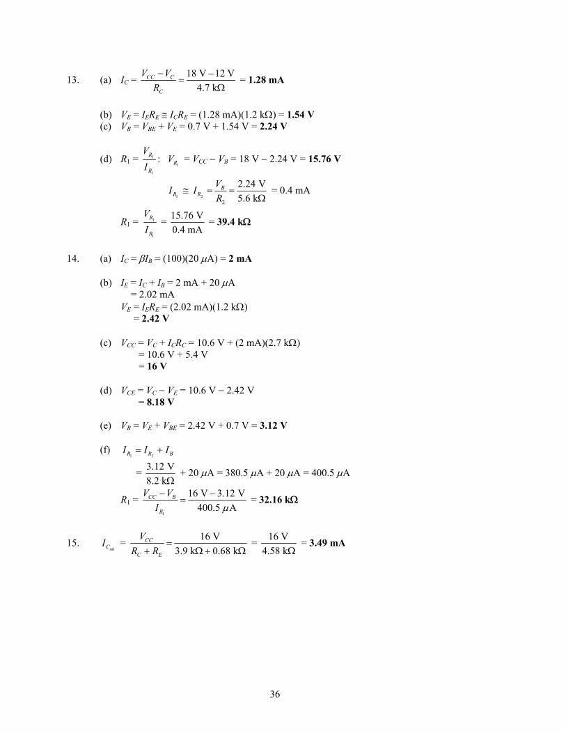
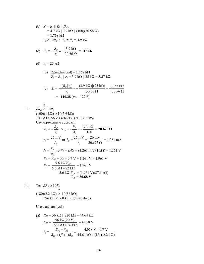
13. (a) IC = 18 V 12 V4.7 k
CC C
C
V VR− −
=Ω
= 1.28 mA
(b) VE = IERE ≅ ICRE = (1.28 mA)(1.2 kΩ) = 1.54 V (c) VB = VBE + VE = 0.7 V + 1.54 V = 2.24 V
(d) R1 = 1
1
:R
R
VI
1RV = VCC − VB = 18 V − 2.24 V = 15.76 V
1RI ≅
22
2.24 V5.6 k
BR
VIR
= =Ω
= 0.4 mA
R1 = 1
1
R
R
VI
= 15.76 V0.4 mA
= 39.4 kΩ
14. (a) IC = βIB = (100)(20 μA) = 2 mA (b) IE = IC + IB = 2 mA + 20 μA = 2.02 mA VE = IERE = (2.02 mA)(1.2 kΩ) = 2.42 V (c) VCC = VC + ICRC = 10.6 V + (2 mA)(2.7 kΩ) = 10.6 V + 5.4 V = 16 V (d) VCE = VC − VE = 10.6 V − 2.42 V = 8.18 V (e) VB = VE + VBE = 2.42 V + 0.7 V = 3.12 V (f)
1 2R R BI I I= +
= 3.12 V8.2 kΩ
+ 20 μA = 380.5 μA + 20 μA = 400.5 μA
R1 = 1
16 V 3.12 V400.5 A
CC B
R
V VI μ− −
= = 32.16 kΩ
15. satCI = 16 V
3.9 k 0.68 kCC
C E
VR R
=+ Ω + Ω
= 16 V4.58 kΩ
= 3.49 mA
37
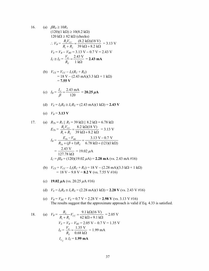
16. (a) βRE ≥ 10R2 (120)(1 kΩ) ≥ 10(8.2 kΩ) 120 kΩ ≥ 82 kΩ (checks)
∴VB = 2
1 2
(8.2 k )(18 V)39 k 8.2 k
CCR VR R
Ω=
+ Ω + Ω = 3.13 V
VE = VB − VBE = 3.13 V − 0.7 V = 2.43 V
IC ≅ IE = 2.43 V1 k
E
E
VR
=Ω
= 2.43 mA
(b) VCE = VCC − IC(RC + RE) = 18 V − (2.43 mA)(3.3 kΩ + 1 kΩ) = 7.55 V
(c) IB = 2.43 mA120
CIβ
= = 20.25 μA
(d) VE = IERE ≅ ICRE = (2.43 mA)(1 kΩ) = 2.43 V (e) VB = 3.13 V 17. (a) RTh = R1 || R2 = 39 kΩ || 8.2 kΩ = 6.78 kΩ
ETh = 1 2
8.2 k (18 V)39 k 8.2 k
C CCR VR R
Ω=
+ Ω + Ω = 3.13 V
IB = 3.13 V 0.7 V( 1) 6.78 k (121)(1 k )
Th BE
Th E
E VR Rβ
− −=
+ + Ω + Ω
= 2.43 V127.78 kΩ
= 19.02 μA
IC = βIB = (120)(19.02 μA) = 2.28 mA (vs. 2.43 mA #16) (b) VCE = VCC − IC(RC + RE) = 18 V − (2.28 mA)(3.3 kΩ + 1 kΩ) = 18 V − 9.8 V = 8.2 V (vs. 7.55 V #16) (c) 19.02 μA (vs. 20.25 μA #16) (d) VE = IERE ≅ ICRE = (2.28 mA)(1 kΩ) = 2.28 V (vs. 2.43 V #16) (e) VB = VBE + VE = 0.7 V + 2.28 V = 2.98 V (vs. 3.13 V #16) The results suggest that the approximate approach is valid if Eq. 4.33 is satisfied.
18. (a) VB = 2
1 2
9.1 k (16 V)62 k 9.1 kCC
R VR R
Ω=
+ Ω + Ω = 2.05 V
VE = VB − VBE = 2.05 V − 0.7 V = 1.35 V
IE = 1.35 V0.68 k
E
E
VR
=Ω
= 1.99 mA
QCI ≅ IE = 1.99 mA
38
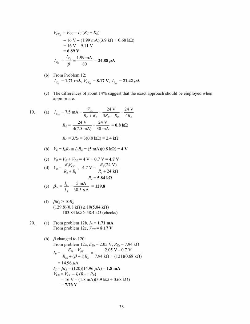
QCEV = VCC − IC (RC + RE)
= 16 V − (1.99 mA)(3.9 kΩ + 0.68 kΩ) = 16 V − 9.11 V = 6.89 V
QBI = 1.99 mA
80QCI
β= = 24.88 μA
(b) From Problem 12:
QCI = 1.71 mA, QCEV = 8.17 V,
QBI = 21.42 μA
(c) The differences of about 14% suggest that the exact approach should be employed when
appropriate.
19. (a) sat
24 V 24 V7.5 mA3 4
CCC
C E E E E
VIR R R R R
= = = =+ +
RE = 24 V 24 V4(7.5 mA) 30 mA
= = 0.8 kΩ
RC = 3RE = 3(0.8 kΩ) = 2.4 kΩ (b) VE = IERE ≅ ICRE = (5 mA)(0.8 kΩ) = 4 V (c) VB = VE + VBE = 4 V + 0.7 V = 4.7 V
(d) VB = 2
2 1
CCR VR R+
, 4.7 V = 2
2
(24 V)24 k
RR + Ω
R2 = 5.84 kΩ
(e) βdc = 5 mA38.5 A
C
B
II μ
= = 129.8
(f) βRE ≥ 10R2 (129.8)(0.8 kΩ) ≥ 10(5.84 kΩ) 103.84 kΩ ≥ 58.4 kΩ (checks) 20. (a) From problem 12b, IC = 1.71 mA From problem 12c, VCE = 8.17 V (b) β changed to 120: From problem 12a, ETh = 2.05 V, RTh = 7.94 kΩ
IB = 2.05 V 0.7 V( 1) 7.94 k + (121)(0.68 k )
Th BE
Th E
E VR Rβ
− −=
+ + Ω Ω
= 14.96 μA IC = βIB = (120)(14.96 μA) = 1.8 mA VCE = VCC − IC(RC + RE) = 16 V − (1.8 mA)(3.9 kΩ + 0.68 kΩ) = 7.76 V
39
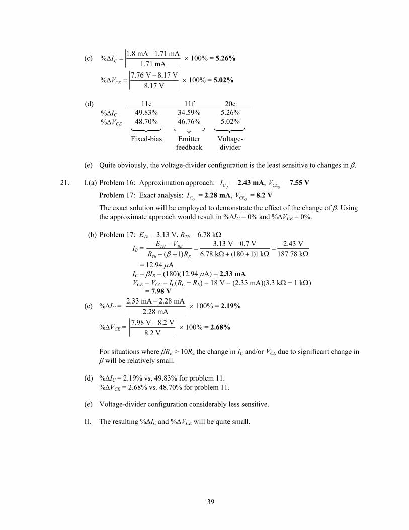
(c) 1.8 mA 1.71 mA%1.71 mACI −
Δ = × 100% = 5.26%
7.76 V 8.17 V%8.17 VCEV −
Δ = × 100% = 5.02%
(d) 11c 11f 20c %ΔIC 49.83% 34.59% 5.26% %ΔVCE 48.70% 46.76% 5.02% Fixed-bias Emitter
feedback Voltage- divider
(e) Quite obviously, the voltage-divider configuration is the least sensitive to changes in β. 21. I.(a) Problem 16: Approximation approach:
QCI = 2.43 mA, QCEV = 7.55 V
Problem 17: Exact analysis: QCI = 2.28 mA,
QCEV = 8.2 V
The exact solution will be employed to demonstrate the effect of the change of β. Using the approximate approach would result in %ΔIC = 0% and %ΔVCE = 0%.
(b) Problem 17: ETh = 3.13 V, RTh = 6.78 kΩ
IB = 3.13 V 0.7 V 2.43 V( 1) 6.78 k (180 1)1 k 187.78 k
TH BE
Th E
E VR Rβ
− −= =
+ + Ω + + Ω Ω
= 12.94 μA IC = βIB = (180)(12.94 μA) = 2.33 mA VCE = VCC − IC(RC + RE) = 18 V − (2.33 mA)(3.3 kΩ + 1 kΩ) = 7.98 V
(c) %ΔIC = 2.33 mA 2.28 mA2.28 mA
− × 100% = 2.19%
%ΔVCE = 7.98 V 8.2 V8.2 V
− × 100% = 2.68%
For situations where βRE > 10R2 the change in IC and/or VCE due to significant change in
β will be relatively small. (d) %ΔIC = 2.19% vs. 49.83% for problem 11. %ΔVCE = 2.68% vs. 48.70% for problem 11. (e) Voltage-divider configuration considerably less sensitive. II. The resulting %ΔIC and %ΔVCE will be quite small.
40
22. (a) IB = 16 V 0.7 V( ) 470 k + (120)(3.6 k 0.51 k )
CC BE
B C E
V VR R Rβ
− −=
+ + Ω Ω + Ω
= 15.88 μA (b) IC = βIB = (120)(15.88 μA) = 1.91 mA (c) VC = VCC − ICRC = 16 V − (1.91 mA)(3.6 kΩ) = 9.12 V
23. (a) IB = 30 V 0.7 V( ) 6.90 k 100(6.2 k 1.5 k )
CC BE
B C E
V VR R Rβ
− −=
+ + Ω + Ω + Ω = 20.07 μA
IC = βIB = (100)(20.07 μA) = 2.01 mA
(b) VC = VCC − ICRC = 30 V − (2.01 mA)(6.2 kΩ) = 30 V − 12.462 V = 17.54 V (c) VE = IERE ≅ ICRE = (2.01 mA)(1.5 kΩ) = 3.02 V (d) VCE = VCC − IC(RC + RE) = 30 V − (2.01 mA)(6.2 kΩ + 1.5 kΩ) = 14.52 V
24. (a) IB = 22 V 0.7 V( ) 470 k (90)(9.1 k 9.1 k )
CC BE
B C E
V VR R Rβ
− −=
+ + Ω + Ω + Ω
= 10.09 μA IC = βIB = (90)(10.09 μA) = 0.91 mA VCE = VCC − IC(RC + RE) = 22 V − (0.91 mA)(9.1 kΩ + 9.1 kΩ) = 5.44 V
(b) β = 135, IB = 22 V 0.7 V( ) 470 k (135)(9.1 k 9.1 k )
CC BE
B C E
V VR R Rβ
− −=
+ + Ω + Ω + Ω
= 7.28 μA IC = βIB = (135)(7.28 μA) = 0.983 mA VCE = VCC − IC(RC + RE) = 22 V − (0.983 mA)(9.1 kΩ + 9.1 kΩ) = 4.11 V
(c) 0.983 mA 0.91 mA%0.91 mACI −
Δ = × 100% = 8.02%
4.11 V 5.44 V%5.44 VCEV −
Δ = × 100% = 24.45%
(d) The results for the collector feedback configuration are closer to the voltage-divider
configuration than to the other two. However, the voltage-divider configuration continues to have the least sensitivities to change in β.
41
25. 1 MΩ = 0 Ω, RB = 150 kΩ
IB = 12 V 0.7 V( ) 150 k (180)(4.7 k 3.3 k )
CC BE
B C E
V VR R Rβ
− −=
+ + Ω + Ω + Ω
= 7.11 μA IC = βIB = (180)(7.11 μA) = 1.28 mA VC = VCC −ICRC = 12 V − (1.28 mA)(4.7 kΩ) = 5.98 V Full 1 MΩ: RB = 1,000 kΩ + 150 kΩ = 1,150 kΩ = 1.15 MΩ
IB = 12 V 0.7 V( ) 1.15 M (180)(4.7 k 3.3 k )
CC BE
B C E
V VR R Rβ
− −=
+ + Ω + Ω + Ω
= 4.36 μA IC = βIB = (180)(4.36 μA) = 0.785 mA VC = VCC − ICRC = 12 V − (0.785 mA)(4.7 kΩ) = 8.31 V VC ranges from 5.98 V to 8.31 V 26. (a) VE = VB − VBE = 4 V − 0.7 V = 3.3 V
(b) IC ≅ IE = 3.3 V1.2 k
E
E
VR
=Ω
= 2.75 mA
(c) VC = VCC − ICRC = 18 V − (2.75 mA)(2.2 kΩ) = 11.95 V (d) VCE = VC − VE = 11.95 V − 3.3 V = 8.65 V
(e) IB = 11.95 V 4 V330 k
BR C B
B B
V V VR R
− −= =
Ω = 24.09 μA
(f) β = 2.75 mA24.09 A
C
B
II μ
= = 114.16
27. (a) IB = 6 V + 6 V 0.7 V( 1) 330 k (121)(1.2 k )
CC EE BE
B E
V V VR Rβ
+ − −=
+ + Ω + Ω
= 23.78 μA IE = (β + 1)IB = (121)(23.78 μA) = 2.88 mA −VEE + IERE − VE = 0 VE = −VEE + IERE = −6 V + (2.88 mA)(1.2 kΩ) = −2.54 V
28. (a) IB = 12 V 0.7 V( 1) 9.1 k (120 1)15 k
EE BE
B E
V VR Rβ
− −=
+ + Ω + + Ω
= 6.2 μA (b) IC = βIB = (120)(6.2 μA) = 0.744 mA (c) VCE = VCC + VEE − IC(RC + RE) = 16 V + 12 V − (0.744 mA)(27 kΩ) = 7.91 V (d) VC = VCC − ICRC = 16 V − (0.744 mA)(12 kΩ) = 7.07 V
42
29. (a) IE = 8 V 0.7 V 7.3 V2.2 k 2.2 k−
=Ω Ω
= 3.32 mA
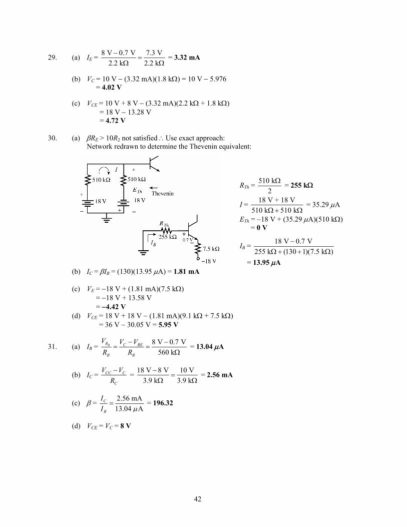
(b) VC = 10 V − (3.32 mA)(1.8 kΩ) = 10 V − 5.976 = 4.02 V (c) VCE = 10 V + 8 V − (3.32 mA)(2.2 kΩ + 1.8 kΩ) = 18 V − 13.28 V = 4.72 V 30. (a) βRE > 10R2 not satisfied ∴Use exact approach: Network redrawn to determine the Thevenin equivalent:
RTh = 510 k2Ω = 255 kΩ
I = 18 V + 18 V510 k 510 kΩ+ Ω
= 35.29 μA
ETh = −18 V + (35.29 μA)(510 kΩ) = 0 V
IB = 18 V 0.7 V255 k (130 1)(7.5 k )
−Ω + + Ω
= 13.95 μA (b) IC = βIB = (130)(13.95 μA) = 1.81 mA (c) VE = −18 V + (1.81 mA)(7.5 kΩ) = −18 V + 13.58 V = −4.42 V (d) VCE = 18 V + 18 V − (1.81 mA)(9.1 kΩ + 7.5 kΩ) = 36 V − 30.05 V = 5.95 V
31. (a) IB = 8 V 0.7 V560 k
BR C BE
B B
V V VR R
− −= =
Ω = 13.04 μA
(b) IC = CC C
C
V VR− = 18 V 8 V 10 V
3.9 k 3.9 k−
=Ω Ω
= 2.56 mA
(c) β = 2.56 mA13.04 A
C
B
II μ
= = 196.32
(d) VCE = VC = 8 V
43
32. IB = 2.5 mA80
CIβ
= = 31.25 μA
RB = 12 V 0.7 V31.25 A
BR CC BE
B B
V V VI I μ
− −= = = 361.6 kΩ
RC = 12 V 6 V 6 V2.5 mA 2.5 mA
QC
Q
CC CER CC C
C C C
V VV V VI I I
−− −= = = =
= 2.4 kΩ Standard values: RB = 360 kΩ RC = 2.4 kΩ
33. satCI = CC
C E
VR R+
= 10 mA
20 V4 E ER R+
= 10 mA ⇒ 20 V5 ER
= 10 mA ⇒ 5RE = 20 V10 mA
= 2 kΩ
RE = 2 k5Ω = 400 Ω
RC = 4RE = 1.6 kΩ
IB = 5 mA120
CIβ
= = 41.67 μA
RB = VRB/IB = 20 V 0.7 V 5 mA(0.4 k ) 19.3 2 V41.67 A 41.67 Aμ μ
− − Ω −=
= 415.17 kΩ Standard values: RE = 390 Ω, RC = 1.6 kΩ, RB = 430 kΩ
34. RE = 3 V4 mA
E E
E C
V VI I
≅ = = 0.75 kΩ
RC = ( )
QC CC CE ER CC C
C C C
V V VV V VI I I
− +−= =
= 24 V (8 V + 3 V) 24 V 11 V 13 V4 mA 4 mA 4 mA− −
= = = 3.25 kΩ
VB = VE + VBE = 3 V + 0.7 V = 3.7 V
VB = 2 2
2 1 2 1
(24 V)3.7 V = CCR V RR R R R
⎫⇒ ⎬
+ + ⎭ 2 unknowns!
∴ use βRE ≥ 10R2 for increased stability (110)(0.75 kΩ) = 10R2 R2 = 8.25 kΩ Choose R2 = 7.5 kΩ
44
Substituting in the above equation:
3.7 V = 1
7.5 k (24 V)7.5 k R
ΩΩ+
R1 = 41.15 kΩ Standard values: RE = 0.75 kΩ, RC = 3.3 kΩ, R2 = 7.5 kΩ, R1 = 43 kΩ
35. VE = 15 CCV = 1 (28 V)
5 = 5.6 V
RE = 5.6 V5 mA
E
E
VI
= = 1.12 kΩ (use 1.1 kΩ)
VC = 28 V2 2CC
EV V+ = + 5.6 V = 14 V + 5.6 V = 19.6 V
CRV = VCC − VC = 28 V − 19.6 V = 8.4 V
RC = 8.4 V5 mA
CR
C
VI
= = 1.68 kΩ (use 1.6 kΩ)
VB = VBE + VE = 0.7 V + 5.6 V = 6.3 V
VB = 2
2 1
CCR VR R+
⇒ 6.3 V = 2
2 1
(28 V)RR R+
(2 unknowns)
β = 5 mA37 A
C
B
II μ
= = 135.14
βRE = 10R2 (135.14)(1.12 kΩ) = 10(R2) R2 = 15.14 kΩ (use 15 kΩ)
Substituting: 6.3 V = 1
(15.14 k )(28 V)15.14 k R
ΩΩ+
Solving, R1 = 52.15 kΩ (use 51 kΩ) Standard values: RE = 1.1 kΩ RC = 1.6 kΩ R1 = 51 kΩ R2 = 15 kΩ
36. I2 kΩ = 18 V 0.7 V2 k−Ω
= 8.65 mA ≅ I
37. For current mirror: I(3 kΩ) = I(2.4 kΩ) = I = 2 mA 38.
QD DSSI I= = 6 mA
45
39. VB ≅ 4.3 k ( 18 V)4.3 k 4.3 k
Ω−
Ω + Ω = −9 V
VE = −9 V − 0.7 V = −9.7 V
IE = 18 V ( 9.7 V)1.8 k
− − −Ω
= 4.6 mA = I
40. IE = 5.1 V 0.7 V1.2 k
Z BE
E
V VR− −
=Ω
= 3.67 mA
41. sat
10 V2.4 k
CCC
C
VIR
= =Ω
= 4.167 mA
From characteristics maxBI ≅ 31 μA
IB = 10 V 0.7 V180 k
i BE
B
V VR− −
=Ω
= 51.67 μA
51.67 μA 31 μA, well saturated Vo = 10 V − (0.1 mA)(2.4 kΩ) = 10 V − 0.24 V = 9.76 V
42. satCI = 8 mA = 5 V
CR
RC = 5 V8 mA
= 0.625 kΩ
maxBI = sat 8 mA
100CIβ
= = 80 μA
Use 1.2 (80 μA) = 96 μA
RB = 5 V 0.7 V96 Aμ− = 44.79 kΩ
Standard values: RB = 43 kΩ RC = 0.62 kΩ
46
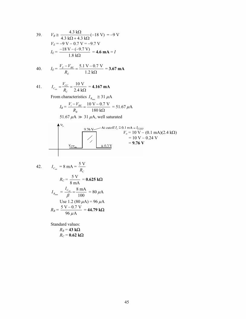
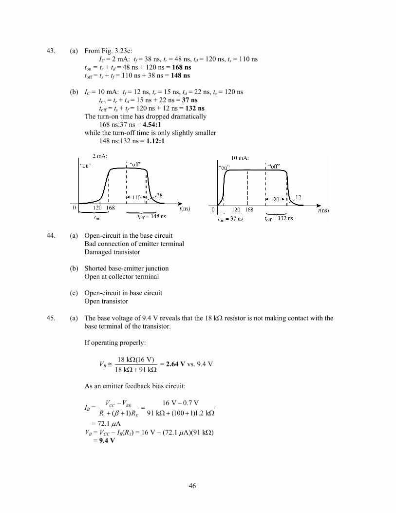
43. (a) From Fig. 3.23c: IC = 2 mA: tf = 38 ns, tr = 48 ns, td = 120 ns, ts = 110 ns ton = tr + td = 48 ns + 120 ns = 168 ns toff = ts + tf = 110 ns + 38 ns = 148 ns (b) IC = 10 mA: tf = 12 ns, tr = 15 ns, td = 22 ns, ts = 120 ns ton = tr + td = 15 ns + 22 ns = 37 ns toff = ts + tf = 120 ns + 12 ns = 132 ns The turn-on time has dropped dramatically 168 ns:37 ns = 4.54:1 while the turn-off time is only slightly smaller 148 ns:132 ns = 1.12:1
44. (a) Open-circuit in the base circuit Bad connection of emitter terminal Damaged transistor (b) Shorted base-emitter junction Open at collector terminal (c) Open-circuit in base circuit Open transistor 45. (a) The base voltage of 9.4 V reveals that the 18 kΩ resistor is not making contact with the
base terminal of the transistor. If operating properly:
VB ≅ 18 k (16 V)18 k 91 k
ΩΩ+ Ω
= 2.64 V vs. 9.4 V
As an emitter feedback bias circuit:
IB = 1
16 V 0.7 V( 1) 91 k (100 1)1.2 k
CC BE
E
V VR Rβ
− −=
+ + Ω + + Ω
= 72.1 μA VB = VCC − IB(R1) = 16 V − (72.1 μA)(91 kΩ) = 9.4 V
47
(b) Since VE > VB the transistor should be “off”
With IB = 0 μA, VB = 18 k (16 V)18 k 91 k
ΩΩ+ Ω
= 2.64 V
∴ Assume base circuit “open” The 4 V at the emitter is the voltage that would exist if the transistor were shorted
collector to emitter.
VE = 1.2 k (16 V)1.2 k 3.6 k
ΩΩ+ Ω
= 4 V
46. (a) RB↑, IB↓, IC↓, VC↑ (b) β↓, IC↓ (c) Unchanged,
satCI not a function of β (d) VCC↓, IB↓, IC↓ (e) β↓, IC↓,
CRV ↓ , ERV ↓ , VCE↑
47. (a) IB = ( 1)
Th BE Th BE
Th E Th E
E V E VR R R Rβ β
− −≅
+ + +
IC = βIB = Th BE Th BE
ThTh EE
E V E VRR R R
ββ
β
⎡ ⎤− −=⎢ ⎥+⎣ ⎦ +
As β↑, ThRβ
↓, IC↑, CRV ↑
VC = VCC − CRV
and VC↓ (b) R2 = open, IB↑, IC↑ VCE = VCC − IC(RC + RE) and VCE↓ (c) VCC↓, VB↓, VE↓, IE↓, IC↓ (d) IB = 0 μA, IC = ICEO and IC(RC + RE) negligible with VCE ≅ VCC = 20 V (e) Base-emitter junction = short IB↑ but transistor action lost and IC = 0 mA with VCE = VCC = 20 V 48. (a) RB open, IB = 0 μA, IC = ICEO ≅ 0 mA and VC ≅ VCC = 18 V (b) β↑, IC↑,
CRV , ERV , VCE↓
(c) RC↓, IB↑, IC↑, VE↑ (d) Drop to a relatively low voltage ≅ 0.06 V (e) Open in the base circuit
↑ ↑
48
49. IB = 12 V 0.7 V 11.3 V510 k 510 k
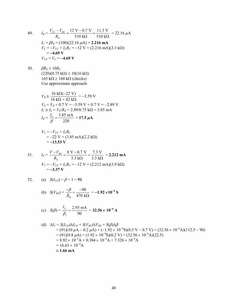
CC BE
B
V VR− −
= =Ω Ω
= 22.16 μA
IC = βIB = (100)(22.16 μA) = 2.216 mA VC = −VCC + ICRC = −12 V + (2.216 mA)(3.3 kΩ) = −4.69 V VCE = VC = −4.69 V 50. βRE ≥ 10R2 (220)(0.75 kΩ) ≥ 10(16 kΩ) 165 kΩ ≥ 160 kΩ (checks) Use approximate approach:
VB ≅ 16 k ( 22 V)16 k + 82 k
Ω −Ω Ω
= −3.59 V
VE = VB + 0.7 V = −3.59 V + 0.7 V = −2.89 V IC ≅ IE = VE/RE = 2.89/0.75 kΩ = 3.85 mA
IB = 3.85 mA220
CIβ
= = 17.5 μA
VC = −VCC + ICRC = −22 V + (3.85 mA)(2.2 kΩ) = −13.53 V
51. IE = 8 V 0.7 V 7.3 V3.3 k 3.3 k
BE
E
V VR− −
= =Ω Ω
= 2.212 mA
VC = −VCC + ICRC = −12 V + (2.212 mA)(3.9 kΩ) = −3.37 V 52. (a) S(ICO) = β + 1 = 91
(b) S(VBE) = 90470 kBR
β− −=
Ω = −1.92 ×10⁻⁴ S
(c) S(β) = 1
1
2.93 mA90
CIβ
= = 32.56 × 10⁻⁶ A
(d) ΔIC = S(ICO)ΔICO + S(VBE)ΔVBE + S(β)Δβ = (91)(10 μA − 0.2 μA) + (−1.92 × 10⁻⁴S)(0.5 V − 0.7 V) + (32.56 × 10⁻⁶A)(112.5 − 90) = (91)(9.8 μA) + (1.92 × 10⁻⁴S)(0.2 V) + (32.56 × 10⁻⁶A)(22.5) = 8.92 × 10⁻⁴A + 0.384 × 10⁻⁴A + 7.326 × 10⁻⁴A = 16.63 × 10⁻⁴A ≅ 1.66 mA
49
53. For the emitter-bias:
(a) S(ICO) = (β + 1) (1 / ) (1 510 k /1.5 k )(100 1)( 1) / (100 1) 510 k /1.5 k
B E
B E
R RR Rβ
+ + Ω Ω= +
+ + + + Ω Ω
= 78.1
(b) S(VBE) = 100( 1) 510 k (100 1)1.5 kB ER Rββ− −
=+ + Ω + + Ω
= −1.512 × 10⁻⁴S
(c) S(β) = 1
1 2
(1 / ) 2.92 mA(1 + 340)(1 / ) 100(1 125 340)
C B E
B E
I R RR Rβ β
+=
+ + + +
= 21.37 × 10⁻⁶A (d) ΔIC = S(ICO)ΔICO + S(VBE)ΔVBE + S(β)Δβ = (78.1)(9.8 μA) + (−1.512 × 10⁻¹⁴S)(−0.2 V) + (21.37 × 10⁻⁶ A)(25) = 0.7654 mA + 0.0302 mA + 0.5343 mA = 1.33 mA 54. (a) RTh = 62 kΩ || 9.1 kΩ = 7.94 kΩ
S(ICO) = (β + 1) 1 / (1 7.94 k / 0.68 k )(80 1)( 1) / (80 1) 7.94 k / 0.68 k
Th E
Th E
R RR Rβ
+ + Ω Ω= +
+ + + + Ω Ω
= (81)(1 11.68)81 11.68
++
= 11.08
(b) S(VBE) = 80( 1) 7.94 k (81)(0.68 k )Th ER Rββ− −
=+ + Ω + Ω
= 807.94 k 55.08 k
−Ω + Ω
= −1.27 × 10⁻³S
(c) S(β) = 1
1 2
(1 / ) 1.71 mA(1 + 7.94 k / 0.68 k )(1 / ) 80(1 100 7.94 k / 0.68 k )
C Th E
Th E
I R RR Rβ β
+ Ω Ω=
+ + + + Ω Ω
= 1.71 mA(12.68)80(112.68)
= 2.41 × 10⁻⁶ A
(d) ΔIC = S(ICO)ΔICO + S(VBE) ΔVBE + S(β)Δβ = (11.08)(10 μA − 0.2 μA) + (−1.27 × 10⁻³S)(0.5 V − 0.7 V) + (2.41 × 10⁻⁶A)(100 − 80) = (11.08)(9.8 μA) + (−1.27 × 10⁻³S)(−0.2 V) + (2.41 × 10⁻⁶A)(20) = 1.09 × 10⁻⁴A + 2.54 × 10⁻⁴A + 0.482 × 10⁻⁴A = 4.11 × 10⁻⁴A = 0.411 mA
50
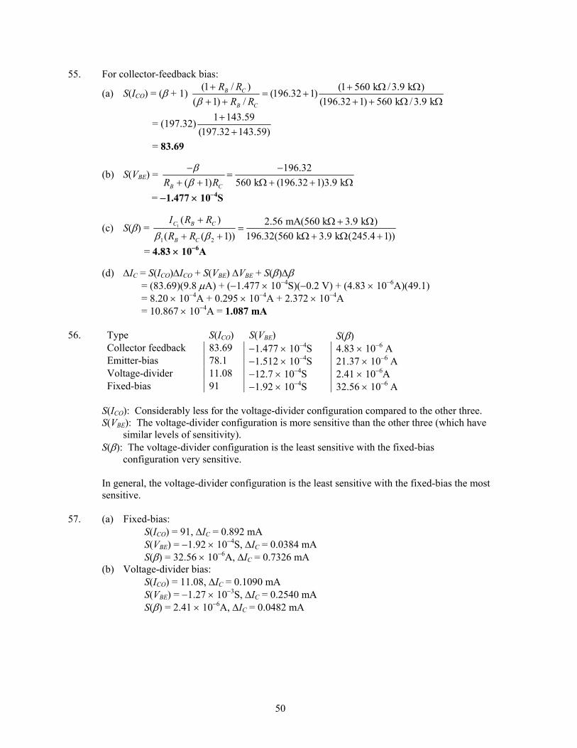
55. For collector-feedback bias:
(a) S(ICO) = (β + 1) (1 / ) (1 560 k / 3.9 k )(196.32 1)( 1) / (196.32 1) 560 k / 3.9 k
B C
B C
R RR Rβ
+ + Ω Ω= +
+ + + + Ω Ω
= (197.32) 1 143.59(197.32 143.59)
++
= 83.69
(b) S(VBE) = 196.32( 1) 560 k (196.32 1)3.9 kB CR Rββ− −
=+ + Ω + + Ω
= −1.477 × 10⁻⁴S
(c) S(β) = 1
1 2
( ) 2.56 mA(560 k 3.9 k )( ( 1)) 196.32(560 k 3.9 k (245.4 1))
C B C
B C
I R RR Rβ β
+ Ω + Ω=
+ + Ω + Ω +
= 4.83 × 10⁻⁶A (d) ΔIC = S(ICO)ΔICO + S(VBE) ΔVBE + S(β)Δβ = (83.69)(9.8 μA) + (−1.477 × 10⁻⁴S)(−0.2 V) + (4.83 × 10⁻⁶A)(49.1) = 8.20 × 10⁻⁴A + 0.295 × 10⁻⁴A + 2.372 × 10⁻⁴A = 10.867 × 10⁻⁴A = 1.087 mA 56. Type S(ICO) S(VBE) S(β) Collector feedback 83.69 −1.477 × 10⁻⁴S 4.83 × 10⁻⁶ A Emitter-bias 78.1 −1.512 × 10⁻⁴S 21.37 × 10⁻⁶ A Voltage-divider 11.08 −12.7 × 10⁻⁴S 2.41 × 10⁻⁶A Fixed-bias 91 −1.92 × 10⁻⁴S 32.56 × 10⁻⁶ A S(ICO): Considerably less for the voltage-divider configuration compared to the other three. S(VBE): The voltage-divider configuration is more sensitive than the other three (which have
similar levels of sensitivity). S(β): The voltage-divider configuration is the least sensitive with the fixed-bias
configuration very sensitive.
In general, the voltage-divider configuration is the least sensitive with the fixed-bias the most sensitive.
57. (a) Fixed-bias: S(ICO) = 91, ΔIC = 0.892 mA S(VBE) = −1.92 × 10⁻⁴S, ΔIC = 0.0384 mA S(β) = 32.56 × 10⁻⁶A, ΔIC = 0.7326 mA (b) Voltage-divider bias: S(ICO) = 11.08, ΔIC = 0.1090 mA S(VBE) = −1.27 × 10⁻³S, ΔIC = 0.2540 mA S(β) = 2.41 × 10⁻⁶A, ΔIC = 0.0482 mA
51
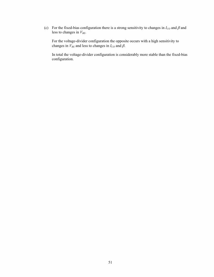
(c) For the fixed-bias configuration there is a strong sensitivity to changes in ICO and β and less to changes in VBE.
For the voltage-divider configuration the opposite occurs with a high sensitivity to
changes in VBE and less to changes in ICO and β. In total the voltage-divider configuration is considerably more stable than the fixed-bias
configuration.
52
Chapter 5 1. (a) If the dc power supply is set to zero volts, the amplification will be zero. (b) Too low a dc level will result in a clipped output waveform. (c) Po = I2R = (5 mA)22.2 kΩ = 55 mW Pi = VCCI = (18 V)(3.8 mA) = 68.4 mW
(ac) 55 mW(dc) 68.4 mW
o
i
PP
η = = = 0.804 ⇒ 80.4%
2. −
3. xC = 1 12 2 (1 kHz)(10 F)fCπ π μ
= = 15.92 Ω
f = 100 kHz: xC = 0.159 Ω Yes, better at 100 kHz 4. −
5. (a) Zi = 10 mV0.5 mA
i
i
VI=
= 20 Ω (=re) (b) Vo = IcRL = αIcRL = (0.98)(0.5 mA)(1.2 kΩ) = 0.588 V
(c) Av = 0.588 V10 mV
o
i
VV
=
= 58.8 (d) Zo = ∞ Ω
(e) Ai = o
i
II
= e
e
IIα = α = 0.98
(f) Ib = Ie − Ic = 0.5 mA − 0.49 mA = 10 μA
53
6. (a) re = 48 mV3.2 mA
i
i
VI= = 15 Ω
(b) Zi = re = 15 Ω (c) IC = αIe = (0.99)(3.2 mA) = 3.168 mA (d) Vo = ICRL = (3.168 mA)(2.2 kΩ) = 6.97 V
(e) Av = 6.97 V48 mV
o
i
VV
= = 145.21
(f) Ib = (1 − α)Ie = (1 − 0.99)Ie = (0.01)(3.2 mA) = 32 μA
7. (a) re = 26 mV 26 mV(dc) 2 mAEI
= = 13 Ω
Zi = βre = (80)(13 Ω) = 1.04 kΩ
(b) Ib = 1 1
C e e eI I I Iβαβ β β β β
= = ⋅ =+ +
= 2 mA81
= 24.69 μA
(c) Ai = o L
i b
I II I=
IL = ( )o b
o L
r Ir Rβ+
Ai =
ob
o L o
b o L
r Ir R r
I r R
ββ
⋅+
= ⋅+
= 40 k (80)40 k 1.2 k
ΩΩ+ Ω
= 77.67
(d) Av = 1.2 k 40 k
13L o
e
R rr
Ω Ω− = −
Ω
= 1.165 k13
Ω−
Ω
= −89.6
54
8. (a) Zi = βre = (140)re = 1200
re = 1200140
= 8.571 Ω
(b) Ib = 30 mV1.2 k
i
i
VZ
=Ω
= 25 μA
(c) Ic = βIb = (140)(25 μA) = 3.5 mA
(d) IL = (50 k )(3.5 mA)50 k 2.7 k
o c
o L
r Ir R
Ω=
+ Ω + Ω = 3.321 mA
Ai = 3.321 mA25 A
L
i
II μ= = 132.84
(e) Av = o i L
i i
V A RV Z
−= = (2.7 k )(132.84)
1.2 kΩ
−Ω
= −298.89
9. (a) re: IB = 12 V 0.7 V220 k
CC BE
B
V VR− −
=Ω
= 51.36 μA
IE = (β + 1)IB = (60 + 1)(51.36 μA) = 3.13 mA
re = 26 mV 26 mV3.13 mAEI
= = 8.31 Ω
Zi = RB || βre = 220 kΩ || (60)(8.31 Ω) = 220 kΩ || 498.6 Ω = 497.47 Ω ro ≥ 10RC ∴ Zo = RC = 2.2 kΩ
(b) Av = 2.2 k8.31
C
e
Rr
− Ω− =
Ω = −264.74
(c) Zi = 497.47 Ω (the same) Zo = ro || RC = 20 kΩ || 2.2 kΩ = 1.98 kΩ
(d) Av = 1.98 k8.31
C o
e
R rr
− − Ω=
Ω = −238.27
Ai = −AvZi/RC = −(−238.27)(497.47 Ω)/2.2 kΩ = 53.88
55
10. Av = C
e
Rr
− ⇒ re = 4.7 k( 200)
C
v
RA
Ω− = −
− = 23.5 Ω
re = 26 mV
EI ⇒ IE = 26 mV 26 mV
23.5 er=
Ω = 1.106 mA
IB = 1.106 mA1 91
EIβ
=+
= 12.15 μA
IB = CC BE
B
V VR− ⇒ VCC = IBRB + VBE
= (12.15 μA)(1 MΩ) + 0.7 V = 12.15 V + 0.7 V = 12.85 V
11. (a) IB = 10 V 0.7 V390 k
CC BE
B
V VR− −
=Ω
= 23.85 μA
IE = (β + 1)IB = (101)(23.85 μA) = 2.41 mA
re = 26 mV 26 mV2.41 mAEI
= = 10.79 Ω
IC = βIB = (100)(23.85 μA) = 2.38 mA (b) Zi = RB || βre = 390 kΩ || (100)(10.79 Ω) = 390 kΩ || 1.08 kΩ = 1.08 kΩ ro ≥ 10RC ∴Zo = RC = 4.3 kΩ
(c) Av = 4.3 k10.79
C
e
Rr
− Ω− =
Ω = −398.52
(d) Av = (4.3 k ) (30 k ) 3.76 k
10.79 10.79 C o
e
R rr
Ω Ω Ω− = − = −
Ω Ω = −348.47
12. (a) Test βRE ≥ 10R2
(100)(1.2 kΩ) ?≥ 10(4.7 kΩ)
120 kΩ > 47 kΩ (satisfied) Use approximate approach:
VB = 2
1 2
4.7 k (16 V)39 k 4.7 k
CCR VR R
Ω=
+ Ω + Ω = 1.721 V
VE = VB − VBE = 1.721 V − 0.7 V = 1.021 V
IE = 1.021 V1.2 k
E
E
VR
=Ω
= 0.8507 mA
re = 26 mV 26 mV0.8507 mAEI
= = 30.56 Ω
56
(b) Zi = R1 || R2 || β re = 4.7 kΩ || 39 kΩ || (100)(30.56 Ω) = 1.768 kΩ ro ≥ 10RC ∴ Zo ≅ RC = 3.9 kΩ
(c) Av = 3.9 k30.56
C
e
Rr
Ω− = −
Ω = −127.6
(d) ro = 25 kΩ (b) Zi(unchanged) = 1.768 kΩ Zo = RC || ro = 3.9 kΩ || 25 kΩ = 3.37 kΩ
(c) Av = ( ) (3.9 k ) (25 k ) 3.37 k
30.56 30.56 C o
e
R rr
Ω Ω Ω− = − = −
Ω Ω
= −110.28 (vs. −127.6)
13. βRE ?≥ 10R2
(100)(1 kΩ) ≥ 10(5.6 kΩ) 100 kΩ > 56 kΩ (checks!) & ro ≥ 10RC Use approximate approach:
Av = 3.3 k160
C Ce
e v
R Rrr A
Ω− ⇒ = − = −
− = 20.625 Ω
re = 26 mV 26 mV 26 mV20.625 E
E e
II r
⇒ = =Ω
= 1.261 mA
IE = E
E
VR
⇒ VE = IERE = (1.261 mA)(1 kΩ) = 1.261 V
VB = VBE + VE = 0.7 V + 1.261 V = 1.961 V
VB = 5.6 k5.6 k 82 k
CCVΩΩ+ Ω
= 1.961 V
5.6 kΩ VCC = (1.961 V)(87.6 kΩ) VCC = 30.68 V 14. Test βRE ≥ 10R2
(180)(2.2 kΩ) ?≥ 10(56 kΩ)
396 kΩ < 560 kΩ (not satisfied) Use exact analysis: (a) RTh = 56 kΩ || 220 kΩ = 44.64 kΩ
ETh = 56 k (20 V)220 k 56 k
ΩΩ+ Ω
= 4.058 V
IB = 4.058 V 0.7 V( 1) 44.64 k (181)(2.2 k )
Th BE
Th E
E VR Rβ
− −=
+ + Ω + Ω
57
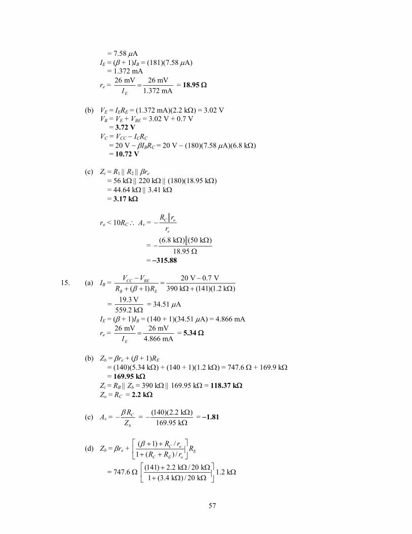
= 7.58 μA IE = (β + 1)IB = (181)(7.58 μA) = 1.372 mA
re = 26 mV 26 mV1.372 mAEI
= = 18.95 Ω
(b) VE = IERE = (1.372 mA)(2.2 kΩ) = 3.02 V VB = VE + VBE = 3.02 V + 0.7 V = 3.72 V VC = VCC − ICRC = 20 V − βIBRC = 20 V − (180)(7.58 μA)(6.8 kΩ) = 10.72 V (c) Zi = R1 || R2 || βre = 56 kΩ || 220 kΩ || (180)(18.95 kΩ) = 44.64 kΩ || 3.41 kΩ = 3.17 kΩ
ro < 10RC ∴ Av = C o
e
R rr
−
= (6.8 k ) (50 k )
18.95 Ω Ω
−Ω
= −315.88
15. (a) IB = 20 V 0.7 V ( 1) 390 k (141)(1.2 k )
CC BE
B E
V VR Rβ
− −=
+ + Ω + Ω
= 19.3 V559.2 kΩ
= 34.51 μA
IE = (β + 1)IB = (140 + 1)(34.51 μA) = 4.866 mA
re = 26 mV 26 mV4.866 mAEI
= = 5.34 Ω
(b) Zb = βre + (β + 1)RE = (140)(5.34 kΩ) + (140 + 1)(1.2 kΩ) = 747.6 Ω + 169.9 kΩ = 169.95 kΩ Zi = RB || Zb = 390 kΩ || 169.95 kΩ = 118.37 kΩ Zo = RC = 2.2 kΩ
(c) Av = C
b
RZβ
− = (140)(2.2 k )169.95 k
Ω−
Ω = −1.81
(d) Zb = βre + ( 1) /1 ( ) /
C oE
C E o
R r RR R r
β⎡ ⎤+ +⎢ ⎥+ +⎣ ⎦
= 747.6 Ω (141) 2.2 k / 20 k1 (3.4 k ) / 20 k
⎡ ⎤+ Ω Ω⎢ ⎥+ Ω Ω⎣ ⎦
1.2 kΩ
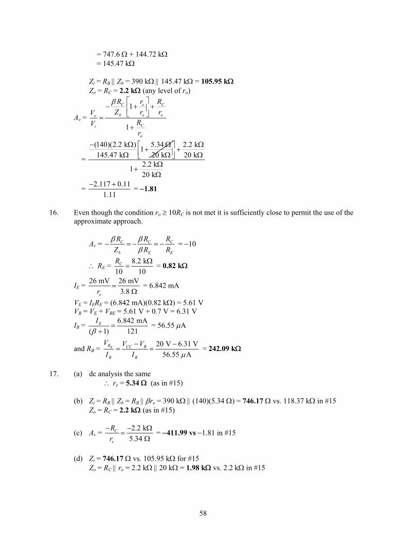
58
= 747.6 Ω + 144.72 kΩ = 145.47 kΩ Zi = RB || Zb = 390 kΩ || 145.47 kΩ = 105.95 kΩ Zo = RC = 2.2 kΩ (any level of ro)
Av = 1
1
C e C
b o oo
Ci
o
R r RZ r rV
RVr
β ⎡ ⎤− + +⎢ ⎥
⎣ ⎦=+
=
(140)(2.2 k ) 5.34 2.2 k1145.47 k 20 k 20 k
2.2 k120 k
− Ω Ω Ω⎡ ⎤+ +⎢ ⎥Ω Ω Ω⎣ ⎦Ω
+Ω
= 2.117 0.111.11
− + = −1.81
16. Even though the condition ro ≥ 10RC is not met it is sufficiently close to permit the use of the
approximate approach.
Av = C C C
b E E
R R RZ R Rβ β
β− = − = − = −10
∴ RE = 8.2 k10 10
CR Ω= = 0.82 kΩ
IE = 26 mV 26 mV3.8 er
=Ω
= 6.842 mA
VE = IERE = (6.842 mA)(0.82 kΩ) = 5.61 V VB = VE + VBE = 5.61 V + 0.7 V = 6.31 V
IB = 6.842 mA( 1) 121
EIβ
=+
= 56.55 μA
and RB = 20 V 6.31 V56.55 A
BR CC B
B B
V V VI I μ
− −= = = 242.09 kΩ
17. (a) dc analysis the same ∴ re = 5.34 Ω (as in #15) (b) Zi = RB || Zb = RB || βre = 390 kΩ || (140)(5.34 Ω) = 746.17 Ω vs. 118.37 kΩ in #15 Zo = RC = 2.2 kΩ (as in #15)
(c) Av = 2.2 k5.34
C
e
Rr− − Ω
=Ω
= −411.99 vs −1.81 in #15
(d) Zi = 746.17 Ω vs. 105.95 kΩ for #15 Zo = RC || ro = 2.2 kΩ || 20 kΩ = 1.98 kΩ vs. 2.2 kΩ in #15
59
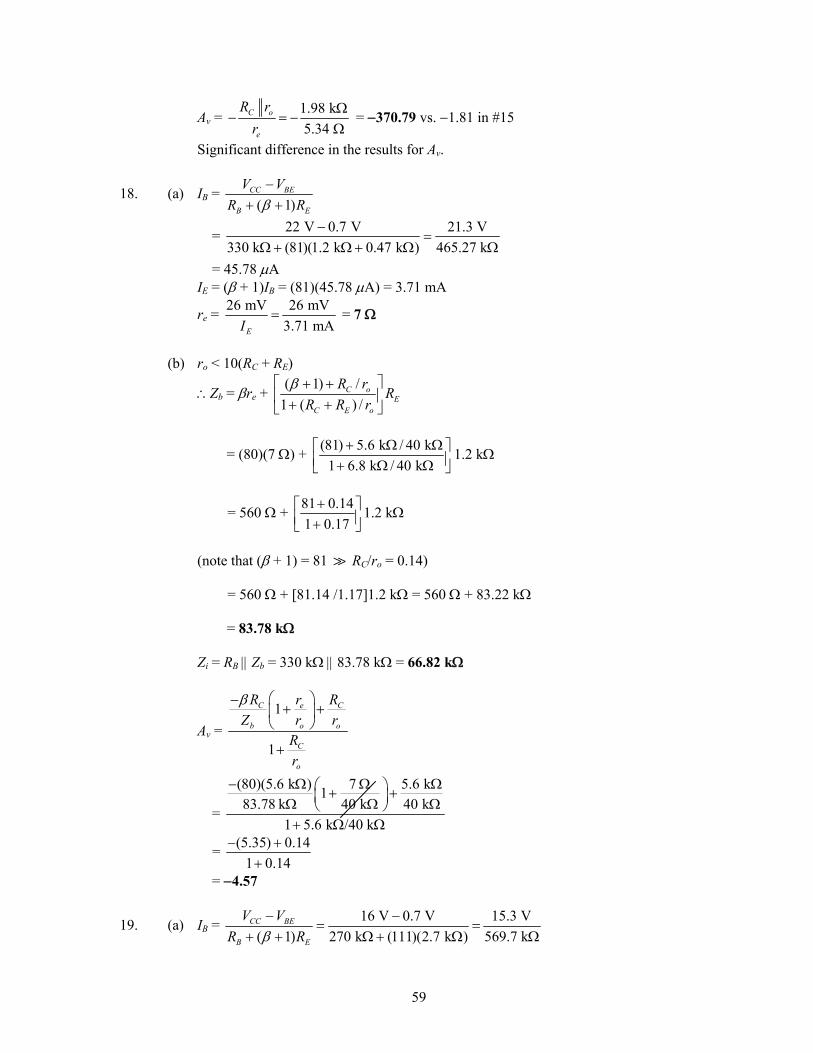
Av = 1.98 k5.34
C o
e
R rr
Ω− = −
Ω = −370.79 vs. −1.81 in #15
Significant difference in the results for Av.
18. (a) IB = ( 1)
CC BE
B E
V VR Rβ
−+ +
= 22 V 0.7 V 21.3 V330 k (81)(1.2 k 0.47 k ) 465.27 k
−=
Ω + Ω+ Ω Ω
= 45.78 μA IE = (β + 1)IB = (81)(45.78 μA) = 3.71 mA
re = 26 mV 26 mV3.71 mAEI
= = 7 Ω
(b) ro < 10(RC + RE)
∴Zb = βre + ( 1) /1 ( ) /
C oE
C E o
R r RR R r
β⎡ ⎤+ +⎢ ⎥+ +⎣ ⎦
= (80)(7 Ω) + (81) 5.6 k / 40 k1 6.8 k / 40 k
+ Ω Ω⎡ ⎤⎢ ⎥+ Ω Ω⎣ ⎦
1.2 kΩ
= 560 Ω + 81 0.141 0.17+⎡ ⎤
⎢ ⎥+⎣ ⎦1.2 kΩ
(note that (β + 1) = 81 RC/ro = 0.14)
= 560 Ω + [81.14 /1.17]1.2 kΩ = 560 Ω + 83.22 kΩ
= 83.78 kΩ
Zi = RB || Zb = 330 kΩ || 83.78 kΩ = 66.82 kΩ
Av = 1
1
C e C
b o o
C
o
R r RZ r r
Rr
β ⎛ ⎞−+ +⎜ ⎟
⎝ ⎠
+
=
(80)(5.6 k ) 7 5.6 k183.78 k 40 k 40 k
1 5.6 k /40 k
− Ω Ω Ω⎛ ⎞+ +⎜ ⎟Ω Ω Ω⎝ ⎠+ Ω Ω
= (5.35) 0.141 0.14
− ++
= −4.57
19. (a) IB = 16 V 0.7 V 15.3 V( 1) 270 k (111)(2.7 k ) 569.7 k
CC BE
B E
V VR Rβ
− −= =
+ + Ω + Ω Ω
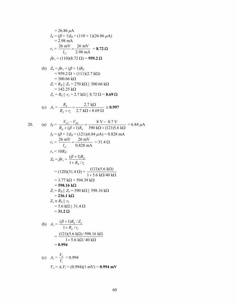
60
= 26.86 μA IE = (β + 1)IB = (110 + 1)(26.86 μA) = 2.98 mA
re = 26 mV 26 mV2.98 mAEI
= = 8.72 Ω
βre = (110)(8.72 Ω) = 959.2 Ω (b) Zb = βre + (β + 1)RE = 959.2 Ω + (111)(2.7 kΩ) = 300.66 kΩ Zi = RB || Zb = 270 kΩ || 300.66 kΩ = 142.25 kΩ Zo = RE || re = 2.7 kΩ || 8.72 Ω = 8.69 Ω
(c) Av = 2.7 k2.7 k 8.69
E
E e
RR r
Ω=
+ Ω + Ω ≅ 0.997
20. (a) IB = 8 V 0.7 V( 1) 390 k (121)5.6 k
CE BE
B E
V VR Rβ
− −=
+ + Ω + Ω = 6.84 μA
IE = (β + 1)IB = (121)(6.84 μA) = 0.828 mA
re = 26 mV 26 mV0.828 mAEI
= = 31.4 Ω
ro < 10RE:
Zb = βre + ( 1)1 /
E
E o
RR r
β ++
= (120)(31.4 Ω) + (121)(5.6 k )1 5.6 k /40 k
Ω+ Ω Ω
= 3.77 kΩ + 594.39 kΩ = 598.16 kΩ Zi = RB || Zb = 390 kΩ || 598.16 kΩ = 236.1 kΩ Zo ≅ RE || re
= 5.6 kΩ || 31.4 Ω
= 31.2 Ω
(b) Av = ( 1) /1 /
E b
E o
R ZR r
β ++
= (121)(5.6 k ) / 598.16 k1 5.6 k / 40 k
Ω Ω+ Ω Ω
= 0.994
(c) Av = 0
i
VV
= 0.994
Vo = AvVi = (0.994)(1 mV) = 0.994 mV
61
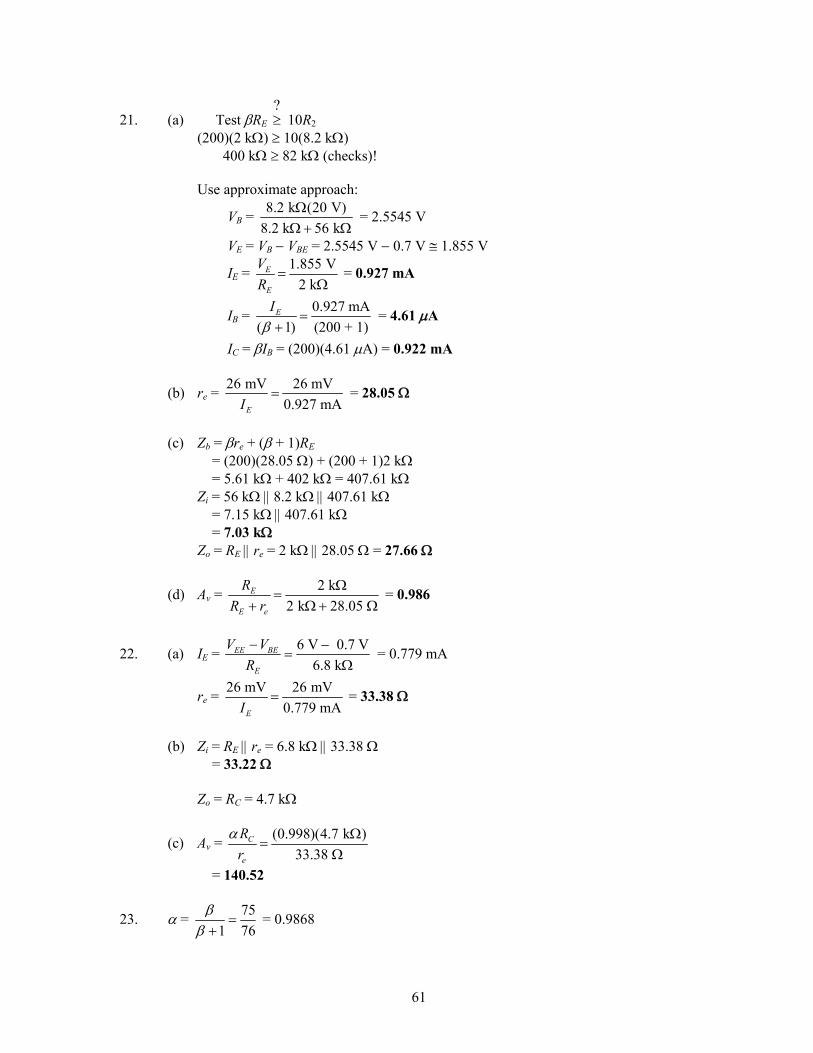
21. (a) Test βRE ?≥ 10R2
(200)(2 kΩ) ≥ 10(8.2 kΩ) 400 kΩ ≥ 82 kΩ (checks)! Use approximate approach:
VB = 8.2 k (20 V)8.2 k 56 k
ΩΩ+ Ω
= 2.5545 V
VE = VB − VBE = 2.5545 V − 0.7 V ≅ 1.855 V
IE = 1.855 V2 k
E
E
VR
=Ω
= 0.927 mA
IB = 0.927 mA( 1) (200 + 1)
EIβ
=+
= 4.61 μA
IC = βIB = (200)(4.61 μA) = 0.922 mA
(b) re = 26 mV 26 mV0.927 mAEI
= = 28.05 Ω
(c) Zb = βre + (β + 1)RE = (200)(28.05 Ω) + (200 + 1)2 kΩ = 5.61 kΩ + 402 kΩ = 407.61 kΩ Zi = 56 kΩ || 8.2 kΩ || 407.61 kΩ = 7.15 kΩ || 407.61 kΩ = 7.03 kΩ Zo = RE || re = 2 kΩ || 28.05 Ω = 27.66 Ω
(d) Av = 2 k2 k 28.05
E
E e
RR r
Ω=
+ Ω+ Ω = 0.986
22. (a) IE = 6 V 0.7 V6.8 k
EE BE
E
V VR− −
=Ω
= 0.779 mA
re = 26 mV 26 mV0.779 mAEI
= = 33.38 Ω
(b) Zi = RE || re = 6.8 kΩ || 33.38 Ω = 33.22 Ω Zo = RC = 4.7 kΩ
(c) Av = (0.998)(4.7 k )33.38
C
e
Rr
α Ω=
Ω
= 140.52
23. α = 751 76
ββ
=+
= 0.9868
62
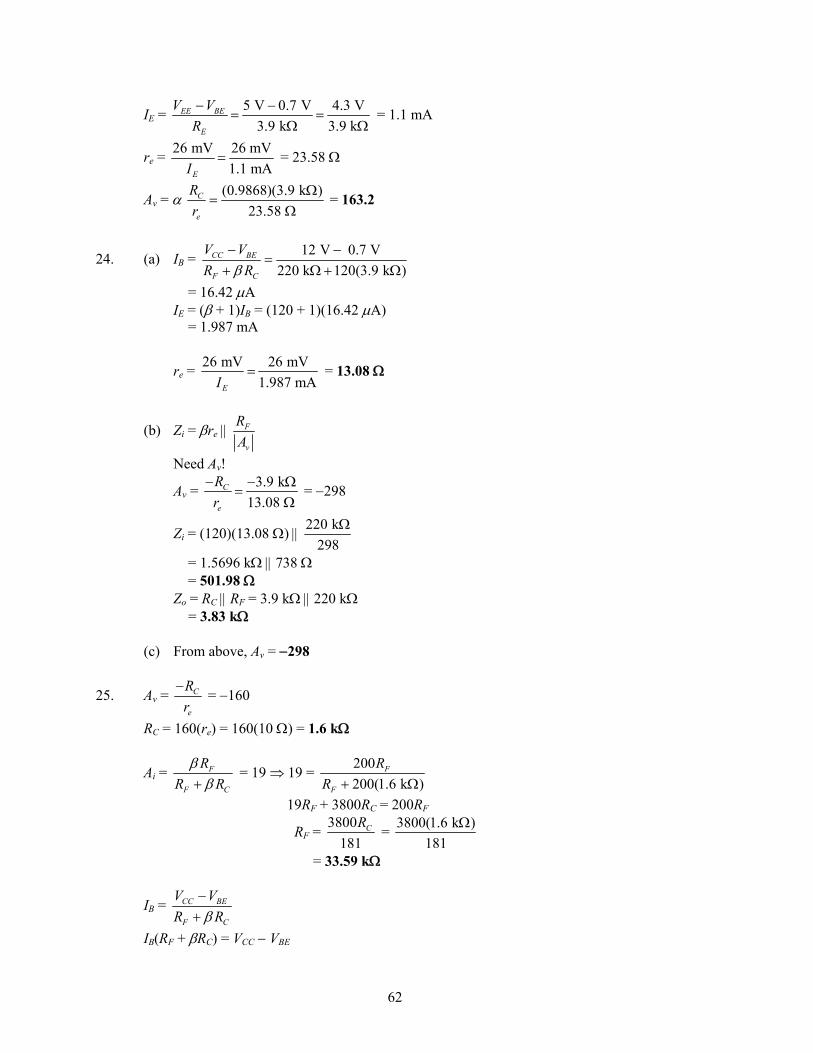
IE = 5 V 0.7 V 4.3 V3.9 k 3.9 k
EE BE
E
V VR− −
= =Ω Ω
= 1.1 mA
re = 26 mV 26 mV1.1 mAEI
= = 23.58 Ω
Av = α (0.9868)(3.9 k )23.58
C
e
Rr
Ω=
Ω = 163.2
24. (a) IB = 12 V 0.7 V220 k 120(3.9 k )
CC BE
F C
V VR Rβ
− −=
+ Ω + Ω
= 16.42 μA IE = (β + 1)IB = (120 + 1)(16.42 μA) = 1.987 mA
re = 26 mV 26 mV1.987 mAEI
= = 13.08 Ω
(b) Zi = βre || F
v
RA
Need Av!
Av = 3.9 k13.08
C
e
Rr− − Ω
=Ω
= −298
Zi = (120)(13.08 Ω) || 220 k298
Ω
= 1.5696 kΩ || 738 Ω = 501.98 Ω Zo = RC || RF = 3.9 kΩ || 220 kΩ = 3.83 kΩ (c) From above, Av = −298
25. Av = C
e
Rr− = −160
RC = 160(re) = 160(10 Ω) = 1.6 kΩ
Ai = F
F C
RR Rββ+
= 19 ⇒ 19 = 200200(1.6 k )
F
F
RR + Ω
19RF + 3800RC = 200RF
RF = 3800181
CR = 3800(1.6 k )181
Ω
= 33.59 kΩ
IB = CC BE
F C
V VR Rβ
−+
IB(RF + βRC) = VCC − VBE
63
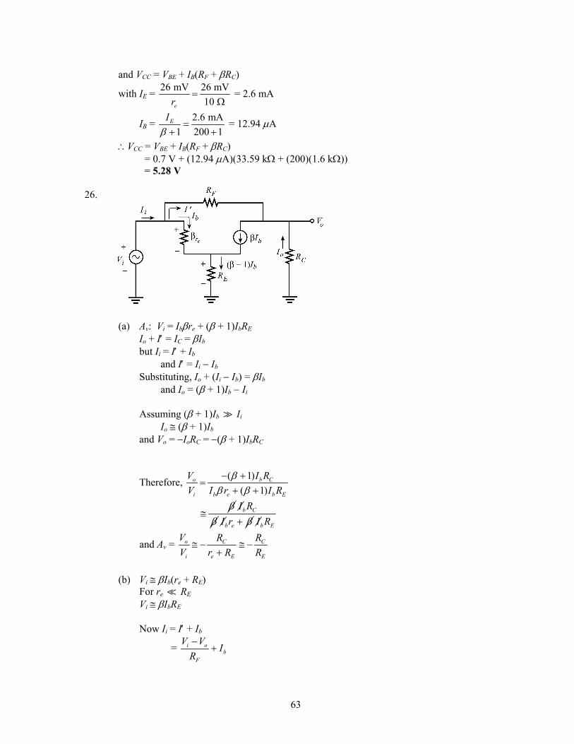
and VCC = VBE + IB(RF + βRC)
with IE = 26 mV 26 mV10 er
=Ω
= 2.6 mA
IB = 2.6 mA1 200 1
EIβ
=+ +
= 12.94 μA
∴VCC = VBE + IB(RF + βRC) = 0.7 V + (12.94 μA)(33.59 kΩ + (200)(1.6 kΩ)) = 5.28 V 26. (a) Av: Vi = Ibβre + (β + 1)IbRE
Io + I′ = IC = βIb but Ii = I′ + Ib and I′ = Ii − Ib Substituting, Io + (Ii − Ib) = βIb and Io = (β + 1)Ib − Ii Assuming (β + 1)Ib Ii Io ≅ (β + 1)Ib and Vo = −IoRC = −(β + 1)IbRC
Therefore, ( 1)( 1)
o b C
i b e b E
V I RV I r I R
ββ β− +
=+ +
b C
b e b E
I RI r I Rβ
β β≅
+
and Av = o C C
i e E E
V R RV r R R
≅ − ≅ −+
(b) Vi ≅ βIb(re + RE) For re RE Vi ≅ βIbRE Now Ii = I′ + Ib
= i ob
F
V V IR−
+
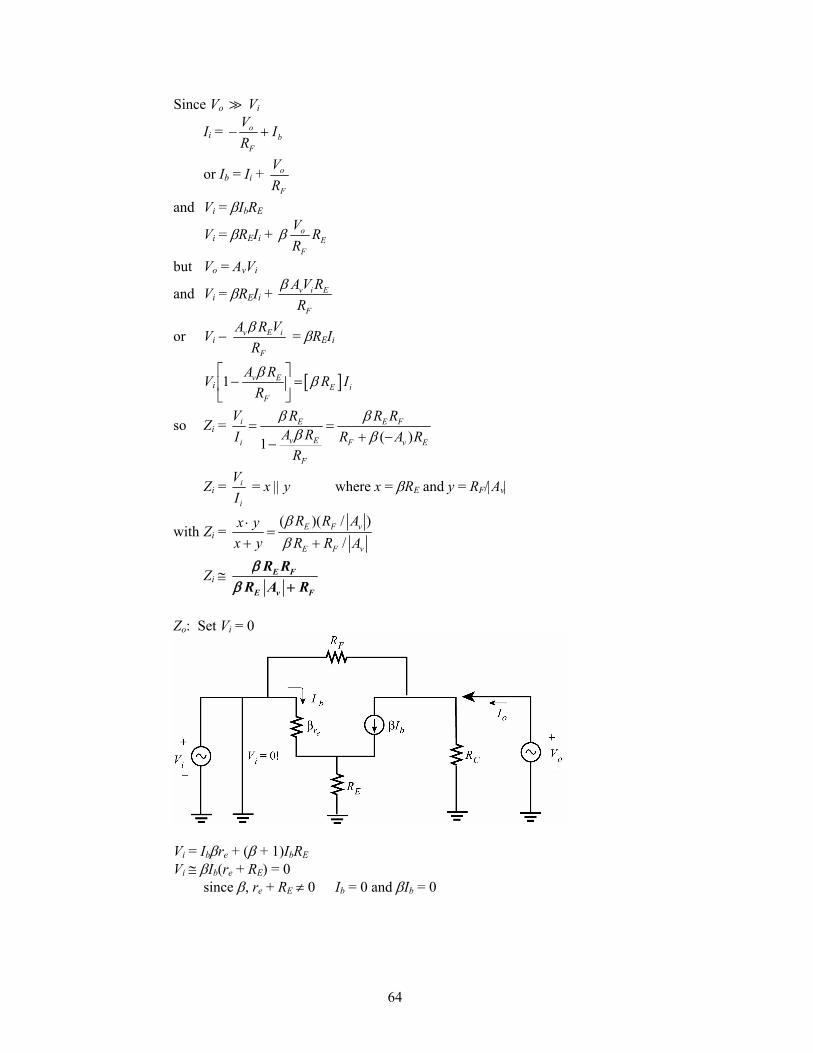
64
Since Vo Vi
Ii = ob
F
V IR
− +
or Ib = Ii + o
F
VR
and Vi = βIbRE
Vi = βREIi + oE
F
V RR
β
but Vo = AvVi
and Vi = βREIi + v i E
F
A V RR
β
or Vi − v E i
F
A R VRβ = βREIi
Vi [ ]1 v EE i
F
A R R IRβ
β⎡ ⎤− =⎢ ⎥
⎣ ⎦
so Zi = ( )1
i E E F
v Ei F v E
F
V R R RA RI R A R
R
β ββ β
= =+ −−
Zi = i
i
VI
= x || y where x = βRE and y = RF/|Av|
with Zi = ( )( / )
/E F v
E F v
R R Ax yx y R R A
ββ
⋅=
+ +
Zi ≅ ββ
E F
E v F
R RR A R+
Zo: Set Vi = 0
Vi = Ibβre + (β + 1)IbRE Vi ≅ βIb(re + RE) = 0 since β, re + RE ≠ 0 Ib = 0 and βIb = 0
65
∴ Io = 1 1o oo
C F C F
V V VR R R R
⎡ ⎤+ = +⎢ ⎥
⎣ ⎦
and Zo = 11 1
o C F
o C F
C F
V R RI R R
R R
= =++
= RC || RF
(c) Av ≅ 2.2 k1.2 k
C
E
RR
Ω− = −
Ω = −1.83
Zi ≅ (90)(1.2 k )(120 k )(90)(1.2 k )(1.83) 120 k
E F
E v F
R RR A Rβ
βΩ Ω
=+ Ω + Ω
= 40.8 kΩ Zo ≅ RC || RF = 2.2 kΩ || 120 kΩ = 2.16 kΩ
27. (a) IB = 9 V 0.7 V(39 k 22 k ) (80)(1.8 k )
CC BE
F C
V VR Rβ
− −=
+ Ω + Ω + Ω
= 8.3 V 8.3 V61 k 144 k 205 k
=Ω + Ω Ω
= 40.49 μA
IE = (β + 1)IB = (80 + 1)(40.49 μA) = 3.28 mA
re = 26 mV 26 mV3.28 mAEI
= = 7.93 Ω
Zi = 1FR || erβ
= 39 kΩ || (80)(7.93 Ω) = 39 kΩ || 634.4 Ω = 0.62 kΩ Zo = RC ||
2FR = 1.8 kΩ || 22 kΩ = 1.66 kΩ
(b) Av = 21.8 k 22 k
7.93 C F
e e
R RRr r
− Ω Ω′−= = −
Ω
= 1.664 k7.93
− ΩΩ
= −209.82
28. Ai ≅ β = 60 29. Ai ≅ β = 100 30. Ai = −AvZi/RC = −(−127.6)(1.768 kΩ)/3.9 kΩ = 57.85
31. (c) Ai = (140)(390 k )390 k 0.746 k
B
B b
RR Zβ Ω
=+ Ω + Ω
= 139.73
(d) Ai = iv
C
ZAR
− = −(−370.79)(746.17 Ω)/2.2 kΩ
= 125.76
66
32. Ai = −AvZi/RE = −(0.986)(7.03 kΩ)/2 kΩ = −3.47
33. Ai = o e
i e
I II I
α= = α = 0.9868 ≅ 1
34. Ai = −AvZi/RC = −(−298)(501.98 Ω)/3.9 kΩ = 38.37
35. Ai = ( 209.82)(0.62 k )1.8 k
iv
C
ZAR
− − Ω− =
Ω = 72.27
36. (a) IB = 18 V 0.7 V680 k
CC BE
B
V VR− −
=Ω
= 25.44 μA
IE = (β + 1)IB = (100 + 1)(25.44 μA) = 2.57 mA
re = 26 mV2.57 mA
= 10.116 Ω
3.3 k10.116 NL
Cv
e
RAr
Ω= − = −
Ω = −326.22
Zi = RB || βre = 680 kΩ || (100)(10.116 Ω) = 680 kΩ || 1,011.6 Ω = 1.01 kΩ Zo = RC = 3.3 kΩ (b) −
(c) LvA = 4.7 k
4.7 k 3.3 kNL
Lv
L o
R AR R
Ω=
+ Ω + Ω(−326.22)
= −191.65
(d) Li
A = (1.01 k )( 191.65)4.7 kL
iv
L
ZAR
Ω− = − −
Ω
= 41.18
(e) LvA =
( ) 100(1.939 k )( ) 100(10.116 )
b C Lo
i b e
I R RVV I r
ββ
− − Ω= =
Ω
= −191.98 Zi = RB || βre = 1.01 kΩ
IL = ( )C b
C L
R IR R
β+
= 41.25Ib
Ib = B i
B e
R IR rβ+
= 0.9985Ii
Li
A = o bL L
i i b i
I II II I I I= = ⋅ = (41.25)(0.9985)
= 41.19 Zo = RC = 3.3 kΩ
67
37. (a) NLvA = −326.22
LvA =
NL
Lv
L o
R AR R+
RL = 4.7 kΩ: LvA = 4.7 k ( 326.22)
4.7 k 3.3 kΩ
−Ω+ Ω
= −191.65
RL = 2.2 kΩ: LvA = 2.2 k ( 326.22)
2.2 k 3.3 kΩ
−Ω+ Ω
= −130.49
RL = 0.5 kΩ: LvA = 0.5 k ( 326.22)
0.5 k 2.3 kΩ
−Ω+ Ω
= −42.92
As RL↓, LvA ↓
(b) No change for Zi, Zo, and
NLvA !
38. (a) IB = 12 V 0.7 V1 M
CC BE
B
V VR− −
=Ω
= 11.3 μA
IE = (β + 1)IB = (181)(11.3 μA) = 2.045 mA
re = 26 mV 26 mV2.045 mAEI
= = 12.71 Ω
NLVA = 3 k
12.71 C
e
Rr
Ω− = −
Ω = −236
Zi = RB || βre = 1 MΩ || (180)(12.71 Ω) = 1 MΩ || 2.288 kΩ = 2.283 kΩ Zo = RC = 3 kΩ (b) − (c) No-load: Av =
NLvA = −236
(d) 2.283 k ( 236)2.283 k 0.6 ks NL
iv v
i s
ZA AZ R
Ω −= =
+ Ω + Ω
= −186.9 (e) Vo = −IoRC = −βIbRC Vi = Ibβre
Av = 3 k12.71
o b C C
i b e e
V I R RV I r r
ββ
Ω= − = − = −
Ω = −236
s
o o iv
s i s
V V VAV V V
= = ⋅
Vi = (1 M ) 2.288 k ( )
(1 M ) 2.288 k 0.6 ke s s
e s
r V Vr Rββ
Ω Ω=
Ω + Ω+ Ω = 0.792 Vs
svA = (−236)(0.792)
= −186.9 (same results)
68
(f) No change!
(g) 2.283 k ( 236)( )2.283 k 1 ks NL
iv v
i s
ZA AZ R
Ω −= =
+ Ω + Ω = −164.1
Rs↑, svA ↓
(h) No change!
39. (a) IB = 24 V 0.7 V500 k
CC BE
B
V VR− −
=Ω
= 41.61 μA
IE = (β + 1)IB = (80 + 1)(41.61 μA) = 3.37 mA
re = 26 mV 26 mV3.37 mAEI
= = 7.715 Ω
NLvA = 4.3 k
7.715 L
e
Rr
Ω− = −
Ω = −557.36
Zi = RB || βre = 560 kΩ || (80)(7.715 Ω) = 560 kΩ || 617.2 Ω = 616.52 Ω Zo = RC = 4.3 kΩ (b) −
(c) LvA = 2.7 k ( 557.36)
2.7 k 4.3 kNL
o Lv
i L o
V R AV R R
Ω −= =
+ Ω + Ω
= −214.98
s
o o iv
s i s
V V VAV V V
= = ⋅
Vi = 616.52 616.52 1 k
i s s
i s
Z V VZ R
Ω=
+ Ω + Ω = 0.381 Vs
( 214.98)(0.381)svA = −
= −81.91
(d) 1 k 616.52 ( 81.91)2.7 ks s
s ii v
L
R ZA AR
⎛ ⎞+ Ω + Ω⎛ ⎞= − = − −⎜ ⎟ ⎜ ⎟Ω⎝ ⎠⎝ ⎠
= 49.04
(e) LvA = 5.6 k ( 557.36)
5.6 k 4.3 kNL
o Lv
i L o
V R AV R R
Ω −= =
+ Ω + Ω = −315.27
i
s
VV
the same = 0.381
s
o iv
i s
V VAV V
= ⋅ = (−315.27)(0.381) = −120.12
As RL↑, svA ↑
69
(f) LvA the same = −214.98
616.52 616.52 0.5 k
i i
s i s
V ZV Z R
Ω= =
+ Ω + Ω = 0.552
s
o iv
i s
V VAV V
= ⋅ = (−214.98)(0.552) = −118.67
As Rs↓, svA ↑
(g) No change! 40. (a) Exact analysis:
ETh = 2
1 2
16 k (16 V)68 k 16 kCC
R VR R
Ω=
+ Ω + Ω = 3.048 V
RTh = R1 || R2 = 68 kΩ || 16 kΩ = 12.95 kΩ
IB = 3.048 V 0.7 V( 1) 12.95 k (101)(0.75 k )
Th BE
Th E
E VR Rβ
− −=
+ + Ω + Ω
= 26.47 μA IE = (β + 1)IB = (101)(26.47 μA) = 2.673 mA
re = 26 mV 26 mV2.673 mAEI
= = 9.726 Ω
2.2 k9.726 NL
Cv
e
RAr− Ω
= = −Ω
= −226.2
Zi = 68 kΩ || 16 kΩ || βre = 12.95 kΩ || (100)(9.726 Ω) = 12.95 kΩ || 972.6 Ω = 904.66 Ω Zo = RC = 2.2 kΩ (b) −
(c) LvA = 5.6 k ( 226.2)( )
5.6 k 2.2 kNL
Lv
L o
R AR Z
Ω −=
+ Ω + Ω = −162.4
(d) Li
A = L
iv
L
ZAR
−
= −(−162.4) (904.66 )5.6 k
ΩΩ
= 26.24
70
(e) LvA =
2.2 k 5.6 k9.726
C e
e
R Rr
− − Ω Ω=
Ω
= −162.4 Zi = 68 kΩ || 16 kΩ || 972.6 Ω βre
= 904.66 Ω
Li
A = L
iv
L
ZAR
−
= ( 162.4)(904.66 )5.6 k
− ΩΩ
= 26.24 Zo = RC = 2.2 kΩ Same results!
41. (a) LvA =
NL
Lv
L o
R AR Z+
RL = 4.7 kΩ: LvA = 4.7 k ( 226.4)
4.7 k 2.2 kΩ
−Ω+ Ω
= −154.2
RL = 2.2 kΩ: LvA = 2.2 k ( 226.4)
2.2 k 2.2 kΩ
−Ω+ Ω
= −113.2
RL = 0.5 kΩ: LvA = 0.5 k ( 226.4)
0.5 k 2.2 kΩ
−Ω + Ω
= −41.93
RL↓, LvA ↓
(b) Unaffected!
42. (a) IB = 18 V 0.7 V( 1) 680 k (111)(0.82 k )
CC BE
B E
V VR Rβ
− −=
+ + Ω + Ω
= 22.44 μA IE = (β + 1)IB = (110 + 1)(22.44 μA) = 2.49 mA
re = 26 mV 26 mV2.49 mAEI
= = 10.44 Ω
3 k10.44 0.82 kNL
Cv
e E
RAr R
Ω= − = −
+ Ω + Ω
= −3.61 Zi ≅ RB || Zb = 680 kΩ || (βre + (β + 1)RE) = 680 kΩ || (610)(10.44 Ω) + (110 + 1)(0.82 kΩ) = 680 kΩ || 92.17 kΩ = 81.17 kΩ Zo ≅ RC = 3 kΩ (b) −
71
(c) LvA = 4.7 k ( 3.61)
4.7 k 3 kNL
o Lv
i L o
V R AV R R
Ω −= =
+ Ω + Ω
= −2.2
s
o o iv
s i s
V V VAV V V
= = ⋅
Vi = 81.17 k ( )81.17 k 0.6 k
i s s
i s
Z V VZ R
Ω=
+ Ω + Ω = 0.992 Vs
svA = (−2.2)(0.992)
= −2.18 (d) None! (e)
LvA – none!
81.17 k81.17 k 1 k
i i
s i s
V ZV Z R
Ω= =
+ Ω + Ω = 0.988
svA = (−2.2)(0.988)
= −2.17 Rs↑,
svA ↓, (but only slightly for moderate changes in Rs since Zi is typically much larger than Rs)
43. Using the exact approach:
IB = ( 1)
Th BE
Th E
E VR Rβ
−+ +
ETh = 2
1 2CC
R VR R+
= 2.33 V 0.7 V10.6 k (121)(1.2 k )
−Ω + Ω
= 12 k (20 V)91 k 12 k
ΩΩ+ Ω
= 2.33 V
= 10.46 μA RTh = R1 || R2 = 91 kΩ || 12 kΩ = 10.6 kΩ IE = (β + 1)IB = (121)(10.46 μA) = 1.266 mA
re = 26 mV 26 mV1.266 mAEI
= = 20.54 Ω
(a) 1.2 k20.54 1.2 kNL
Ev
e E
RAr R
Ω≅ =
+ Ω + Ω = 0.983
Zi = R1 || R2 || (βre + (β +1)RE) = 91 kΩ || 12 kΩ || ((120)(20.54 Ω) + (120 + 1)(1.2 kΩ)) = 10.6 kΩ || (2.46 kΩ + 145.2 kΩ) = 10.6 kΩ || 147.66 kΩ = 9.89 kΩ Zo = RE || re = 1.2 kΩ || 20.54 Ω = 20.19 Ω
72
(b) −
(c) LvA = 2.7 k (0.983)
2.7 k 20.19 NL
Lv
L o
R AR Z
Ω=
+ Ω + Ω
= 0.976
9.89 k (0.976)9.89 k 0.6 ks L
iv v
i s
ZA AZ R
Ω= =
+ Ω+ Ω
= 0.92 (d)
LvA = 0.976 (unaffected by change in Rs)
9.89 k (0.976)9.89 k 1 ks L
iv v
i s
ZA AZ R
Ω= =
+ Ω+ Ω
= 0.886 (vs. 0.92 with Rs = 0.6 kΩ) As Rs↑,
svA ↓ (e) Changing Rs will have no effect on
NLvA , Zi, or Zo.
(f) LvA = ( ) 5.6 k (0.983)
5.6 k 20.19 NL
Lv
L o
R AR Z
Ω=
+ Ω + Ω
= 0.979 (vs. 0.976 with RL = 2.7 kΩ)
9.89 k (0.979)( )9.89 k 0.6 ks L
iv v
i s
ZA AZ R
Ω= =
+ Ω+ Ω
= 0.923 (vs. 0.92 with RL = 2.7 kΩ) As RL↑,
LvA ↑, svA ↑
44. (a) IE = 6 V 0.7 V2.2 k
EE BE
E
V VR− −
=Ω
= 2.41 mA
re = 26 mV 26 mV2.41 mAEI
= = 10.79 Ω
NLvA = 4.7 k
10.79 C
e
Rr
Ω=
Ω = 435.59
Zi = RE || re = 2.2 kΩ || 10.79 Ω = 10.74 Ω Zo = RC = 4.7 kΩ (b) −
(c) LvA = 5.6 k (435.59)
5.6 k 4.7 kNL
Lv
L o
R AR R
Ω=
+ Ω + Ω = 236.83
Vi = 10.74 ( )10.74 100
i ss
i s
Z VVZ R
Ω=
+ Ω + Ω = 0.097 Vs
s
o iv
i s
V VAV V
= ⋅ = (236.83)(0.097)
= 22.97
73
(d) Vi = Ie ⋅ re Vo = −IoRL
Io = 4.7 k ( )4.7 k 5.6 k
eI− ΩΩ+ Ω
= −0.4563Ie
LvA = o
i
VV
= (0.4563 ) 0.4563(5.6 k )10.79
e L
e e
I RI r
+ Ω=
⋅ Ω
= 236.82 (vs. 236.83 for part c) :
svA 2.2 kΩ || 10.79 Ω = 10.74 Ω
Vi = 10.74 ( )10.74 100
i ss
i s
Z VVZ R
Ω⋅ =
+ Ω + Ω = 0.097 Vs
s
o iv
i s
V VAV V
= ⋅ = (236.82)(0.097)
= 22.97 (same results)
(e) LvA = 2.2 k (435.59)
2.2 k 4.7 kNL
Lv
L o
R AR R
Ω=
+ Ω + Ω
= 138.88
0 10.74 ,10.74 500 s
i i iv
i s s i s
V V V ZAV V V Z R
Ω= ⋅ = =
+ Ω + Ω = 0.021
svA = (138.88)(0.021) = 2.92
svA very sensitive to increase in Rs due to relatively small Zi; Rs↑,
svA ↓
LvA sensitive to RL; RL↓, LvA ↓
(f) Zo = RC = 4.7 kΩ unaffected by value of Rs! (g) Zi = RE || re = 10.74 Ω unaffected by value of RL!
45. (a) 1
1 k ( 420)1 k 3.3 k
NLL vv
L o
R AA
R RΩ −
= =+ Ω + Ω
= −97.67
2
2.7 k ( 420)2.7 k 3.3 k
NLL vv
L o
R AA
R RΩ −
= =+ Ω + Ω
= −189
(b)
LvA = 1 2v vA A⋅ = (−97.67)(−189) = 18.46 × 10³
1 1
2 1
s
o io ov
s i i s
V VV VAV V V V
= = ⋅ ⋅
= 2 1
iv v
s
VA AV
⋅ ⋅
Vi = 1 k ( )1 k 0.6 k
i s s
i s
Z V VZ R
Ω=
+ Ω + Ω = 0.625
svA = (−189)(−97.67)(0.625)
= 11.54 × 10³
74
(c) 1
( 97.67)(1 k )1 k
v ii
L
A ZAR
− − Ω= − =
Ω = 97.67
2
( 189)(1 k )2.7 k
v ii
L
A ZAR
− − − Ω= =
Ω = 70
(d)
1 2Li i iA A A= ⋅ = (97.67)(70) = 6.84 × 10³ (e) No effect! (f) No effect! (g) In phase
46. (a) 2
1 1
2 1
1.2 k (1)1.2 k 20 NL
iv v
i o
ZA A
Z ZΩ
= =+ Ω + Ω
= 0.984
2vA =
2
2
2.2 k ( 640)2.2 k 4.6 kNL
Lv
L o
R AR Z
Ω= −
+ Ω + Ω
= −207.06 (b)
1 2Lv v vA A A= ⋅ = (0.984)(−207.06) = −203.74
s L
iv v
i s
ZA AZ R
=+
= 50 k ( 203.74)50 k 1 k
Ω−
Ω + Ω
= −199.75
(c) 1
1 1
2
ii v
i
ZA A
Z= −
= (50 k )(0.984)1.2 k
Ω−
Ω
= −41
2
2 2
ii v
L
ZA A
R= −
= (1.2 k )( 207.06)2.2 k
Ω− −
Ω
= 112.94
(d) 1
L L
ii v
L
ZA A
R= −
= −(−203.74) (50 k )2.2 k
ΩΩ
= 4.63 × 10³
75
(e) A load on an emitter-follower configuration will contribute to the emitter resistance (in fact, lower the value) and therefore affect Zi (reduce its magnitude).
(f) The fact that the second stage is a CE amplifier will isolate Zo from the first stage and Rs. (g) The emitter-follower has zero phase shift while the common-emitter amplifier has a
180° phase shift. The system, therefore, has a total phase shift of 180° as noted by the negative sign in front of the gain for
TvA in part b. 47. For each stage:
VB = 6.2 k24 k 6.2 k
ΩΩ+ Ω
(15 V) = 3.08 V
VE = VB − 0.7 V = 3.08 V − 0.7 V = 2.38 V
IE ≅ IC = 2.38 V1.5 k
E
E
VR
=Ω
= 1.59 mA
VC = VCC − ICRC = 15 V − (1.59 mA)(5.1 kΩ) = 6.89 V
48. re = 26 mV 26 mV1.59 mAEI
= = 16.35 Ω
2i
R = R1 || R2 || βre = 6.2 kΩ || 24 kΩ || (150)(16.35 Ω) = 1.64 kΩ
2
1
5.1 k 1.64 k16.35
C iv
e
R RA
rΩ Ω
= − =Ω
= −75.8
2
5.1 k16.35
Cv
e
RAr
− Ω= − =
Ω = −311.9
Av = 1 2v vA A = (−75.8)(−311.9) = 23,642
49. 1
3.9 k (20 V)3.9 k 6.2 k 7.5 kBV Ω
=Ω + Ω+ Ω
= 4.4 V
2
6.2 k 3.9 k (20 V)3.9 k 6.2 k 7.5 kBV Ω+ Ω
=Ω + Ω + Ω
= 11.48 V
1 1E BV V= − 0.7 V = 4.4 V − 0.7 V = 3.7 V
1
1 1
3.7 V1 k
EC E
E
VI I
R≅ = =
Ω = 3.7 mA ≅
2 2E CI I≅
2CV = VCC − ICRC = 20 V − (3.7 mA)(1.5 kΩ)
= 14.45 V
76
50. re = 26 mV 26 mV3.7 mAEI
= = 7 Ω
1
ev
e
rAr
= − = −1
2
1.5 k7
Ev
e
RAr
Ω= =
Ω ≅ 214
1 2Tv v vA A A= = (−1)(214) = −214
Vo = Tv iA V = (−214)(10 mV) = −2.14 V
51. Ro = RD = 1.5 kΩ (Vo (from problem 50) = −2.14 V)
Vo(load) = 10 k( ) ( 2.14 V)10 k 1.5 k
Lo
o L
R VR R
Ω= −
+ Ω + Ω
= −1.86 V
52. IB = (16 V 1.6 V)(6000)(510 ) 2.4 M
CC BE
D E B
V VR Rβ− −
=+ Ω + Ω
= 14.4 V5.46 MΩ
= 2.64 μA
IC ≅ IE = βDIB = 6000(2.64 μA) = 15.8 mA VE = IERE = (15.8 mA)(510 Ω) = 8.06 V 53. From problem 69, IE = 15.8 mA
re = 26 26 V15.8 mAEI
= = 1.65 Ω
Av = 510 1.65 510
E
e E
Rr R
Ω=
+ Ω + Ω = 0.997 ≈ 1
54. dc: 16 V 1.6 V2.4 M (6000)(510 )
CC BEB
B D E
V VIR Rβ
− −≅ =
+ Ω+ Ω = 2.64 μA
(6000)(2.64 A)C D BI Iβ μ= = = 15.84 mA
2
2
26 mV 26 mV15.84 mAe
E
rI
= = = 1.64 Ω
ac:
2(6000)(1.64 ) 9.84 ki D eZ rβ≅ = Ω = Ω
1 9.84 k
ib
VI =Ω
1( )( ) (6000) (200 )
9.84 k= 121.95
io D b C
VV I R
Vi
β⎛ ⎞
= − = − Ω⎜ ⎟Ω⎝ ⎠−
and ov
i
VAV
= ≅ −121.95
77
55. IB = 1
1 2
16 V 0.7 V1.5 M (160)(200)(100 )
CC EB
B E
V VR Rβ β
− −=
+ Ω + Ω
= 3.255 μA IC ≅ β1β2IB = (160)(200)(3.255μA) ≅ 104.2 mA
2CV = VCC − ICRC = 16 V − (104.2 mA)(100 Ω) = 5.58 V
1BV = IBRB = (3.255 μA)(1.5 MΩ) = 4.48 V 56. From problem 55:
1EI = 0.521 mA
1
26 mV 26 mV (mA) 0.521 mAe
E
rI
= = = 49.9 Ω
1 ii eR rβ= = 160(49.9 Ω) = 7.98 kΩ
Av = 1
1 2
1 2
(160)(200)(100 )(160)(200)(100 ) 7.98 k
C
C i
RR R
β ββ β
Ω=
+ Ω + Ω
= 0.9925 Vo = AvVi = 0.9975 (120 mV) = 119.7 mV
57. re = (dc)
26 mV 26 mV1.2 mAEI
= = 21.67 Ω
βre = (120)(21.67 Ω) = 2.6 kΩ 58. − 59. − 60. − 61. −
62. (a) Av = o
i
VV
= −160
Vo = −160 Vi
(b) Ib = (1 )i re o i re v i i re v
ie ie ie
V h V V h A V V h Ah h h− − −
= =
= ( )41 (2 10 )(160)
1 kiV −− ×
Ω
Ib = 9.68 × 10⁻⁴Vi
(c) Ib = 1 k
iVΩ
= 1 × 10⁻³Vi
78
(d) % Difference = 3 4
3
1 10 9.68 101 10
i i
i
V VV
− −
−
× − ××
× 100%
= 3.2 % (e) Valid first approximation
63. % difference in total load = 1/L L oe
L
R R hR
− × 100%
= 2.2 k (2.2 k 50 k )
2.2 kΩ− Ω Ω
Ω × 100%
= 2.2 k 2.1073 k2.2 k
Ω− ΩΩ
× 100%
= 4.2 % In this case the effect of 1/hoe can be ignored. 64. (a) Vo = −180Vi (hie = 4 kΩ, hre = 4.05 × 10⁻⁴)
(b) Ib = 4(4.05 10 )(180 )
4 ki iV V−− ×
Ω
= 2.32 × 10⁻⁴Vi
(c) Ib = 4 k
i i
ie
V Vh
=Ω
= 2.5 × 10⁻⁴Vi
(d) % Difference = 4 4
4
2.5 10 2.32 102.5 10
i i
i
V VV
− −
−
× − ××
× 100% = 7.2%
(e) Yes, less than 10% 65. From Fig. 5.18
min max hoe: 1 μS 30 μS Avg = (1 30) S
2μ+ = 15.5 μS
66. (a) hfe = β = 120 hie ≅ βre = (120)(4.5 Ω) = 540 Ω
hoe = 1 140 kor
=Ω
= 25 μS
(b) re ≅ 1 k90
iehβ
Ω= = 11.11 Ω
β = hfe = 90
ro = 1 120 Soeh μ
=
= 50 kΩ
79
67. (a) re = 8.31 Ω (from problem 9) (b) feh = β = 60
ieh = βre = (60)(8.31 Ω) = 498.6 Ω (c) Zi = RB || hie = 220 kΩ || 498.6 Ω = 497.47 Ω Zo = RC = 2.2 kΩ
(d) Av = (60)(2.2 k )498.6
fe C
ie
h Rh
− − Ω=
Ω = −264.74
Ai ≅ hfe = 60 (e) Zi = 497.47 Ω (the same)
Zo = ro || RC, ro = 125 Sμ
= 40 kΩ
= 40 kΩ || 2.2 kΩ = 2.09 kΩ
(f) Av = ( ) (60)(2.085 k )
498.6 fe o C
ie
h r Rh
− − Ω=
Ω = −250.90
Ai = −AvZi/RC = −(−250.90)(497.47 Ω)/2.2 kΩ = 56.73 68. (a) 68 kΩ || 12 kΩ = 10.2 kΩ Zi = 10.2 kΩ || hie = 10.2 kΩ || 2.75 kΩ = 2.166 kΩ Zo = RC || ro = 2.2 kΩ || 40 kΩ = 2.085 kΩ
(b) Av = fe C
ie
h Rh
′− CR′ = RC || ro = 2.085 kΩ
= (180)(2.085 k )2.75 k
− ΩΩ
= −136.5
Ai = o o i
i i i
I I II I I
′= ⋅
′
= 10.2 k1 10.2 k 2.68 k
ef
oe L
hh R
⎛ ⎞ Ω⎛ ⎞⎜ ⎟⎜ ⎟+ Ω+ Ω⎝ ⎠⎝ ⎠
= 180 (0.792)1 (25 S)(2.2 k )μ⎛ ⎞⎜ ⎟+ Ω⎝ ⎠
= 135.13
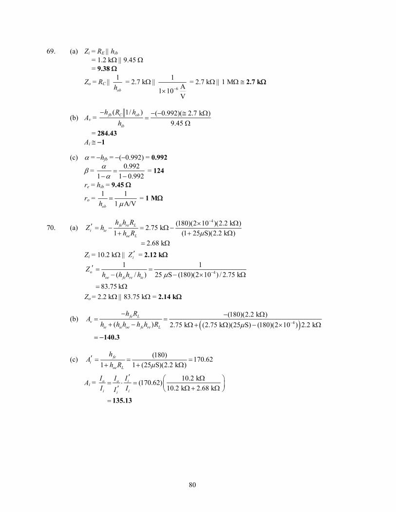
80
69. (a) Zi = RE || hib = 1.2 kΩ || 9.45 Ω = 9.38 Ω
Zo = RC || 1
obh = 2.7 kΩ ||
6
1A1 10V
−× = 2.7 kΩ || 1 MΩ ≅ 2.7 kΩ
(b) Av = ( 1/ ) ( 0.992)( 2.7 k )
9.45 fb C ob
ib
h R hh
− − − ≅ Ω=
Ω
= 284.43 Ai ≅ −1 (c) α = −hfb = −(−0.992) = 0.992
β = 0.9921 1 0.992αα=
− − = 124
re = hib = 9.45 Ω
ro = 1 11 A/Vobh μ
= = 1 MΩ
70. (a) 4(180)(2 10 )(2.2 k )2.75 k
1 (1 25 S)(2.2 k )fe re L
i ieoe L
h h RZ h
h R μ
−× Ω′ = − = Ω−+ + Ω
2.68 k= Ω Zi = 10.2 kΩ || iZ ′ = 2.12 kΩ
4
1 1( / ) 25 S (180)(2 10 ) / 2.75 k
83.75 k
ooe fe re ie
Zh h h h μ −
′ = =− − × Ω
= Ω
Zo = 2.2 kΩ || 83.75 kΩ = 2.14 kΩ
(b) ( )4
(180)(2.2 k )( ) 2.75 k (2.75 k )(25 S) (180)(2 10 ) 2.2 k
fe Lv
ie ie oe fe re L
h RA
h h h h h R μ −
− − Ω= =
+ − Ω+ Ω − × Ω
= 140.3−
(c) (180) 170.621 1 (25 S)(2.2 k )
fei
oe L
hA
h R μ′ = = =
+ + Ω
Ai = 10.2 k(170.62)10.2 k 2.68 k
o o i
i ii
I I II II
′ Ω⎛ ⎞= ⋅ = ⎜ ⎟Ω + Ω′ ⎝ ⎠
= 135.13
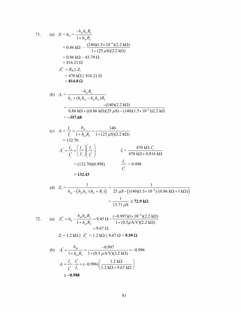
81
71. (a) Zi = hie = 1
fe re L
oe L
h h Rh R
−
+
= 0.86 kΩ − 4(140)(1.5 10 )(2.2 k )
1 (25 S)(2.2 k )μ
−× Ω+ Ω
= 0.86 kΩ − 43.79 Ω = 816.21 Ω iZ ′ = RB || Zi = 470 kΩ || 816.21 Ω = 814.8 Ω
(b) Av = ( )
fe L
ie ie oe fe re L
h Rh h h h h R
−
+ −
= 4
(140)(2.2 k )0.86 k ((0.86 k )(25 S) (140)(1.5 10 ))2.2 kμ −
− ΩΩ + Ω − × Ω
= −357.68
(c) Ai = 1401 1 (25 S)(2.2 k )
feo
i oe L
hII h R μ= =
+ + Ω
= 132.70
o o ii
ii i
I I IAII I
⎛ ⎞⎛ ⎞′ ⎜ ⎟= = ⎜ ⎟⎜ ⎟′ ′⎝ ⎠⎝ ⎠ Ii = 470 k
470 k 0.816 kiI ′Ω
Ω + Ω
= (132.70)(0.998) i
i
I
I ′ = 0.998
= 132.43
(d) Zo = ( )
1/( )oe fe re ie sh h h h R− +
= ( )4
125 S (140)(1.5 10 ) /(0.86 k 1 k )μ −− × Ω + Ω
= 113.71 Sμ
≅ 72.9 kΩ
72. (a) 4( 0.997)(1 10 )(2.2 k )9.45
1 1 (0.5 A/V)(2.2 k )fb rb L
i ibob L
h h RZ h
h R μ
−− × Ω′ = − = Ω −+ + Ω
9.67 = Ω Zi = 1.2 kΩ || iZ ′ = 1.2 kΩ || 9.67 Ω = 9.59 Ω
(b) 0.997 0.9961 1 (0.5 A/V)(2.2 k )
fbi
ob L
hA
h R μ−′ = = = −
+ + Ω
1.2 k( 0.996)1.2 k 9.67 k
o ii
ii
I IAII
′ Ω⎛ ⎞= ⋅ = − ⎜ ⎟Ω + Ω′ ⎝ ⎠
≅ 0.988−
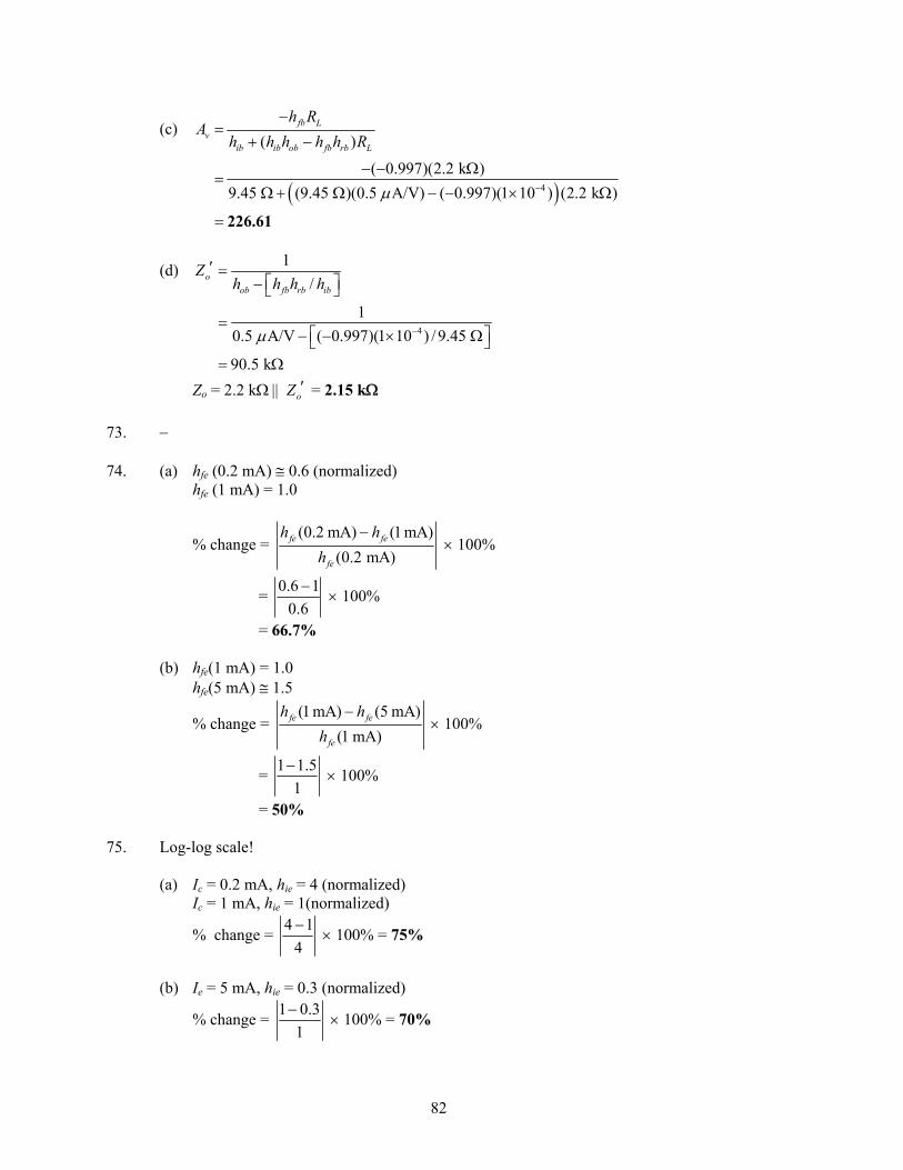
82
(c)
( )4
( )
( 0.997)(2.2 k )9.45 (9.45 )(0.5 A/V) ( 0.997)(1 10 ) (2.2 k )
fb Lv
ib ib ob fb rb L
h RA
h h h h h R
μ −
−=
+ −
− − Ω=
Ω + Ω − − × Ω
= 226.61
(d)
4
1/
10.5 A/V ( 0.997)(1 10 ) / 9.45
90.5 k
oob fb rb ib
Zh h h h
μ −
′ =⎡ ⎤− ⎣ ⎦
=⎡ ⎤− − × Ω⎣ ⎦
= Ω
Zo = 2.2 kΩ || oZ ′ = 2.15 kΩ 73. − 74. (a) hfe (0.2 mA) ≅ 0.6 (normalized) hfe (1 mA) = 1.0
% change = (0.2 mA) (1 mA)
(0.2 mA)fe fe
fe
h hh
− × 100%
= 0.6 10.6− × 100%
= 66.7% (b) hfe(1 mA) = 1.0 hfe(5 mA) ≅ 1.5
% change = (1 mA) (5 mA)
(1 mA)fe fe
fe
h hh
− × 100%
= 1 1.51− × 100%
= 50% 75. Log-log scale! (a) Ic = 0.2 mA, hie = 4 (normalized) Ic = 1 mA, hie = 1(normalized)
% change = 4 14− × 100% = 75%
(b) Ie = 5 mA, hie = 0.3 (normalized)
% change = 1 0.31− × 100% = 70%
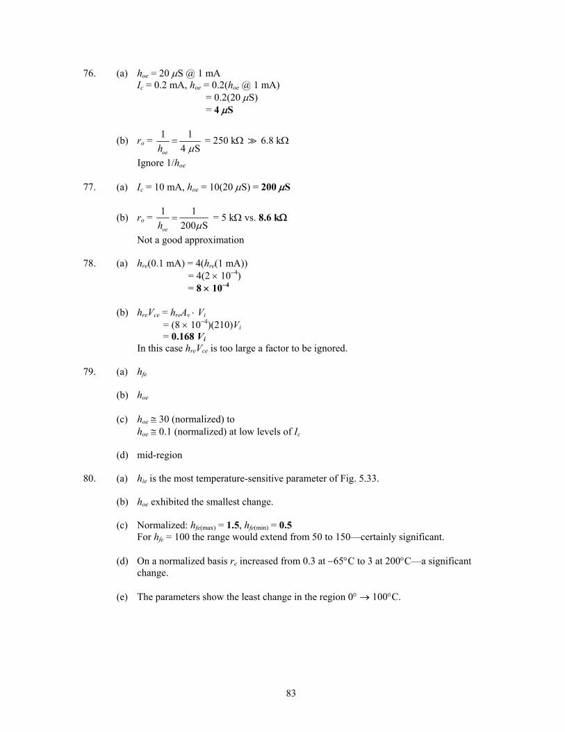
83
76. (a) hoe = 20 μS @ 1 mA Ic = 0.2 mA, hoe = 0.2(hoe @ 1 mA) = 0.2(20 μS) = 4 μS
(b) ro = 1 14 Soeh μ
= = 250 kΩ 6.8 kΩ
Ignore 1/hoe 77. (a) Ic = 10 mA, hoe = 10(20 μS) = 200 μS
(b) ro = 1 1200 Soeh μ
= = 5 kΩ vs. 8.6 kΩ
Not a good approximation 78. (a) hre(0.1 mA) = 4(hre(1 mA)) = 4(2 × 10⁻⁴) = 8 × 10⁻⁴ (b) hreVce = hreAv ⋅ Vi = (8 × 10⁻⁴)(210)Vi = 0.168 Vi In this case hreVce is too large a factor to be ignored. 79. (a) hfe (b) hoe (c) hoe ≅ 30 (normalized) to hoe ≅ 0.1 (normalized) at low levels of Ic (d) mid-region 80. (a) hie is the most temperature-sensitive parameter of Fig. 5.33. (b) hoe exhibited the smallest change. (c) Normalized: hfe(max) = 1.5, hfe(min) = 0.5 For hfe = 100 the range would extend from 50 to 150—certainly significant. (d) On a normalized basis re increased from 0.3 at −65°C to 3 at 200°C—a significant
change. (e) The parameters show the least change in the region 0° → 100°C.
84
81. (a) Test: βRE ≥ 10R2 70(1.5 kΩ) ≥ 10(39 kΩ)
105 kΩ ?≥ 390 kΩ
No! RTh = 39 kΩ || 150 kΩ = 30.95 kΩ
ETh = 39 k (14 V)39 k 150 k
ΩΩ+ Ω
= 2.89 V
IB = 2.89 V 0.7 V( 1) 30.95 k (71)(1.5 k )
Th BE
Th E
E VR Rβ
− −=
+ + Ω + Ω
= 15.93 μA VB = ETh − IBRTh = 2.89 V − (15.93 μA)(30.95 kΩ) = 2.397 V VE = 2.397 V − 0.7 V = 1.697 V
and IE = 1.697 V1.5 k
E
E
VR
=Ω
= 1.13 mA
VCE = VCC − IC(RC + RE) = 14 V − 1.13 mA(2.2 kΩ + 1.5 kΩ) = 9.819 V Biasing OK (b) R2 not connected at base:
IB = 0 14 V 0.7 V( 1) 150 k + (71)(1.5 k )CC
B E
VR Rβ
− −=
+ + Ω Ω = 51.85 μA
VB = VCC − IBRB = 14 V − (51.85 μA)(150 kΩ) = 6.22 V as noted in Fig. 5.187.
85
Eq. (6.1) is valid!
Chapter 6 1. − 2. From Fig. 6.11: VGS = 0 V, ID = 8 mA VGS = −1 V, ID = 4.5 mA VGS = −1.5 V, ID = 3.25 mA VGS = −1.8 V, ID = 2.5 mA VGS = −4 V, ID = 0 mA VGS = −6 V, ID = 0 mA 3. (a) VDS ≅ 1.4 V
(b) rd = 1.4 V6 mA
VI= = 233.33 Ω
(c) VDS ≅ 1.6 V
(d) rd = 1.6 V3 mA
VI= = 533.33 Ω
(e) VDS ≅ 1.4 V
(f) rd = 1.4 V1.5 mA
VI= = 933.33 Ω
(g) ro = 233.33 Ω
rd = [ ] [ ]2 2
233.33 233.33 0.56251 1 ( 1 V) ( 4 V)
o
GS P
rV V
Ω Ω= =
− − − −
= 414.81 Ω
(h) rd = [ ]2
233.33 233.33 0.251 ( 2 V) ( 4 V)
Ω Ω=
− − − = 933.2 Ω
(i) 533.33 Ω vs. 414.81 Ω 933.33 Ω vs 933.2 Ω 4. (a) VGS = 0 V, ID = 8 mA (for VDS > VP) VGS = −1 V, ID = 4.5 mA ΔID = 3.5 mA (b) VGS = −1 V, ID = 4.5 mA VGS = −2 V, ID = 2 mA ΔID = 2.5 mA
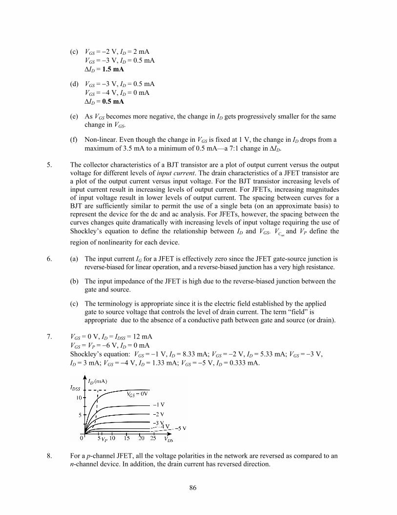
86
(c) VGS = −2 V, ID = 2 mA VGS = −3 V, ID = 0.5 mA ΔID = 1.5 mA (d) VGS = −3 V, ID = 0.5 mA VGS = −4 V, ID = 0 mA ΔID = 0.5 mA (e) As VGS becomes more negative, the change in ID gets progressively smaller for the same
change in VGS. (f) Non-linear. Even though the change in VGS is fixed at 1 V, the change in ID drops from a
maximum of 3.5 mA to a minimum of 0.5 mA—a 7:1 change in ΔID. 5. The collector characteristics of a BJT transistor are a plot of output current versus the output
voltage for different levels of input current. The drain characteristics of a JFET transistor are a plot of the output current versus input voltage. For the BJT transistor increasing levels of input current result in increasing levels of output current. For JFETs, increasing magnitudes of input voltage result in lower levels of output current. The spacing between curves for a BJT are sufficiently similar to permit the use of a single beta (on an approximate basis) to represent the device for the dc and ac analysis. For JFETs, however, the spacing between the curves changes quite dramatically with increasing levels of input voltage requiring the use of Shockley’s equation to define the relationship between ID and VGS. satCV and VP define the region of nonlinearity for each device.
6. (a) The input current IG for a JFET is effectively zero since the JFET gate-source junction is
reverse-biased for linear operation, and a reverse-biased junction has a very high resistance. (b) The input impedance of the JFET is high due to the reverse-biased junction between the
gate and source. (c) The terminology is appropriate since it is the electric field established by the applied
gate to source voltage that controls the level of drain current. The term “field” is appropriate due to the absence of a conductive path between gate and source (or drain).
7. VGS = 0 V, ID = IDSS = 12 mA VGS = VP = −6 V, ID = 0 mA Shockley’s equation: VGS = −1 V, ID = 8.33 mA; VGS = −2 V, ID = 5.33 mA; VGS = −3 V, ID = 3 mA; VGS = −4 V, ID = 1.33 mA; VGS = −5 V, ID = 0.333 mA.
8. For a p-channel JFET, all the voltage polarities in the network are reversed as compared to an
n-channel device. In addition, the drain current has reversed direction.
87
9. (b) IDSS = 10 mA, VP = −6 V 10. VGS = 0 V, ID = IDSS = 12 mA VGS = VP = −4 V, ID = 0 mA
VGS = 2PV = −2 V, ID =
4DSSI = 3 mA
VGS = 0.3VP = −1.2 V, ID = 6 mA VGS = −3 V, ID = 0.75 mA (Shockley’s equation) 11. (a) ID = IDSS = 9 mA (b) ID = IDSS(1 − VGS/VP)2 = 9 mA(1 − (−2 V)/(−3.5 V))2 = 1.653 mA (c) VGS = VP = −3.5 V, ID = 0 mA (d) VGS < VP = −3.5 V, ID = 0 mA 12. VGS = 0 V, ID = 16 mA VGS = 0.3VP = 0.3(−5 V) = −1.5 V, ID = IDSS/2 = 8 mA VGS = 0.5VP = 0.5(−5 V) = −2.5 V, ID = IDSS/4 = 4 mA VGS = VP = −5 V, ID = 0 mA 13. VGS = 0 V, ID = IDSS = 7.5 mA VGS = 0.3VP = (0.3)(4 V) = 1.2 V, ID = IDSS/2 = 7.5 mA/2 = 3.75 mA VGS = 0.5VP = (0.5)(4 V) = 2 V, ID = IDSS/4 = 7.5 mA/4 = 1.875 mA VGS = VP = 4 V, ID = 0 mA 14. (a) ID = IDSS(1 − VGS/VP)2 = 6 mA(1 − (−2 V)/(−4.5 V))2 = 1.852 mA ID = IDSS(1 − VGS/VP)2 = 6 mA(1 − (−3.6 V)/(−4.5 V))2 = 0.24 mA
(b) VGS = 3 mA1 ( 4.5 V) 16 mA
DP
DSS
IVI
⎛ ⎞ ⎛ ⎞− = − −⎜ ⎟ ⎜ ⎟⎜ ⎟⎜ ⎟
⎝ ⎠⎝ ⎠
= −1.318 V
VGS = 5.5 mA1 ( 4.5 V) 16 mA
DP
DSS
IVI
⎛ ⎞ ⎛ ⎞− = − −⎜ ⎟ ⎜ ⎟⎜ ⎟⎜ ⎟
⎝ ⎠⎝ ⎠
= −0.192 V 15. ID = IDSS(1 − VGS/VP)2 3 mA = IDSS(1 − (−3 V)/(−6 V))2 3 mA = IDSS(0.25) IDSS = 12 mA
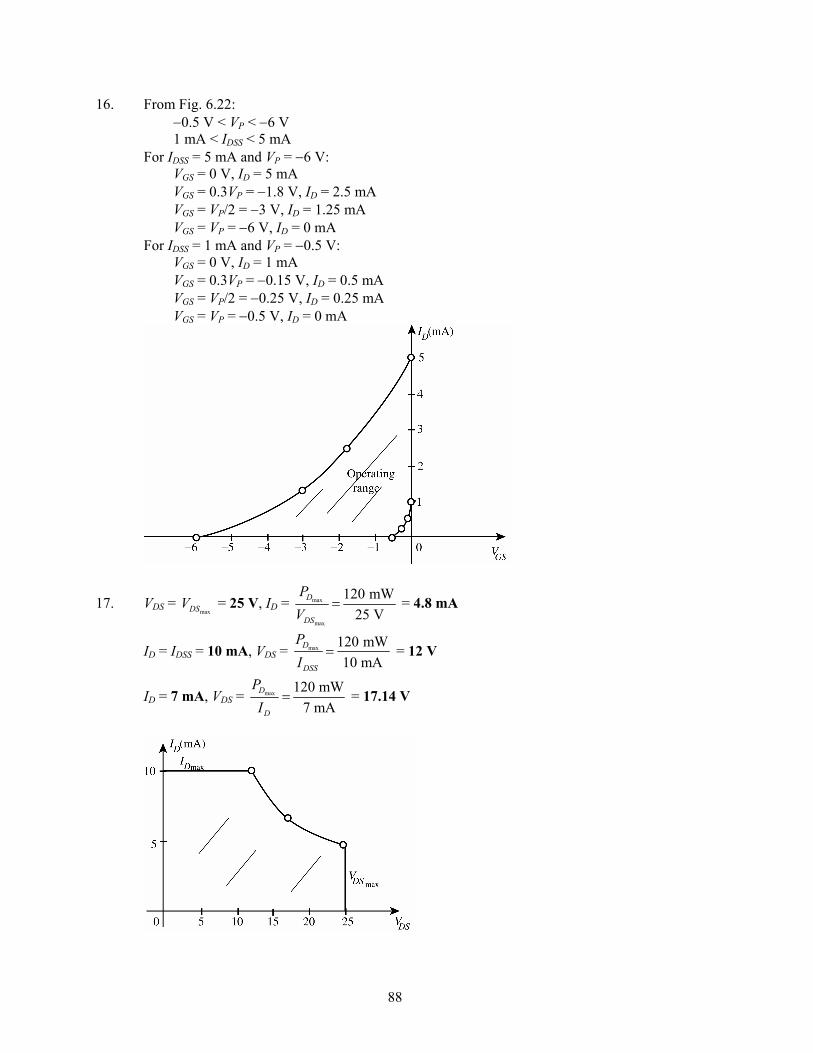
88
16. From Fig. 6.22: −0.5 V < VP < −6 V 1 mA < IDSS < 5 mA For IDSS = 5 mA and VP = −6 V: VGS = 0 V, ID = 5 mA VGS = 0.3VP = −1.8 V, ID = 2.5 mA VGS = VP/2 = −3 V, ID = 1.25 mA VGS = VP = −6 V, ID = 0 mA For IDSS = 1 mA and VP = −0.5 V: VGS = 0 V, ID = 1 mA VGS = 0.3VP = −0.15 V, ID = 0.5 mA VGS = VP/2 = −0.25 V, ID = 0.25 mA VGS = VP = −0.5 V, ID = 0 mA
17. VDS = maxDSV = 25 V, ID = max
max
120 mW25 V
D
DS
PV
= = 4.8 mA
ID = IDSS = 10 mA, VDS = max 120 mW10 mA
D
DSS
PI
= = 12 V
ID = 7 mA, VDS = max 120 mW7 mA
D
D
PI
= = 17.14 V
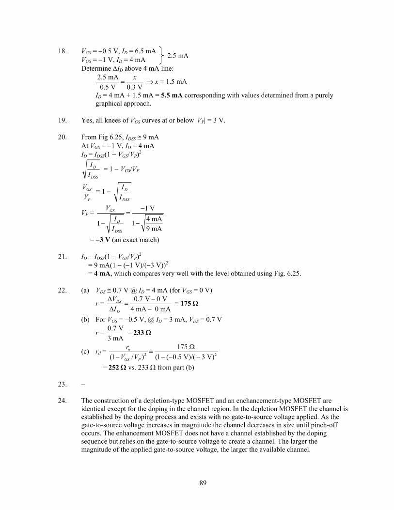
89
2.5 mA18. VGS = −0.5 V, ID = 6.5 mA VGS = −1 V, ID = 4 mA Determine ΔID above 4 mA line:
2.5 mA0.5 V 0.3 V
x= ⇒ x = 1.5 mA
ID = 4 mA + 1.5 mA = 5.5 mA corresponding with values determined from a purely graphical approach.
19. Yes, all knees of VGS curves at or below |VP| = 3 V. 20. From Fig 6.25, IDSS ≅ 9 mA At VGS = −1 V, ID = 4 mA ID = IDSS(1 − VGS/VP)2
D
DSS
II
= 1 − VGS/VP
GS
P
VV
= 1 − D
DSS
II
VP = 1 V4 mA119 mA
GS
D
DSS
VI
I
−=
−−
= −3 V (an exact match) 21. ID = IDSS(1 − VGS/VP)2 = 9 mA(1 − (−1 V)/(−3 V))2 = 4 mA, which compares very well with the level obtained using Fig. 6.25. 22. (a) VDS ≅ 0.7 V @ ID = 4 mA (for VGS = 0 V)
r = 0.7 V 0 V4 mA 0 mA
DS
D
VI
Δ −=
Δ − = 175 Ω
(b) For VGS = −0.5 V, @ ID = 3 mA, VDS = 0.7 V
r = 0.7 V3 mA
= 233 Ω
(c) rd = 2 2
175 (1 / ) (1 ( 0.5 V)/( 3 V)
o
GS P
rV V
Ω=
− − − −
= 252 Ω vs. 233 Ω from part (b) 23. − 24. The construction of a depletion-type MOSFET and an enchancement-type MOSFET are
identical except for the doping in the channel region. In the depletion MOSFET the channel is established by the doping process and exists with no gate-to-source voltage applied. As the gate-to-source voltage increases in magnitude the channel decreases in size until pinch-off occurs. The enhancement MOSFET does not have a channel established by the doping sequence but relies on the gate-to-source voltage to create a channel. The larger the magnitude of the applied gate-to-source voltage, the larger the available channel.
90
DIΔ = 3.34 mA
DIΔ = 4.67 mA
DIΔ = 6 mA
25. − 26. At VGS = 0 V, ID = 6 mA At VGS = −1 V, ID = 6 mA(1 − (−1 V)/(−3 V))2 = 2.66 mA At VGS = +1 V, ID = 6 mA(1 − (+1 V)/(−3 V))2 = 6 mA(1.333)2 = 10.667 mA At VGS = +2 V, ID = 6 mA(1 − (+2 V)/(−3 V))2 = 6 mA(1.667)2 = 16.67 mA
From −1 V to 0 V, ΔID = 3.34 mA while from +1 V to +2 V, ΔID = 6 mA − almost a 2:1 margin. In fact, as VGS becomes more and more positive, ID will increase at a faster and faster
rate due to the squared term in Shockley’s equation.
27. VGS = 0 V, ID = IDSS = 12 mA; VGS = −8 V, ID = 0 mA; VGS = 2PV = −4 V, ID = 3 mA;
VGS = 0.3VP = −2.4 V, ID = 6 mA; VGS = −6 V, ID = 0.75 mA 28. From problem 20:
VP = 1 V 1 V 1 V1 1.2139514 mA 1 1.47311
9.5 mA
GS
D
DSS
VI
I
+ + += = =
−−−−
= 10.21395−
≅ −4.67 V
29. ID = IDSS(1 − VGS/VP)2
IDSS = ( )2 2
4 mA(1 ( 2 V) ( 5 V))1
D
GS P
IV V
=− − −−
= 11.11 mA
30. From problem 14(b):
VGS = 20 mA1 ( 5 V) 12.9 mA
DP
DSS
IVI
⎛ ⎞ ⎛ ⎞− = − −⎜ ⎟ ⎜ ⎟⎜ ⎟⎜ ⎟
⎝ ⎠⎝ ⎠
= (−5 V)(1 − 2.626) = (−5 V)(−1.626) = 8.13 V 31. From Fig. 6.34,
maxDP = 200 mW, ID = 8 mA P = VDSID
and VDS = max 200 mW8 mAD
PI
= = 25 V
VGS ID
−1 V 2.66 mA 0 6.0 mA
+1 V 10.67 mA +2 V 16.67 mA
91
32. (a) In a depletion-type MOSFET the channel exists in the device and the applied voltage VGS controls the size of the channel. In an enhancement-type MOSFET the channel is not established by the construction pattern but induced by the applied control voltage VGS.
(b) − (c) Briefly, an applied gate-to-source voltage greater than VT will establish a channel
between drain and source for the flow of charge in the output circuit. 33. (a) ID = k(VGS − VT)2 = 0.4 × 10⁻³(VGS − 3.5)2
VGS ID 3.5 V 0
4 V 0.1 mA 5 V 0.9 mA 6 V 2.5 mA 7 V 4.9 mA 8 V 8.1 mA
(b) ID = 0.8 × 10⁻³(VGS − 3.5)2
VGS ID 3.5 V 0
4 V 0.2 mA 5 V 1.8 mA 6 V 5.0 mA 7 V 9.8 mA 8 V 16.2 mA
For same levels of VGS, ID attains twice the current level as part (a). Transfer curve has steeper slope. For both curves, ID = 0 mA for VGS < 3.5 V.
34. (a) k = ( )
(on)2 2
(on)
4 mA(6 V 4 V)
D
GS T
I
V V=
−− = 1 mA/V2
ID = k(VGS − VT)2 = 1 × 10⁻³(VGS − 4 V)2
(b) VGS ID For VGS < VT = 4 V, ID = 0 mA 4 V 0 mA 5 V 1 mA 6 V 4 mA 7 V 9 mA 8 V 16 mA
(c) VGS ID (VGS < VT) 2 V 0 mA 5 V 1 mA 10 V 36 mA
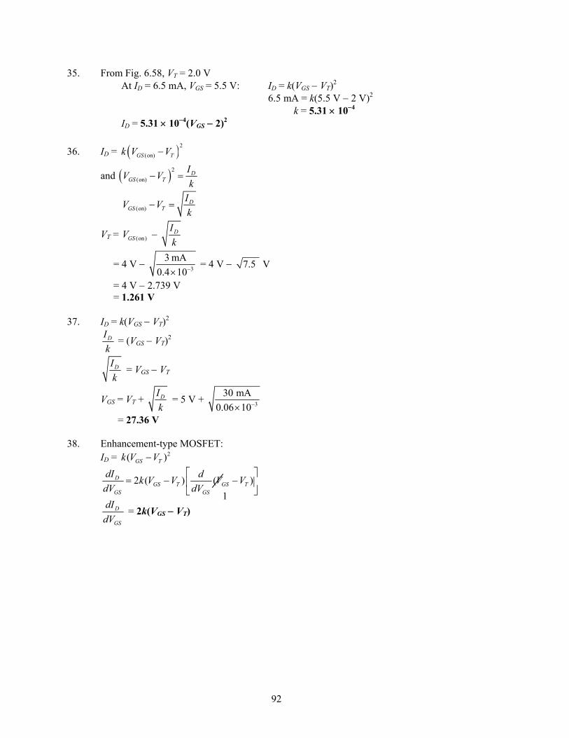
92
35. From Fig. 6.58, VT = 2.0 V At ID = 6.5 mA, VGS = 5.5 V: ID = k(VGS − VT)2 6.5 mA = k(5.5 V − 2 V)2 k = 5.31 × 10⁻⁴ ID = 5.31 × 10⁻⁴(VGS − 2)2 36. ID = ( )2
(on)GS Tk V V−
and ( )2
(on)D
GS TIV Vk
− =
(on)D
GS TIV Vk
− =
VT = (on)GSV − DIk
= 4 V − 3
3 mA0.4 10−×
= 4 V − 7.5 V
= 4 V − 2.739 V = 1.261 V 37. ID = k(VGS − VT)2
DIk
= (VGS − VT)2
DIk
= VGS − VT
VGS = VT + DIk
= 5 V + 3
30 mA0.06 10−×
= 27.36 V 38. Enhancement-type MOSFET: ID = 2( )GS Tk V V−
2 ( ) ( )DGS T GS T
GS GS
dI dk V V V VdV dV
⎡ ⎤= − −⎢ ⎥
⎣ ⎦
D
GS
dIdV
= 2k(VGS − VT) 1
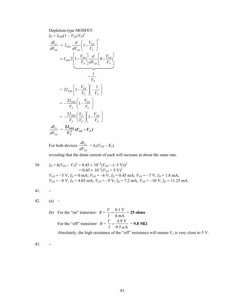
93
Depletion-type MOSFET: ID = IDSS(1 − VGS/VP)2
D
GS
dIdV
= 2
1 GSDSS
GS P
VdIdV V
⎛ ⎞−⎜ ⎟
⎝ ⎠
2 1 0GS GSDSS
P GS P
V d VIV dV V
⎡ ⎤ ⎡ ⎤= − −⎢ ⎥ ⎢ ⎥
⎣ ⎦ ⎣ ⎦
1
PV−
= 12 1 GSDSS
P P
VIV V
⎛ ⎞⎛ ⎞− −⎜ ⎟⎜ ⎟
⎝ ⎠⎝ ⎠
= 2 1DSS GS
P P
I VV V
⎛ ⎞− −⎜ ⎟
⎝ ⎠
= 2 1DSS GSP
P P P
I VVV V V
⎛ ⎞⎛ ⎞− −⎜ ⎟⎜ ⎟
⎝ ⎠⎝ ⎠
D
GS
dIdV
= 2
2 ( )DSSGS P
P
I V VV
−
For both devices D
GS
dIdV
= k1(VGS − K2)
revealing that the drain current of each will increase at about the same rate. 39. ID = k(VGS − VT)2 = 0.45 × 10⁻³(VGS − (−5 V))2 = 0.45 × 10⁻³(VGS + 5 V)2 VGS = −5 V, ID = 0 mA; VGS = −6 V, ID = 0.45 mA; VGS = −7 V, ID = 1.8 mA; VGS = −8 V, ID = 4.05 mA; VGS = −9 V, ID = 7.2 mA; VGS = −10 V, ID = 11.25 mA 41. − 42. (a) −
(b) For the “on” transistor: R = 0.1 V4 mA
VI= = 25 ohms
For the “off” transistor: R = 4.9 V0.5 A
VI μ= = 9.8 MΩ
Absolutely, the high resistance of the “off” resistance will ensure Vo is very close to 5 V. 43. −
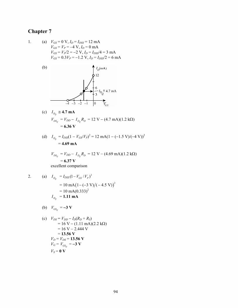
94
Chapter 7 1. (a) VGS = 0 V, ID = IDSS = 12 mA VGS = VP = −4 V, ID = 0 mA VGS = VP/2 = −2 V, ID = IDSS/4 = 3 mA VGS = 0.3VP = −1.2 V, ID = IDSS/2 = 6 mA (b) (c)
QDI ≅ 4.7 mA
QDSV = VDD −
QD DI R = 12 V − (4.7 mA)(1.2 kΩ)
= 6.36 V (d)
QDI = IDSS(1 − VGS/VP)2 = 12 mA(1 − (−1.5 V)/(−4 V))2
= 4.69 mA
QDSV = VDD − QD DI R = 12 V − (4.69 mA)(1.2 kΩ)
= 6.37 V excellent comparison 2. (a)
QDI = IDSS2(1 / )GS PV V−
= 10 mA ( )21 ( 3 V) ( 4.5 V)− − − = 10 mA(0.333)2
QDI = 1.11 mA (b)
QGSV = −3 V (c) VDS = VDD − ID(RD + RS) = 16 V − (1.11 mA)(2.2 kΩ) = 16 V − 2.444 V = 13.56 V VD = VDS = 13.56 V VG =
QGSV = −3 V
VS = 0 V
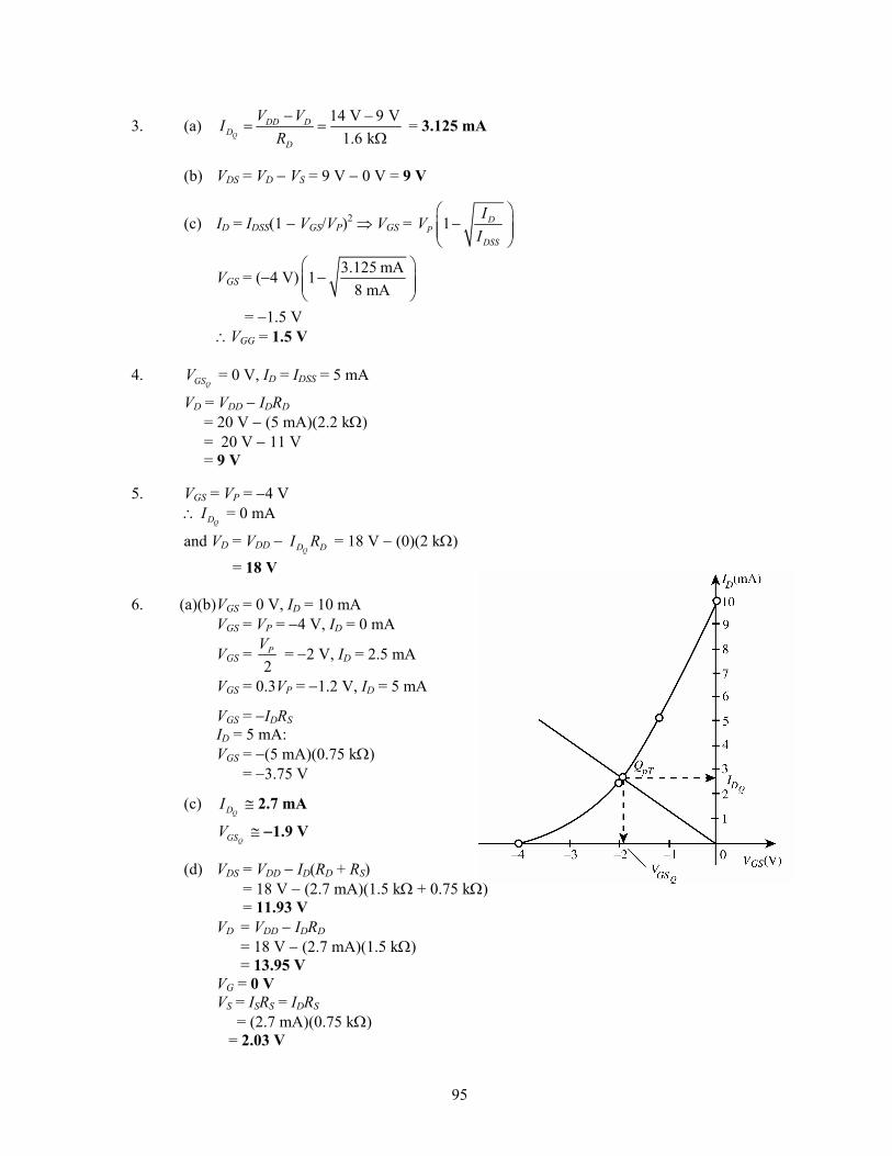
95
3. (a) 14 V 9 V1.6 kQ
DD DD
D
V VIR− −
= =Ω
= 3.125 mA
(b) VDS = VD − VS = 9 V − 0 V = 9 V
(c) ID = IDSS(1 − VGS/VP)2 ⇒ VGS = 1 DP
DSS
IVI
⎛ ⎞−⎜ ⎟⎜ ⎟
⎝ ⎠
VGS = (−4 V) 3.125 mA18 mA
⎛ ⎞−⎜ ⎟⎜ ⎟
⎝ ⎠
= −1.5 V ∴VGG = 1.5 V 4.
QGSV = 0 V, ID = IDSS = 5 mA
VD = VDD − IDRD = 20 V − (5 mA)(2.2 kΩ) = 20 V − 11 V = 9 V 5. VGS = VP = −4 V ∴
QDI = 0 mA
and VD = VDD − QD DI R = 18 V − (0)(2 kΩ)
= 18 V 6. (a)(b) VGS = 0 V, ID = 10 mA VGS = VP = −4 V, ID = 0 mA
VGS = 2PV = −2 V, ID = 2.5 mA
VGS = 0.3VP = −1.2 V, ID = 5 mA
VGS = −IDRS ID = 5 mA: VGS = −(5 mA)(0.75 kΩ) = −3.75 V
(c) QDI ≅ 2.7 mA
QGSV ≅ −1.9 V
(d) VDS = VDD − ID(RD + RS) = 18 V − (2.7 mA)(1.5 kΩ + 0.75 kΩ) = 11.93 V VD = VDD − IDRD = 18 V − (2.7 mA)(1.5 kΩ) = 13.95 V VG = 0 V VS = ISRS = IDRS = (2.7 mA)(0.75 kΩ) = 2.03 V
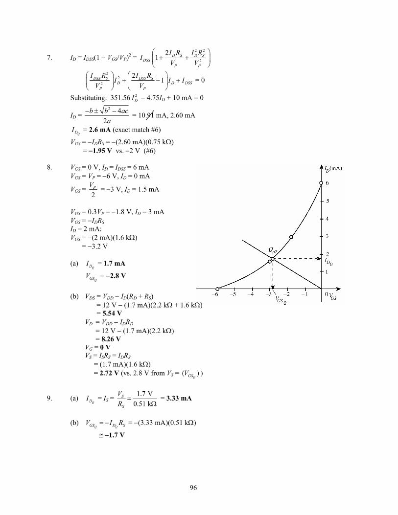
96
7. ID = IDSS(1 − VGS/VP)2 = 2 2
2
21 D S D SDSS
P P
I R I RIV V
⎛ ⎞+ +⎜ ⎟
⎝ ⎠
2
22
2 1DSS S DSS SD D DSS
P P
I R I RI I IV V
⎛ ⎞ ⎛ ⎞+ − +⎜ ⎟ ⎜ ⎟
⎝ ⎠ ⎝ ⎠ = 0
Substituting: 351.56 2DI − 4.75ID + 10 mA = 0
ID = 2 4
2b b ac
a− ± − = 10.91 mA, 2.60 mA
QDI = 2.6 mA (exact match #6)
VGS = −IDRS = −(2.60 mA)(0.75 kΩ) = −1.95 V vs. −2 V (#6) 8. VGS = 0 V, ID = IDSS = 6 mA VGS = VP = −6 V, ID = 0 mA
VGS = 2PV = −3 V, ID = 1.5 mA
VGS = 0.3VP = −1.8 V, ID = 3 mA VGS = −IDRS ID = 2 mA: VGS = −(2 mA)(1.6 kΩ) = −3.2 V (a)
QDI = 1.7 mA
QGSV = −2.8 V
(b) VDS = VDD − ID(RD + RS) = 12 V − (1.7 mA)(2.2 kΩ + 1.6 kΩ) = 5.54 V VD = VDD − IDRD = 12 V − (1.7 mA)(2.2 kΩ) = 8.26 V VG = 0 V VS = ISRS = IDRS = (1.7 mA)(1.6 kΩ) = 2.72 V (vs. 2.8 V from VS = ( )
QGSV )
9. (a) QDI = IS = 1.7 V
0.51 kS
S
VR
=Ω
= 3.33 mA
(b)
Q QGS D SV I R= − = −(3.33 mA)(0.51 kΩ)
≅ −1.7 V
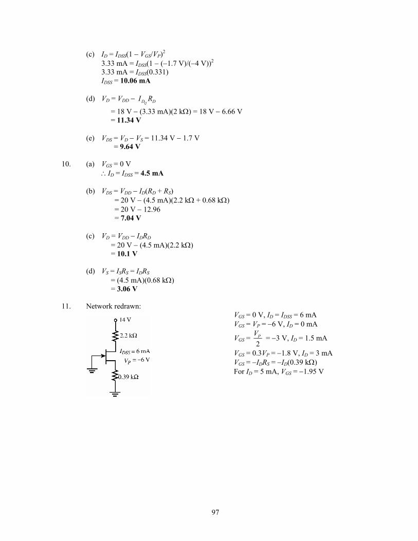
97
(c) ID = IDSS(1 − VGS/VP)2 3.33 mA = IDSS(1 − (−1.7 V)/(−4 V))2 3.33 mA = IDSS(0.331) IDSS = 10.06 mA (d) VD = VDD −
QD DI R
= 18 V − (3.33 mA)(2 kΩ) = 18 V − 6.66 V = 11.34 V (e) VDS = VD − VS = 11.34 V − 1.7 V = 9.64 V 10. (a) VGS = 0 V ∴ID = IDSS = 4.5 mA (b) VDS = VDD − ID(RD + RS) = 20 V − (4.5 mA)(2.2 kΩ + 0.68 kΩ) = 20 V − 12.96 = 7.04 V (c) VD = VDD − IDRD = 20 V − (4.5 mA)(2.2 kΩ) = 10.1 V (d) VS = ISRS = IDRS = (4.5 mA)(0.68 kΩ) = 3.06 V 11. Network redrawn:
VGS = 0 V, ID = IDSS = 6 mA VGS = VP = −6 V, ID = 0 mA
VGS = 2PV = −3 V, ID = 1.5 mA
VGS = 0.3VP = −1.8 V, ID = 3 mA VGS = −IDRS = −ID(0.39 kΩ) For ID = 5 mA, VGS = −1.95 V
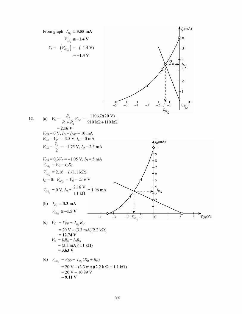
98
From graph QDI ≅ 3.55 mA
QGSV ≅ −1.4 V
VS = ( )QGSV− = −(−1.4 V)
= +1.4 V
12. (a) VG = 2
1 2DD
R VR R+
= 110 k (20 V)910 k 110 k
ΩΩ+ Ω
= 2.16 V VGS = 0 V, ID = IDSS = 10 mA VGS = VP = −3.5 V, ID = 0 mA
VGS = 2PV = −1.75 V, ID = 2.5 mA
VGS = 0.3VP = −1.05 V, ID = 5 mA
QGSV = VG − IDRS
QGSV = 2.16 − ID(1.1 kΩ)
ID = 0: QGSV = VG = 2.16 V
QGSV = 0 V, ID = 2.16 V
1.1 kΩ = 1.96 mA
(b)
QDI ≅ 3.3 mA
QGSV ≅ −1.5 V
(c) VD = VDD −
QD DI R
= 20 V − (3.3 mA)(2.2 kΩ) = 12.74 V VS = ISRS = IDRS = (3.3 mA)(1.1 kΩ) = 3.63 V (d)
QDSV = VDD − ( )QD D SI R R+
= 20 V − (3.3 mA)(2.2 k Ω + 1.1 kΩ) = 20 V − 10.89 V = 9.11 V
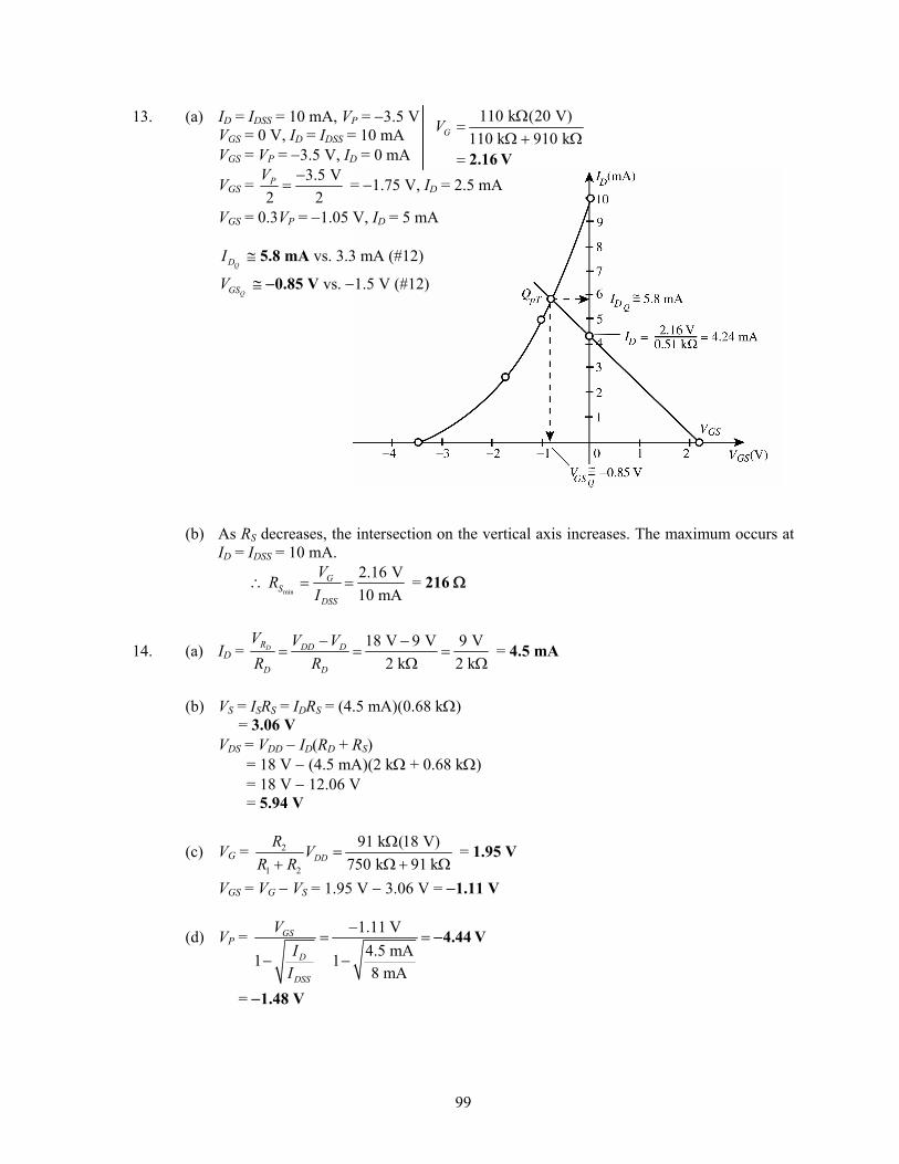
99
110 k (20 V)110 k 910 kGV Ω
=Ω + Ω
= 2.16 V
13. (a) ID = IDSS = 10 mA, VP = −3.5 V VGS = 0 V, ID = IDSS = 10 mA VGS = VP = −3.5 V, ID = 0 mA
VGS = 3.5 V2 2PV −= = −1.75 V, ID = 2.5 mA
VGS = 0.3VP = −1.05 V, ID = 5 mA
QDI ≅ 5.8 mA vs. 3.3 mA (#12)
QGSV ≅ −0.85 V vs. −1.5 V (#12)
(b) As RS decreases, the intersection on the vertical axis increases. The maximum occurs at
ID = IDSS = 10 mA.
∴min
2.16 V10 mA
GS
DSS
VRI
= = = 216 Ω
14. (a) ID = 18 V 9 V 9 V2 k 2 k
DR DD D
D D
V V VR R
− −= = =
Ω Ω = 4.5 mA
(b) VS = ISRS = IDRS = (4.5 mA)(0.68 kΩ) = 3.06 V VDS = VDD − ID(RD + RS) = 18 V − (4.5 mA)(2 kΩ + 0.68 kΩ) = 18 V − 12.06 V = 5.94 V
(c) VG = 2
1 2
91 k (18 V)750 k 91 kDD
R VR R
Ω=
+ Ω + Ω = 1.95 V
VGS = VG − VS = 1.95 V − 3.06 V = −1.11 V
(d) VP = 1.11 V4.5 mA1 18 mA
GS
D
DSS
VI
I
−= =
− −4.44 V−
= −1.48 V
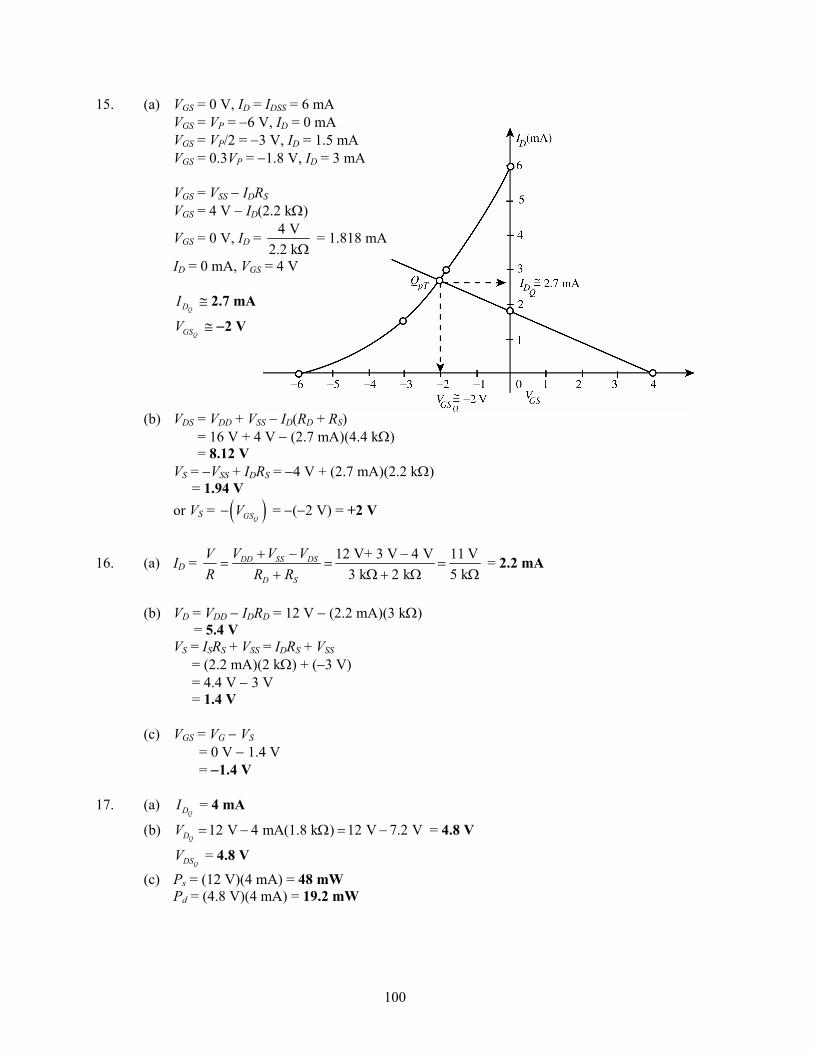
100
15. (a) VGS = 0 V, ID = IDSS = 6 mA VGS = VP = −6 V, ID = 0 mA VGS = VP/2 = −3 V, ID = 1.5 mA VGS = 0.3VP = −1.8 V, ID = 3 mA VGS = VSS − IDRS
VGS = 4 V − ID(2.2 kΩ)
VGS = 0 V, ID = 4 V2.2 kΩ
= 1.818 mA
ID = 0 mA, VGS = 4 V
QDI ≅ 2.7 mA
QGSV ≅ −2 V
(b) VDS = VDD + VSS − ID(RD + RS) = 16 V + 4 V − (2.7 mA)(4.4 kΩ) = 8.12 V VS = −VSS + IDRS = −4 V + (2.7 mA)(2.2 kΩ) = 1.94 V or VS = ( )QGSV− = −(−2 V) = +2 V
16. (a) ID = 12 V+ 3 V 4 V 11 V3 k 2 k 5 k
DD SS DS
D S
V V VVR R R
+ − −= = =
+ Ω + Ω Ω = 2.2 mA
(b) VD = VDD − IDRD = 12 V − (2.2 mA)(3 kΩ) = 5.4 V VS = ISRS + VSS = IDRS + VSS = (2.2 mA)(2 kΩ) + (−3 V) = 4.4 V − 3 V = 1.4 V (c) VGS = VG − VS = 0 V − 1.4 V = −1.4 V 17. (a)
QDI = 4 mA
(b) 12 V 4 mA(1.8 k ) 12 V 7.2 VQDV = − Ω = − = 4.8 V
QDSV = 4.8 V
(c) Ps = (12 V)(4 mA) = 48 mW Pd = (4.8 V)(4 mA) = 19.2 mW
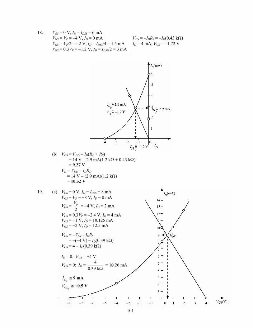
101
18. VGS = 0 V, ID = IDSS = 6 mA VGS = VP = −4 V, ID = 0 mA VGS = VP/2 = −2 V, ID = IDSS/4 = 1.5 mA VGS = 0.3VP = −1.2 V, ID = IDSS/2 = 3 mA
VGS = −IDRS = −ID(0.43 kΩ) ID = 4 mA, VGS = −1.72 V
(b) VDS = VDD − ID(RD + RS) = 14 V − 2.9 mA(1.2 kΩ + 0.43 kΩ) = 9.27 V VD = VDD − IDRD = 14 V − (2.9 mA)(1.2 kΩ) = 10.52 V 19. (a) VGS = 0 V, ID = IDSS = 8 mA VGS = VP = −8 V, ID = 0 mA
VGS = 2PV = −4 V, ID = 2 mA
VGS = 0.3VP = −2.4 V, ID = 4 mA VGS = +1 V, ID = 10.125 mA VGS = +2 V, ID = 12.5 mA VGS = −VSS − IDRS = −(−4 V) − ID(0.39 kΩ) VGS = 4 − ID(0.39 kΩ) ID = 0: VGS = +4 V
VGS = 0: ID = 40.39 kΩ
= 10.26 mA
QDI ≅ 9 mA
QGSV ≅ +0.5 V
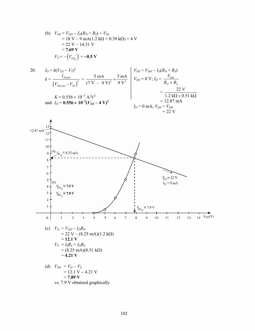
102
(b) VDS = VDD − ID(RD + RS) + VSS = 18 V − 9 mA(1.2 kΩ + 0.39 kΩ) + 4 V = 22 V − 14.31 V = 7.69 V VS = ( )QGSV− = −0.5 V
20. ID = k(VGS − VT)2
k = ( )
(on)2
(on)
D
GS Th
I
V V− = 2 2
5 mA 5 mA(7 V 4 V) 9 V
=−
K = 0.556 × 10⁻³ A/V2 and ID = 0.556 × 10⁻³(VGS − 4 V)2
VDS = VDD − ID(RD + RS)
VDS = 0 V; ID = DD
D S
VR R+
= 22 V1.2 k 0.51 kΩ+ Ω
= 12.87 mA ID = 0 mA, VDS = VDD = 22 V
(c) VD = VDD − IDRD = 22 V − (8.25 mA)(1.2 kΩ) = 12.1 V VS = ISRS = IDRS = (8.25 mA)(0.51 kΩ) = 4.21 V (d) VDS = VD − VS = 12.1 V − 4.21 V = 7.89 V vs. 7.9 V obtained graphically
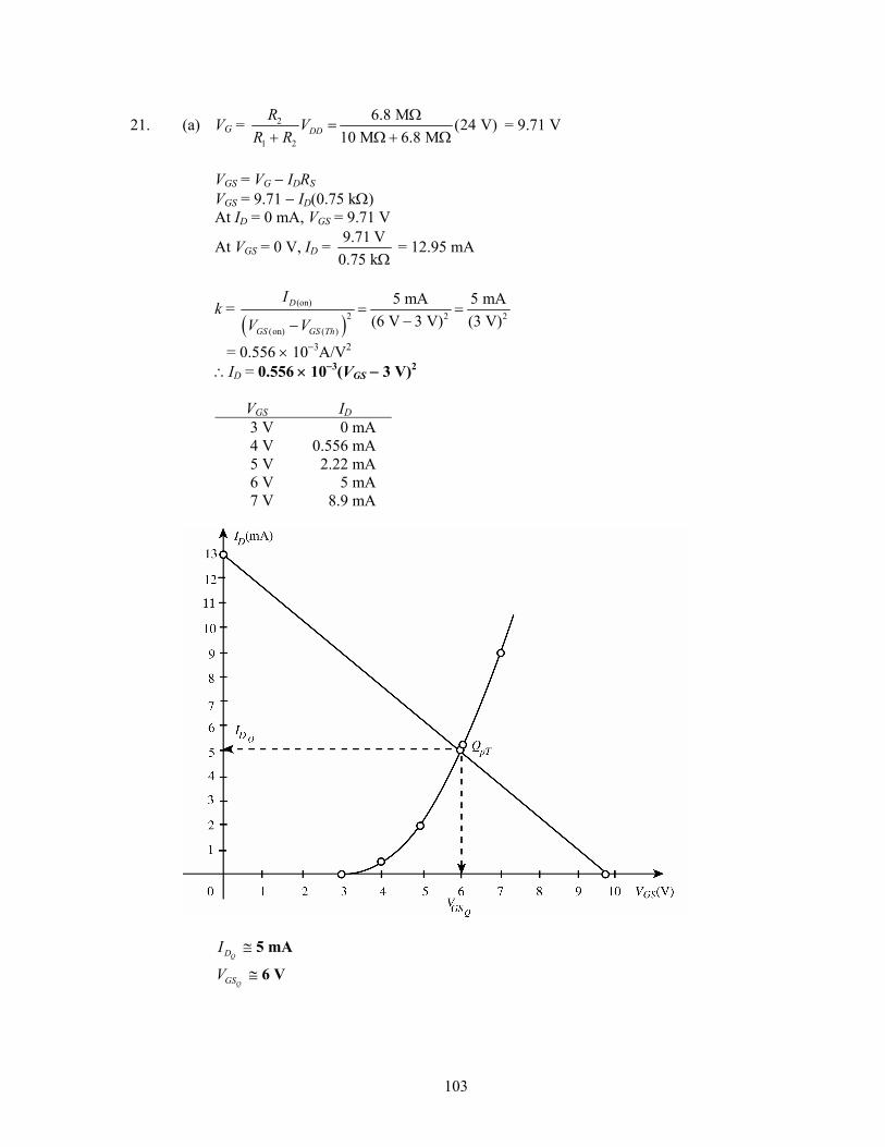
103
21. (a) VG = 2
1 2
6.8 M (24 V)10 M 6.8 MDD
R VR R
Ω=
+ Ω + Ω = 9.71 V
VGS = VG − IDRS VGS = 9.71 − ID(0.75 kΩ) At ID = 0 mA, VGS = 9.71 V
At VGS = 0 V, ID = 9.71 V0.75 kΩ
= 12.95 mA
k = ( )
(on)2 2 2
(on) ( )
5 mA 5 mA(6 V 3 V) (3 V)
D
GS GS Th
I
V V= =
−−
= 0.556 × 10⁻³A/V2 ∴ID = 0.556 × 10⁻³(VGS − 3 V)2
VGS ID 3 V 0 mA 4 V 0.556 mA 5 V 2.22 mA 6 V 5 mA 7 V 8.9 mA
QDI ≅ 5 mA
QGSV ≅ 6 V
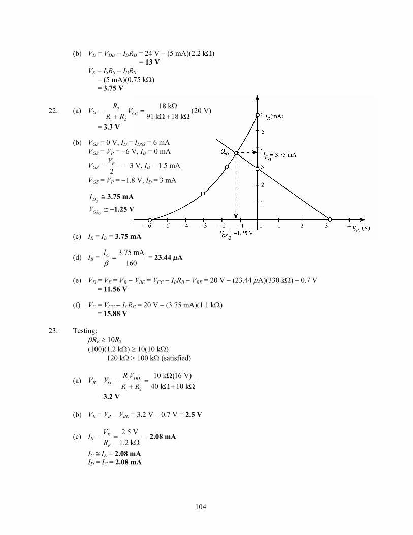
104
(b) VD = VDD − IDRD = 24 V − (5 mA)(2.2 kΩ) = 13 V VS = ISRS = IDRS = (5 mA)(0.75 kΩ) = 3.75 V
22. (a) VG = 2
1 2
18 k (20 V)91 k 18 kCC
R VR R
Ω=
+ Ω + Ω
= 3.3 V (b) VGS = 0 V, ID = IDSS = 6 mA VGS = VP = −6 V, ID = 0 mA
VGS = 2PV = −3 V, ID = 1.5 mA
VGS = VP = −1.8 V, ID = 3 mA
QDI ≅ 3.75 mA
QGSV ≅ −1.25 V
(c) IE = ID = 3.75 mA
(d) IB = 3.75 mA160
CIβ
= = 23.44 μA
(e) VD = VE = VB − VBE = VCC − IBRB − VBE = 20 V − (23.44 μA)(330 kΩ) − 0.7 V = 11.56 V (f) VC = VCC − ICRC = 20 V − (3.75 mA)(1.1 kΩ) = 15.88 V 23. Testing: βRE ≥ 10R2 (100)(1.2 kΩ) ≥ 10(10 kΩ) 120 kΩ > 100 kΩ (satisfied)
(a) VB = VG = 2
1 2
10 k (16 V)40 k 10 k
DDR VR R
Ω=
+ Ω + Ω
= 3.2 V (b) VE = VB − VBE = 3.2 V − 0.7 V = 2.5 V
(c) IE = 2.5 V1.2 k
E
E
VR
=Ω
= 2.08 mA
IC ≅ IE = 2.08 mA ID = IC = 2.08 mA
105
(d) IB = 2.08 mA100
CIβ
= = 20.8 μA
(e) VC = VG − VGS
VGS = 1 DP
DSS
IVI
⎛ ⎞−⎜ ⎟⎜ ⎟
⎝ ⎠
= 2.08 mA( 6 V) 16 mA
⎛ ⎞− −⎜ ⎟⎜ ⎟
⎝ ⎠
= −2.47 V VC = 3.2 − (−2.47 V) = 5.67 V VS = VC = 5.67 V VD = VDD − IDRD = 16 V − (2.08 mA)(2.2 kΩ) = 11.42 V (f) VCE = VC − VE = 5.67 V − 2.5 V = 3.17 V (g) VDS = VD − VS = 11.42 V − 5.67 V = 5.75 V
24. VGS = 1 DP
DSS
IVI
⎛ ⎞−⎜ ⎟⎜ ⎟
⎝ ⎠ = (−6 V) 4 mA1
8 mA⎛ ⎞−⎜ ⎟⎜ ⎟
⎝ ⎠
= −1.75 V
VGS = −IDRS: RS = ( 1.75 V)4 mA
GS
D
VI
− −− = = 0.44 kΩ
RD = 3RS = 3(0.44 kΩ) = 1.32 kΩ Standard values: RS = 0.43 kΩ RD = 1.3 kΩ
25. VGS = 1 DP
DSS
IVI
⎛ ⎞−⎜ ⎟⎜ ⎟
⎝ ⎠ = (−4 V) 2.5 mA1
10 mA⎛ ⎞−⎜ ⎟⎜ ⎟
⎝ ⎠
= −2 V VGS = VG − VS and VS = VG − VGS = 4 V − (−2 V) = 6 V
RS = 6 V2.5 mA
S
D
VI
= = 2.4 kΩ (a standard value)
RD = 2.5RS = 2.5(2.4 kΩ) = 6 kΩ ⇒ use 6.2 kΩ
VG = 2
1 2
DDR VR R+
⇒ 4 V = 2
2
(24 V)22 M
RRΩ+
⇒ 88 MΩ + 4R2 = 24R2
20R2 = 88 MΩ R2 = 4.4 MΩ Use R2 = 4.3 MΩ
106
26. ID = k(VGS − VT)2
DIk
= (VGS − VT)2
DIk
= VGS − VT
and VGS = VT + DIk
= 4 V + 3 2
6 mA0.5 10 A/V−×
= 7.46 V
RD = 16 V 7.46 V 8.54 V6 mA 6 mA
DR DD DS DD GS
D D D
V V V V VI I I
− − −= = = =
= 1.42 kΩ Standard value: RD = 0.75 kΩ RG = 10 MΩ
27. (a) ID = IS = 4 V1 k
S
S
VR
=Ω
= 4 mA
VDS = VDD − ID(RD + RS) = 12 V − (4 mA)(2 kΩ + 1 kΩ) = 12 V − (4 mA)(3 kΩ) = 12 V − 12 V = 0 V JFET in saturation! (b) VS = 0 V reveals that the JFET is nonconducting and the JFET is either defective or an
open-circuit exists in the output circuit. VS is at the same potential as the grounded side of the 1 kΩ resistor.
(c) Typically, the voltage across the 1 MΩ resistor is ≅ 0 V. The fact that the voltage across
the 1 MΩ resistor is equal to VDD suggests that there is a short-circuit connection from gate to drain with ID = 0 mA. Either the JFET is defective or an improper circuit connection was made.
28. VG = 75 k (20 V)75 k 330 k
ΩΩ+ Ω
= 3.7 V (seems correct!)
VGS = 3.7 V − 6.25 V = −2.55 V (possibly okay) ID = IDSS(1 − VGS/VP)2 = 10 mA(1 − (−2.55 V)/(−6 V))2 = 3.3 mA (reasonable)
However, IS = 6.25 V1 k
S
S
VR
=Ω
= 6.25 mA ≠ 3.3 mA
DRV = IDRD = ISRD = (6.25 mA)(2.2 kΩ)
= 13.75 V and
S DR RV V+ = 6.25 V + 13.75 V = 20 V = VDD ∴VDS = 0 V 1. Possible short-circuit from D-S. 2. Actual IDSS and/or VP may be larger in magnitude than specified.
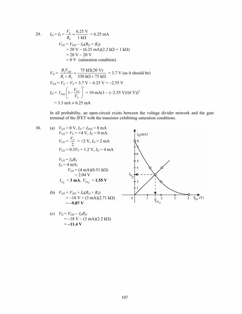
107
29. ID = IS = 6.25 V1 k
S
S
VR
=Ω
= 6.25 mA
VDS = VDD − ID(RD + RS) = 20 V − (6.25 mA)(2.2 kΩ + 1 kΩ) = 20 V − 20 V = 0 V (saturation condition)
VG = 2
1 2
75 k (20 V)330 k 75 k
DDR VR R
Ω=
+ Ω + Ω = 3.7 V (as it should be)
VGS = VG − VS = 3.7 V − 6.25 V = −2.55 V
ID = 2
1 GSDSS
P
VIV
⎛ ⎞−⎜ ⎟
⎝ ⎠ = 10 mA(1 − (−2.55 V)/(6 V))2
= 3.3 mA ≠ 6.25 mA In all probability, an open-circuit exists between the voltage divider network and the gate
terminal of the JFET with the transistor exhibiting saturation conditions. 30. (a) VGS = 0 V, ID = IDSS = 8 mA VGS = VP = +4 V, ID = 0 mA
VGS = 2PV = +2 V, ID = 2 mA
VGS = 0.3VP = 1.2 V, ID = 4 mA VGS = IDRS ID = 4 mA; VGS = (4 mA)(0.51 kΩ) = 2.04 V
QDI = 3 mA, QGSV = 1.55 V
(b) VDS = VDD + ID(RD + RS) = −18 V + (3 mA)(2.71 kΩ) = −9.87 V (c) VD = VDD − IDRD = −18 V − (3 mA)(2.2 kΩ) = −11.4 V
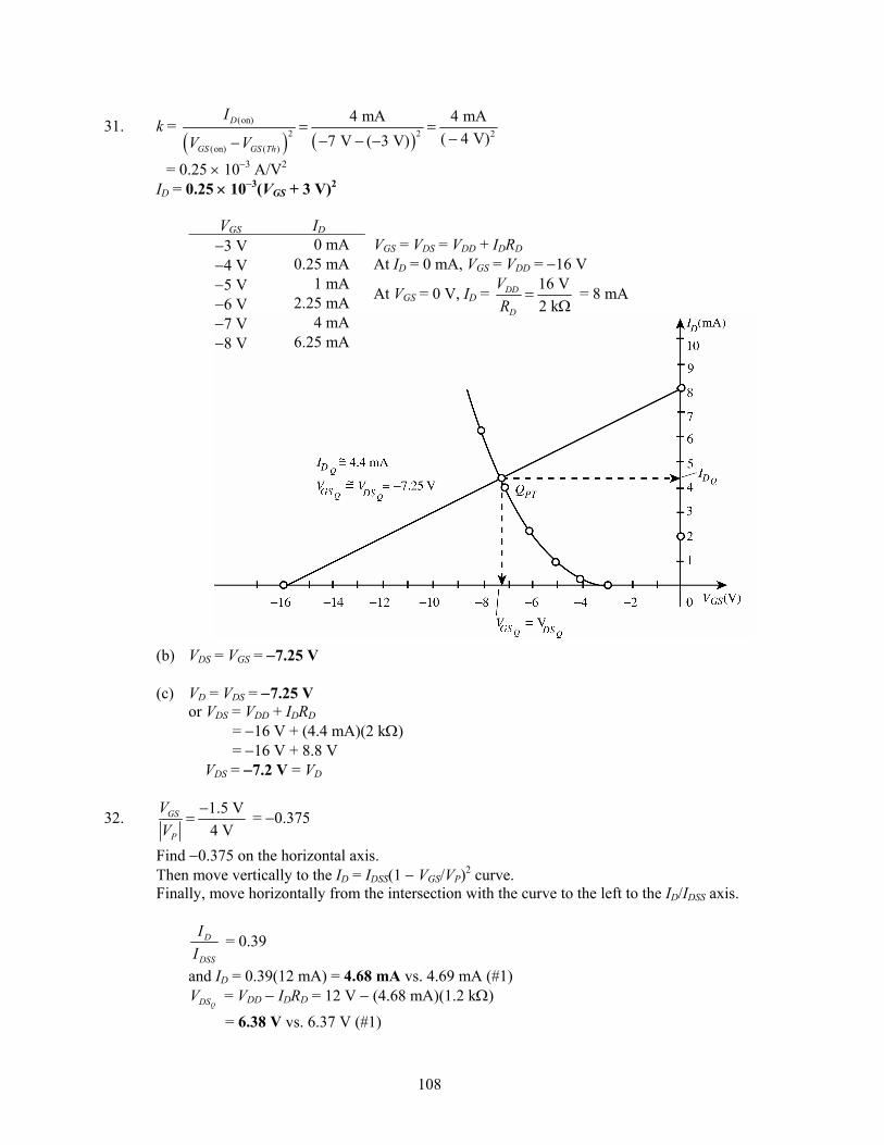
108
31. k = ( ) ( )
(on)2 2 2
(on) ( )
4 mA 4 mA( 4 V)7 V ( 3 V)
D
GS GS Th
I
V V= =
−− − −−
= 0.25 × 10⁻³ A/V2 ID = 0.25 × 10⁻³(VGS + 3 V)2
VGS ID −3 V 0 mA −4 V 0.25 mA −5 V 1 mA −6 V 2.25 mA −7 V 4 mA −8 V 6.25 mA
VGS = VDS = VDD + IDRD At ID = 0 mA, VGS = VDD = −16 V
At VGS = 0 V, ID = 16 V2 k
DD
D
VR
=Ω
= 8 mA
(b) VDS = VGS = −7.25 V (c) VD = VDS = −7.25 V or VDS = VDD + IDRD = −16 V + (4.4 mA)(2 kΩ) = −16 V + 8.8 V VDS = −7.2 V = VD
32. 1.5 V4 V
GS
P
VV
−= = −0.375
Find −0.375 on the horizontal axis. Then move vertically to the ID = IDSS(1 − VGS/VP)2 curve. Finally, move horizontally from the intersection with the curve to the left to the ID/IDSS axis.
D
DSS
II
= 0.39
and ID = 0.39(12 mA) = 4.68 mA vs. 4.69 mA (#1)
QDSV = VDD − IDRD = 12 V − (4.68 mA)(1.2 kΩ)
= 6.38 V vs. 6.37 V (#1)
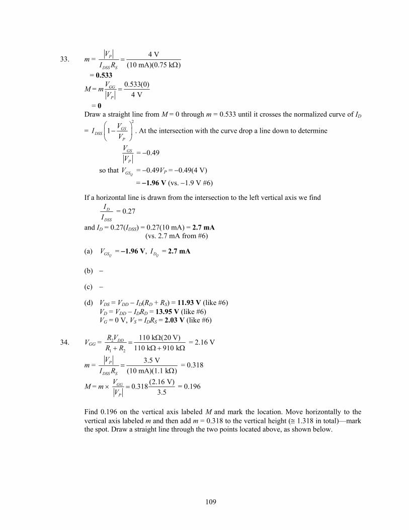
109
33. m = 4 V(10 mA)(0.75 k )
P
DSS S
VI R
=Ω
= 0.533
M = m 0.533(0)4 V
GG
P
VV
=
= 0 Draw a straight line from M = 0 through m = 0.533 until it crosses the normalized curve of ID
= 2
1 GSDSS
P
VIV
⎛ ⎞−⎜ ⎟
⎝ ⎠. At the intersection with the curve drop a line down to determine
GS
P
VV
= −0.49
so that QGSV = −0.49VP = −0.49(4 V)
= −1.96 V (vs. −1.9 V #6) If a horizontal line is drawn from the intersection to the left vertical axis we find
D
DSS
II
= 0.27
and ID = 0.27(IDSS) = 0.27(10 mA) = 2.7 mA (vs. 2.7 mA from #6) (a)
QGSV = −1.96 V, QDI = 2.7 mA
(b) − (c) − (d) VDS = VDD − ID(RD + RS) = 11.93 V (like #6) VD = VDD − IDRD = 13.95 V (like #6) VG = 0 V, VS = IDRS = 2.03 V (like #6)
34. VGG = 2
1 2
110 k (20 V)110 k 910 k
DDR VR R
Ω=
+ Ω + Ω = 2.16 V
m = 3.5 V(10 mA)(1.1 k )
P
DSS S
VI R
=Ω
= 0.318
M = m × (2.16 V)0.3183.5
GG
P
VV
= = 0.196
Find 0.196 on the vertical axis labeled M and mark the location. Move horizontally to the
vertical axis labeled m and then add m = 0.318 to the vertical height (≅ 1.318 in total)—mark the spot. Draw a straight line through the two points located above, as shown below.
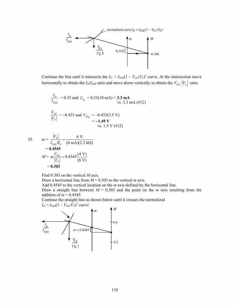
110
Continue the line until it intersects the ID = IDSS(1 − VGS/VP)2 curve. At the intersection move
horizontally to obtain the ID/IDSS ratio and move down vertically to obtain the /GS pV V ratio.
D
DSS
II
= 0.33 and QDI = 0.33(10 mA) = 3.3 mA
GS
P
VV
= −0.425 and QGSV = −0.425(3.5 V)
vs. 1.5 V (#12)
35. m = 6 V(6 mA)(2.2 k )
P
DSS S
VI R
=Ω
= 0.4545
M = (4 V)0.4545(6 V)
GG
P
VmV
=
= 0.303 Find 0.303 on the vertical M axis. Draw a horizontal line from M = 0.303 to the vertical m axis. Add 0.4545 to the vertical location on the m axis defined by the horizontal line. Draw a straight line between M = 0.303 and the point on the m axis resulting from the
addition of m = 0.4545. Continue the straight line as shown below until it crosses the normalized ID = IDSS(1 − VGS/VP)2 curve:
vs. 3.3 mA (#12)
= −1.49 V
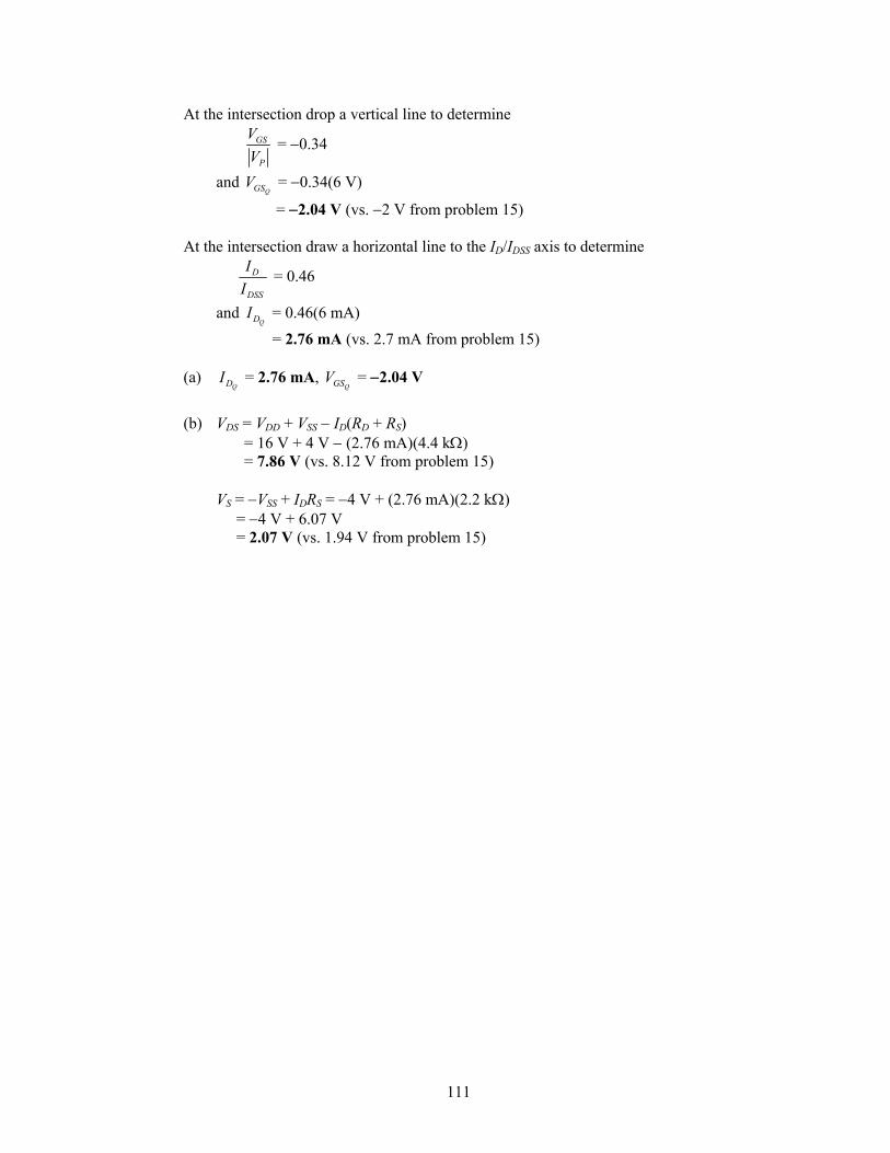
111
At the intersection drop a vertical line to determine
GS
P
VV
= −0.34
and QGSV = −0.34(6 V)
= −2.04 V (vs. −2 V from problem 15) At the intersection draw a horizontal line to the ID/IDSS axis to determine
D
DSS
II
= 0.46
and QDI = 0.46(6 mA)
= 2.76 mA (vs. 2.7 mA from problem 15) (a)
QDI = 2.76 mA, QGSV = −2.04 V
(b) VDS = VDD + VSS − ID(RD + RS) = 16 V + 4 V − (2.76 mA)(4.4 kΩ) = 7.86 V (vs. 8.12 V from problem 15) VS = −VSS + IDRS = −4 V + (2.76 mA)(2.2 kΩ) = −4 V + 6.07 V = 2.07 V (vs. 1.94 V from problem 15)
112
Chapter 8
1. gm0 = 2 2(15 mA)5 V
DSS
P
IV
=−
= 6 mS
2. gm0 = 0
2 2 2(12 mA)10 mS
DSS DSSP
P m
I IVV g
⇒ = = = 2.4 V
VP = −2.4 V
3. gm0 = 2 DSS
P
IV
⇒ IDSS = ( )( ) 5 mS(3.5 V)
2 2mO Pg V
= = 8.75 mA
4. gm = 02(12 mA) 1 V1 1
3 V 3 VQGS
mP
Vg
V⎛ ⎞ −⎛ ⎞− = −⎜ ⎟ ⎜ ⎟⎜ ⎟ − −⎝ ⎠⎝ ⎠
= 5.3 mS
5. gm = 2 1 QGSDSS
P P
VIV V
⎛ ⎞−⎜ ⎟⎜ ⎟
⎝ ⎠
6 mS = 2 1 V12.5 V 2.5 V
DSSI −⎛ ⎞−⎜ ⎟−⎝ ⎠
IDSS = 12.5 mA
6. gm = 02 / 4 2(10 mA) 1
5 V 4DSS DSSD
mDSS P DSS
I IIgI V I
= =
= 20 mA 15 V 2
⎛ ⎞⎜ ⎟⎝ ⎠
= 2 mS
7. gm0 = 2 2(8 mA)5 V
DSS
P
IV
= = 3.2 mS
gm = 0/ 41 3.2 mS 1QGS P
mP P
V VgV V
⎛ ⎞ ⎛ ⎞− = −⎜ ⎟ ⎜ ⎟⎜ ⎟ ⎝ ⎠⎝ ⎠
= 3.2 mS 1 31 3.2 mS4 4
⎛ ⎞ ⎛ ⎞− =⎜ ⎟ ⎜ ⎟⎝ ⎠ ⎝ ⎠
= 2.4 mS 8. (a) gm = yfs = 4.5 mS
(b) rd = 1 125 Sosy μ
= = 40 kΩ
9. gm = yfs = 4.5 mS
rd = 1 125 Sosy μ
= = 40 kΩ
Zo = rd = 40 kΩ Av(FET) = −gmrd = −(4.5 mS)(40 kΩ) = −180
113
10. Av = −gmrd ⇒ gm = ( 200)(100 k )
v
d
Ar− −
= −Ω
= 2 mS
11. (a) gm0 = 2 2(10 mA)5 V
DSS
P
IV
= = 4 mS
(b) gm = 6.4 mA 3.6 mA2 V 1 V
D
GS
IVΔ −
=Δ −
= 2.8 mS
(c) Eq. 8.6: gm = 01.5 V1 4 mS 15 V
QGSm
P
Vg
V⎛ ⎞ −⎛ ⎞− = −⎜ ⎟ ⎜ ⎟⎜ ⎟ −⎝ ⎠⎝ ⎠
= 2.8 mS
(d) gm = 3.6 mA 1.6 mA3 V 2 V
D
GS
IVΔ −
=Δ −
= 2 mS
(e) gm = 02.5 V1 4 mS 15 V
QGSm
P
Vg
V⎛ ⎞ −⎛ ⎞− = −⎜ ⎟ ⎜ ⎟⎜ ⎟ −⎝ ⎠⎝ ⎠
= 2 mS
12. (a) rd = constant
(15 V 5 V) 10 V(9.1 mA 8.8 mA) 0.3 mA
GS
DS
D V
VI
Δ −= =
Δ − = 33.33 kΩ
(b) At VDS = 10 V, ID = 9 mA on VGS = 0 V curve
∴gm0 = 2 2(9 mA)4 V
DSS
P
IV
= = 4.5 mS
13. From 2N4220 data: gm = yfs = 750 μS = 0.75 mS
rd = 1 110 Sosy μ
= = 100 kΩ
14. (a) gm (@ VGS = −6 V) = 0, gm (@ VGS = 0 V) = gm0 = 2 2(8 mA)6 V
DSS
P
IV
= = 2.67 mS
(b) gm (@ ID = 0 mA) = 0, gm (@ ID = IDSS = 8 mA) = gm0 = 2.67 mS
15. gm = yfs = 5.6 mS, rd = 1 115 Sosy μ
= = 66.67 kΩ
16. gm = 2 2(10 mA) 2 V1 14 V 4 V
QGSDSS
P P
VIV V
⎛ ⎞ −⎛ ⎞− = −⎜ ⎟ ⎜ ⎟⎜ ⎟ −⎝ ⎠⎝ ⎠ = 2.5 mS
rd = 1 125 Sosy μ
= = 40 kΩ
114
17. Graphically, QGSV = −1.5 V
gm = 2 2(10 mA) 1.5 V1 14 V 4 V
QGSDSS
P P
VIV V
⎛ ⎞ −⎛ ⎞− = −⎜ ⎟ ⎜ ⎟⎜ ⎟ −⎝ ⎠⎝ ⎠ = 3.125 mS
Zi = RG = 1 MΩ Zo = RD || rd = 1.8 kΩ || 40 kΩ = 1.72 kΩ Av = −gm(RD || rd) = −(3.125 mS)(1.72 kΩ) = −5.375 18.
QGSV = −1.5 V
gm = 2 2(12 mA) 1.5 V1 16 V 6 V
QGSDSS
P P
VIV V
⎛ ⎞ −⎛ ⎞− = −⎜ ⎟ ⎜ ⎟⎜ ⎟ −⎝ ⎠⎝ ⎠ = 3 mS
Zi = RG = 1 MΩ
Zo = RD || rd, rd = 1 140 Sosy μ
= = 25 kΩ
= 1.8 kΩ || 25 kΩ = 1.68 kΩ Av = −gm(RD || rd) = −(3 mS)(1.68 kΩ) = −5.04 19. gm = yfs = 3000 μS = 3 mS
rd = 1 150 Sosy μ
= = 20 kΩ
Zi = RG = 10 MΩ Zo = rd || RD = 20 kΩ|| 3.3 kΩ = 2.83 kΩ Av = −gm(rd || RD) = −(3 mS)(2.83 kΩ) = −8.49
20. QGSV = 0 V, gm = gm0 = 2 2(6 mA)
6 VDSS
P
IV
= = 2 mS, rd = 1 140 Sosy μ
= = 25 kΩ
Zi = 1 MΩ Zo = rd || RD = 25 kΩ || 2 kΩ = 1.852 kΩ Av = −gm(rd || RD) = −(2 mS)(1.852 kΩ) ≅ −3.7
115
21. gm = 3 mS, rd = 20 kΩ Zi = 10 MΩ
Zo = 3.3 k3.3 k 1.1 k1 (3 mS)(1.1 k )1
20 k
D
D Sm S
d
RR Rg R
r
Ω=
+ Ω + Ω+ Ω ++ +
Ω
= 3.3 k 3.3 k1 3.3 0.22 4.52
Ω Ω=
+ + = 730 Ω
Av = (3 mS)(3.3 k )3.3 k 1.1 k1 (3 mS)(1.1 k )1
20 k
m D
D Sm S
d
g RR Rg R
r
− − Ω=
+ Ω + Ω+ Ω ++ +
Ω
= 9.9 9.91 3.3 0.22 4.52
−= −
+ + = −2.19
22. gm = yfs = 3000 μS = 3 mS
rd = 1 110 Sosy μ
= = 100 kΩ
Zi = RG = 10 MΩ (the same) Zo = rd || RD = 100 kΩ || 3.3 kΩ = 3.195 kΩ (higher) Av = −gm(rd || RD) = −(3 mS)(3.195 kΩ) = −9.59 (higher) 23.
QGSV = −0.95 V
gm = 2 1 QGSDSS
P P
VIV V
⎛ ⎞−⎜ ⎟⎜ ⎟
⎝ ⎠
= 2(12 mA) 0.95 V13 V 3 V
−⎛ ⎞−⎜ ⎟−⎝ ⎠
= 5.47 mS Zi = 82 MΩ || 11 MΩ = 9.7 MΩ Zo = rd || RD = 100 kΩ || 2 kΩ = 1.96 kΩ Av = −gm(rd || RD) = −(5.47 mS)(1.96 kΩ) = −10.72 Vo = AvVi = (−10.72)(20 mV) = −214.4 mV 24.
QGSV = −0.95 V (as before), gm = 5.47 mS (as before)
Zi = 9.7 MΩ as before
Zo = 1
D
D Sm S
d
RR Rg R
r+
+ +
but rd ≥ 10(RD + RS)
116
∴Zo = 2 k 2 k 2 k1 1 (5.47 mS)(0.61 k ) 1 3.337 4.337
D
m S
Rg R
Ω Ω Ω= = =
+ + Ω +
= 461.1 Ω
Av = 1
m D
m S
g Rg R
−+
since rd ≥ 10(RD + RS)
= (5.47 mS)(2 k ) 10.944.337 (from above) 4.337− Ω
= − = −2.52 (a big reduction)
Vo = AvVi = (−2.52)(20 mV) = −50.40 mV (compared to −214.4 mV earlier) 25.
QGSV = −0.95 V, gm (problem 23) = 5.47 mS
Zi (the same) = 9.7 MΩ Zo (reduced) = rd || RD = 20 kΩ || 2 kΩ = 1.82 kΩ Av (reduced) = −gm(rd || RD) = −(5.47 mS)(1.82 kΩ) = −9.94 Vo (reduced) = AvVi = (−9.94)(20 mV) = −198.8 mV 26.
QGSV = −0.95 V (as before), gm = 5.47 mS (as before)
Zi = 9.7 MΩ as before
Zo = 1
D
D Sm S
d
RR Rg R
r+
+ + since rd < 10(RD + RS)
= 2 k2 k 0.61 k1 (5.47 mS)(0.61 k )
20 k
ΩΩ+ Ω
+ Ω +Ω
= 2 k 2 k1 3.33 0.13 4.46
Ω Ω=
+ +
= 448.4 Ω (slightly less than 461.1 Ω obtained in problem 24)
Av = 1
m D
D Sm S
d
g RR Rg R
r
−+
+ +
= (5.47 mS)(2 k )2 k 0.61 k1 (5.47 mS)(0.61 k )
20 k
− ΩΩ+ Ω
+ Ω +Ω
= 10.94 10.941 3.33 0.13 4.46
− −=
+ + = −2.45 slightly less than −2.52 obtained in problem 24)
27. QGSV = −2.85 V, gm = 2 2(9 mA) 2.85 V1 1
4.5 V 4.5 VQGSDSS
P P
VIV V
⎛ ⎞ −⎛ ⎞− = −⎜ ⎟ ⎜ ⎟⎜ ⎟ −⎝ ⎠⎝ ⎠ = 1.47 mS
Zi = RG = 10 MΩ Zo = rd || RS || 1/gm = 40 kΩ || 2.2 kΩ || 1/1.47 mS = 512.9 Ω
680.27 Ω
Av = ( ) (1.47 mS)(40 k 2.2 k ) 3.065
1 ( ) 1 (1.47 mS)(40 k 2.2 k ) 1 3.065m d S
m d S
g r Rg r R
Ω Ω= =
+ + Ω Ω +
= 0.754
117
28. QGSV = −2.85 V, gm = 1.47 mS
Zi = 10 MΩ (as in problem 27) Zo = dr || RS || 1/gm = 20 kΩ || 2.2 kΩ || 680.27 Ω = 506.4 Ω < 512.9 Ω (#27)
1.982 kΩ
Av = ( ) 1.47 mS(20 k 2.2 k ) 2.914
1 ( ) 1 1.47 mS(20 k 2.2 k ) 1 2.914m d S
m d S
g r Rg r R
Ω Ω= =
+ + Ω Ω +
= 0.745 < 0.754 (#27) 29.
QGSV = −3.8 V
gm = 2 2(6 mA) 3.8 V1 16 V 6 V
QGSDSS
P P
VIV V
⎛ ⎞ −⎛ ⎞− = −⎜ ⎟ ⎜ ⎟⎜ ⎟ −⎝ ⎠⎝ ⎠ = 0.733 mS
The network now has the format examined in the text and Zi = RG = 10 MΩ dr′ = rd + RD = 30 kΩ + 3.3 kΩ = 33.3 kΩ
Zo = dr′ || RS || 1/ mg′ = (0.733 mS)(30 k ) 21.99 30 k 3.3 k 33.3 k
m dm
d D
g rgr R
Ω′ = = =+ Ω + Ω Ω
= 0.66 mS
= 33.3 kΩ || 3.3 kΩ || 1/0.66 mS = 3 kΩ || 1.52 kΩ ≅ 1 kΩ
Av = ( ) 0.66 mS(3 k ) 1.98 1.98
1 ( ) 1 0.66 mS(3 k ) 1 1.98 2.98m d S
m d S
g r Rg r R′ ′ Ω
= = =′ ′+ + Ω +
= 0.66 30.
QGSV = −1.75 V, gm = 2.14 mS
rd ≥ 10RD, ∴Zi ≅ RS || 1/gm = 1.5 kΩ || 1/2.14 mS = 1.5 kΩ || 467.29 Ω = 356.3 Ω rd ≥ 10RD, ∴Zo ≅ RD = 3.3 kΩ rd ≥ 10RD, ∴ Av ≅ gmRD = (2.14 mS)(3.3 kΩ) = 7.06 Vo = AvVi = (7.06)(0.1 mV) = 0.706 mV
118
31. QGSV = −1.75 V, gm = 2 2(8 mA) 1.75 V1 1
2.8 V 2.8 VQGSDSS
P P
VIV V
⎛ ⎞ −⎛ ⎞− = −⎜ ⎟ ⎜ ⎟⎜ ⎟ −⎝ ⎠⎝ ⎠ = 2.14 mS
Zi = RS || 25 k 3.3 k 28.3 k1.5 k 1.5 k
1 1 (2.14 mS)(25 k ) 54.5d D
m d
r Rg r
⎡ ⎤ ⎡ ⎤+ Ω + Ω Ω= Ω = Ω⎢ ⎥ ⎢ ⎥+ + Ω⎣ ⎦⎣ ⎦
= 1.5 kΩ || 0.52 kΩ = 386.1 Ω Zo = RD || rd = 3.3 kΩ || 25 kΩ = 2.92 kΩ
Av = / (2.14 mS)(3.3 k ) 3.3 k / 25 k1 / 1 3.3 k / 25 k
m D D d
D d
g R R rR r+ Ω + Ω Ω
=+ + Ω Ω
= 7.062 0.132 7.1941 0.132 1.132
+=
+ = 6.36
Vo = AvVi = (6.36)(0.1 mV) = 0.636 mV 32.
QGSV ≅ −1.2 V, gm = 2.63 mS
rd ≥ 10RD, ∴ Zi ≅ RS || 1/gm = 1 kΩ || 1/2.63 mS = 1 kΩ || 380.2 Ω = 275.5 Ω Zo ≅ RD = 2.2 kΩ Av ≅ gmRD = (2.63 mS)(2.2 kΩ) = 5.79
33. rd = 1 120 Sosy μ
= = 50 kΩ, QGSV = 0 V
gm = gm0 = 2 2(8 mA)3
DSS
P
IV
= = 5.33 mS
Av = −gmRD = −(5.33 mS)(1.1 kΩ) = −5.863 Vo = AvVi = (−5.863)(2 mV) = 11.73 mV 34.
QGSV = −0.75 V, gm = 5.4 mS
Zi = 10 MΩ ro ≥ 10RD, ∴ Zo ≅ RD = 1.8 kΩ ro ≥ 10RD, ∴ Av ≅ −gmRD = −(5.4 mS)(1.8 kΩ) = −9.72 35. Zi = 10 MΩ Zo = rd || RD = 25 kΩ || 1.8 kΩ = 1.68 kΩ Av = −gm(rd || RD)
gm = 2 2(12 mA) 0.75 V1 13.5 V 3.5 V
QGSDSS
P P
VIV V
⎛ ⎞ −⎛ ⎞− = −⎜ ⎟ ⎜ ⎟⎜ ⎟ −⎝ ⎠⎝ ⎠ = 5.4 mS
Av = −(5.4 mS)(1.68 kΩ) = −9.07
119
36. gm = yfs = 6000 μS = 6 mS
rd = 1 135 Sosy μ
= = 28.57 kΩ
rd ≤ 10RD, ∴Av = −gm(rd || RD) = −(6 mS)(28.57 kΩ || 6.8 kΩ)
5.49 kΩ = −32.94 Vo = AvVi = (−32.94)(4 mV) = −131.76 mV 37. Zi = 10 MΩ || 91 MΩ ≅ 9 MΩ
gm = 2 2(12 mA) 1.45 V1 13 V 3 V
QGSDSS
P P
VIV V
⎛ ⎞ −⎛ ⎞− = −⎜ ⎟ ⎜ ⎟⎜ ⎟ −⎝ ⎠⎝ ⎠ = 4.13 mS
Zo = rd || RS || 1/gm = 45 kΩ || 1.1 kΩ || 1/4.13 mS = 1.074 kΩ || 242.1 Ω = 197.6 Ω
Av = ( ) (4.13 mS)(45 k 1.1 k )
1 ( ) 1 (4.13 mS)(45 k 1.1 k )m d S
m d S
g r Rg r R
Ω Ω=
+ + Ω Ω
(4.13 mS)(1.074 k ) 4.436
1 (4.13 mS)(1.074 k ) 1 4.436Ω
= =+ Ω +
= 0.816
38. gm = ( )( )2
QGS GS Thk V V−
= 2(0.3 × 10⁻³)(8 V − 3 V) = 3 mS 39.
QGSV = 6.7 V
gm = ( )2QGS Tk V V− = 2(0.3 × 10⁻³)(6.7 V − 3 V) = 2.22 mS
Zi = 10 M 100 k 2.2 k
1 ( ) 1 (2.22 mS)(100 k 2.2 k )F d D
m d D
R r Rg r R+ Ω + Ω Ω
=+ + Ω Ω
= 10 M 2.15 k1 2.22 mS(2.15 k )
Ω+ Ω+ Ω
≅ 1.73 MΩ
Zo = RF || rd || RD = 10 MΩ || 100 kΩ || 2.2 kΩ = 2.15 kΩ Av = −gm(RF || rd || RD) = −2.22 mS(2.15 kΩ) = −4.77
120
40. gm = ( )2QGS Tk V V− = 2(0.2 × 10⁻³)(6.7 V − 3 V)
= 1.48 mS
Zi = 10 M 100 k 2.2 k
1 ( ) 1 (1.48 mS)(100 k 2.2 k )F d D
m d D
R r Rg r R+ Ω + Ω Ω
=+ + Ω Ω
= 10 M 2.15 k1 (1.48 mS)(2.15 k )
Ω+ Ω+ Ω
= 2.39 MΩ > 1.73 MΩ (#39)
Zo = RF || rd || RD = 2.15 kΩ = 2.15 kΩ (#39) Av = −gm(RF || rd || RD) = −(1.48 mS)(2.15 kΩ) = −3.182 < −4.77 (#39) 41.
QGSV = 5.7 V, gm = ( )2QGS Tk V V− = 2(0.3 × 10⁻³)(5.7 V − 3.5 V)
= 1.32 mS
rd = 130 Sμ
= 33.33 kΩ
Av = −gm(RF || rd || RD) = −1.32 mS(22 MΩ || 33.33 kΩ || 10 kΩ) = −10.15 Vo = AvVi = (−10.15)(20 mV) = −203 mV 42. ID = k(VGS − VT)2
∴k = (on)2
(on)( )D
GS T
IV V−
= 2
4 mA(7 V 4 V)−
= 0.444 × 10⁻³
gm = ( )2 ( )QGS GS Thk V V− = 2(0.444 × 10⁻³)(7 V − 4 V)
= 2.66 mS Av = −gm(RF || rd || RD) = −(2.66 mS)(22 MΩ || 50 kΩ || 10 kΩ) = −22.16
8.33 kΩ
≅ 8.33 kΩ Vo = AvVi = (−22.16)(4 mV) = −88.64 mV 43.
QGSV = 4.8 V, gm = ( )( )2
Q ThGS GSk V V− = 2(0.4 × 10⁻³)(4.8 V − 3 V) = 1.44 mS
Av = −gm(rd || RD) = −(1.44 mS)(40 kΩ || 3.3 kΩ) = −4.39 Vo = AvVi = (−4.39)(0.8 mV) = −3.51 mV
121
44. rd = 1 125 Sosy μ
= = 40 kΩ
QGSV = 0 V, ∴gm = gm0 = 2 2(8 mA)
2.5 VDSS
P
IV
= = 6.4 mS
vA = gm(rd || RD) 8 = (6.4 mS)(40 kΩ || RD)
86.4 mS
= 1.25 kΩ = 40 k40 k
D
D
RR
Ω⋅Ω +
and RD = 1.29 kΩ Use RD = 1.3 kΩ
45. 1 1 ( 3 V)3 3QGS PV V= = − = −1 V
2 21 V1 12 mA 1
3 VQ
Q
GSD DSS
P
VI I
V⎛ ⎞ −⎛ ⎞= − = −⎜ ⎟ ⎜ ⎟⎜ ⎟ −⎝ ⎠⎝ ⎠
= 5.33 mA
RS = 1 V5.33 mA
Q
S
D
VI
= = 187.62 Ω ∴Use RS = 180 Ω
gm = 2 2(12 mA) 1 V1 13 V 3 V
QGSDSS
P P
VIV V
⎛ ⎞ −⎛ ⎞− = −⎜ ⎟ ⎜ ⎟⎜ ⎟ −⎝ ⎠⎝ ⎠ = 5.33 mS
Av = −gm(RD || rd) = −10
or RD || 40 kΩ = 105.33 mS− = 1.876 kΩ
40 k40 k
D
D
RR
⋅ Ω+ Ω
= 1.876 kΩ
40 kΩRD = 1.876 kΩRD + 75.04 kΩ2 38.124RD = 75.04 kΩ RD = 1.97 kΩ ⇒ RD = 2 kΩ
122
Chapter 9 1. (a) 3, 1.699, −1.151 (b) 6.908, 3.912, −0.347 (c) results differ by magnitude of 2.3 2. (a) log10 2.2 × 103 = 3.3424 (b) loge (2.2 × 10³) = 2.3 log10(2.2 × 10³) = 7.6962 (c) loge (2.2 × 10³) = 7.6962 3. (a) same 13.98 (b) same −13.01 (c) same 0.699
4. (a) dB = 10 log10o
i
PP
= 10 log10100 W
5 W = 10 log10 20 = 10(1.301)
= 13.01 dB
(b) dB = 10 log10100 mW
5 mW = 10 log1020 = 10(1.301)
= 13.01 dB
(c) dB = 10 log10 100 W20 W
μμ
= 10 log105 = 10(0.6987)
= 6.9897 dB
5. dBmG = 10 log102
10600600
25 W10 log1 mW 1 mW
P
ΩΩ
=
= 43.98 dBm
6. GdB = 20 log102
1
VV
= 20 log10100 V25 V
= 20 log104 = 20(0.6021)
= 12.04 dB
7. GdB = 20 log10 210
1
25 V20 log10 mV
VV
= = 20 log10 2500
= 20(3.398) = 67.96 dB 8. (a) Gain of stage 1 = A dB Gain of stage 2 = 2 A dB Gain of stage 3 = 2.7 A dB A + 2A +2.7A = 120 A = 21.05 dB
123
(b) Stage 1: 1vA = 21.05 dB = 20 log10
1
1
o
i
VV
21.0520
= 1.0526 = log101
1
o
i
VV
101.0526 = 1
1
o
i
VV
and 1
1
o
i
VV
= 11.288
Stage 2: 2vA = 42.1 dB = 20 log10
2
2
o
i
VV
2.105 = log102
2
o
i
VV
102.105 = 2
2
o
i
VV
and 2
2
o
i
VV
= 127.35
Stage 3: : 3vA = 56.835 dB = 20 log10
3
3
o
i
VV
2.8418 = log103
3
o
i
VV
102.8418 = 3
3
o
i
VV
and 3
3
o
i
VV
= 694.624
1 2 3Tv v v VA A A A= ⋅ ⋅ = (11.288)(127.35)(694.624) = 99,8541.1
AT = 120 dB ?= 20 log1099,8541.1
120 dB ≅ 119.99 dB (difference due to level of accuracy carried through calculations)
9. (a) GdB = 20 log102
101
48 W10 log5 W
PP μ
= = 69.83 dB
(b) Gv = 20 log1010
1020 log (48 W)(40 k )
20 log100 mV
o oo
i i
P RVV V
Ω= =
= 82.83 dB
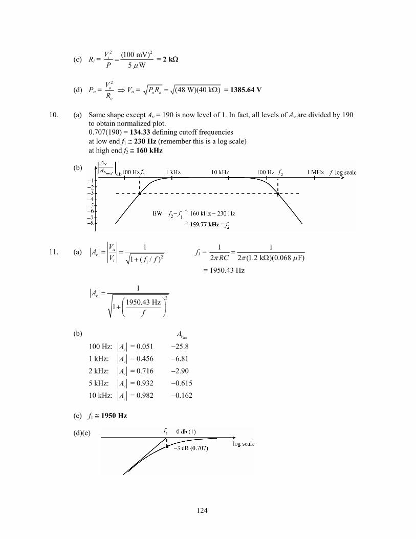
124
(c) Ri = 2 2(100 mV)
5 WiVP μ
= = 2 kΩ
(d) Po = 2
o
o
VR
⇒ Vo = (48 W)(40 k )o oP R = Ω = 1385.64 V
10. (a) Same shape except Av = 190 is now level of 1. In fact, all levels of Av are divided by 190
to obtain normalized plot. 0.707(190) = 134.33 defining cutoff frequencies at low end f1 ≅ 230 Hz (remember this is a log scale) at high end f2 ≅ 160 kHz (b)
11. (a) 2
1
11 ( / )
ov
i
VAV f f
= =+
f1 = 1 12 2 (1.2 k )(0.068 F)RCπ π μ
=Ω
= 1950.43 Hz
2
1
1950.43 Hz1vA
f
=⎛ ⎞
+ ⎜ ⎟⎝ ⎠
(b)
dBVA
100 Hz: vA = 0.051 −25.8 1 kHz: vA = 0.456 −6.81 2 kHz: vA = 0.716 −2.90 5 kHz: vA = 0.932 −0.615 10 kHz: vA = 0.982 −0.162 (c) f1 ≅ 1950 Hz (d)(e)
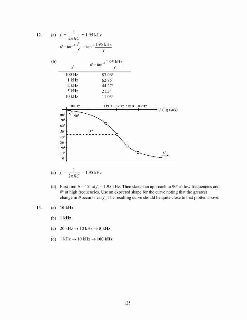
125
12. (a) f1 = 12 RCπ
= 1.95 kHz
θ = tan−1 1ff
= tan−1 1.95 kHzf
(b)
f θ = tan−1 1.95 kHzf
100 Hz 87.06° 1 kHz 62.85° 2 kHz 44.27° 5 kHz 21.3° 10 kHz 11.03°
(c) f1 = 12 RCπ
= 1.95 kHz
(d) First find θ = 45° at f1 = 1.95 kHz. Then sketch an approach to 90° at low frequencies and
0° at high frequencies. Use an expected shape for the curve noting that the greatest change in θ occurs near f1. The resulting curve should be quite close to that plotted above.
13. (a) 10 kHz (b) 1 kHz (c) 20 kHz → 10 kHz → 5 kHz (d) 1 kHz → 10 kHz → 100 kHz
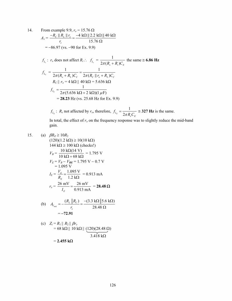
126
14. From example 9.9, re = 15.76 Ω
Av = 4 k 2.2 k 40 k15.76
C L o
e
R R rr
− − Ω Ω Ω=
Ω
= −86.97 (vs. −90 for Ex. 9.9)
sLf : ro does not affect Ri ∴
sLf = 12 ( )s i SR R Cπ +
the same ≅ 6.86 Hz
CLf = 1 1
2 ( ) 2 ( )o L C C o L CR R C R r R Cπ π=
+ +
RC || ro = 4 kΩ || 40 kΩ = 5.636 kΩ
12 (5.636 k 2 k )(1 F)CLf π μ
=Ω + Ω
= 28.23 Hz (vs. 25.68 Hz for Ex. 9.9)
ELf : Re not affected by ro, therefore, 1
2ELe E
fR Cπ
= ≅ 327 Hz is the same.
In total, the effect of ro on the frequency response was to slightly reduce the mid-band gain.
15. (a) βRE ≥ 10R2 (120)(1.2 kΩ) ≥ 10(10 kΩ) 144 kΩ ≥ 100 kΩ (checks!)
VB = 10 k (14 V)10 k 68 k
ΩΩ+ Ω
= 1.795 V
VE = VB − VBE = 1.795 V − 0.7 V = 1.095 V
IE = 1.095 V1.2 k
E
E
VR
=Ω
= 0.913 mA
re = 26 mV 26 mV0.913 mAEI
= = 28.48 Ω
(b) mid
( ) (3.3 k 5.6 k )28.48
L CV
e
R RA
r− Ω Ω
= − =Ω
= −72.91 (c) Zi = R1 || R2 || βre = 68 kΩ || 10 kΩ || (120)(28.48 Ω)
3.418 kΩ = 2.455 kΩ
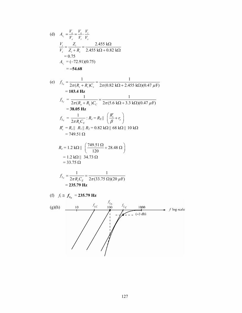
127
(d) s
o o iv
s i s
V V VAV V V
= = ⋅
2.455 k2.455 k 0.82 k
i i
s i s
V ZV Z R
Ω= =
+ Ω + Ω
= 0.75
svA = (−72.91)(0.75) = −54.68
(e) 1 12 ( ) 2 (0.82 k 2.455 k )(0.47 F)SL
s i s
fR R Cπ π μ
= =+ Ω + Ω
= 103.4 Hz
CLf = 1 1
2 ( ) 2 (5.6 k 3.3 k )(0.47 F)o L CR R Cπ π μ=
+ Ω + Ω
= 38.05 Hz
ELf = 1
2 e ER Cπ: Re = RE || s
eR rβ′⎛ ⎞+⎜ ⎟
⎝ ⎠
sR′ = Rs || R1 || R2 = 0.82 kΩ || 68 kΩ || 10 kΩ = 749.51 Ω
Re = 1.2 kΩ || 749.51 28.48 120
Ω⎛ ⎞+ Ω⎜ ⎟⎝ ⎠
= 1.2 kΩ || 34.73 Ω = 33.75 Ω
1 12 2 (33.75 )(20 F)EL
e E
fR Cπ π μ
= =Ω
= 235.79 Hz (f) f1 ≅
ELf = 235.79 Hz (g)(h)
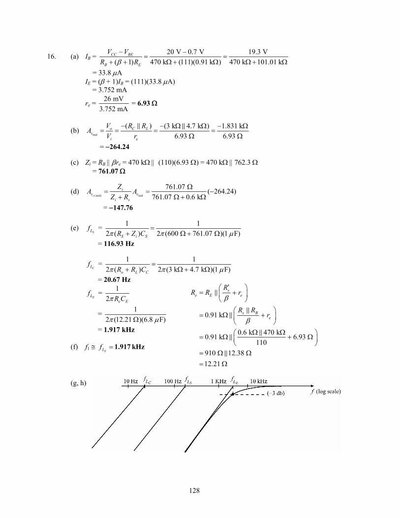
128
0.91 k
0.6 k 470 k0.91 k 6.93 110
910 12.38 12.21
se E e
s Be
RR R r
R Rr
β
β
′⎛ ⎞= +⎜ ⎟
⎝ ⎠⎛ ⎞
= Ω +⎜ ⎟⎝ ⎠
Ω Ω⎛ ⎞= Ω + Ω⎜ ⎟⎝ ⎠
= Ω Ω= Ω
16. (a) IB = 20 V 0.7 V 19.3 V( 1) 470 k (111)(0.91 k ) 470 k 101.01 k
CC BE
B E
V VR Rβ
− −= =
+ + Ω + Ω Ω+ Ω
= 33.8 μA IE = (β + 1)IB = (111)(33.8 μA) = 3.752 mA
re = 26 mV3.752 mA
= 6.93 Ω
(b) mid
( ) (3 k 4.7 k ) 1.831 k6.93 6.93
o C Lv
i e
V R RAV r
− − Ω Ω − Ω= = = =
Ω Ω
= −264.24 (c) Zi = RB || βre = 470 kΩ || (110)(6.93 Ω) = 470 kΩ || 762.3 Ω = 761.07 Ω
(d) ( mid) mid
761.07 ( 264.24)761.07 0.6 ks
iv v
i s
ZA AZ R
Ω= = −
+ Ω + Ω
= −147.76
(e) SLf = 1 1
2 ( ) 2 (600 761.07 )(1 F)S i SR Z Cπ π μ=
+ Ω + Ω
= 116.93 Hz
CLf = 1 1
2 ( ) 2 (3 k 4.7 k )(1 F)o L CR R Cπ π μ=
+ Ω + Ω
= 20.67 Hz
ELf = 1
2 e ER Cπ
= 12 (12.21 )(6.8 F)π μΩ
= 1.917 kHz (f) f1 ≅
ELf = 1.917 kHz (g, h)
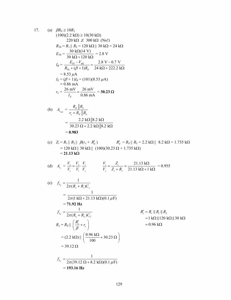
129
1 2
1 k 120 k 30 k0.96 k
s sR R R R′ == Ω Ω Ω= Ω
17. (a) βRE ≥ 10R2 (100)(2.2 kΩ) ≥ 10(30 kΩ) 220 kΩ ≥ 300 kΩ (No!) RTh = R1 || R2 = 120 kΩ || 30 kΩ = 24 kΩ
ETh = 30 k (14 V)30 k 120 k
ΩΩ+ Ω
= 2.8 V
IB = 2.8 V 0.7 V( 1) 24 k 222.2 k
Th BE
Th E
E VR Rβ
− −=
+ + Ω + Ω
= 8.53 μA IE = (β + 1)IB = (101)(8.53 μA) = 0.86 mA
re = 6 mV 26 mV0.86 mAEI
2= = 30.23 Ω
(b) midvA = E L
e E L
R Rr R R+
= 2.2 k 8.2 k
30.23 2.2 k 8.2 kΩ Ω
Ω+ Ω Ω
= 0.983 (c) Zi = R1 || R2 || β(re + ER′ ) ER′ = RE || RL = 2.2 kΩ || 8.2 kΩ = 1.735 kΩ = 120 kΩ || 30 kΩ || (100)(30.23 Ω + 1.735 kΩ) = 21.13 kΩ
(d) svA = o o i
s i s
V V VV V V
= ⋅ 21.13 k21.13 k 1 k
i i
s i s
V ZV Z R
Ω= =
+ Ω + Ω = 0.955
(e) 12 ( )SL
s i s
fR R Cπ
=+
= 12 (1 k 21.13 k )(0.1 F)π μΩ + Ω
= 71.92 Hz
12 ( )CL
o L C
fR R Cπ
=+
Ro = RE || se
R rβ′⎛ ⎞+⎜ ⎟
⎝ ⎠
= (2.2 kΩ) || 0.96 k 30.23 100
Ω⎛ ⎞+ Ω⎜ ⎟⎝ ⎠
= 39.12 Ω
12 (39.12 8.2 k )(0.1 F)CLf π μ
=Ω + Ω
= 193.16 Hz
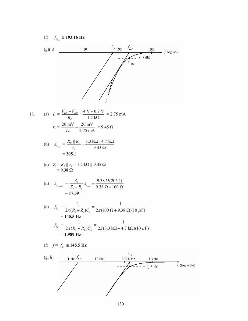
130
(f)
low1f ≅ 193.16 Hz (g)(h)
18. (a) IE = 4 V 0.7 V1.2 k
EE EB
E
V VR− −
=Ω
= 2.75 mA
re = 26 mV 26 mV2.75 mAEI
= = 9.45 Ω
(b) midvA = 3.3 k 4.7 k
9.45 C L
e
R Rr
Ω Ω=
Ω
= 205.1 (c) Zi = RE || re = 1.2 kΩ || 9.45 Ω = 9.38 Ω
(d) ( mid)svA =
mid
9.38 (205.1)9.38 100
iv
i s
Z AZ R
Ω=
+ Ω + Ω
= 17.59
(e) sLf = 1 1
2 ( ) 2 (100 9.38 )(10 F)s i sR Z Cπ π μ=
+ Ω + Ω
= 145.5 Hz
CLf = 1 1
2 ( ) 2 (3.3 k 4.7 k )(10 F)o L ER R Cπ π μ=
+ Ω + Ω
= 1.989 Hz (f) f =
sLf ≅ 145.5 Hz (g, h)
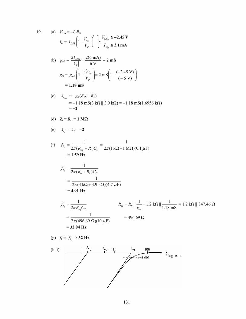
131
Q
Q
GS
D
V
I
≅
≅
2.45 V
2.1 mA
−19. (a) VGS = −IDRS
ID = 2
1 GSDSS
P
VIV
⎛ ⎞−⎜ ⎟
⎝ ⎠
(b) gm0 = 2 2(6 mA)6 V
DSS
P
IV
= = 2 mS
gm = 0( 2.45 V)1 2 mS 1( 6 V)
QGSm
P
Vg
V⎛ ⎞ ⎛ ⎞−− = −⎜ ⎟ ⎜ ⎟⎜ ⎟ −⎝ ⎠⎝ ⎠
= 1.18 mS (c)
midvA = −gm(RD || RL) = −1.18 mS(3 kΩ || 3.9 kΩ) = −1.18 mS(1.6956 kΩ) = −2 (d) Zi = RG = 1 MΩ (e)
svA = Av = −2
(f) sig
1 12 ( ) 2 (1 k 1 M )(0.1 F)GL
i G
fR R Cπ π μ
= =+ Ω + Ω
= 1.59 Hz
12 ( )CL
o L C
fR R Cπ
=+
= 12 (3 k 3.9 k )(4.7 F)π μΩ + Ω
= 4.91 Hz
eq
12SL
S
fR Cπ
= eq1 11.2 k
1.18 mSSm
R Rg
= = Ω = 1.2 kΩ || 847.46 Ω
= 12 (496.69 )(10 F)π μΩ
= 496.69 Ω
= 32.04 Hz (g) f1 ≅
SLf ≅ 32 Hz (h, i)
132
Q
Q
GS
D
V
I
≅
≅
2.55 V
3.3 mA
−
20. (a) same as problem 19
QGSV ≅ −2.45 V, QDI ≅ 2.1 mA
(b) gm0 = 2 mS, gm = 1.18 mS (rd has no effect!) (c)
midvA = −gm (RD || RL || rd) = −1.18 mS(3 kΩ || 3.9 kΩ || 100 kΩ) = −1.18 mS (1.67 kΩ) = −1.971 (vs. −2 for problem 19) (d) Zi = RG = 1 MΩ (the same)
(e) ( mid)svA =
midsig
1 M( )1 M 1 k
iv
i
Z AZ R
Ω=
+ Ω + Ω(−1.971)
= −1.969 vs. −2 for problem 19 (f)
GLf = 1.59 Hz (no effect) :
CLf Ro = RD || rd = 3 kΩ || 100 kΩ = 2.91 kΩ
CLf = 1 1
2 ( ) 2 (2.91 k 3.9 k )(4.7 F)o L CR R Cπ π μ=
+ Ω + Ω
= 4.97 Hz vs. 4.91 Hz for problem 19
SLf : Req =
1 (1 ) /( ( ))S
S m d d D L
RR g r r R R+ + +
= 1.2 k1 (1.2 k )(1 (1.18 mS)(100 k )) /(100 k 3 k 3.9 k )
Ω+ Ω + Ω Ω+ Ω Ω
= 1.2 k1 1.404
Ω+
≅ 499.2 Ω
SLf : =
eq
1 12 2 (499.2 )(10 F)SR Cπ π μ
=Ω
= 31.88 Hz vs. 32.04 for problem 19. Effect of rd = 100 kΩ insignificant!
21. (a) VG = 68 k (20 V)68 k 220 k
ΩΩ+ Ω
= 4.72 V
VGS = VG − IDRS VGS = 4.72 V − ID(2.2 kΩ) ID = IDSS(1 − VGS/VP)2
(b) gm0 = 2 2(10 mA)6 V
DSS
P
IV
= = 3.33 mS
gm = 0( 2.55 V)1 3.33 mS 1
6 VGS
mP
VgV
⎛ ⎞ −⎛ ⎞− = −⎜ ⎟ ⎜ ⎟−⎝ ⎠⎝ ⎠
= 1.91 mS
133
(c) midvA = −gm(RD || RL)
= −(1.91 mS)(3.9 kΩ || 5.6 kΩ) = −4.39 (d) Zi = 68 kΩ || 220 kΩ = 51.94 kΩ
(e) ( mid)svA = o i
i s
V VV V
⋅
i
s
VV
= 51.94 k51.94 k 1.5 k
i
i s
ZZ R
Ω=
+ Ω + Ω = 0.972
( mid)svA = (−4.39)(0.972) = −4.27
(f) sig
1 12 ( ) 2 (1.5 k 51.94 k )(1 F)GL
i G
fR R Cπ π μ
= =+ Ω + Ω
= 2.98 Hz
1 12 ( ) 2 (3.9 k 5.6 k )(6.8 F)CL
o L C
fR R Cπ π μ
= =+ Ω + Ω
= 2.46 Hz
eq
12SL
S
fR Cπ
=
= 12 (388.1 )(10 F)π μΩ
= 41 Hz
Req = RS || 1
mg = 1.5 kΩ || 1
1.91 mS
= 1.5 kΩ || 523.56 Ω = 388.1 Ω
(g) f1 ≅
SLf = 41 Hz (h, i)
134
22. (a)
iHf = 1
12 Th iR Cπ
= 12 (614.56 )(931.92 pF)π Ω
= 277.89 kHz
1 1 2
0.82 k 68 k 10 k 3.418 kTh s iR R R R R=
= Ω Ω Ω Ω
= 0.81 kΩ 2.547 kΩ
= 614.56 Ω Ci =
1(1 )W be bc vC C C A+ + −
= 5 pF + 40 pF + 12 pF(1 − (−72.91)) = 931.92 pF ↑Prob. 15
oHf =
2
12 Th oR Cπ
= 12 (2.08 k )(28 pF)π Ω
= 2.73 MHz
2ThR = RC || RL = 5.6 kΩ || 3.3 kΩ = 2.08 kΩ Co =
o oW ce MC C C+ + = 8 pF + 8 pF + 12 pF = 28 pF
(b) fβ ≅ mid
12 ( )e be bcr C Cπβ +
= 12 (120)(28.48 )(40 pF + 12 pF)π Ω
= 895.56 kHz ↑ Prob. 15 fT = βfβ = (120)(895.56 kHz) = 107.47 MHz (c)
23. (a) 1
12iH
Th i
fR Cπ
=
1ThR = Rs || RB || Ri
Ri: IB = 20 V 0.7 V( 1) 470 k (111)(0.91 k )
CC BE
B E
V VR Rβ
− −=
+ + Ω + Ω
= 33.8 μA IE = (β + 1)IB = (110 + 1)(33.8 μA) = 3.75 mA
re = 26 mV 26 mV3.75 mAEI
= = 6.93 Ω
Ri = βre = (110)(6.93 Ω) = 762.3 Ω
1ThR = Rs || RB || Ri = 0.6 kΩ || 470 kΩ || 762.3 Ω = 335.50 Ω
135
iHf = 1
2 (335.50 )( )iCπ Ω
Ci: Ci = iW beC C+ + (1 − Av)Cbc
Av: midvA = ( ) (4.7 k 3 k )6.93
L C
e
R Rr
− − Ω Ω=
Ω
= −264.2 Ci = 7 pF + 20 pF + (1 − (−264.2)6 pF = 1.62 nF
iHf = 1
2 (335.50 )(1.62 nF)π Ω
≅ 293 kHz
oHf =
2
12 Th oR Cπ
2ThR = RC || RL = 3 kΩ || 4.7 kΩ = 1.831 kΩ
Co =
o oW ce MC C C+ +
≅ Cf = Cbc
= 11 pF + 10 pF + 6 pF
= 27 pF
oHf = 1
2 (1.831 k )(27 pF)π Ω
= 3.22 MHz
(b) fβ = mid
12 ( )e be bcr C Cπβ +
= 12 (110)(6.93 )(20 pF + 6 pF)π Ω
= 8.03 MHz fT = βmidfβ = (110)(8.03 MHz) = 883.3 MHz (c)
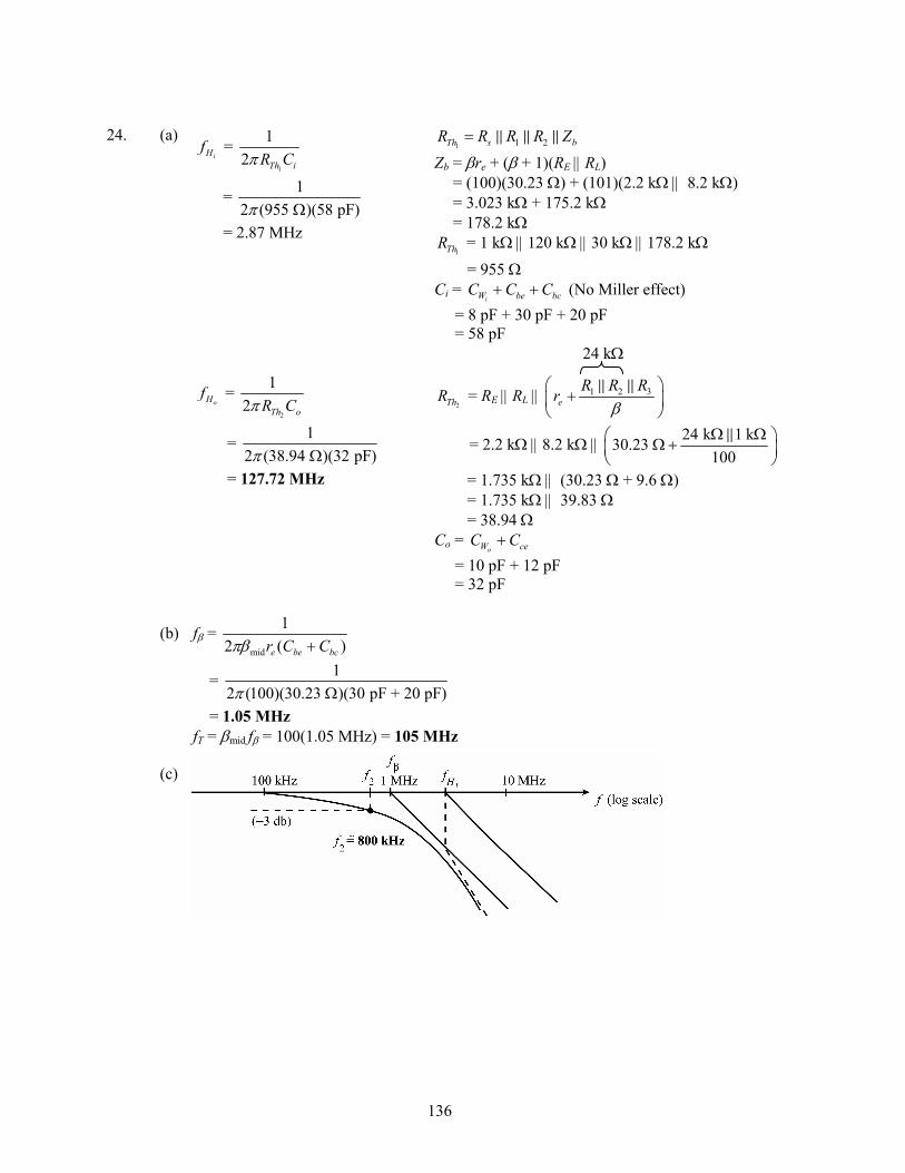
136
24. (a)
iHf = 1
12 Th iR Cπ
= 12 (955 )(58 pF)π Ω
= 2.87 MHz
1 1 2Th s bR R R R Z= Zb = βre + (β + 1)(RE || RL) = (100)(30.23 Ω) + (101)(2.2 kΩ || 8.2 kΩ) = 3.023 kΩ + 175.2 kΩ = 178.2 kΩ
1ThR = 1 kΩ || 120 kΩ || 30 kΩ || 178.2 kΩ = 955 Ω Ci =
iW be bcC C C+ + (No Miller effect) = 8 pF + 30 pF + 20 pF = 58 pF 24 kΩ
oHf =
2
12 Th oR Cπ
= 12 (38.94 )(32 pF)π Ω
= 127.72 MHz
2ThR = RE || RL || 1 2 3e
R R Rrβ
⎛ ⎞+⎜ ⎟
⎝ ⎠
= 2.2 kΩ || 8.2 kΩ || 24 k 1 k30.23 100Ω Ω⎛ ⎞Ω +⎜ ⎟
⎝ ⎠
= 1.735 kΩ || (30.23 Ω + 9.6 Ω) = 1.735 kΩ || 39.83 Ω = 38.94 Ω Co =
oW ceC C+ = 10 pF + 12 pF = 32 pF
(b) fβ = mid
12 ( )e be bcr C Cπβ +
= 12 (100)(30.23 )(30 pF + 20 pF)π Ω
= 1.05 MHz fT = βmid fβ = 100(1.05 MHz) = 105 MHz (c)
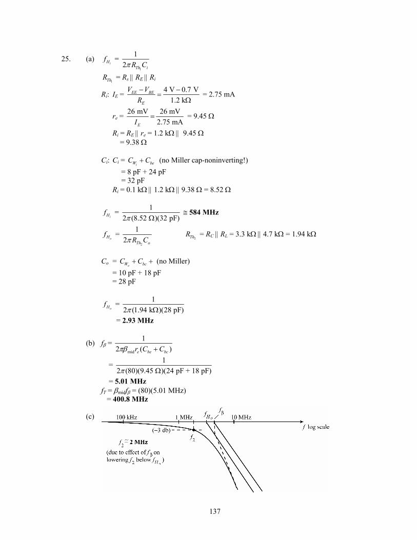
137
25. (a) iHf =
1
12 Th iR Cπ
1ThR = Rs || RE || Ri
Ri: IE = 4 V 0.7 V1.2 k
EE BE
E
V VR− −
=Ω
= 2.75 mA
re = 26 mV 26 mV2.75 mAEI
= = 9.45 Ω
Ri = RE || re = 1.2 kΩ || 9.45 Ω = 9.38 Ω Ci: Ci =
iW beC C+ (no Miller cap-noninverting!) = 8 pF + 24 pF = 32 pF Ri = 0.1 kΩ || 1.2 kΩ || 9.38 Ω = 8.52 Ω
iHf = 1
2 (8.52 )(32 pF)π Ω ≅ 584 MHz
oHf =
2
12 Th oR Cπ
2ThR = RC || RL = 3.3 kΩ || 4.7 kΩ = 1.94 kΩ
Co =
oW bcC C+ + (no Miller) = 10 pF + 18 pF = 28 pF
oHf = 1
2 (1.94 k )(28 pF)π Ω
= 2.93 MHz
(b) fβ = mid
12 ( )e be bcr C Cπβ +
= 12 (80)(9.45 )(24 pF + 18 pF)π Ω
= 5.01 MHz fT = βmidfβ = (80)(5.01 MHz) = 400.8 MHz (c)
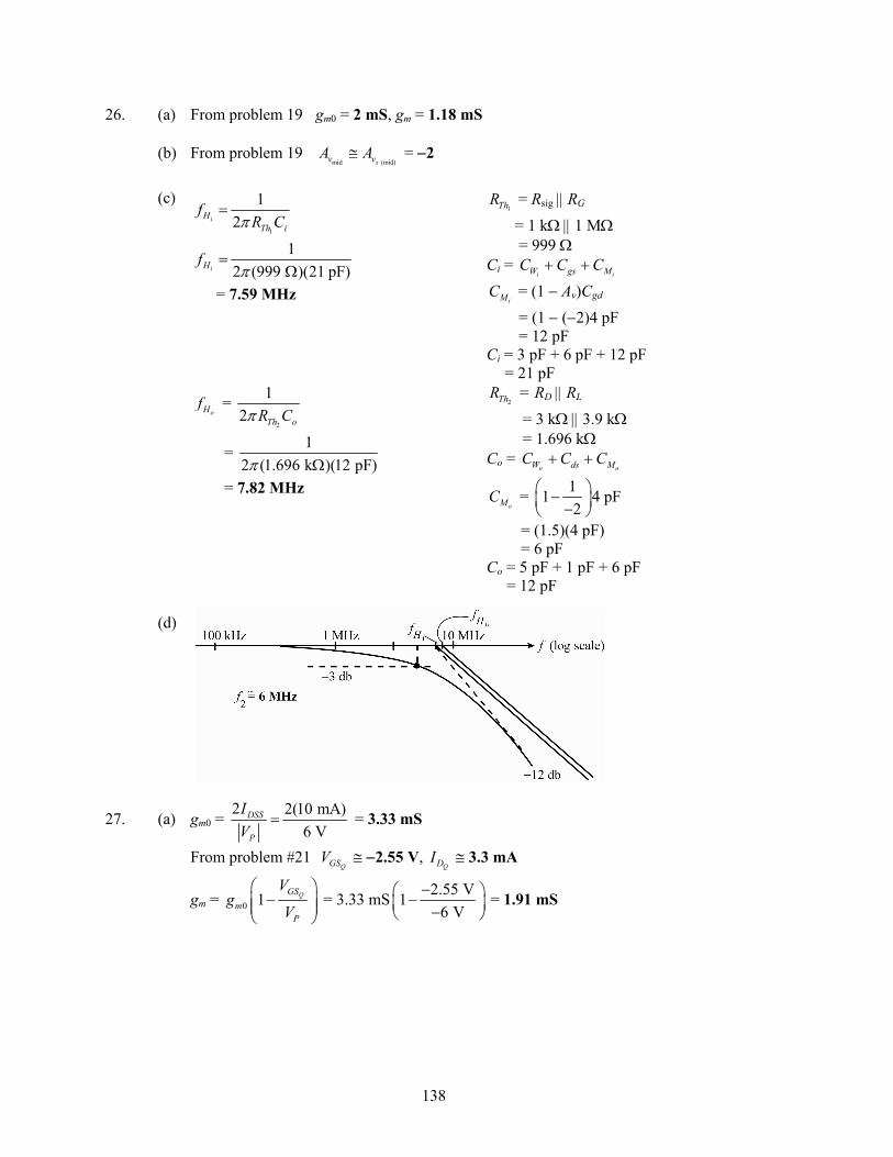
138
26. (a) From problem 19 gm0 = 2 mS, gm = 1.18 mS (b) From problem 19
mid (mid)sv vA A≅ = −2
(c)
1
12iH
Th i
fR Cπ
=
12 (999 )(21 pF)iHf π
=Ω
= 7.59 MHz
1ThR = Rsig || RG = 1 kΩ || 1 MΩ = 999 Ω Ci =
i iW gs MC C C+ +
iMC = (1 − Av)Cgd = (1 − (−2)4 pF = 12 pF Ci = 3 pF + 6 pF + 12 pF = 21 pF
oHf =
2
12 Th oR Cπ
= 12 (1.696 k )(12 pF)π Ω
= 7.82 MHz
2ThR = RD || RL = 3 kΩ || 3.9 kΩ = 1.696 kΩ Co =
o oW ds MC C C+ +
oMC = 11 4 pF2
⎛ ⎞−⎜ ⎟−⎝ ⎠
= (1.5)(4 pF) = 6 pF Co = 5 pF + 1 pF + 6 pF = 12 pF
(d)
27. (a) gm0 = 2 2(10 mA)6 V
DSS
P
IV
= = 3.33 mS
From problem #21 QGSV ≅ −2.55 V,
QDI ≅ 3.3 mA
gm = 0 1 QGSm
P
Vg
V⎛ ⎞−⎜ ⎟⎜ ⎟
⎝ ⎠ = 3.33 mS 2.55 V1
6 V−⎛ ⎞−⎜ ⎟−⎝ ⎠
= 1.91 mS
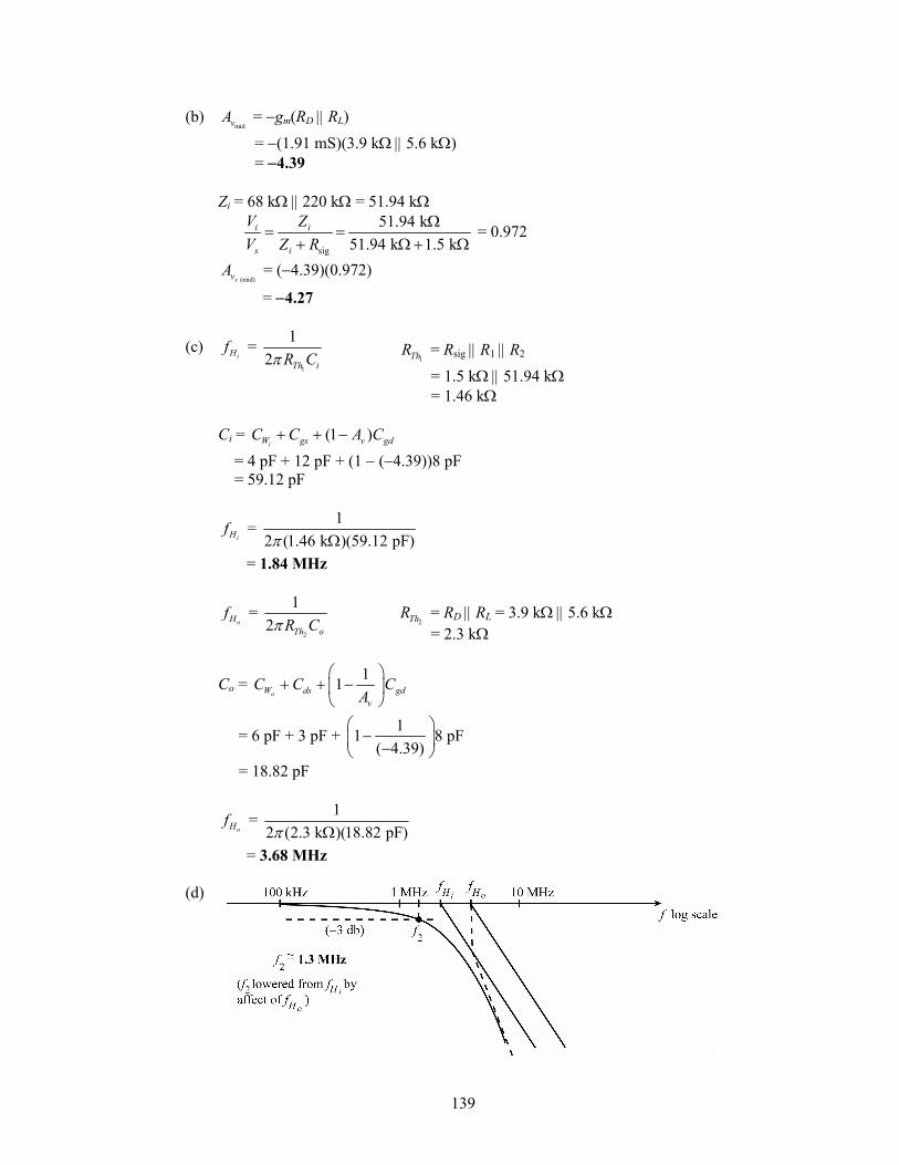
139
(b) midvA = −gm(RD || RL)
= −(1.91 mS)(3.9 kΩ || 5.6 kΩ) = −4.39 Zi = 68 kΩ || 220 kΩ = 51.94 kΩ
sig
51.94 k51.94 k 1.5 k
i i
s i
V ZV Z R
Ω= =
+ Ω + Ω = 0.972
(mid)svA = (−4.39)(0.972)
= −4.27
(c) iHf =
1
12 Th iR Cπ
1ThR = Rsig || R1 || R2
= 1.5 kΩ || 51.94 kΩ = 1.46 kΩ
Ci = (1 )
iW gs v gdC C A C+ + − = 4 pF + 12 pF + (1 − (−4.39))8 pF = 59.12 pF
iHf = 1
2 (1.46 k )(59.12 pF)π Ω
= 1.84 MHz
oHf =
2
12 Th oR Cπ
2ThR = RD || RL = 3.9 kΩ || 5.6 kΩ
Co = 11oW ds gd
v
C C CA
⎛ ⎞+ + −⎜ ⎟
⎝ ⎠
= 6 pF + 3 pF + 11 8 pF( 4.39)
⎛ ⎞−⎜ ⎟−⎝ ⎠
= 18.82 pF
oHf = 1
2 (2.3 k )(18.82 pF)π Ω
= 3.68 MHz (d)
= 2.3 kΩ
140
28. TvA =
1 2 3 4v v v vA A A A⋅ ⋅ ⋅ = Av
4 = (20)4 = 16 × 104
29. 2f ′ = ( )1/22 1n f−
= ( )1/ 42 1 (2.5 MHz)−
1.18 = 0.435(2.5 MHz) = 1.09 MHz
30. 11 1/ 1/4
40 Hz2 1 2 1n
ff ′= =− −
= 40 Hz0.435
= 91.96 Hz
31. (a) v = 4π
Vm1 1sin 2 sin 2 (3 ) sin 2 (5 )3 5s s sf t f t f tπ π π⎡ + +⎢⎣
1 1sin 2 (7 ) sin 2 (9 )7 9s sf t f tπ π ⎤+ + + ⎥⎦
…
= 12.73 × 10⁻³ 3 31(sin 2 (100 10 ) sin 2 (300 10 )3
t tπ π× + ×
3 3 31 1 1sin 2 (500 10 ) sin 2 (700 10 ) sin 2 (900 10 ) )5 7 9
t t tπ π π+ × + × + ×
(b) BW ≅ 0.35
rt
≅ 0.350.7 sμ
tr ≅ 0.75 μs − 0.05 μs = 0.7 μs
≅ 500 kHz
(c) P = 90 mV 80 mV90 mV
V VV
′− −= = 0.111
(0.111)(100 kHz)oL s
Pf fπ π
= = ≅ 3.53 kHz
At 90% or 81 mV, t ≅ 0.75 μs At 10% or 9 mV, t ≅ 0.05 μs
141
Chapter 10
1. Vo = 11
250 k (1.5 V)20 k
FR VR
Ω− = −
Ω = −18.75 V
2. Av = 1
o F
i
V RV R
= −
For R1 = 10 kΩ:
Av = 500 k10 k
Ω−
Ω = −50
For R1 = 20 kΩ:
Av = 500 k20 k
Ω−
Ω = −25
3. Vo = 11
1 M20 k
fRV
RΩ⎛ ⎞− = −⎜ ⎟Ω⎝ ⎠
V1 = 2 V
V1 = 2 V50−
= −40 mV
4. Vo = 1 11
200 k20 k
FR V VR
Ω− = −
Ω = −10 V1
For V1 = 0.1 V: Vo = −10(0.1 V) = −1 V Vo ranges For V1 = 0.5 V: from Vo = −10(0.5 V) = −5 V −1 V to −5 V
5. Vo = 11
360 k1 1 ( 0.3 V)12 k
FR VR
⎛ ⎞ Ω⎛ ⎞+ = + −⎜ ⎟ ⎜ ⎟Ω⎝ ⎠⎝ ⎠
= 31(−0.3 V) = −9.3 V
6. Vo = 1 11
360 k1 112 k
FR V VR
⎛ ⎞ Ω⎛ ⎞+ = +⎜ ⎟ ⎜ ⎟Ω⎝ ⎠⎝ ⎠ = 2.4 V
V1 = 2.4 V31
= 77.42 mV
142
7. Vo = 11
1 FR VR
⎛ ⎞+⎜ ⎟
⎝ ⎠
For R1 = 10 kΩ:
Vo = 200 k1 (0.5 V)10 k
Ω⎛ ⎞+⎜ ⎟Ω⎝ ⎠ = 21(0.5 V) = 10.5 V
For R1 = 20 kΩ:
Vo = 200 k120 k
Ω⎛ ⎞+⎜ ⎟Ω⎝ ⎠(0.5 V) = 11(0.5 V) = 5.5 V
Vo ranges from 5.5 V to 10.5 V.
8. Vo = 1 2 31 2 3
f f fR R RV V V
R R R⎡ ⎤
− + +⎢ ⎥⎣ ⎦
= 330 k 330 k 330 k(0.2 V) + ( 0.5 V)+ (0.8 V)33 k 22 k 12 k
Ω Ω Ω⎡ ⎤− −⎢ ⎥Ω Ω Ω⎣ ⎦
= −[10(0.2 V) + 15(−0.5 V) + 27.5(0.8 V)] = −[2 V + (−7.5 V) + 2.2 V] = −[24 V − 7.5 V] = −16.5 V
9. Vo = 1 2 31 2 3
F F FR R RV V VR R R
⎡ ⎤− + +⎢ ⎥⎣ ⎦
= 68 k 68 k 68 k(0.2 V)+ ( 0.5 V) + ( 0.8 V) 33 k 22 k 12 k
Ω Ω Ω⎡ ⎤− − +⎢ ⎥Ω Ω Ω⎣ ⎦
= −[0.41 V − 1.55 V + 4.53 V] = −3.39 V
10. vo(t) = 11 ( )v t dt
RC− ∫
= 1 1.5 (200 k )(0.1 F)
dtμ
−Ω ∫
= −50(1.5t) = −75t 11. Vo = V1 = +0.5 V
12. Vo = 11
100 k20 k
fRV
RΩ
− = −Ω
(1.5 V)
= −5(1.5 V) = −7.5 V
13. V2 = 200 k (0.2 V)20 k
Ω⎡ ⎤− ⎢ ⎥Ω⎣ ⎦ = −2 V
V3 = 200 k1 (0.2 V)10 k
Ω⎛ ⎞+⎜ ⎟Ω⎝ ⎠ = +4.2 V
143
14. Vo = 400 k 100 k 100 k1 (0.1 V) (0.1 V)20 k 20 k 10 k
Ω − Ω Ω⎛ ⎞ ⎛ ⎞ ⎛ ⎞+ ⋅ + −⎜ ⎟ ⎜ ⎟ ⎜ ⎟Ω Ω Ω⎝ ⎠ ⎝ ⎠ ⎝ ⎠
= (2.1 V)(−5) + (−10)(0.1 V) = −10.5 V − 1 V = −11.5 V
15. Vo = − 600 k 600 k 300 k(25 mV) + ( 20 mV)15 k 30 k 30 k
Ω Ω Ω⎡ ⎤⎛ ⎞− −⎜ ⎟⎢ ⎥Ω Ω Ω⎣ ⎦⎝ ⎠
300 k ( 20 mV)15 k
⎡ ⎤Ω⎛ ⎞+ − −⎜ ⎟⎢ ⎥Ω⎝ ⎠⎣ ⎦
= −[40(25 mV) + (20)(−20 mV)](−10) + (−20)(−20 mV) = −[1 V − 0.4 V](−10) + 0.4 V = 6 V + 0.4 V = 6.4 V
16. Vo = 1
1 fIo Io f
RV I R
R⎛ ⎞+ +⎜ ⎟
⎝ ⎠
= 200 k1 (6 mV) + (120 nA)(200 k )2 k
Ω⎛ ⎞+ Ω⎜ ⎟Ω⎝ ⎠
= 101(6 mV) + 24 mV = 606 mV + 24 mV = 630 mV
17. 4 nA20 nA + 2 2Io
IB IB
II I ++ = + = = 22 nA
4 nA20 nA 2 2Io
IB IB
II I −− = − = − = 18 nA
18. f1 = 800 kHz
fc = 2
13
800 kHz150 10v
fA
=×
= 5.3 Hz
19. ACL = 2.4 V/ s/ 0.3 V/10 si
SRV t
μμ
=Δ Δ
= 80
20. ACL = 1
200 k2 k
fRR
Ω=
Ω = 100
K = ACL Vi = 100(50 mV) = 5 V
ws ≤ 0.4 V / s5 V
SRK
μ= = 80 × 103 rad/s
fs = 380 10
2 2swπ π
×= = 12.73 kHz
144
21. VIo = 1 mV, typical IIo = 20 nA, typical
Vo(offset) = 1
1 fIo
RV
R⎛ ⎞+⎜ ⎟
⎝ ⎠ + IIoRf
= 200 k1 (1 mV) 20 k
Ω⎛ ⎞+⎜ ⎟Ω⎝ ⎠ + (200 kΩ)(20 nA)
= 101(1 mV) + 4000 × 10−6 = 101 mV + 4 mV = 105 mV 22. Typical characteristics for 741 Ro = 25 Ω, A = 200 K
(a) ACL = 1
200 k2 k
fRR
Ω− = −
Ω = −100
(b) Zi = R1 = 2 kΩ
(c) Zo = 25 11 1 (200,000)
100
oRAβ
Ω=
+ +
= 25 2001
Ω = 0.0125 Ω
23. Ad = 120 mV1 mV
o
d
VV
= = 120
Ac = 20 V1 mV
o
c
VV
μ= = 20 × 10−3
Gain (dB) = 20 log 3
12020log20 10
d
c
AA −=
×
= 20 log(6 × 10³) = 75.56 dB
145
24. Vd = Vi1 − Vi2 = 200 μV − 140 μV = 60 μV
Vc = 1 2 (200 V 140 V)2 2
i iV V μ μ+ += = 170 μV
(a) CMRR = d
c
AA
= 200
Ac = 6000200 200
dA= = 30
(b) CMRR = 510d
c
AA
=
Ac = 5 5
600010 10
dA= = 0.06 = 60 × 10−3
Using Vo = AdVd11 c
d
VCMRR V
⎡ ⎤+⎢ ⎥
⎣ ⎦
(a) Vo = 6000(60 μV) 1 170 V1200 60 V
μμ
⎡ ⎤+⎢ ⎥
⎣ ⎦ = 365.1 mV
(b) Vo = 6000(60 μV) 5
1 170 V110 60 V
μμ
⎡ ⎤+⎢ ⎥
⎣ ⎦ = 360.01 mV
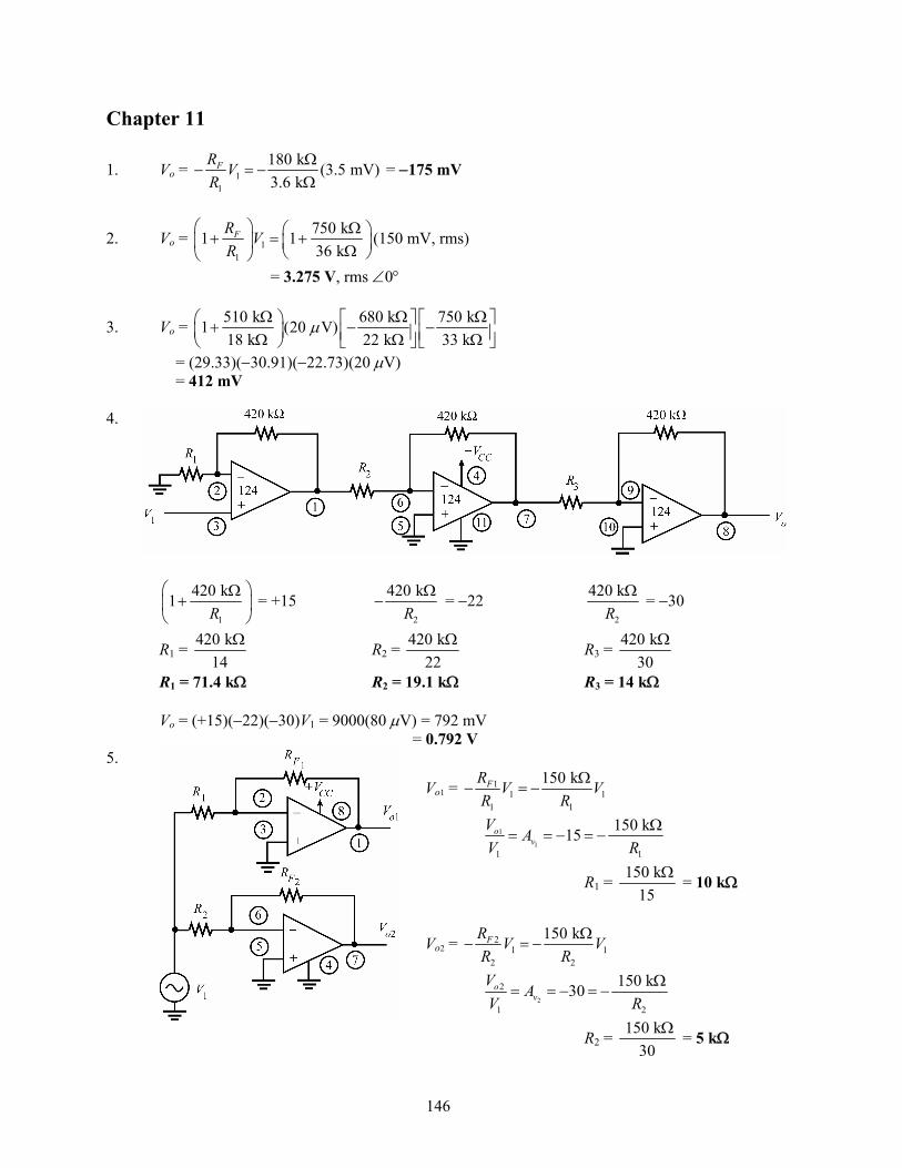
146
Chapter 11
1. Vo = 11
180 k (3.5 mV)3.6 k
FR VR
Ω− = −
Ω = −175 mV
2. Vo = 11
750 k1 136 k
FR VR
⎛ ⎞ Ω⎛ ⎞+ = +⎜ ⎟ ⎜ ⎟Ω⎝ ⎠⎝ ⎠(150 mV, rms)
= 3.275 V, rms ∠0°
3. Vo = 510 k 680 k 750 k1 (20 V)18 k 22 k 33 k
μΩ Ω Ω⎛ ⎞ ⎡ ⎤ ⎡ ⎤+ − −⎜ ⎟ ⎢ ⎥ ⎢ ⎥Ω Ω Ω⎝ ⎠ ⎣ ⎦ ⎣ ⎦
= (29.33)(−30.91)(−22.73)(20 μV) = 412 mV 4.
1
420 k1R
⎛ ⎞Ω+⎜ ⎟
⎝ ⎠ = +15
2
420 kR
Ω− = −22
2
420 kR
Ω = −30
R1 = 420 k14
Ω R2 = 420 k22
Ω R3 = 420 k30
Ω
R1 = 71.4 kΩ R2 = 19.1 kΩ R3 = 14 kΩ Vo = (+15)(−22)(−30)V1 = 9000(80 μV) = 792 mV = 0.792 V 5.
Vo1 = 11 1
1 1
150 kFR V VR R
Ω− = −
1
1
1 1
150 k15ov
V AV R
Ω= = − = −
R1 = 150 k15
Ω = 10 kΩ
Vo2 = 21 1
2 2
150 kFR V VR R
Ω− = −
2
2
1 2
150 k30ov
V AV R
Ω= = − = −
R2 = 150 k30
Ω = 5 kΩ
147
6. Vo = 1 21 2
470 k 470 k(40 mV) + (20 mV)47 k 12 k
F FR RV VR R
⎡ ⎤ Ω Ω⎡ ⎤− + = −⎢ ⎥ ⎢ ⎥Ω Ω⎣ ⎦⎣ ⎦
= −[400 mV + 783.3 mV] = −1.18 V
7. Vo = 1 210 k 150 k 300 k 300 k
10 k 10 k 150 k 150 kV VΩ Ω+ Ω Ω⎛ ⎞⎛ ⎞ −⎜ ⎟⎜ ⎟Ω + Ω Ω Ω⎝ ⎠⎝ ⎠
= 0.5(3)(1 V) − 2(2 V) = 1.5 V − 4 V = −2.5 V
8. Vo = 330 k 470 k 470 k(12 mV) (18 mV)33 k 47 k 47 k
⎧ ⎫Ω Ω Ω⎡ ⎤⎛ ⎞− +⎨ ⎬⎜ ⎟⎢ ⎥Ω Ω Ω⎣ ⎦⎝ ⎠⎩ ⎭
= −[(−120 mV)(10) + 180 mV] = −[−1.2 V + 0.18 V] = +1.02 V 9. 10.
11. IL = 1
1
12 V2 k
VR
=Ω
= 6 mA
12. Vo = −I1R1 = −(2.5 mA)(10 kΩ) = −25 V
13. 1 1
1o F
s
I RV R R
⎛ ⎞= ⎜ ⎟
⎝ ⎠
100 k 1 (10 mV)200 k 10 oI Ω ⎛ ⎞= ⎜ ⎟Ω Ω⎝ ⎠
= 0.5 mA
14. Vo = 21p
RR
⎛ ⎞+⎜ ⎟⎜ ⎟
⎝ ⎠[V2 − V1]
= 2(5000)1 [1 V 3 V]1000
⎛ ⎞+ −⎜ ⎟⎝ ⎠
= −22 V
148
15. fOH = 1 1
1 12 2 (2.2 k )(0.05 F)R Cπ π μ
=Ω
= 1.45 kHz
16. fOL = 1 1
1 12 2 (20 k )(0.02 F)R Cπ π μ
=Ω
= 397.9 Hz
17. fOL = 1 1
1 12 2 (10 k )(0.05 F)R Cπ π μ
=Ω
= 318.3 Hz
fOH = 2 2
1 12 2 (20 k )(0.02 F)R Cπ π μ
=Ω
= 397.9 Hz
149
Chapter 12
1. 18 V 0.7 V1.2 kQ
CC BEB
B
V VIR− −
= =Ω
= 14.42 mA
Q QC BI Iβ= = 40(14.42 mA) = 576.67 mA
Pi = VCCIdc ≅ QCC CV I = (18 V)(576.67 mA)
≅ 10.4 W IC(rms) = βIB(rms) = 40(5 mA) = 200 mA Po = 2 (rms)C CI R = (200 mA)2(16 Ω) = 640 mW
2. QBI = 18 V 0.7 V
1.5 kCC BE
B
V VR− −
=Ω
= 11.5 mA
QCI =
QBIβ = 40(11.5 mA) = 460 mA
Pi(dc) = VCCIdc = ( )Q QCC C BV I I+
= 18 V(460 mA + 11.5 mA) = 8.5 W
= 18 V(460 mA) = 8.3 WQi CC CP V I⎡ ⎤≈⎣ ⎦
3. From problem 2:
QCI = 460 mA, Pi = 8.3 W. For maximum efficiency of 25%:
%η = 100% × o
i
PP
= 8.3 W
oP × 100% = 25%
Po = 0.25(8.3 W) = 21 W [If dc bias condition also is considered: VC = VCC −
QC CI R = 18 V − (460 mA)(16 Ω) = 10.64 V
collector may vary ±7.36 V about Q-point, resulting in maximum output power:
Po = 2 2( ) (7.36 V)2 2(16)CE
C
V PR
= = 1.69 W
150
4. Assuming maximum efficiency of 25% with Po(max) = 1.5 W
%η = o
i
PP
× 100%
Pi = 1.5 W0.25
= 6 W
Assuming dc bias at mid-point, VC = 9 V
18 V 9 V16 Q
CC CC
C
V VIR− −
= =Ω
= 0.5625 A
Pi(dc) = QCC CV I = (18 V)(0.5625 A)
= 10.38 W at this input:
%η = o
i
PP
× 100% = 1.5 W10.38 W
× 100% = 14.45%
5. Rp = 2
1
2s
N RN
⎛ ⎞⎜ ⎟⎝ ⎠
= 225 (4 )
1⎛ ⎞ Ω⎜ ⎟⎝ ⎠
= 2.5 kΩ
6. R2 = a2R1
a2 = 2
1
8 k8
RR
Ω=
Ω = 1000
a = 1000 = 31.6 7. R2 = a2R1 8 kΩ = a2(4 Ω)
a2 = 8 k4 ΩΩ
= 2000
a = 2000 = 44.7 8. (a) Ppri = PL = 2 W
(b) PL = 2
L
L
VR
VL = (2 W)(16 )L LP R = Ω
= 32 = 5.66 V (c) R2 = a2R1 = (3.87)2(16 Ω) = 239.6 Ω
Ppri = 2pri
pri
VR
= 2 W
2priV = (2 W)(239.6 Ω)
Vpri = 479.2 = 21.89 V [or, Vpri = aVL = (3.87)(5.66 V) = 21.9 V]
151
(d) PL = 2L LI R
IL = 2 W16
L
L
PR
=Ω
= 353.55 mA
Ppri = 2 W = 2pri priI R = (239.6 Ω) 2
priI
Ipri = 2 W239.6 Ω
= 91.36 mA
or, Ipri = 353.55 mA3.87
LIa= = 91.36 mA
9. Idc =
QCI = 150 mA
Pi = QCC CV I = (36 V)(150 mA) = 5.4 W
%η = 2 W100% 100%5.4 W
o
i
PP× = × = 37%
10. 11.
152
12. (a) Pi = VCCIdc = (25 V)(1.75 A) = 43.77 W
Where, Idc = 2 2 2 22 V8
pp
L
VI
Rπ π π= = ⋅
Ω = 1.75 A
(b) Po = 2 2(22 V)
2 2(8 )p
L
VR
=Ω
= 30.25 W
(c) %η = o
i
PP
× 100% = 30.75 W43.77 W
× 100% = 69%
13. (a) max Pi = VCCIdc
= VCC ⋅ 2 2 25 V(25 V)8
CC
L
VRπ π
⎛ ⎞ ⎡ ⎤⋅ = ⋅⎜ ⎟ ⎢ ⎥Ω⎣ ⎦⎝ ⎠
= 49.74 W
(b) max Po = 2 2(25 V)
2 2(8 )CC
L
VR
=Ω
= 39.06 W
(c) max %η = max 39.06 W100%max 49.74 W
o
i
PP× = × 100%
= 78.5% 14. (a)
(peak)LV = 20 V
Pi = VCCIdc = 2 LCC
L
VVRπ
⎡ ⎤⋅⎢ ⎥
⎣ ⎦
= 2 20 V(22 V)4 π
⎡ ⎤⋅⎢ ⎥Ω⎣ ⎦ = 70 W
Po = 2 2(20 V)
2 2(4 )L
L
VR
=Ω
= 50 W
%η = o
i
PP
× 100% = 50 W70 W
× 100% = 71.4%
(b) Pi = 2 4 V(22 V)4 π
⎡ ⎤⋅⎢ ⎥Ω⎣ ⎦ = 14 W
Po = 2(4)
2(4) = 2 W
%η = o
i
PP
× 100% = 2 W14 W
× 100% = 14.3%
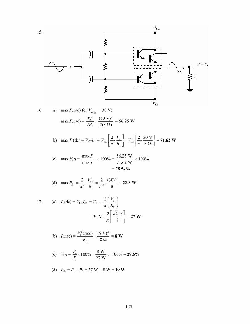
153
15. 16. (a) max Po(ac) for
peakLV = 30 V:
max Po(ac) = 2 2(30 V)
2 2(8 )L
L
VR
=Ω
= 56.25 W
(b) max Pi(dc) = VCCIdc = 2 2 30 V8
oCC CC
L
VV VRπ π
⎡ ⎤ ⎡ ⎤⋅ = ⋅⎢ ⎥ ⎢ ⎥Ω⎣ ⎦⎣ ⎦ = 71.62 W
(c) max %η = maxmax
o
i
PP
× 100% = 56.25 W71.62 W
× 100%
= 78.54%
(d) max2 2
2 2
2 2 (30)8Q
CCZ
L
VPRπ π
= ⋅ = ⋅ = 22.8 W
17. (a) Pi(dc) = VCCIdc = VCC ⋅ 2 o
L
VRπ
⎛ ⎞⎜ ⎟⎝ ⎠
= 30 V ⋅ 2 2 88π
⎡ ⎤⋅⎢ ⎥⎣ ⎦
= 27 W
(b) Po(ac) = 2 2(rms) (8 V)
8 L
L
VR
=Ω
= 8 W
(c) %η = 8 W100%27 W
o
i
PP× = × 100% = 29.6%
(d) P2Q = Pi − Po = 27 W − 8 W = 19 W
154
18. (a) Po(ac) = 2 2(rms) (18 V)
8 L
L
VR
=Ω
= 40.5 W
(b) Pi(dc) = VCCIdc = peak2 LCC
L
VV
Rπ⎡ ⎤
⋅⎢ ⎥⎢ ⎥⎣ ⎦
= (40 V) 2 18 2 V8 π
⎡ ⎤⋅⎢ ⎥Ω⎣ ⎦
= 81 W
(c) %η = o
i
PP
× 100% = 40.5 W81 W
× 100% = 50%
(d) 2Q
P = Pi − Po = 81 W − 40.5 W = 40.5 W
19. %D2 = 2
1
AA
× 100% = 0.3 V2.1 V
× 100% ≅ 14.3%
%D3 = 3
1
AA
× 100% = 0.1 V2.1 V
× 100% ≅ 4.8%
%D4 = 4
1
AA
× 100% = 0.05 V2.1 V
× 100% ≅ 2.4%
20. %THD = 2 2 2
2 3 4D D D+ + × 100%
= 2 2 2(0.143) (0.048) (0.024)+ + × 100% = 15.3%
21. D2 = ( )max min
max min
12 CE CE
CE CE
V V
V V
+
− × 100%
=
1 (20 V + 2.4 V) 10 V2
20 V 2.4 V
−
− × 100%
= 1.2 V17.6 V
× 100% = 6.8%
22. THD = 2 2 2 2 2 2
2 3 4 (0.15) (0.01) (0.05)D D D+ + = + + ≅ 0.16
P1 = 2 2
1 (3.3 A) (4 )2 2
CI R Ω= = 21.8 W
P = (1 + THD2)P1 = [1 + (0.16)2)]21.8 W = 22.36 W
155
23. PD (150°C) = PD(25°C) − (T150 − T25) (Derating Factor) = 100 W − (150°C − 25°C)(0.6 W/°C) = 100 W − 125(0.6) = 100 − 75 = 25 W
24. PD = 200 C 80 C0.5 C/W + 0.8 C/W + 1.5 C/W
J A
JC CS SA
T Tθ θ θ
− ° − °=
+ + ° ° °
= 120 C2.8 C/W
°°
= 42.9 W
25. PD = J A
JA
T Tθ−
= 200 C 80 C 120 C(40 C/W) 40 C/W° − ° °
=° °
= 3 W
156
Chapter 13 1. 2. 3. 4. 5.
157
6. 7. Circuit operates as a window detector.
Output goes low for input above 9.1 k ( 12 V)9.1 k + 6.2 k
Ω+
Ω Ω = 7.1 V
Output goes low for input below 1 k ( 12 V)1 k + 6.2 k
Ω+
Ω Ω = 1.7 V
Output is high for input between +1.7 V and +7.1 V. 8.
9. 5
11010 26(16 V) = (16 V)2 32
= 13 V
10. Resolution = 12
10 V 10 V2 2 4096REF
n
V= = = 2.4 mV/count
11. See section 13.3. 12. Maximum number of count steps = 212 = 4096
13. 212 = 4096 steps at T = 1 120 MHzf
= = 50 ns/count
Period = 4096 counts × ns50count
= 204.8 μs
158
14.
f = 1.44( 2 )A BR R C+
= 350 kHz
C = 1.447.5 k + 2(7.5 k )(350 kHz)Ω Ω
≅ 183 pF 15.
T = 1.1 RAC 20 μs = 1.1(7.5 kΩ)C
C = 6
3
20 101.1(7.5 10 )
−××
= 2.4 × 10−9 = 2400 × 10−12 = 2400 pF
16. T = 1 110 kHzf
= = 100 μs
T = 1.1 RAC = 1.1(5.1 kΩ)(5 nF) = 28 μs
159
17. fo = 1 1
2 CV VR C V
+
+
⎛ ⎞−⎜ ⎟⎝ ⎠
V+ = 12 V
VC = 3
2 3
11 k( ) ( 12 V)1.8 k + 11 k
R VR R
+ Ω= +
+ Ω Ω = 10.3 V
fo = 2 12 V 10.3 V(4.7 k )(0.001 F) 12 Vμ
−⎡ ⎤⎢ ⎥Ω ⎣ ⎦
= 60.3 × 10³ ≅ 60 kHz 18. With potentiometer set at top:
VC = 3 4
2 3 4
5 k 18 k (12 V)510 5 k 18 k
R R VR R R
++ Ω + Ω=
+ + Ω + Ω+ Ω = 11.74 V
resulting in a lower cutoff frequency of
fo = 31 1
2 2 12 V 11.74 V(10 10 )(0.001 F) 12 V
CV VR C V μ
+
+
⎛ ⎞− −⎛ ⎞=⎜ ⎟ ⎜ ⎟× ⎝ ⎠⎝ ⎠
= 4.3 kHz With potentiometer set at bottom:
VC = 4
2 3 4
18 k (12 V)510 5 k 18 k
R VR R R
+ Ω=
+ + Ω + Ω + Ω
= 9.19 V resulting in a higher cutoff frequency of
fo = 1 1
2 2 12 V 9.19 V(10 k )(0.001 F) 12 V
CV VR C V μ
+
+
⎛ ⎞− −⎡ ⎤=⎜ ⎟ ⎢ ⎥Ω ⎣ ⎦⎝ ⎠
= 61.2 kHz 19. V+ = 12 V
VC = 3
2 3
10 k (12 V)1.5 k + 10 k
R VR R
+ Ω=
+ Ω Ω = 10.4 V
fo = 1 1 1
2 2 12 V 10.4 V10 k ( ) 12 V
CV VR C V C
+
+
⎛ ⎞− −⎛ ⎞=⎜ ⎟ ⎜ ⎟Ω ⎝ ⎠⎝ ⎠
= 200 kHz
C1 = 2 (0.133)10 k (200 kHz)Ω
= 133 × 10−12 = 133 pF
20. fo = 1 1
0.3 0.3(4.7 k )(0.001 F)R C μ
=Ω
= 63.8 kHz
21. C1 = 1
0.3 0.3(10 k )(100 kHz)R f
=Ω
= 300 pF
160
22. fL = ± 8 ofV
= ±38(63.8 10 )
6 V×
1 1
0.3 0.34.7 k (0.001 F)of R C μ
⎡ ⎤= =⎢ ⎥Ω⎣ ⎦
= 85.1 kHz = 63.8 kHz 23. For current loop: mark = 20 mA space = 0 mA For RS − 232 C: mark = −12 V space = +12 V 24. A line (or lines) onto which data bits are connected. 25. Open-collector is active-LOW only. Tri-state is active-HIGH or active-LOW.
161
Chapter 14
1. Af = 2000 200011 2011 ( 2000)
10
AAβ
− −= =
+ ⎛ ⎞+ − −⎜ ⎟⎝ ⎠
= −9.95
2. ( )
1 1 (10%)1 100020
f
f
dA dAA A Aβ
= =⎛ ⎞− −⎜ ⎟⎝ ⎠
= 0.2%
3. Af = 300 30011 211 ( 300)
15
AAβ
− −= =
+ ⎛ ⎞+ − −⎜ ⎟⎝ ⎠
= −14.3
Rif = (1 + βA)Ri = 21(1.5 kΩ) = 31.5 kΩ
Rof = 50 k1 21
oRAβ
Ω=
+ = 2.4 kΩ
4. RL = o D
o D
R RR R+
= 40 kΩ || 8 kΩ = 6.7 kΩ
A = −gmRL = −(5000 × 10−6)(6.7 × 10³) = −33.5
β = 2
1 2
200 k200 k 800 k
RR R− − Ω
=+ Ω + Ω
= −0.2
Af = 33.5 33.51 1 ( 0.2)( 33.5) 7.7
AAβ
− −= =
+ + − −
= −4.4 5. DC bias:
IB = 16 V 0.7 V( 1) 600 k 76(1.2 k )
CC BE
B E
V VR Rβ
− −=
+ + Ω + Ω
= 15.3 V691.2 kΩ
= 22.1 μA
IE = (1 + β)IB = 76(22.1 μA) = 1.68 mA [VCE = VCC − IC(RC + RE) = 16 V − 1.68 mA(4.7 kΩ + 1.2 kΩ) ≅ 6.1 V]
re = 26 mV 26 mV(mA) 1.68 mAEI
= ≅ 15.5 Ω
hie = (1 + β)re = 76(15.5 Ω) = 1.18 kΩ = Zi Zo = RC = 4.7 kΩ
162
Av = 751.18 k 1.2 k
fe
ie E
hh R− −
=+ Ω + Ω
= −31.5 × 10⁻³
β = RE = −1.2 × 10³ (1 + βA) = 1 + (−1.2 × 10³)(−31.5 × 10⁻³) = 38.8
Af = 331.5 10
1 38.8v
v
AAβ
−− ×=
+ = 811.86 × 10⁻⁶
fvA = −Af RC = −(811.86 × 10⁻⁶)(4.7 × 10³) = −3.82
fiZ = (1 + βAv)Zi = (38.8)(1.18 kΩ) = 45.8 kΩ
foZ = (1 + βAv)Zo = (38.8)(4.7 kΩ) = 182.4 kΩ
without feedback (RE bypassed):
Av = 4.7 k15.5
C
e
Rr− Ω
= −Ω
= −303.2
6. C = 3 3
1 12 6 2 (10 10 )(2.5 10 ) 6Rfπ π
=× ×
= 2.6 × 10−9 = 2600 pF = 0.0026 μF
7. fo = 1 12
6 4 cRC R
Rπ
⋅⎛ ⎞+ ⎜ ⎟⎝ ⎠
= 3 12 3 3
1 12 (6 10 )(1500 10 ) 6 4(18 10 / 6 10 )π − ⋅
× × + × ×
= 4.17 kHz ≅ 4.2 kHz
8. fo = 3 12
1 12 2 (10 10 )(2400 10 )RCπ π −=
× ×
= 6.6 kHz
9. Ceq = 1 2
1 2
(750 pF)(2000 pF)750 pF + 2000 pF
C CC C
=+
= 577 pF
fo = 6 12
eq
1 12 2 40 10 )(577 10 )LCπ π − −
=× ×
= 1.05 MHz
10. fo = eq
12 LCπ
,
= 12 (100 H)(3300 pF)π μ
= 277 kHz
where Ceq = 1 2
1 2
C CC C+
= (0.005 F)(0.01 F)0.005 F + 0.01 F
μ μμ μ
= 3300 pF
163
11. fo = eq
12 L Cπ
,
= 3 12
12 (4 10 )(250 10 )π − −× ×
= 159.2 kHz
Leq = L1 + L2 + 2 M = 1.5 mH + 1.5 mH + 2(0.5 mH) = 4 mH
12. fo = eq
12 LCπ
,
= 12 (1800 H)(150 pF)π μ
= 306.3 kHz
where Leq = L1 + L2 + 2 M = 750 μH + 750 μH + 2(150 μH) = 1800 μH
13. See Fig. 14.33a and Fig. 14.34.
14. fo = 1ln(1/(1 ))T TR C η−
for η = 0.5:
fo ≅ 1.5
T TR C
(a) Using RT = 1 kΩ
CT = 1.5 1.5(1 k )(1 kHz)T oR f
=Ω
= 1.5 μF
(b) Using RT = 10 kΩ
CT = 1.5 1.5(10 k )(150 kHz)T oR f
=Ω
= 1000 pF
164
dcdc
12 V 5 mA2.4 kL
VI
R= = =
Ω
Chapter 15
1. ripple factor = dc
(rms) 2 V / 250 V
rVV
= = 0.028
2. %VR = NL FL
FL
V VV− × 100% = 28 V 25 V
25 V− × 100% = 12%
3. Vdc = 0.318Vm
Vm = dc 20 V0.318 0.318V
= = 62.89 V
Vr = 0.385Vm = 0.385(62.89 V) = 24.2 V 4. Vdc = 0.636Vm
Vm = dc 8 V0.636 0.636V
= = 12.6 V
Vr = 0.308Vm = 0.308(12.6 V) = 3.88 V
5. %r = dc
(rms)rVV
× 100%
Vr(rms) = rVdc = 8.5100
× 14.5 V = 1.2 V
6. VNL = Vm = 18 V VFL = 17 V
%VR = NL FL
FL
V VV− × 100% = 18 V 17 V
17 V− × 100%
= 5.88% 7. Vm = 18 V C = 400 μF IL = 100 mA
Vr = dc2.4 2.4(100)400
IC
= = 0.6 V, rms
Vdc = Vm − dc4.17IC
= 18 V − 4.17(100)400
= 16.96 V
≅ 17 V
8. Vr = dc2.4 2.4(120)200
IC
= = 1.44 V
9. C = 100 μF Vdc = 12 V RL = 2.4 kΩ
Vr(rms) = dc2.4 2.4(5)100
IC
= = 0.12 V
165
10. C = dc
dc
2.4 2.4(150)(0.15)(24)
IrV
= = 100 μF
11. C = 500 μF Idc = 200 mA R = 8% = 0.08
Using r = dc
dc
2.4ICV
Vdc = dc2.4 2.4(200)0.08(500)
IrC
= = 12 V
Vm = Vdc + dc4.17IC
= 12 V + (200)(4.17)500
= 12 V + 1.7 V = 13.7 V
12. C = dc2.4 2.4(200)(0.07)r
IV
= = 6857 μF
13. C = 120 μF Idc = 80 mA Vm = 25 V
Vdc = Vm − dc4.17IC
= 25 V − 4.17(80)120
= 22.2 V
%r = dc
dc
2.4ICV
× 100% = 2.4(80)(120)(22.2)
× 100%
= 7.2%
14. dc 2(80)100 100r
r VV′⋅′ = = = 1.6 V, rms
15. Vr = 2 V Vdc = 24 V R = 33 Ω, C = 120 μF
XC = 1.3 1.3120C
= = 10.8 Ω
%r = dc
rVV
× 100% = 2 V24 V
× 100%
= 8.3%
10.8 (2 V)33
Cr r
XV VR
′ = = = 0.65 V
dcV ′ = Vdc − IdcR = 24 V − 33 Ω (100 mA) = 20.7 V
%r′ = dc
rVV′′
× 100% = 0.65 V20.7 V
× 100% = 3.1%
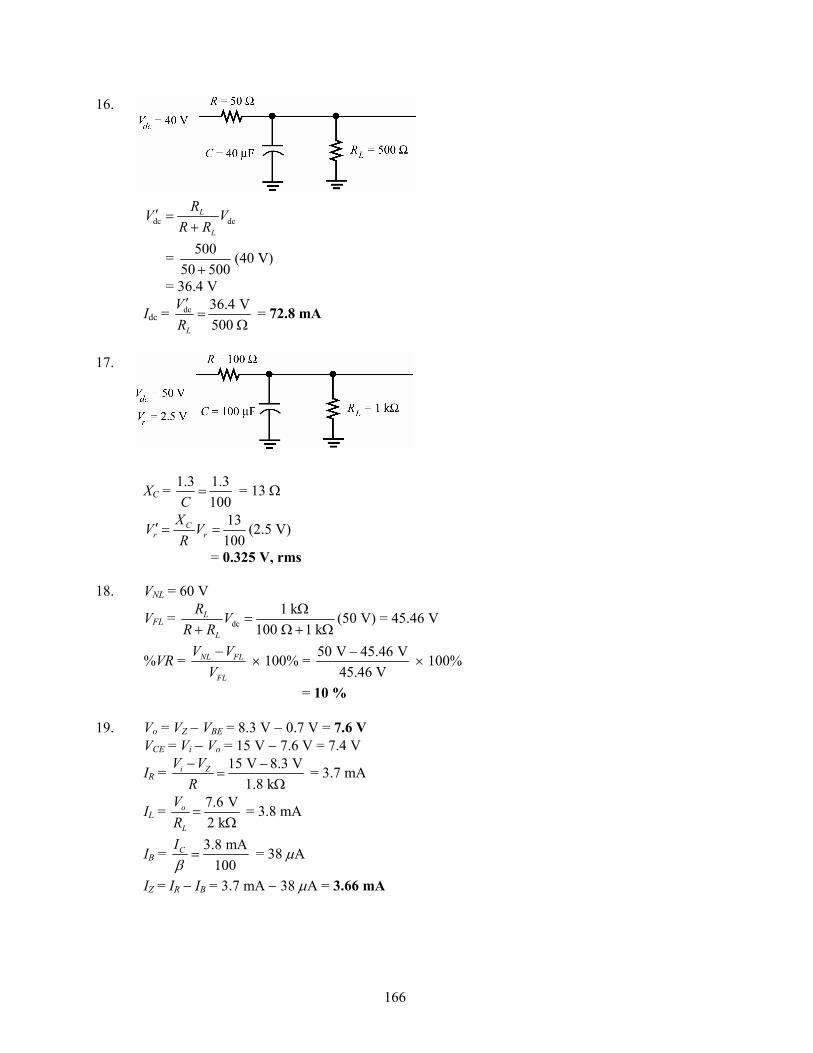
166
16.
dc dcL
L
RV VR R
′ =+
= 50050 500+
(40 V)
= 36.4 V
Idc = dc 36.4 V500 L
VR′=
Ω = 72.8 mA
17.
XC = 1.3 1.3100C
= = 13 Ω
13100
Cr r
XV VR
′ = = (2.5 V)
= 0.325 V, rms 18. VNL = 60 V
VFL = dc1 k
100 1 kL
L
R VR R
Ω=
+ Ω + Ω(50 V) = 45.46 V
%VR = NL FL
FL
V VV− × 100% = 50 V 45.46 V
45.46 V− × 100%
= 10 % 19. Vo = VZ − VBE = 8.3 V − 0.7 V = 7.6 V VCE = Vi − Vo = 15 V − 7.6 V = 7.4 V
IR = 15 V 8.3 V1.8 k
i ZV VR− −
=Ω
= 3.7 mA
IL = 7.6 V2 k
o
L
VR
=Ω
= 3.8 mA
IB = 3.8 mA100
CIβ
= = 38 μA
IZ = IR − IB = 3.7 mA − 38 μA = 3.66 mA
167
20. Vo = 2
1 2
2
( )BEzR R V V
R+
+
= 33 k 22 k22 kΩ+ Ω
Ω(10 V + 0.7 V)
= 26.75 V
21. Vo = 1
2
12 k1 1 10 V8.2 kZ
R VR
⎛ ⎞ Ω⎛ ⎞+ = +⎜ ⎟ ⎜ ⎟Ω⎝ ⎠⎝ ⎠
= 24.6 V 22. Vo = VL = 10 V + 0.7 V = 10.7 V 23. 24. IL = 250 mA Vm = Vr(rms) ⋅ 2 = 2 (20 V) = 28.3 V
peakrV = 3 Vr(rms) = dc2.43 I
C⎛ ⎞⎜ ⎟⎝ ⎠
= 2.4(250)3500
⎛ ⎞⎜ ⎟⎝ ⎠
= 2.1 V
Vdc = Vm − peakrV = 28.3 V − 2.1 V = 26.2 V
Vi(low) = Vdc − peakrV = 26.2 V − 2.1 V = 24.1 V
25. To maintain Vi(min) ≥ 7.3 V (see Table 15.1)
peakrV ≤ Vm − Vi(min) = 12 V − 7.3 V = 4.7 V
so that
Vr(rms) = peak 4.7 V1.733
rV= = 2.7 V
The maximum value of load current is then
Idc = (rms) (2.7 V)(200)2.4 2.4
rV C= = 225 mA
168
26. Vo = Vref2
1
1 RR
⎛ ⎞+⎜ ⎟
⎝ ⎠ + IadjRL
= 1.25 V 1.8 k1240
Ω⎛ ⎞+⎜ ⎟Ω⎝ ⎠ + 100 μA(2.4 kΩ)
= 1.25 V(8.5) + 0.24 V = 10.87 V
27. Vo = Vref2
1
1 RR
⎛ ⎞+⎜ ⎟
⎝ ⎠ + Iadj R2
= 1.25 V 1.5 k1220
Ω⎛ ⎞+⎜ ⎟Ω⎝ ⎠ + 100 μA(1.5 kΩ)
= 9.9 V
169
Chapter 16 1. (a) The Schottky Barrier diode is constructed using an n-type semiconductor material and a
metal contact to form the diode junction, while the conventional p-n junction diode uses both p- and n-type semiconductor materials to form the junction.
(b) − 2. (a) In the forward-biased region the dynamic resistance is about the same as that for a p-n
junction diode. Note that the slope of the curves in the forward-biased region is about the same at different levels of diode current.
(b) In the reverse-biased region the reverse saturation current is larger in magnitude than
for a p-n junction diode, and the Zener breakdown voltage is lower for the Schottky diode than for the conventional p-n junction diode.
3. 100 A 0.5 A 1.33 A/ C75 C
RIC
μ μ μΔ −= = °
Δ° °
(1.33 A/ C) C (1.33 A/ C)(25 C) 33.25 ARI μ μ μΔ = ° Δ = ° ° = 0.5 A+33.25 ARI μ μ= = 33.75 Aμ
4. 1 12 2 (1 MHz)(7 pF)CX
fCπ π= = = 22.7 kΩ
400 mV10 mA
FDC
F
VRI
= = = 40 Ω
5. Temperature on linear scale T(1/2 power level of 100 mW) ≅ 95°C 6. VF a linear scale VF (25°C) ≅ 380 mV = 0.38 V At 125°C, VF ≅ 280 mV
100 mV100 C
F
T
VΔ=
Δ ° = 1 mV/°C
∴ At 100°C VF = 280 mV + (1 mV/°C)(25°C) = 280 mV + 25 mV = 305 mV Increase temperature and VF drops.
170
7. (a) CT(VR) = ( ) 1/ 3
(0) 80 pF4.2 V1 10.7 V
nR T
CV V
=⎛ ⎞+ +⎜ ⎟⎝ ⎠
= 80 pF1.912
= 41.85 pF
(b) k = CT(VT + VR)n = 41.85 pF(0.7 V + 4.2 V)1/3
1.698 ≅ 71 × 10−12 8. (a) At −3 V, C = 40 pF At −12 V, C = 20 pF ΔC = 40 pF − 20 pF = 20 pF
(b) At −8 V, 40 pF20 VR
CVΔ
=Δ
= 2 pF/V
At −2 V, 60 pF9 VR
CVΔ
=Δ
= 6.67 pF/V
R
CVΔΔ
increases at less negative values of VR.
9. Ratio = ( 1 V) 92pF( 8 V) 5.5 pF
t
t
CC
−=
− = 16.73
( 1.25 V)( 7 V)
t
t
CC−−
= 13
10. Ct ≅ 15 pF
1 1
2 2 (10 MHz)(3 )(15 pF) vs on chart
s t
QfR Cπ π
= =Ω
= 354.61 350
11. TCC = 1 0( )o
CC T T
Δ−
× 100% ⇒ T1 = 100%( )C o
CTC CΔ × + To
= (0.11 pF)(100)(0.02)(22 pF)
+ 25
= 50°C 12. VR from −2 V to −8 V Ct(−2 V) = 60 pF, Ct(−8 V) = 6 pF
Ratio = ( 2 V) 60 pF( 8 V) 6 pF
t
t
CC
−=
− = 10
171
13. Q(−1 V) = 82, Q(−10 V) = 5000
Ratio = ( 10 V) 5000Q( 1 V) 82Q −
=−
= 60.98
BW = 610 10 Hz
82of
Q×
= = 121.95 kHz
BW = 610 10 Hz
5000of
Q×
= = 2 kHz
14. High-power diodes have a higher forward voltage drop than low-current devices due to larger
IR drops across the bulk and contact resistances of the diode. The higher voltage drops result in higher power dissipation levels for the diodes, which in turn may require the use of heat sinks to draw the heat away from the body of the structure.
15. The primary difference between the standard p-n junction diode and the tunnel diode is that
the tunnel diode is doped at a level from 100 to several thousand times the doping level of a p-n junction diode, thus producing a diode with a “negative resistance” region in its characteristic curve.
16. At 1 MHz: XC = 6 12
1 12 2 (1 10 Hz)(5 10 F)fCπ π −=
× ×
= 31.83 kΩ
At 100 MHz: XC = 6 12
12 (100 10 Hz)(5 10 F)π −× ×
= 318.3 Ω
At 1 MHz: SLX = 2πfL = 2π(1 × 10⁶ Hz)(6 × 10⁻⁹ H)
= 0.0337 Ω
At 100 MHz: SLX = 2π(100 × 106 Hz)(6 × 10⁻⁹ H)
= 3.769 Ω Ls effect is negligible! R and C in parallel: f = 1 MHz
ZT = (152 180 )(31.83 k 90 )152 31.83 kj
Ω∠ ° Ω∠− °− Ω − Ω
= −152.05 Ω∠0.27° ≅ −152 Ω∠0°
f = 100 MHz
ZT = (152 180 )(318.3 90 )152 318.3j
Ω∠ ° ∠− °− Ω −
= −137.16 Ω∠25.52 ≠ −152 Ω∠0° At very high frequencies XC has some impact!
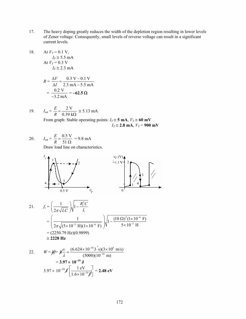
172
17. The heavy doping greatly reduces the width of the depletion region resulting in lower levels of Zener voltage. Consequently, small levels of reverse voltage can result in a significant current levels.
18. At VT = 0.1 V, IF ≅ 5.5 mA At VT = 0.3 V IF ≅ 2.3 mA
R = 0.3 V 0.1 V2.3 mA 5.5 mA
VI
Δ −=
Δ −
= 0.2 V3.2 mA−
= −62.5 Ω
19. Isat = 2 V0.39 k
ER=
Ω ≅ 5.13 mA
From graph: Stable operating points: IT ≅ 5 mA, VT ≅ 60 mV IT ≅ 2.8 mA, VT = 900 mV
20. Isat = 0.5 V51
ER=
Ω = 9.8 mA
Draw load line on characteristics.
21. fs = 21 1
2lR CLLCπ
⎛ ⎞−⎜ ⎟
⎝ ⎠
= 2 6
33 6
1 (10 ) (1 10 F)15 10 H2 (5 10 H)(1 10 F)π
−
−− −
⎛ ⎞ Ω ×⎜ ⎟ −⎜ ⎟ ×× ×⎝ ⎠
= (2250.79 Hz)(0.9899) ≅ 2228 Hz
22. W = hf= 34 8
10
(6.624 10 J s)(3 10 m/s)(5000)(10 m)
vhλ
−
−
× ⋅ ×=
= 3.97 × 10⁻¹⁹ J
3.97 × 10⁻¹⁹ J 19
1 eV1.6 10 J−
⎡ ⎤⎢ ⎥×⎣ ⎦
= 2.48 eV
°
173
23. (a) Visible spectrum: 3750 A → 7500 (b) Silicon, peak relative response ≅ 8400 A (c) BW = 10,300 A − 6100 A = 4200 A
24. 9 2
12
4 10 W/m1.609 10
−
−
××
= 2,486 fc
From the intersection of VA = 30 V and 2,486 fc we find Iλ ≅ 440 μA 25. (a) Silicon
(b) 1 A = 10−10 m, 7
10
6 10 m10 m/A
−
−
× ⇒ 6000 A → orange
26. Note that Vλ is given and not V. At the intersection of Vλ = 25 V and 3000fc we find Iλ ≅ 500 μA and VR = IλR = (500 × 10−6 A)(100 × 103 Ω) = 50 V 27. (a) Extending the curve: 0.1 kΩ → 1000fc, 1 kΩ → 25fc
3(1 0.1) 10
(1000 25)c c
Rf f
Δ − × Ω=
Δ − = 0.92 Ω/fc ≅ 0.9 Ω/fc
(b) 1 kΩ → 25fc, 10 kΩ → 1.3fc
3(10 1) 10
(25 1.3)c c
Rf f
Δ − × Ω=
Δ − = 379.75 Ω/fc ≅ 380 Ω/fc
(c) 10 kΩ → 1.3fc, 100 kΩ → 0.15fc
3(100 10) 10
(1.3 0.15)c c
Rf f
Δ − ×=
Δ − = 78,260.87 Ω/fc ≅ 78 × 103 Ω/fc
The greatest rate of change in resistance occurs in the low illumination region. 28. The “dark current” of a photodiode is the diode current level when no light is striking the
diode. It is essentially the reverse saturation leakage current of the diode, comprised mainly of minority carriers.
29. 10fc → R ≅ 2 kΩ
Vo = 6 V = 3
3 3
(2 10 )2 10 5 10
iV× Ω× Ω + × Ω
Vi = 21 V
°
° ° °
°°°
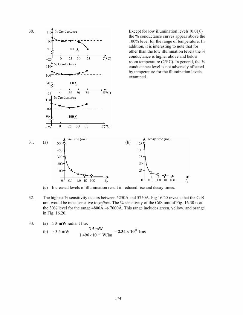
174
30. Except for low illumination levels (0.01fc) the % conductance curves appear above the 100% level for the range of temperature. In addition, it is interesting to note that for other than the low illumination levels the % conductance is higher above and below room temperature (25°C). In general, the % conductance level is not adversely affected by temperature for the illumination levels examined.
31. (a) (b) (c) Increased levels of illumination result in reduced rise and decay times. 32. The highest % sensitivity occurs between 5250A and 5750A. Fig 16.20 reveals that the CdS
unit would be most sensitive to yellow. The % sensitivity of the CdS unit of Fig. 16.30 is at the 30% level for the range 4800A → 7000A. This range includes green, yellow, and orange in Fig. 16.20.
33. (a) ≅ 5 mW radiant flux
(b) ≅ 3.5 mW 13
3.5 mW1.496 10 W/lm−×
= 2.34 × 10¹⁰ lms
°°
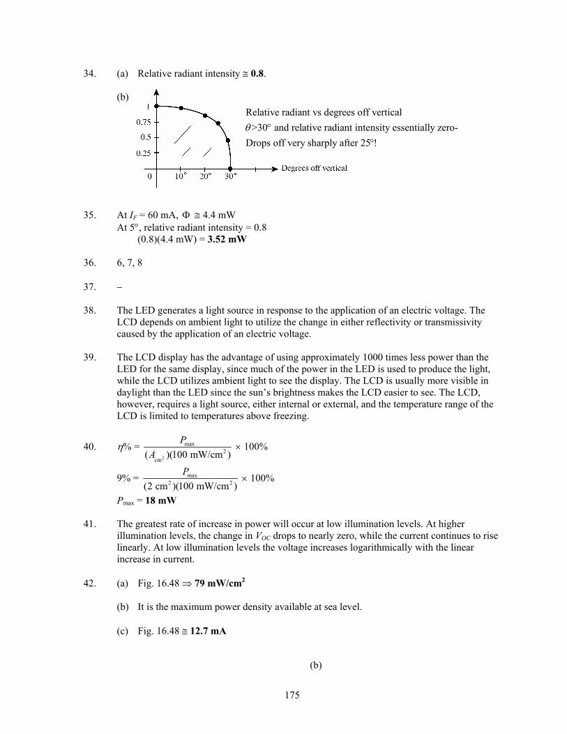
175
34. (a) Relative radiant intensity ≅ 0.8. (b) 35. At IF = 60 mA, Φ ≅ 4.4 mW At 5°, relative radiant intensity = 0.8 (0.8)(4.4 mW) = 3.52 mW 36. 6, 7, 8 37. − 38. The LED generates a light source in response to the application of an electric voltage. The
LCD depends on ambient light to utilize the change in either reflectivity or transmissivity caused by the application of an electric voltage.
39. The LCD display has the advantage of using approximately 1000 times less power than the
LED for the same display, since much of the power in the LED is used to produce the light, while the LCD utilizes ambient light to see the display. The LCD is usually more visible in daylight than the LED since the sun’s brightness makes the LCD easier to see. The LCD, however, requires a light source, either internal or external, and the temperature range of the LCD is limited to temperatures above freezing.
40. η% = 2
max2
cm( )(100 mW/cm )
PA
× 100%
9% = max2 2(2 cm )(100 mW/cm )
P × 100%
Pmax = 18 mW 41. The greatest rate of increase in power will occur at low illumination levels. At higher
illumination levels, the change in VOC drops to nearly zero, while the current continues to rise linearly. At low illumination levels the voltage increases logarithmically with the linear increase in current.
42. (a) Fig. 16.48 ⇒ 79 mW/cm2 (b) It is the maximum power density available at sea level. (c) Fig. 16.48 ≅ 12.7 mA
(b)
Relative radiant vs degrees off vertical>30 and relative radiant intensity essentially zero-
Drops off very sharply after 25 !θ °
°
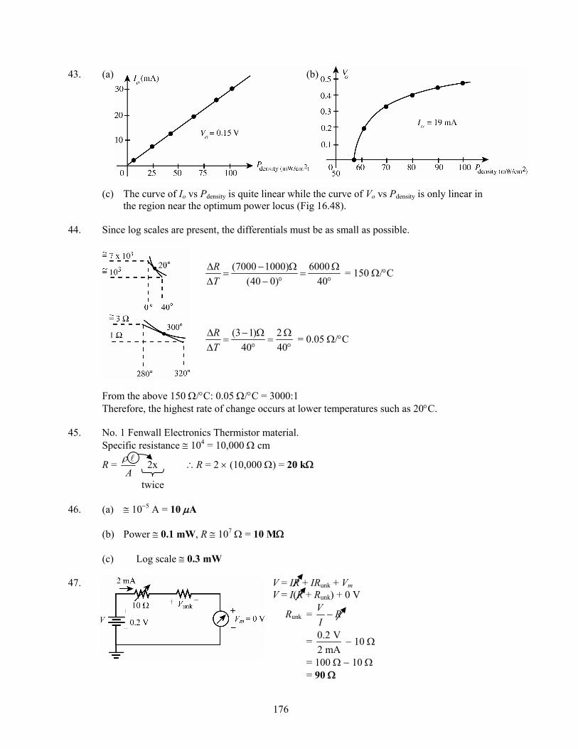
176
43. (a) (b)
(c) The curve of Io vs Pdensity is quite linear while the curve of Vo vs Pdensity is only linear in
the region near the optimum power locus (Fig 16.48). 44. Since log scales are present, the differentials must be as small as possible.
(7000 1000) 6000(40 0) 40
RT
Δ − Ω Ω= =
Δ − ° ° = 150 Ω/°C
(3 1) 240 40
RT
Δ − Ω Ω= =
Δ ° ° = 0.05 Ω/°C
From the above 150 Ω/°C: 0.05 Ω/°C = 3000:1 Therefore, the highest rate of change occurs at lower temperatures such as 20°C. 45. No. 1 Fenwall Electronics Thermistor material. Specific resistance ≅ 104 = 10,000 Ω cm
R = Aρ 2x ∴R = 2 × (10,000 Ω) = 20 kΩ
twice 46. (a) ≅ 10−5 A = 10 μA (b) Power ≅ 0.1 mW, R ≅ 107 Ω = 10 MΩ (c) Log scale ≅ 0.3 mW 47. V = IR + IRunk + Vm V = I(R + Runk) + 0 V
Runk = V RI−
= 0.2 V2 mA
− 10 Ω
= 100 Ω − 10 Ω = 90 Ω
177
Chapter 17 1. − 2. − 3. − 4. (a) p-n junction diode (b) The SCR will not fire once the gate current is reduced to a level that will cause the
forward blocking region to extend beyond the chosen anode-to-cathode voltage. In general, as IG decreases, the blocking voltage required for conduction increases.
(c) The SCR will fire once the anode-to-cathode voltage is less than the forward blocking
region determined by the gate current chosen. (d) The holding current increases with decreasing levels of gate current. 5. (a) Yes (b) No (c) No. As noted in Fig. 17.8b the minimum gate voltage required to trigger all units is 3 V. (d) VG = 6 V, IG = 800 mA is a good choice (center of preferred firing area). VG = 4 V, IG = 1.6 A is less preferable due to higher power dissipation in the gate. Not in
preferred firing area. 6. In the conduction state, the SCR has characteristics very similar to those of a p-n junction
diode (where VT = 0.7 V). 7. The smaller the level of R1, the higher the peak value of the gate current. The higher the peak
value of the gate current the sooner the triggering level will be reached and conduction initiated.
8. (a) VP = sec (rms) 22
V⎛ ⎞⎜ ⎟⎝ ⎠
= ( )117 V 22
= 82.78 V
VDC = 0.636(82.78 V) = 52.65 V (b) VAK = VDC − VBatt = 52.65 V − 11 V = 41.65 V
178
(c) VR = VZ + VGK = 11 V + 3 V = 14 V At 14 V, SCR2 conducts and stops the charging process. (d) At least 3 V to turn on SCR2.
(e) V2 ≅ 12 PV = 1 (82.78 V)
2 = 41.39 V
9. − 10. (a) Charge toward 200 V but will be limited by the development of a negative voltage
VGK ( )1Z CV V= − that will eventually turn the GTO off.
(b) τ = R3C1 = (20 kΩ)(0.1 μF) = 2 ms 5τ = 10 ms
(c) 5τ ′ = 1 (5 )2
τ = 5 ms = 5RGTO C1
RGTO = 61
5 ms 5 ms5 5(0.1 10 F)C −=
× = 10 kΩ 1 (20 k above)
2⎛ ⎞= Ω −⎜ ⎟⎝ ⎠
11. (a) ≅ 0.7 mW/cm2 (b) 0°C → 0.82 mW/cm2 100°C → 0.16 mW/cm2
0.82 0.160.82− × 100% ≅ 80.5%
12. VC = VBR + VGK = 6 V + 3 V = 9 V VC = 40(1 − e−t/RC) = 9 40 − 40e−t/RC = 9 40e−t/RC = 31 e−t/RC = 31/40 = 0.775 RC = (10 × 103 Ω)(0.2 × 10⁻⁶ F) = 2 × 10⁻³ s loge(e−t/RC) = loge 0.775 −t/RC = −t/2 × 10−3 = −0.255 and t = 0.255(2 × 10⁻³) = 0.51 ms 13. − 14.
1 2BR BRV V= ± 10% 2BRV
= 6.4 V ± 0.64 V ⇒ 5.76 V → 7.04 V 15. −
179
16. P
P
V VI− > R1
6
40 V [0.6(40 V) + 0.7 V]10 10−
−×
= 1.53 MΩ > R1
V
V
V VI− < R1 ⇒ 40 V 1 V
8 mA− = 4.875 kΩ < R1
∴1.53 MΩ > R1 > 4.875 kΩ
17. (a) η = 1
1 20E
B
B B I
R
R R=
+ ⇒ 0.65 =
2
2 k2 k BR
ΩΩ+
2BR = 1.08 kΩ
(b) RBB = ( )1 2
0EB B I
R R=
+ = 2 kΩ + 1.08 kΩ = 3.08 kΩ
(c)
1BRV = ηVBB = 0.65(20 V) = 13 V
(d) VP = ηVBB + VD = 13 V + 0.7 V = 13.7 V
18. (a) η = 1
0E
B
BB I
RR
=
0.55 = 1
10 kBRΩ
!BR = 5.5 kΩ
RBB = ! 2B BR R+
10 kΩ = 5.5 kΩ + 2BR
2BR = 4.5 kΩ
(b) VP = ηVBB + VD = (0.55)(20 V) + 0.7 V = 11.7 V
(c) R1 < 20 V 11.7 V50 A
P
p
V VI μ− −
= = 166 kΩ
ok: 68 kΩ < 166 kΩ
180
(d) t1 = R1C logeV
P
V VV V−−
= (68 × 103)(0.1 × 10⁻⁶) loge18.88.3
= 5.56 ms
t2 = 1 2( )BR R+ C loge P
V
VV
= (0.2 kΩ + 2.2 kΩ)(0.1 × 10⁻⁶) loge11.71.2
= 0.546 ms T = t1 + t2 = 6.106 ms
f = 1 16.106 msT
= = 163.77 Hz
(e) (f)
2
2
2
2.2 k (20 V)2.2 k 10 kR
BB
R VVR R
Ω= =
+ Ω + Ω
= 3.61 V
2
1
2
2
( 0.7 V)PR
B
R VVR R
−≅
+
= 2.2 k (11.7 V 0.7 V)2.2 k 0.2 kΩ −
Ω+ Ω
= 10.08 V
(g) f ≅ 1
1 1 log (1/(1 )) (6.8 k )(0.1 F)log 2.22e eR C η μ
=− Ω
= 184.16 Hz
difference in frequency levels is partly due to the fact that t2 ≅ 10% of t1. 19. IB = 25 μA IC =
ef Bh I = (40)(25 μA) = 1 mA
181
20.
21. (a) DF = ITΔΔ
= 0.95 0 0.9525 ( 50) 75
−=
− − = 1.26%/°C
(b) Yes, curve flattens after 25°C. 22. (a) At 25°C, ICEO ≅ 2 nA At 50°C, ICEO ≅ 30 nA
9(30 2) 10 A 28 nA
(50 25) C 25 CCEOIT
−Δ − ×= =
Δ − ° ° = 1.12 nA/°C
ICEO (35°C) = ICEO(25°C) + (1.12 nA/°C)(35°C − 25°C) = 2 nA + 11.2 nA = 13.2 nA From Fig. 17.55 ICEO (35°C) ≅ 4 nA Derating factors, therefore, cannot be defined for large regions of non-linear curves.
Although the curve of Fig. 17.55 appears to be linear, the fact that the vertical axis is a log scale reveals that ICEO and T( °C) have a non-linear relationship.
23. 20 mA45 mA
o C
i F
I II I= =
≅ = 0.44
Yes, relatively efficient.
182
24. (a) PD = VCEIC = 200 mW
IC = max
200 mW30 V
D
CE
PV
= = 6.67 mA @ VCE = 30 V
VCE = 200 mW10 mA
D
C
PI
= = 20 V @ IC = 10 mA
IC = 200 mW25 V
D
CE
PV
= = 8.0 mA @ VCE = 25 V
Almost the entire area of Fig. 17.57 falls within the power limits.
(b) βdc = 4 mA10 mA
C
F
II
= = 0.4, Fig. 17.56 C
F
II
≅ 4 mA10 mA
= 0.4
The fact that the IF characteristics of Fig. 17.57 are fairly horizontal reveals that the level
of IC is somewhat unaffected by the level of VCE except for very low or high values. Therefore, a plot of IC vs. IF as shown in Fig. 17.56 can be provided without any reference to the value of VCE. As noted above, the results are essentially the same.
25. (a) IC ≥ 3 mA (b) At IC = 6 mA; RL = 1 kΩ, t = 8.6 μs RL = 100 Ω; t = 2 μs 1 kΩ:100 Ω = 10:1 8.6 μs:2 μs = 4.3:1 ΔR:Δt ≅ 2.3:1
26. η = 2
2 2
3 33 4
B
B B
RR R
=+
= 0.75, VG = ηVBB = 0.75(20 V) = 15 V
27. VP = 8.7 V, IP = 100 μA ZP = 8.7 V100 A
P
P
VI μ
= = 87 kΩ (≅ open)
VV = 1 V, IV = 5.5 mA ZV = 1 V5.5 mA
V
V
VI
= = 181.8 Ω (relatively low)
87 kΩ: 181.8 Ω = 478.55:1 ≅ 500:1
183
28. Eq. 17.23: T = RC loge log( )
BB BBe
BB P BB BB D
V VRCV V V V Vη⎛ ⎞ ⎛ ⎞
=⎜ ⎟ ⎜ ⎟− − +⎝ ⎠ ⎝ ⎠
Assuming ηVBB VD, T = RC loge (1 )BB
BB
VV η⎛ ⎞⎜ ⎟−⎝ ⎠
= RC loge(1/1− η) = RC loge1
1 2
1
1 B
B B
RR R
⎛ ⎞⎜ ⎟⎜ ⎟⎜ ⎟−⎜ ⎟⎜ ⎟+⎝ ⎠
= RC loge1 2 1
2 2
log 1B B Be
B B
R R RRC
R R⎛ ⎞ ⎛ ⎞+
= +⎜ ⎟ ⎜ ⎟⎜ ⎟ ⎜ ⎟⎝ ⎠ ⎝ ⎠
Eq. 17.24
29. (a) Minimum VBB:
Rmax = BB P
P
V VI− ≥ 20 kΩ
( )BB BB D
P
V V VIη− + = 20 kΩ
VBB − ηVBB − VD = IP 20 kΩ VBB(1 − η) = IP 20 kΩ + VD
VBB = 20 k1
P DI VηΩ +−
= (100 A)(20 k ) 0.7 V1 0.67
μ Ω +−
= 8.18 V 10 V OK
(b) R < 12 V 1 V5.5 mA
BB V
V
V VI− −
= = 2 kΩ
R < 2 kΩ
(c) T ≅ RC loge1
2
1 B
B
RR
⎛ ⎞+⎜ ⎟⎜ ⎟
⎝ ⎠
2 × 10−3 = R(1 × 10⁻⁶)loge10 k15 k
Ω⎛ ⎞+⎜ ⎟Ω⎝ ⎠
loge3 = 1.0986
R = 3
6
2 10(1 10 )(1.0986)
−
−
××
R = 1.82 kΩ

Solutions for Laboratory Manual to accompany
Electronic Devices and Circuit Theory
Tenth Edition
Prepared by Franz J. Monssen
185

186
EXPERIMENT 1: OSCILLOSCOPE AND FUNCTION GENERATOR OPERATIONS Part 1: The Oscilloscope
a. it focuses the beam on the screen b. adjusts the brightness of the beam on the screen c. allows the moving of trace in either screen direction d. selects volts/screen division on y-axis e. selects unit of time/screen division on x-axis g. allows for ac or dc coupling of signal to scope and at GND position; establishes ground reference on screen h. locates the trace if it is off screen i. provide for the adjustment of scope from external reference source k. determines mode of triggering of the sweep voltage m. the input impedance of many scopes consists of the parallel combination of a 1 Meg resistance and a 30pf capacitor n. measuring device which reduces loading of scope on a circuit and effectively increases input impedance of scope by a factor of 10.
Part 2: The Function Generator
d. T = l/f = 1/1000 Hz = l ms e. (calculated): 1 ms*[l cm/.2 ms] = 5cm (measured): 5 cm = same f. (calculated): l ms*[cm/.5ms] =2 cm (measured): 2 cm = same g. (calculated): 1 ms*[cm/1ms] = l cm (measured): l cm = same h. .2 ms/cm takes 5 boxes to display total wave .5 ms/cm takes 2 boxes to display total wave 1 ms/cm takes 1 box to display total wave i. 1. adjust timebase to obtain one cycle of the wave 2. count the number of cm's occupied by the wave 3. note the timebase setting 4. multiply timebase setting by number of cm's occupied by wave. This is equal to the period of the wave. 5. obtain its reciprocal; that's the frequency.
187
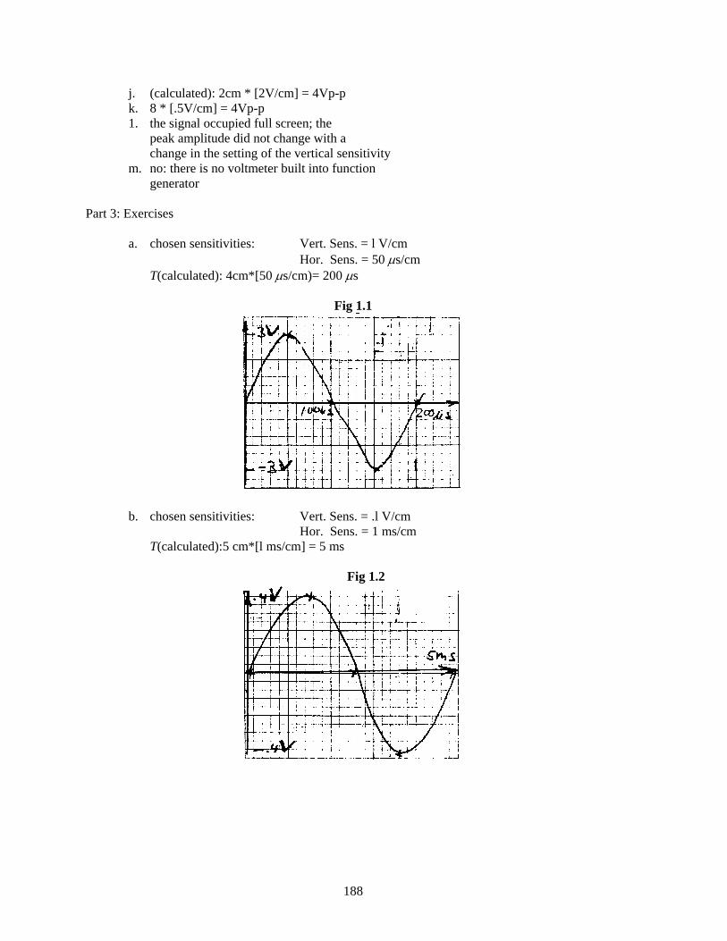
j. (calculated): 2cm * [2V/cm] = 4Vp-p k. 8 * [.5V/cm] = 4Vp-p 1. the signal occupied full screen; the
peak amplitude did not change with a change in the setting of the vertical sensitivity
m. no: there is no voltmeter built into function generator
Part 3: Exercises a. chosen sensitivities: Vert. Sens. = l V/cm
Hor. Sens. = 50 μs/cm T(calculated): 4cm*[50 μs/cm)= 200 μs
Fig 1.1
b. chosen sensitivities: Vert. Sens. = .l V/cm
Hor. Sens. = 1 ms/cm T(calculated):5 cm*[l ms/cm] = 5 ms
Fig 1.2
188
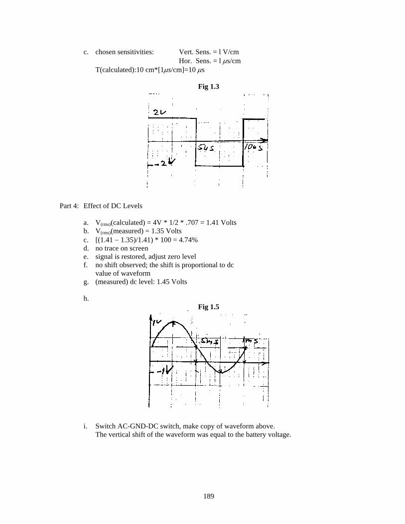
c. chosen sensitivities: Vert. Sens. = l V/cm Hor. Sens. = l μs/cm
T(calculated):10 cm*[1μs/cm]=10 μs
Fig 1.3
Part 4: Effect of DC Levels
a. V(rms)(calculated) = 4V * 1/2 * .707 = 1.41 Volts b. V(rms)(measured) = 1.35 Volts c. [(1.41 − 1.35)/1.41) * 100 = 4.74% d. no trace on screen e. signal is restored, adjust zero level f. no shift observed; the shift is proportional to dc value of waveform g. (measured) dc level: 1.45 Volts h.
Fig 1.5
i. Switch AC-GND-DC switch, make copy of waveform above.
The vertical shift of the waveform was equal to the battery voltage.
189
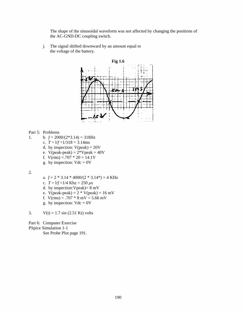
The shape of the sinusoidal waveform was not affected by changing the positions of the AC-GND-DC coupling switch.
j. The signal shifted downward by an amount equal to the voltage of the battery.
Fig 1.6
Part 5: Problems 1. b. f = 2000/(2*3.14) = 318Hz c. T = l/f =1/318 = 3.14ms d. by inspection: V(peak) = 20V e. V(peak-peak) = 2*Vpeak = 40V f. V(rms) =.707 * 20 = 14.1V g. by inspection: Vdc = 0V 2. a. f = 2 * 3.14 * 4000/(2 * 3.14*) = 4 KHz c. T = l/f =1/4 Khz = 250 μs d. by inspection:Vpeak)= 8 mV e. V(peak-peak) = 2 * V(peak) = 16 mV f. V(rms) = .707 * 8 mV = 5.66 mV g. by inspection: Vdc = 0V 3. V(t) = 1.7 sin (2.51 Kt) volts Part 6: Computer Exercise PSpice Simulation 1-1 See Probe Plot page 191.
190
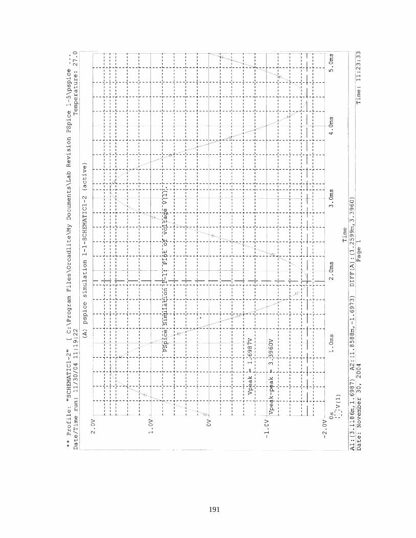
191
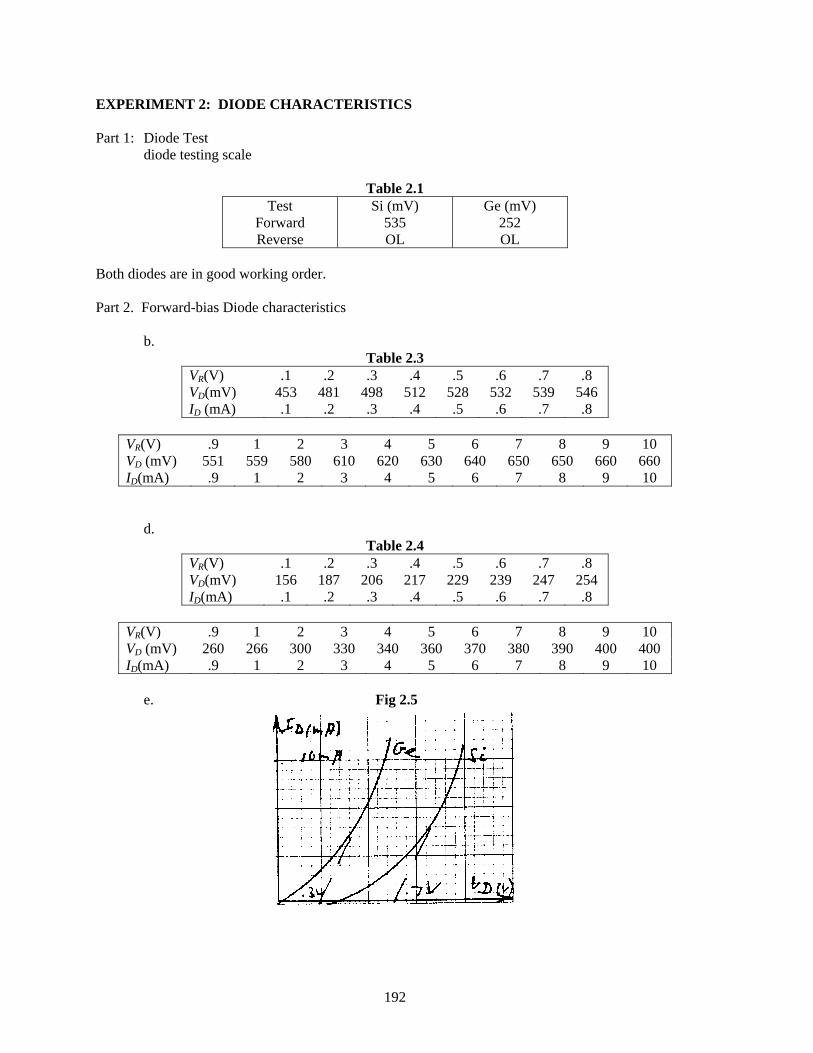
EXPERIMENT 2: DIODE CHARACTERISTICS Part 1: Diode Test diode testing scale
Table 2.1 Test
Forward Reverse
Si (mV) 535 OL
Ge (mV) 252 OL
Both diodes are in good working order. Part 2. Forward-bias Diode characteristics b.
Table 2.3 VR(V) VD(mV) ID (mA)
.1 453 .1
.2 481 .2
.3 498 .3
.4 512 .4
.5 528 .5
.6 532 .6
.7 539 .7
.8 546 .8
VR(V) .9 1 2 3 4 5 6 7 8 9 10 VD (mV) 551 559 580 610 620 630 640 650 650 660 660 ID(mA) .9 1 2 3 4 5 6 7 8 9 10
d.
Table 2.4 VR(V) VD(mV) ID(mA)
.1 156 .1
.2 187 .2
.3 206 .3
.4 217 .4
.5 229 .5
.6 239 .6
.7 247 .7
.8 254 .8
VR(V) .9 1 2 3 4 5 6 7 8 9 10 VD (mV) 260 266 300 330 340 360 370 380 390 400 400 ID(mA) .9 1 2 3 4 5 6 7 8 9 10
e. Fig 2.5
192
f. Their shapes are similar, but for a given ID, the potential VD is greater for the silicon diode compared to the germanium diode. Also, the Si has a higher firing potential than the germanium diode.
Part 3: Reverse Bias b. Rm = 9.9 Mohms VR(measured) = 9.1 mV IS(calculated) = 8.21 nA c. VR(measured) = 5.07 mV IS(calculated) = 4.58 μA d. The IS level of the germanium diode is approximately 500 times as large as that of the silicon diode. e. RDC (Si) = 2.44*109 ohms RDC(Ge) = 3.28 M*106 ohms These values are effective open-circuits when compared to resistors in the kilohm range. Part 4: DC Resistance a.
Table 2.5 ID (mA) VD (mV) RDC (ohms)
.2 350 1750 1.0 559 559 5.0 630 126
10.0 660 66 b.
Table 2.6 ID (mA) VD (mV) RDC (ohms)
.2 80 400 1.0 180 180 5.0 340 68
10.0 400 40 Part 5: AC Resistance a. (calculated)rac = 3.4 ohms b. (calculated)rac = 2.9 ohms c. (calculated)rac = 27.0 ohms d. (calculated)rac = 26.0 ohms Part 6: Firing Potential VT(silicon) = 540 mV VT(germanium) = 260 mV
193
Part 7: Temperature Effects c. For an increase in temperature, the forward diode current will increase while the voltage
VD across the diode will decline. Since RD = VD/ID, therefore, the resistance of a diode declines with increasing temperature.
d. As the temperature across a diode increases, so does the current. Therefore, relative to the
diode current, the diode has a positive temperature coefficient. Part 9: Computer Exercises PSpice Simulation 2-1 1. See Probe plot page 195. 2. RD 600mV = 658 Ω RD 700 mV = 105 Ω 4. RD 600 mV = 257 Ω 5. See Probe Plot V(D1) versus I(D1) 7. Silicon 8. See Probe plot page 196. 9. See Probe plot page 196. 10. See Probe plot page 196.
194
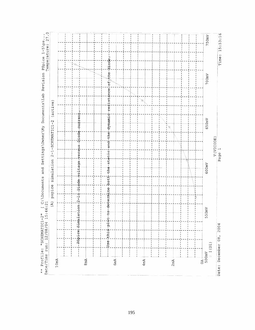
195
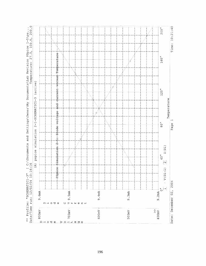
196
EXPERIMENT 3: SERIES AND PARALLEL DIODE CONFIGURATIONS Part 1: Threshold Voltage VT Fig 3.2 Firing voltage: Silicon: 595 mV Germanium: 310 mV Part 2: Series Configuration
b. VD = .59 V VO (calculated) = 5 − .595 = 4.41 V ID = 4.41/2.2 K = 2 mA c. VD(measured) = .59 V VO(measured) = 4.4 V ID(from measured) = 2 mA e. VD = 595 mV VO(calculated) = (5 − .595) 1 K/(1 K + 2.2 K) = 1.33 V ID = 1.36 mA f. VD = .57 V VO = 1.36 V ID(from measured) = 1.36 V/1 K = 1.36 mA g. VD(measured) = 5 V h. VD(measured) = 5 V VO(measured) = 0 V VO(measured) = 0 V ID(measured) = 0 A ID(measured) = 0 A j. V1(calculated) = .905 V VO(calculated) = 4.1 V ID(calculated) = 1.86 mA
Part 7: Computer Exercise PSpice Simulation 3-2 1. 638.0 mV
197
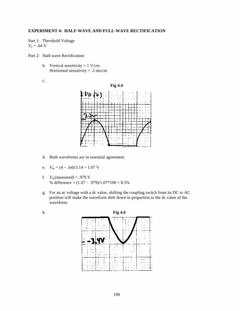
EXPERIMENT 4: HALF-WAVE AND FULL-WAVE RECTIFICATION Part 1: Threshold Voltage VT = .64 V Part 2: Half-wave Rectification b. Vertical sensitivity = 1 V/cm Horizontal sensitivity = .2 ms/cm c.
Fig 4.4
d. Both waveforms are in essential agreement. e. Vdc = (4 − .64)/3.14 = 1.07 V f. Vdc(measured) = .979 V % difference = (1.07 − .979)/1.07*100 = 8.5% g. For an ac voltage with a dc value, shifting the coupling switch from its DC to AC
position will make the waveform shift down in proportion to the dc value of the waveform.
h. Fig 4.6
198
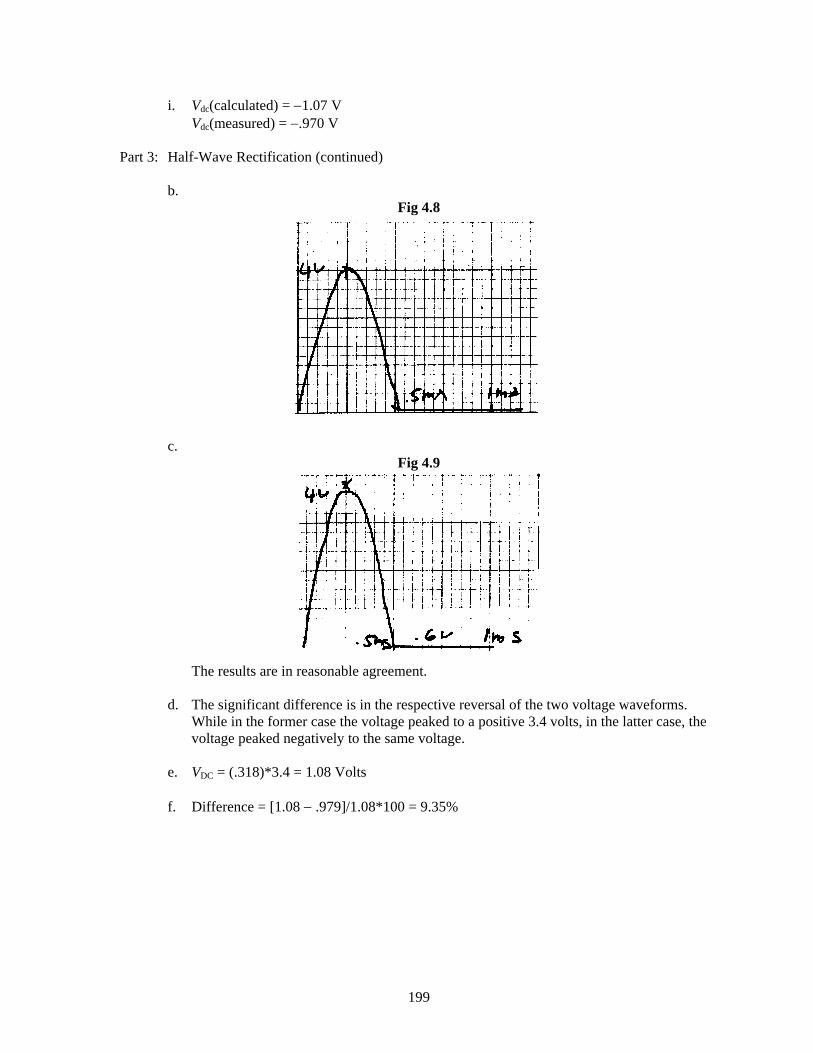
i. Vdc(calculated) = −1.07 V Vdc(measured) = −.970 V Part 3: Half-Wave Rectification (continued) b.
Fig 4.8
c.
Fig 4.9
The results are in reasonable agreement. d. The significant difference is in the respective reversal of the two voltage waveforms.
While in the former case the voltage peaked to a positive 3.4 volts, in the latter case, the voltage peaked negatively to the same voltage.
e. VDC = (.318)*3.4 = 1.08 Volts f. Difference = [1.08 − .979]/1.08*100 = 9.35%
199
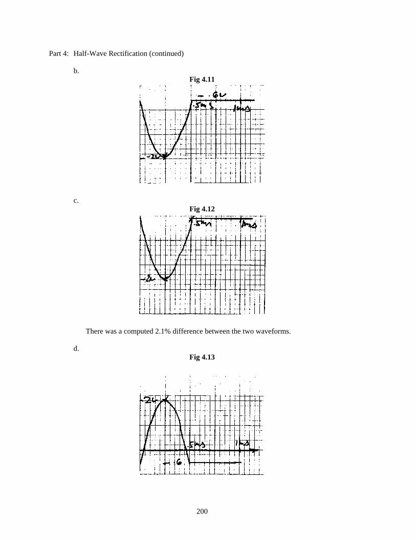
Part 4: Half-Wave Rectification (continued) b.
Fig 4.11
c.
Fig 4.12
There was a computed 2.1% difference between the two waveforms. d.
Fig 4.13
200
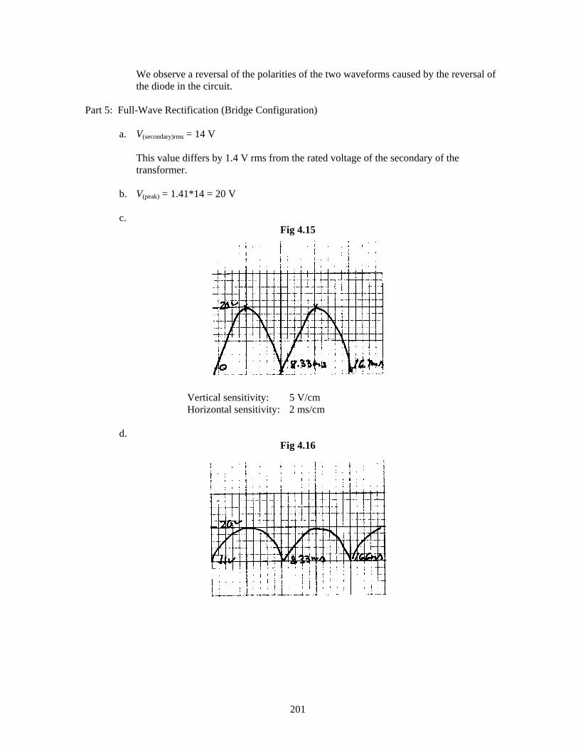
We observe a reversal of the polarities of the two waveforms caused by the reversal of the diode in the circuit.
Part 5: Full-Wave Rectification (Bridge Configuration) a. V(secondary)rms = 14 V This value differs by 1.4 V rms from the rated voltage of the secondary of the
transformer. b. V(peak) = 1.41*14 = 20 V c.
Fig 4.15
Vertical sensitivity: 5 V/cm Horizontal sensitivity: 2 ms/cm d.
Fig 4.16
201
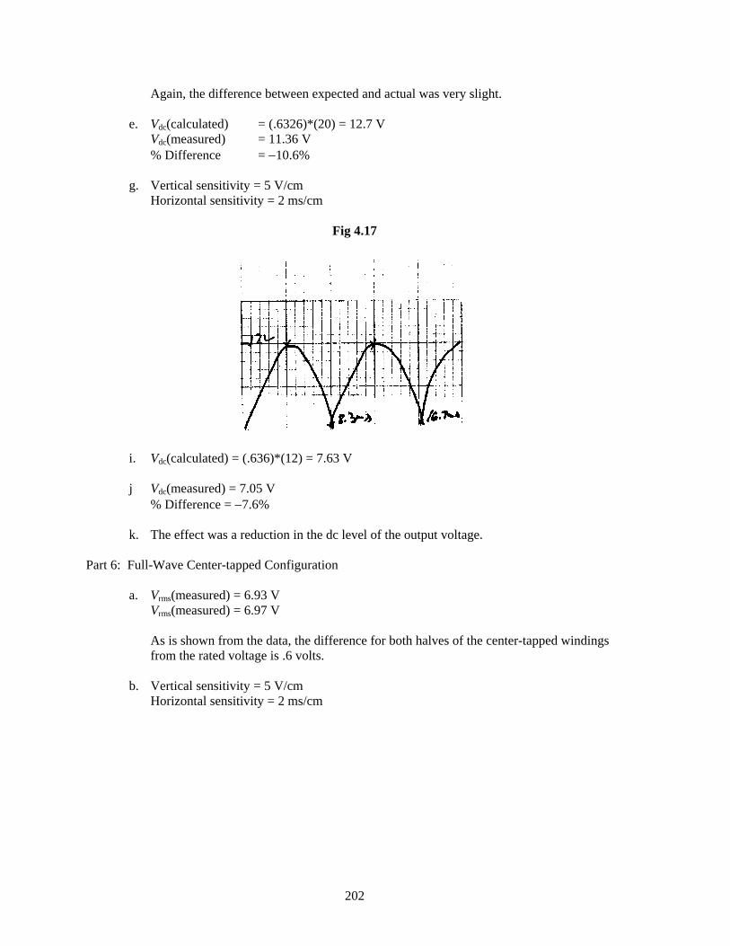
Again, the difference between expected and actual was very slight. e. Vdc(calculated) = (.6326)*(20) = 12.7 V Vdc(measured) = 11.36 V % Difference = −10.6% g. Vertical sensitivity = 5 V/cm Horizontal sensitivity = 2 ms/cm
Fig 4.17
i. Vdc(calculated) = (.636)*(12) = 7.63 V j Vdc(measured) = 7.05 V % Difference = −7.6% k. The effect was a reduction in the dc level of the output voltage. Part 6: Full-Wave Center-tapped Configuration a. Vrms(measured) = 6.93 V Vrms(measured) = 6.97 V As is shown from the data, the difference for both halves of the center-tapped windings
from the rated voltage is .6 volts. b. Vertical sensitivity = 5 V/cm Horizontal sensitivity = 2 ms/cm
202
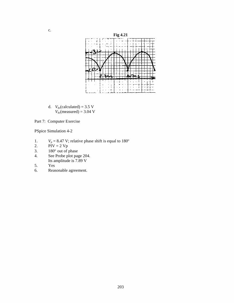
c. Fig 4.21
d. Vdc(calculated) = 3.5 V Vdc(measured) = 3.04 V Part 7: Computer Exercise PSpice Simulation 4-2 1. Vp = 8.47 V; relative phase shift is equal to 180° 2. PIV = 2 Vp 3. 180° out of phase 4. See Probe plot page 204. Its amplitude is 7.89 V 5. Yes 6. Reasonable agreement.
203
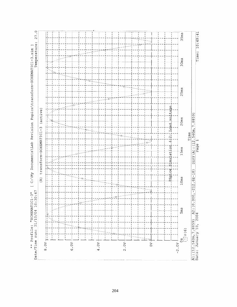
204
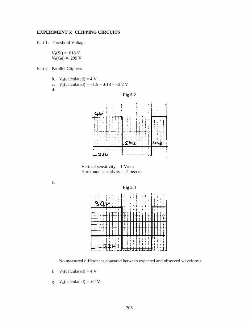
EXPERIMENT 5: CLIPPING CIRCUITS Part 1: Threshold Voltage VT(Si) = .618 V VT(Ge) = .299 V Part 2 Parallel Clippers b. VO(calculated) = 4 V c. VO(calculated) = −1.5 − .618 = −2.2 V d.
Fig 5.2
Vertical sensitivity = 1 V/cm Horizontal sensitivity = .2 ms/cm e.
Fig 5.3
No measured differences appeared between expected and observed waveforms. f. VO(calculated) = 4 V g. VO(calculated) = .62 V
205
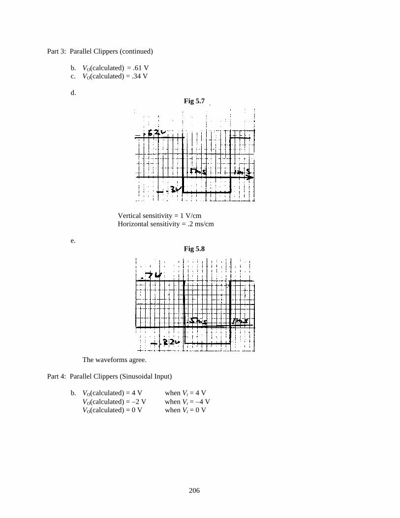
Part 3: Parallel Clippers (continued) b. VO(calculated) = .61 V c. VO(calculated) = .34 V d.
Fig 5.7
Vertical sensitivity = 1 V/cm Horizontal sensitivity = .2 ms/cm e.
Fig 5.8
The waveforms agree. Part 4: Parallel Clippers (Sinusoidal Input) b. VO(calculated) = 4 V when Vi = 4 V VO(calculated) = −2 V when Vi = −4 V VO(calculated) = 0 V when Vi = 0 V
206
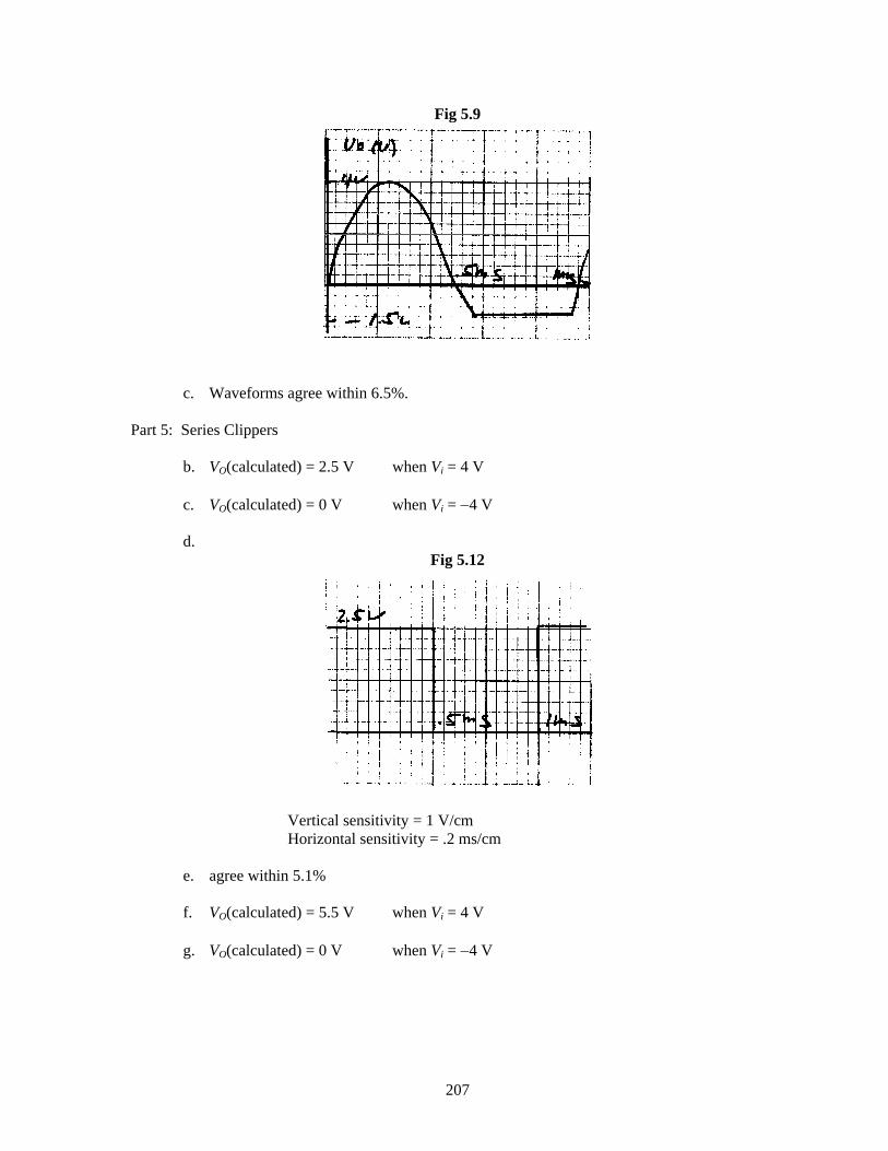
Fig 5.9
c. Waveforms agree within 6.5%. Part 5: Series Clippers b. VO(calculated) = 2.5 V when Vi = 4 V c. VO(calculated) = 0 V when Vi = −4 V d.
Fig 5.12
Vertical sensitivity = 1 V/cm Horizontal sensitivity = .2 ms/cm e. agree within 5.1% f. VO(calculated) = 5.5 V when Vi = 4 V g. VO(calculated) = 0 V when Vi = −4 V
207
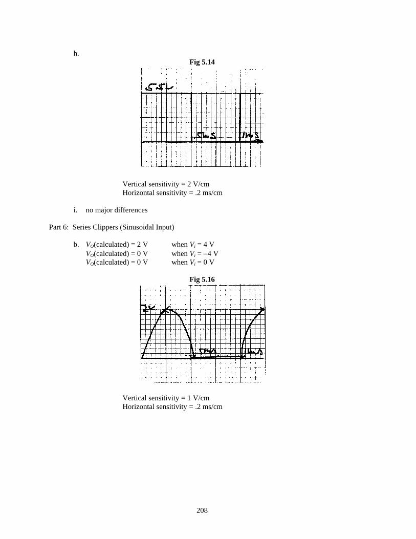
h. Fig 5.14
Vertical sensitivity = 2 V/cm Horizontal sensitivity = .2 ms/cm i. no major differences Part 6: Series Clippers (Sinusoidal Input) b. VO(calculated) = 2 V when Vi = 4 V VO(calculated) = 0 V when Vi = −4 V VO(calculated) = 0 V when Vi = 0 V
Fig 5.16
Vertical sensitivity = 1 V/cm Horizontal sensitivity = .2 ms/cm
208
Part 7: Computer Exercises PSpice Simulation 5-2 1. See Probe plot page 210. 2. VOUT = 4 V 3. No 4. VOUT = −2.067 V 5. Yes, VOUT(ideal) = −1.5 V 6. Reasonable agreement 7. No significant discrepancies 8. See Probe plot page 211. PSpice Simulation 5-3 1. See Probe plot page 212.
2. In close agreement
3. No
4. For V1 = 4 V; Vout = V1 − VD1 − 1.5 V = 4 V − .6 − 1.5 V = 1.9 V For V1 = −4 V; I(D1) = 0 A, ∴ Vout = 0 V
5. See Probe plot page 213.
6. See Probe plot page 213.
7. See Probe plot page 213.
8. See Probe plot page 213.
9. Forward bias voltage of about 600 mV when “ON”. Reverse diode voltage of diode is −4 V − 1.5 V = −5.5 V
209
210
211
212
213
EXPERIMENT 6: CLAMPING CIRCUITS Part 1: Threshold Voltage VT = .62 V Part 2: Clampers (R, C, Diode Combination) b. VC(calculated) = 4 − 0.62 = 3.38 V VO(calculated) = 0.62 V c. VO(calculated) = −4 − 3.38 V = −7.38 V d. Fig 6.2 Vertical sensitivity = 1 V/cm Horizontal sensitivity = .2 ms/cm
214
e. Fig 6.3 f. VC(calculated) = −3.38 V VO(calculated) = −0.62 V g. VO(calculated) = 7.38 V h. Fig 6.4 i. Fig 6.5 Vertical sensitivity = 1 V/cm Horizontal sensitivity = .2 ms/cm
215
Part 3: Clampers with a DC battery b. VC(calculated) = 1.88 V VO(calculated) = 0.62 V + 1.5 V = 2.12 V c. VO(calculated) = −1.88 V − 4 V = −5.88 V d. Fig 6.7
Vertical sensitivity = 1 V/cm Horizontal sensitivity = .2 ms/cm
e. Fig 6.8 f. VC(calculated) = 4.88 V VO(calculated) = 1.5 V − 0.62 V = 0.88 V g. VO(calculated) = 4 V + 4.88 V = 8.88 V
216
h. Fig 6.9
Vertical sensitivity = 2 V/cm Horizontal sensitivity = .2 ms/cm
Part 4: Clampers (Sinusoidal Input) b. VO(calculated) = 0 V when Vi = 2 V VO(calculated) = −2 V when Vi = −3.6 V VO(calculated) = −1.6 V when Vi = 0 V Fig 6.11 Vertical sensitivity = 1 V/cm Horizontal sensitivity = .2 ms/cm
217
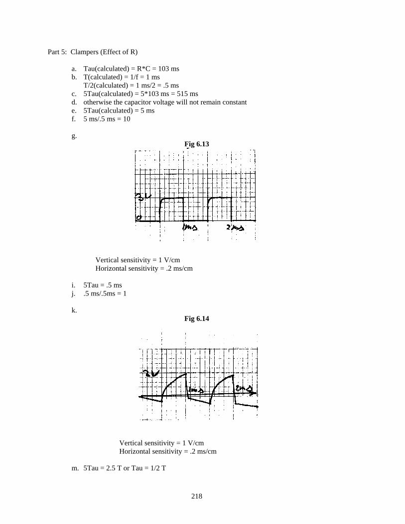
Part 5: Clampers (Effect of R) a. Tau(calculated) = R*C = 103 ms b. T(calculated) = 1/f = 1 ms T/2(calculated) = 1 ms/2 = .5 ms c. 5Tau(calculated) = 5*103 ms = 515 ms d. otherwise the capacitor voltage will not remain constant e. 5Tau(calculated) = 5 ms f. 5 ms/.5 ms = 10 g.
Fig 6.13
Vertical sensitivity = 1 V/cm Horizontal sensitivity = .2 ms/cm i. 5Tau = .5 ms j. .5 ms/.5ms = 1 k.
Fig 6.14
Vertical sensitivity = 1 V/cm Horizontal sensitivity = .2 ms/cm m. 5Tau = 2.5 T or Tau = 1/2 T
218
Part 6: Computer Exercise PSpice Simulation 6-2 1. See Probe Plot page 220. 2. They are the same. 3. VO(calculated) is close to V(2) of Probe plot. 4. See Probe plot page 221. 5. V(1, 2) remains at 2 V during the cycle of V(1) 6. It rises exponentially toward its final value of 2 V. 7. See Probe plot page 222.
219
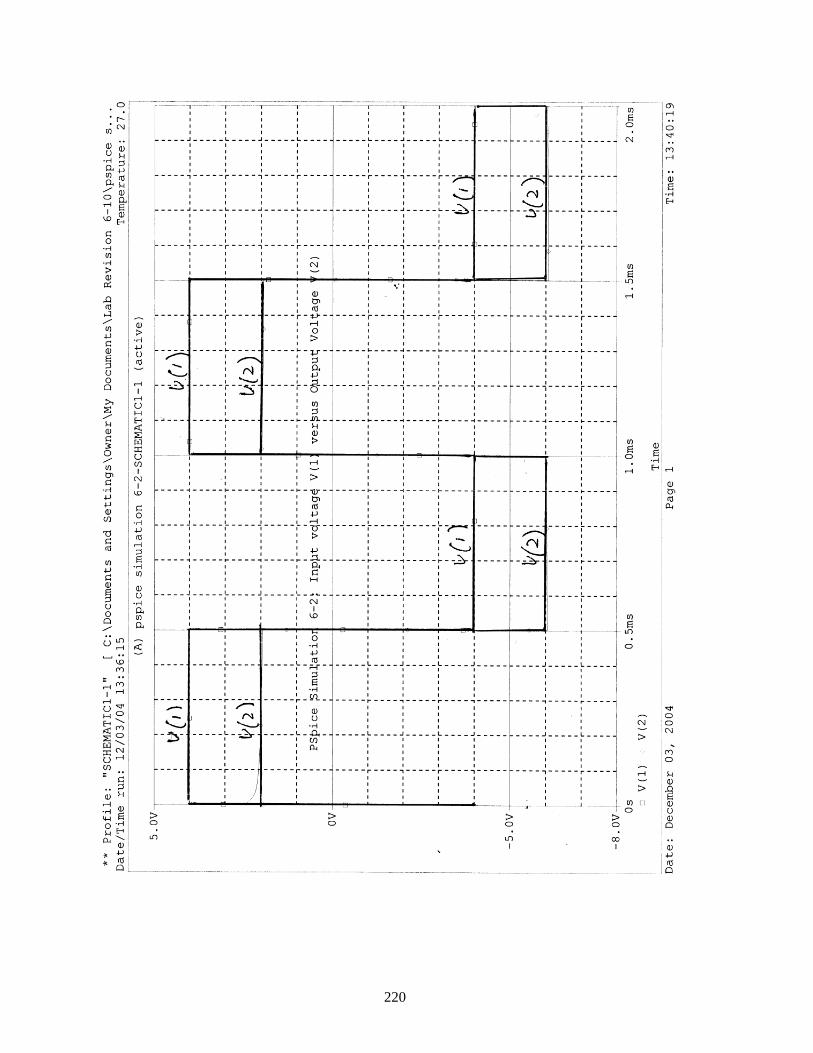
220
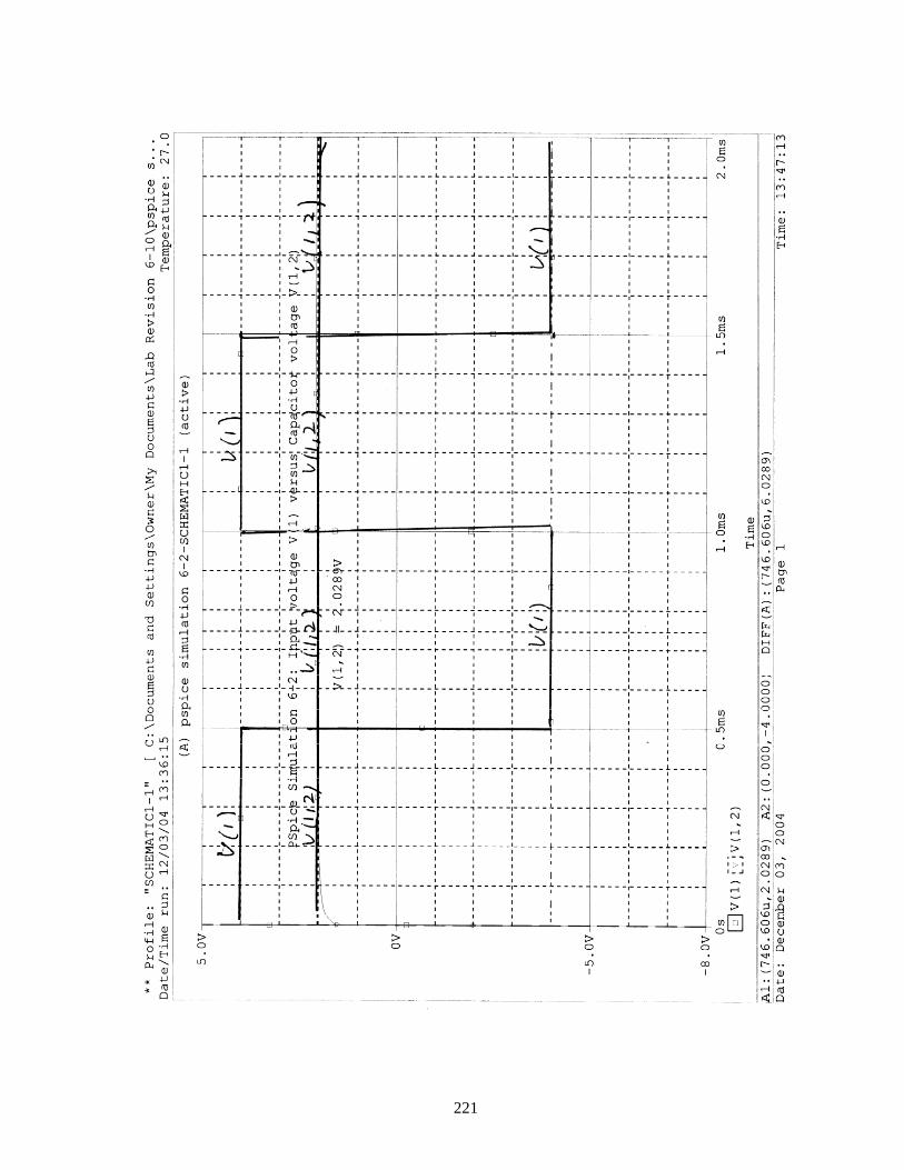
221
222
EXPERIMENT 7: LIGHT-EMITTING AND ZENER DIODES Part 1: LED Characteristics b. VD(measured) = 1.6 V VR(measured) = 49.1 mV ID(calculated) = 49.1 mV/101.4 ohms = 484 μA c. VD(measured) = 1.9 V VR(measured) = 1.55 V ID(calculated) = 1.55 V/101.4 ohms = 15.3 mA d.
E(v) 0 1 2 3 4 5 6 VD (V) 0 1 1.71 1.84 1.93 2.01 2.08 VR (V) 0 0 .34 1.2 2.2 3.1 3.9 ID = VR/R (mA) 0 0 3.3 11.8 21.4 30.6 38.5
e. Fig 7.2
h. The reversed biased Si diode prevents any current from flowing through the circuit,
hence, the LED will not light. k. VR(V) = 3.48 V, therefore ID(mA) = 1.6 mA and LED is in the “good brightness” region. Part 2: Zener Diode Characteristics b. and c.
Table 7.2 E (V) 0 1 2 3 4 5 6 7 8 9 10 11 12 13 14 15 VZ (V) 0 1 2 3 4 5 6 7 8 9 10 10 10.1 10.2 10.3 10.4VR (V) 0 0 0 0 0 0 0 0 0 .1 .97 1.9 2.8 3.7 4.6 4.6IZ (mA) 0 0 0 0 0 0 0 0 0 .99 9.6 18.7 27.6 36.5 45.4 45.4
223
d. Fig 7.5
e. VZ(V) (approximated) = (10.4 + 9)/2 = 9.7 V f. rav(ohms) = (10.4 − 9)/(.045 − .0099) = 39.9 ohms g. RZ(ohms) = 39.9 ohms VZ(V) = 9.7 V Part 3: Zener Diode Regulation a. R (meas) = 979 ohms RL (meas) = 986 ohms VZ (V) = 10.2 V b. VL (V) = 986*15/(979 + 986) = 7.53 V VR (V) = 979*15/(979 + 986) = 7.47 V IR (mA) = 7.47/979 = 7.64 mA IL (mA) = 7.53/986 = 7.63 mA IZ (mA) = IR − IL = 10 μA c. VL (measured) = 7.5 V VR (measured) 7.49 V IR (calculated) = 7.65 mA IL (calculated) = 7.60 mA IZ (calculated) = 50 μA d. VL (calculated) = 11.5 V VR (calculated) 3.54 V IR (calculated) = 3.62 mA IL (calculated) = 3.48 mA IZ (calculated) = .14 mA
224
e. VL (measured) = 9.82 V VR (measured) = 3.54 V IR (calculated) = 3.54 mA IL (calculated) = 2.98 mA IZ (calculated) = .56 mA The difference is expressed as a percent with calculated value as the standard of
reference. percent change of: VL = −14.6% VR = 0.% IR = −2.21% IL = −14.4% IZ = 30.0% f. Rmin/(Rmin + 979)*15 = 9.82 V RL(calculated) = 1.86 Kohms g. Since 2.2 Kohms > Rmin = 1.86 Kohms, therefore, diode is in the “on” state. Part 4: LED-Zener diode combination b. VD = 1.86 V ID = 15.8 mA VZ = 10.07 V Vab(calculated) = 11.9 V c. VL (calculated) = 11.9 V IL (calculated) = 5.41 mA e. E (calculated) = VR + VL = 6.93 + 11.9 = 18.9 V f. E (measured) = 19.1 V The two values are in agreement within 1.06% using E (calculated) as reference.
225
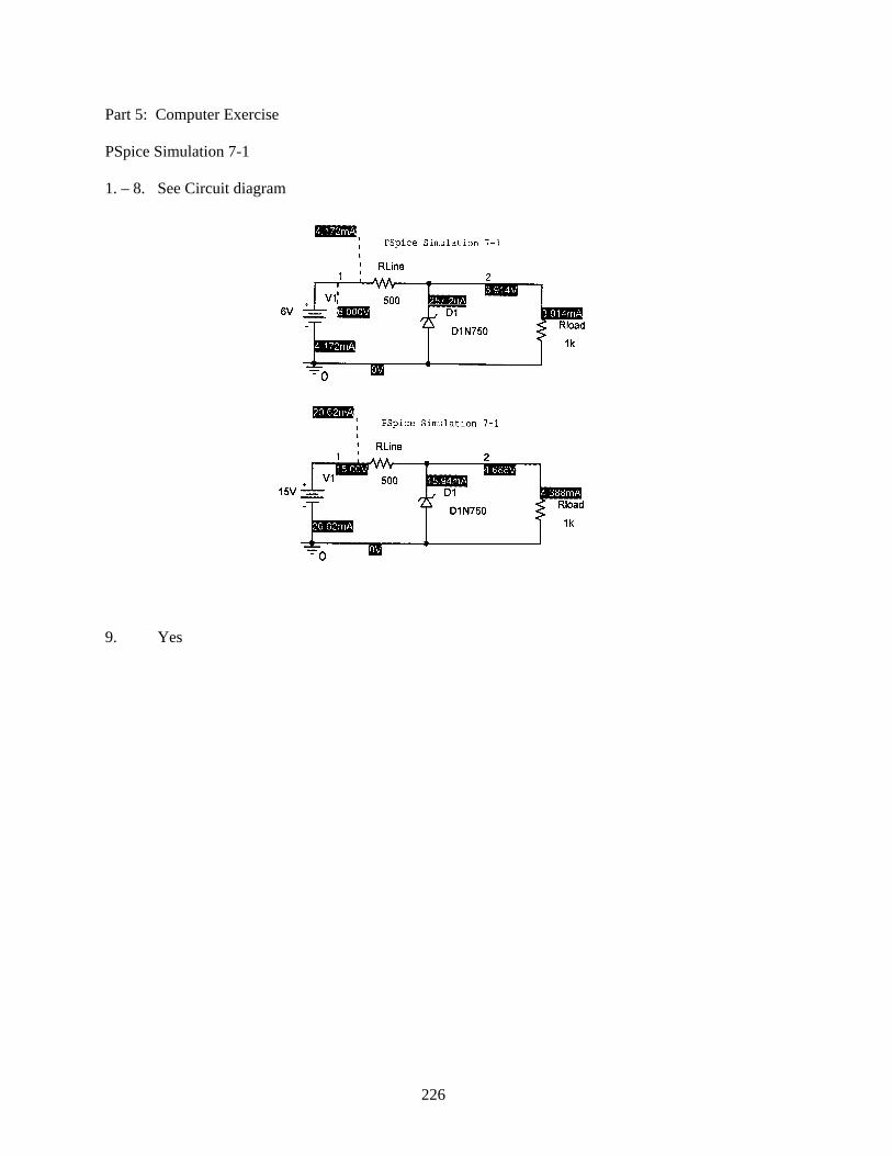
Part 5: Computer Exercise PSpice Simulation 7-1 1. – 8. See Circuit diagram
9. Yes
226
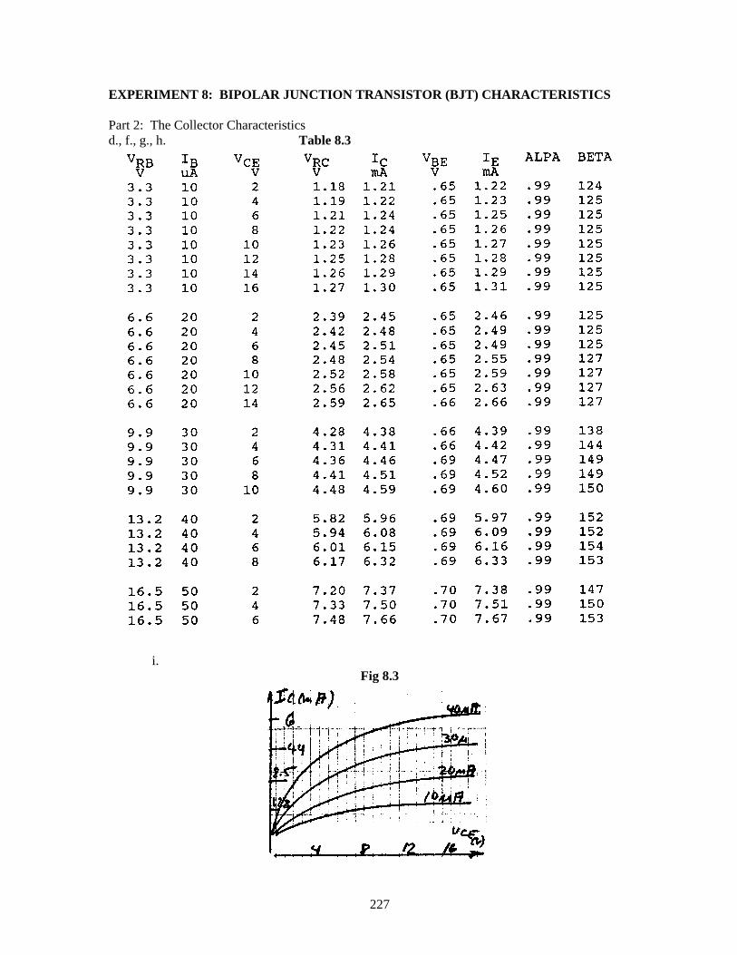
EXPERIMENT 8: BIPOLAR JUNCTION TRANSISTOR (BJT) CHARACTERISTICS Part 2: The Collector Characteristics d., f., g., h. Table 8.3
i.
Fig 8.3
227
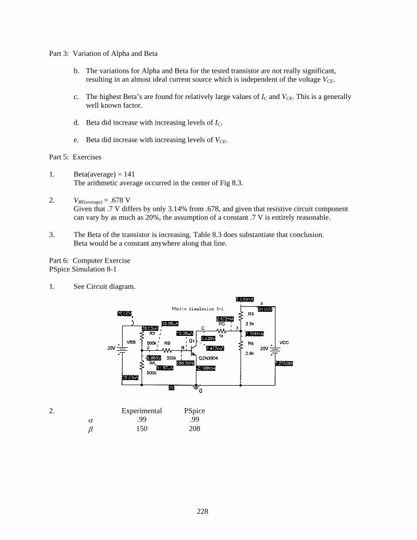
Part 3: Variation of Alpha and Beta
b. The variations for Alpha and Beta for the tested transistor are not really significant, resulting in an almost ideal current source which is independent of the voltage VCE.
c. The highest Beta’s are found for relatively large values of IC and VCE. This is a generally
well known factor. d. Beta did increase with increasing levels of IC. e. Beta did increase with increasing levels of VCE. Part 5: Exercises 1. Beta(average) = 141 The arithmetic average occurred in the center of Fig 8.3. 2. VBE(average) = .678 V Given that .7 V differs by only 3.14% from .678, and given that resistive circuit component
can vary by as much as 20%, the assumption of a constant .7 V is entirely reasonable. 3. The Beta of the transistor is increasing. Table 8.3 does substantiate that conclusion. Beta would be a constant anywhere along that line. Part 6: Computer Exercise PSpice Simulation 8-1 1. See Circuit diagram.
2. Experimental PSpice α .99 .99 β 150 208
228
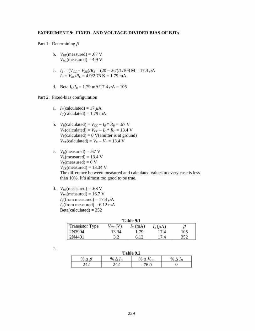
EXPERIMENT 9: FIXED- AND VOLTAGE-DIVIDER BIAS OF BJTs Part 1: Determining β
b. VBE(measured) = .67 V VRC(measured) = 4.9 V c. IB = (VB CC − VBE)/RBB = (20 − .67)/1.108 M = 17.4 μA IC = VRC/RC = 4.9/2.73 K = 1.79 mA d. Beta IC/IB = 1.79 mA/17.4 μA = 105 B
Part 2: Fixed-bias configuration
a. IB(calculated) = 17 μA B
IC(calculated) = 1.79 mA b. VB(calculated) = VB CC − IB * RBB = .67 V VC(calculated) = VCC − IC * RC = 13.4 V VE(calculated) = 0 V(emitter is at ground) VCE(calculated) = VC − VE = 13.4 V c. VB(measured) = .67 V B
VC(measured) = 13.4 V VE(measured) = 0 V VCE(measured) = 13.34 V The difference between measured and calculated values in every case is less than 10%. It’s almost too good to be true. d. VBE(measured) = .68 V VRC(measured) = 16.7 V IB(from measured) = 17.4 μA B
IC(from measured) = 6.12 mA Beta(calculated) = 352
Table 9.1
Transistor Type VCE (V) IC (mA) IB (μA) β 2N3904 13.34 1.79 17.4 105 2N4401 3.2 6.12 17.4 352
e.
Table 9.2 % Δ β % Δ IC % Δ VCE % Δ IBB
242 242 −76.0 0
229
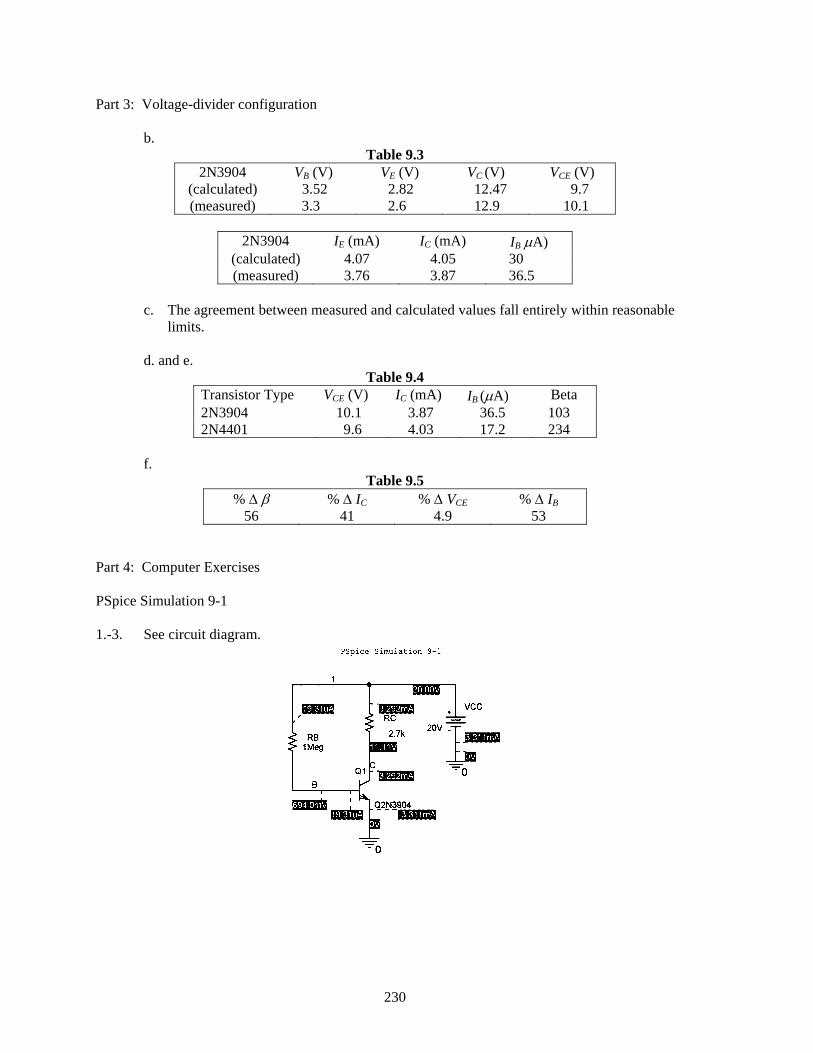
Part 3: Voltage-divider configuration
b. Table 9.3
2N3904 VB (V) B VE (V) VC (V) VCE (V) (calculated) 3.52 2.82 12.47 9.7 (measured) 3.3 2.6 12.9 10.1
2N3904 IE (mA) IC (mA) IB μA) B
(calculated) 4.07 4.05 30 (measured) 3.76 3.87 36.5
c. The agreement between measured and calculated values fall entirely within reasonable
limits. d. and e.
Table 9.4 Transistor Type VCE (V) IC (mA) IB (μA) Beta 2N3904 10.1 3.87 36.5 103 2N4401 9.6 4.03 17.2 234
f.
Table 9.5 % Δ β % Δ IC % Δ VCE % Δ IBB
56 41 4.9 53
Part 4: Computer Exercises PSpice Simulation 9-1 1.-3. See circuit diagram.
230
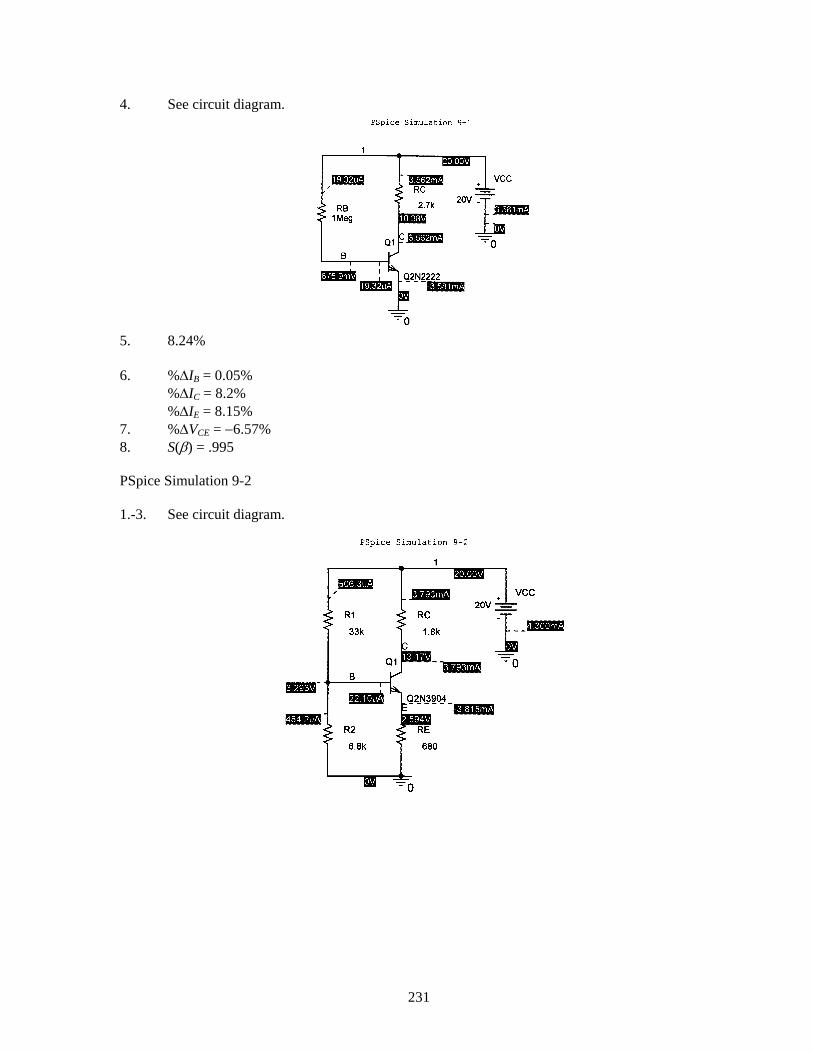
4. See circuit diagram.
5. 8.24% 6. %ΔIB = 0.05% B
%ΔIC = 8.2% %ΔIE = 8.15% 7. %ΔVCE = −6.57% 8. S(β) = .995 PSpice Simulation 9-2 1.-3. See circuit diagram.
231
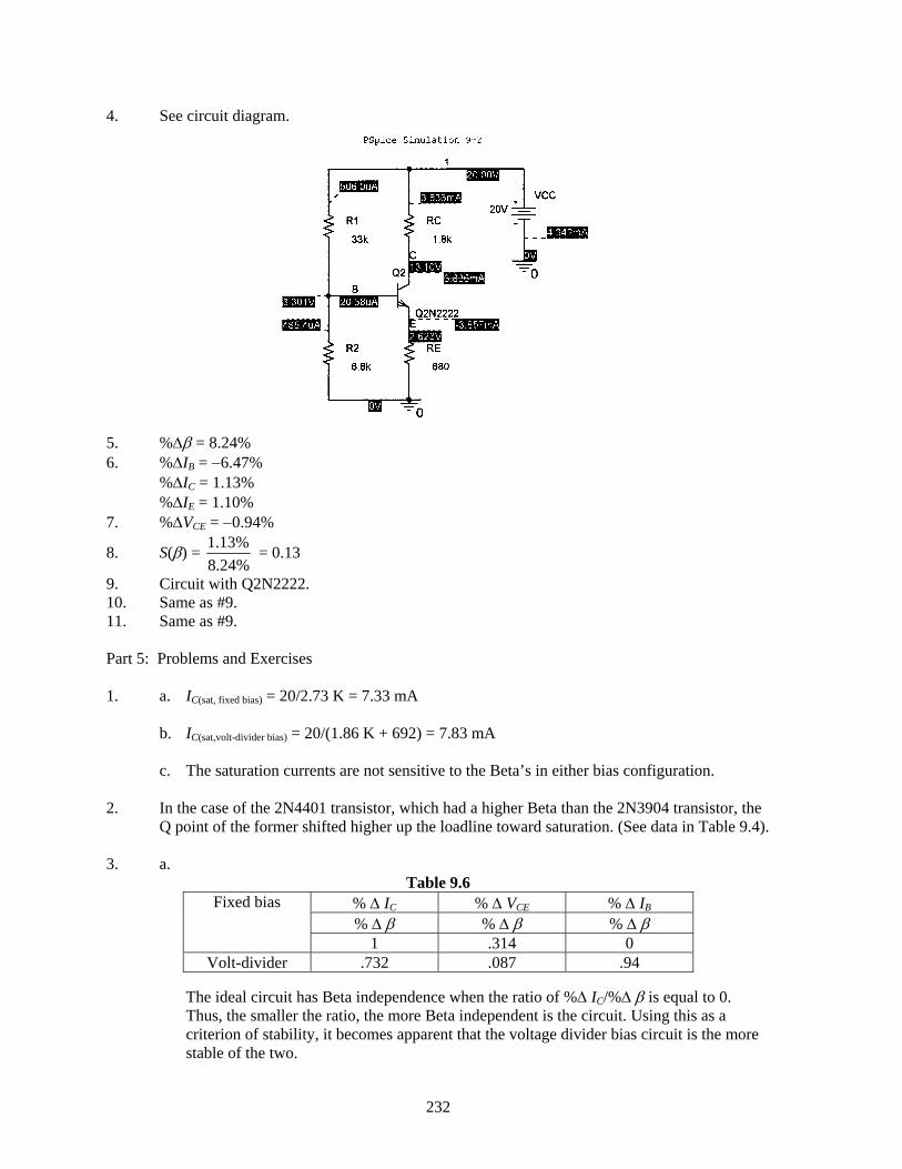
4. See circuit diagram.
5. %Δβ = 8.24% 6. %ΔIB = −6.47% B
%ΔIC = 1.13% %ΔIE = 1.10% 7. %ΔVCE = −0.94%
8. S(β) = 1.13%8.24%
= 0.13
9. Circuit with Q2N2222. 10. Same as #9. 11. Same as #9. Part 5: Problems and Exercises 1. a. IC(sat, fixed bias) = 20/2.73 K = 7.33 mA b. IC(sat,volt-divider bias) = 20/(1.86 K + 692) = 7.83 mA c. The saturation currents are not sensitive to the Beta’s in either bias configuration. 2. In the case of the 2N4401 transistor, which had a higher Beta than the 2N3904 transistor, the
Q point of the former shifted higher up the loadline toward saturation. (See data in Table 9.4). 3. a.
Table 9.6 Fixed bias % Δ IC % Δ VCE % Δ IBB
% Δ β % Δ β % Δ β 1 .314 0
Volt-divider .732 .087 .94
The ideal circuit has Beta independence when the ratio of %Δ IC/%Δ β is equal to 0. Thus, the smaller the ratio, the more Beta independent is the circuit. Using this as a criterion of stability, it becomes apparent that the voltage divider bias circuit is the more stable of the two.
232
4. a. IC = β(VCC − .67)/RB mA B
b. IC = [R2/(R1 + R2)*VCC − .7]/[(R1 || R2)/β + RE] mA c. In equation 4a, the Beta factor cannot be eliminated by a judicious choice of circuit
components. In 4b however, if the quantity R1 || R2/β is made much smaller than RE, then IC is no longer dependent upon Beta. In particular:
IC = [R2/(R1 + R2)*VCC − .7]/RE mA In that case, we have achieved Beta independent biasing.
233
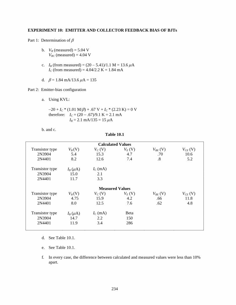
EXPERIMENT 10: EMITTER AND COLLECTOR FEEDBACK BIAS OF BJTs Part 1: Determination of β b. VB (measured) = 5.04 V B
VRC (measured) = 4.04 V c. IB (from measured) = (20 − 5.41)/1.1 M = 13.6 μA B
IC (from measured) = 4.04/2.2 K = 1.84 mA d. β = 1.84 mA/13.6 μA = 135 Part 2: Emitter-bias configuration a. Using KVL: −20 + IC * (1.01 M/β) + .67 V + IC * (2.23 K) = 0 V therefore: IC = (20 − .67)/9.1 K = 2.1 mA IB = 2.1 mA/135 = 15 μA B
b. and c.
Table 10.1
Calculated Values Transistor type VB (V) VC (V) VE (V) VBE (V) VCE (V)
2N3904 5.4 15.3 4.7 .70 10.6 2N4401 8.2 12.6 7.4 .8 5.2
Transistor type IB (μA) B
IC (mA) 2N3904 15.0 2.1 2N4401 11.7 3.3
Measured Values Transistor type VB (V) VC (V) VE (V) VBE (V) VCE (V)
2N3904 4.75 15.9 4.2 .66 11.8 2N4401 8.0 12.5 7.6 .62 4.8
Transistor type IB (μA) B
IC (mA) Beta 2N3904 14.7 2.2 150 2N4401 11.9 3.4 286
d. See Table 10.1. e. See Table 10.1. f. In every case, the difference between calculated and measured values were less than 10%
apart.
234
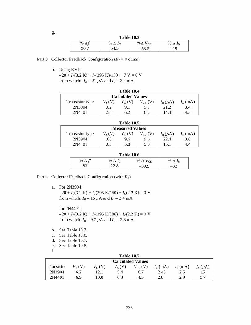
g. Table 10.3
% Δβ % Δ IC %Δ VCE % Δ IBB
90.7 54.5 −58.5 −19 Part 3: Collector Feedback Configuration (RE = 0 ohms) b. Using KVL: −20 + IC(3.2 K) + IC(395 K)/150 + .7 V = 0 V from which: IB = 21 μA and IB C = 3.4 mA
Table 10.4 Calculated Values
Transistor type VB (V) VC (V) VCE (V) IB (μA) B
IC (mA) 2N3904 .62 9.1 9.1 21.2 3.4 2N4401 .55 6.2 6.2 14.4 4.3
Table 10.5
Measured Values Transistor type VB (V) VC (V) VCE (V) IB (μA) B
IC (mA) 2N3904 .68 9.6 9.6 22.4 3.6 2N4401 .63 5.8 5.8 15.1 4.4
Table 10.6
% Δ β % Δ IC % Δ VCE % Δ IBB
83 22.8 −39.9 −33 Part 4: Collector Feedback Configuration (with RE) a. For 2N3904: −20 + IC(3.2 K) + IC(395 K/150) + IC(2.2 K) = 0 V from which: IB = 15 μA and IB C = 2.4 mA for 2N4401: −20 + IC(3.2 K) + IC(395 K/286) + IC(2.2 K) = 0 V from which: IB = 9.7 μA and IB C = 2.8 mA b. See Table 10.7. c. See Table 10.8. d. See Table 10.7. e. See Table 10.8. f.
Table 10.7 Calculated Values
Transistor VB (V) B VC (V) VE (V) VCE (V) IC (mA) IE (mA) IB (μA) B
2N3904 6.2 12.1 5.4 6.7 2.45 2.5 15 2N4401 6.9 10.8 6.3 4.5 2.8 2.9 9.7
235
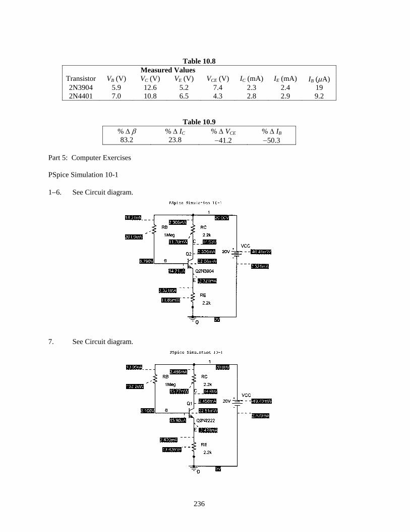
Table 10.8
Measured Values Transistor VB (V) B VC (V) VE (V) VCE (V) IC (mA) IE (mA) IB (μA) B
2N3904 5.9 12.6 5.2 7.4 2.3 2.4 19 2N4401 7.0 10.8 6.5 4.3 2.8 2.9 9.2
Table 10.9 % Δ β % Δ IC % Δ VCE % Δ IBB
83.2 23.8 −41.2 −50.3 Part 5: Computer Exercises PSpice Simulation 10-1 1−6. See Circuit diagram.
7. See Circuit diagram.
236
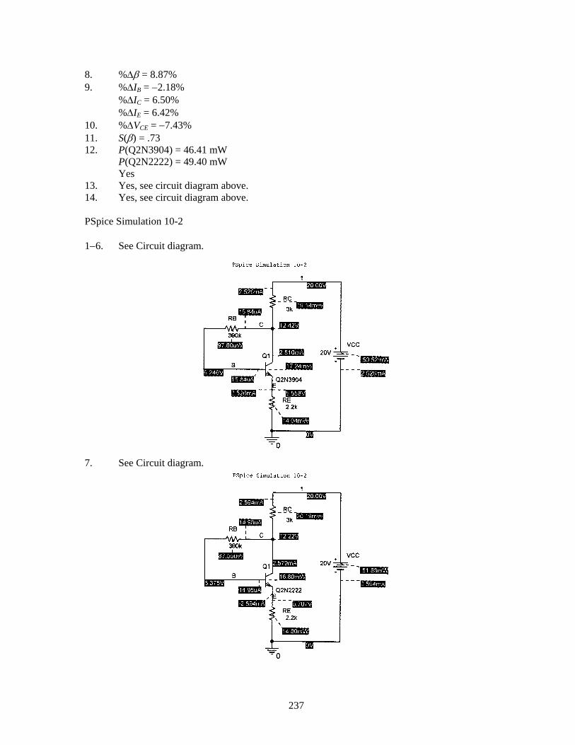
8. %Δβ = 8.87% 9. %ΔIB = −2.18% B
%ΔIC = 6.50% %ΔIE = 6.42% 10. %ΔVCE = −7.43% 11. S(β) = .73 12. P(Q2N3904) = 46.41 mW P(Q2N2222) = 49.40 mW Yes 13. Yes, see circuit diagram above. 14. Yes, see circuit diagram above. PSpice Simulation 10-2 1−6. See Circuit diagram.
7. See Circuit diagram.
237
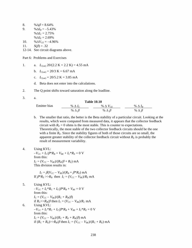
8. %Δβ = 8.64% 9. %ΔIB = −5.43% B
%ΔIC = 2.75% %ΔIE = 2.69% 10. %ΔVCE = −4.96% 11. S(β) = .32 12-14. See circuit diagrams above. Part 6: Problems and Exercises 1. a. IC(sat) 20/(2.2 K + 2.2 K) = 4.55 mA
b. IC(sat) = 20/3 K = 6.67 mA
c. IC(sat) = 20/5.2 K = 3.85 mA
d. Beta does not enter into the calculations. 2. The Q point shifts toward saturation along the loadline. 3. a.
Table 10.10 Emitter bias % Δ IC % Δ VCE % Δ IBB
% Δ β % Δ β % Δ β b. The smaller that ratio, the better is the Beta stability of a particular circuit. Looking at the
results, which were computed from measured data, it appears that the collector feedback circuit with RE = 0 ohms is the most stable. This is counter to expectations. Theoretically, the most stable of the two collector feedback circuits should be the one with a finite RE. Since the stability figures of both of those circuits are so small, the apparent greater stability of the collector feedback circuit without RE is probably the result of measurement variability.
4. Using KVL: −VCC + IC/β*RB + VB BE + IC*RE = 0 V from this: IC = (VCC − VBE)/(RB/β + RB E) mA This division results in: IC = β(VCC − VBE)/(RB + β*RB E) mA If β*RE >>RB then IB C = (VCC − VBE)/RE mA 5. Using KVL: −VCC + IC*RC + IC/β*RB + VB BE = 0 V from this: IC = (VCC − VBE)/(RC + RB/β) B
if RC>>RB/β then IB C = (VCC − VBE)/RC mA 6. Using KVL: −VCC + IC*RC + IC/β*RB + VB BE + IC*RE = 0 V from this: IC = (VCC − VBE)/(RC + RE + RB/β) mA B
if (RC + RE)>>RB/β then IB C = (VCC − VBE)/(RC + RE) mA
238
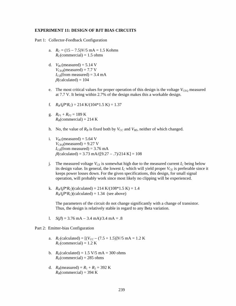
EXPERIMENT 11: DESIGN OF BJT BIAS CIRCUITS Part 1: Collector-Feedback Configuration a. RC = (15 − 7.5)V/5 mA = 1.5 Kohms RC(commercial) = 1.5 ohms d. VRC(measured) = 5.14 V VCEQ(measured) = 7.7 V ICQ(from measured) = 3.4 mA β(calculated) = 104 e. The most critical values for proper operation of this design is the voltage VCEQ measured
at 7.7 V. It being within 2.7% of the design makes this a workable design. f. RB/(β*RB C) = 214 K/(104*1.5 K) = 1.37 g. RF1 + RF2 = 189 K RB(commercial) + 214 K B
h. No, the value of RB is fixed both by VB CC and VBE, neither of which changed. i. VRC(measured) = 5.64 V VCEQ(measured) = 9.27 V ICQ(from measured) = 3.76 mA β(calculated) = 3.73 mA/([9.27 − .7)/214 K] = 108 j. The measured voltage VCE is somewhat high due to the measured current IC being below
its design value. In general, the lowest IC which will yield proper VCE is preferable since it keeps power losses down. For the given specifications, this design, for small signal operation, will probably work since most likely no clipping will be experienced.
k. RB/(β*RB C)(calculated) = 214 K/(108*1.5 K) = 1.4 RB/(β*RB C)(calculated) = 1.34 (see above) The parameters of the circuit do not change significantly with a change of transistor. Thus, the design is relatively stable in regard to any Beta variation. l. S(β) = 3.76 mA − 3.4 mA)/3.4 mA = .8 Part 2: Emitter-bias Configuration a. RC(calculated) = [(VCC − (7.5 + 1.5)]V/5 mA = 1.2 K RC(commercial) = 1.2 K b. RE(calculated) = 1.5 V/5 mA = 300 ohms RE(commercial) = 285 ohms d. RB(measured) = RB 1 + R2 = 392 K RB(commercial) = 394 K B
239
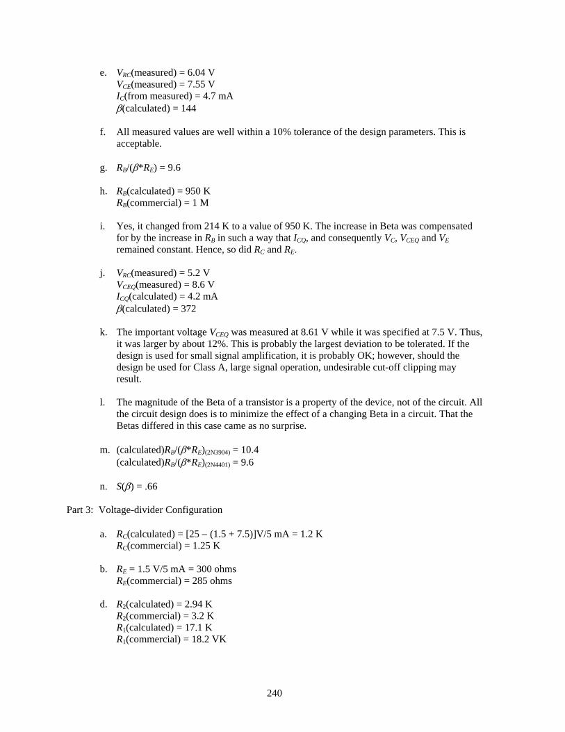
e. VRC(measured) = 6.04 V VCE(measured) = 7.55 V IC(from measured) = 4.7 mA β(calculated) = 144 f. All measured values are well within a 10% tolerance of the design parameters. This is
acceptable. g. RB/(β*RB E) = 9.6 h. RB(calculated) = 950 K B
RB(commercial) = 1 M B
i. Yes, it changed from 214 K to a value of 950 K. The increase in Beta was compensated
for by the increase in RB in such a way that IB CQ, and consequently VC, VCEQ and VE remained constant. Hence, so did RC and RE.
j. VRC(measured) = 5.2 V VCEQ(measured) = 8.6 V ICQ(calculated) = 4.2 mA β(calculated) = 372 k. The important voltage VCEQ was measured at 8.61 V while it was specified at 7.5 V. Thus,
it was larger by about 12%. This is probably the largest deviation to be tolerated. If the design is used for small signal amplification, it is probably OK; however, should the design be used for Class A, large signal operation, undesirable cut-off clipping may result.
l. The magnitude of the Beta of a transistor is a property of the device, not of the circuit. All
the circuit design does is to minimize the effect of a changing Beta in a circuit. That the Betas differed in this case came as no surprise.
m. (calculated)RB/(β*RB E)(2N3904) = 10.4 (calculated)RB/(β*RB E)(2N4401) = 9.6 n. S(β) = .66 Part 3: Voltage-divider Configuration a. RC(calculated) = [25 − (1.5 + 7.5)]V/5 mA = 1.2 K RC(commercial) = 1.25 K b. RE = 1.5 V/5 mA = 300 ohms RE(commercial) = 285 ohms d. R2(calculated) = 2.94 K R2(commercial) = 3.2 K R1(calculated) = 17.1 K R1(commercial) = 18.2 VK
240
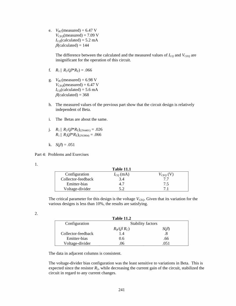
e. VRC(measured) = 6.47 V VCEQ(measured) = 7.09 V ICQ(calculated) = 5.2 mA β(calculated) = 144 The difference between the calculated and the measured values of ICQ and VCEQ are
insignificant for the operation of this circuit. f. R1 || R2/(β*RE) = .066 g. VRC(measured) = 6.98 V VCEQ(measured) = 6.47 V ICQ(calculated) = 5.6 mA β(calculated) = 368 h. The measured values of the previous part show that the circuit design is relatively
independent of Beta. i. The Betas are about the same. j. R1 || R2/(β*RE)(2N4401) = .026 R1 || R2(β*RE)(2N3904) = .066 k. S(β) = .051 Part 4: Problems and Exercises 1.
Table 11.1 Configuration ICQ (mA) VCEQ (V)
Collector-feedback 3.4 7.7 Emitter-bias 4.7 7.5
Voltage-divider 5.2 7.1
The critical parameter for this design is the voltage VCEQ. Given that its variation for the various designs is less than 10%, the results are satisfying.
2.
Table 11.2 Configuration Stability factors
RB/(β RB C) S(β) Collector-feedback 1.4 .8
Emitter-bias 0.6 .66 Voltage-divider .06 .051
The data in adjacent columns is consistent. The voltage-divider bias configuration was the least sensitive to variations in Beta. This is
expected since the resistor R2, while decreasing the current gain of the circuit, stabilized the circuit in regard to any current changes.
241
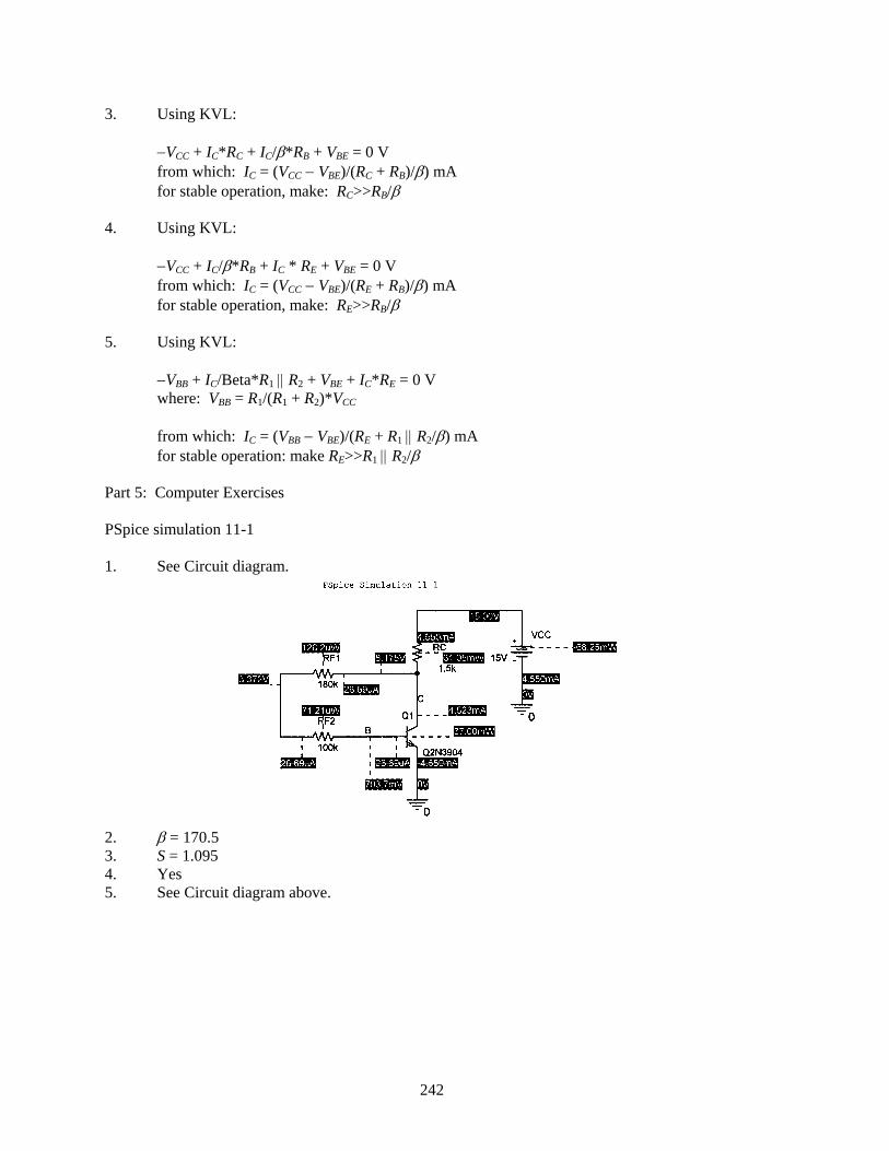
3. Using KVL: −VCC + IC*RC + IC/β*RB + VB BE = 0 V from which: IC = (VCC − VBE)/(RC + RB)/β) mA B
for stable operation, make: RC>>RB/β B
4. Using KVL: −VCC + IC/β*RB + IB C * RE + VBE = 0 V from which: IC = (VCC − VBE)/(RE + RB)/β) mA B
for stable operation, make: RE>>RB/β B
5. Using KVL: −VBB + IC/Beta*R1 || R2 + VBE + IC*RE = 0 V where: VBB = R1/(R1 + R2)*VCC from which: IC = (VBB − VBE)/(RE + R1 || R2/β) mA for stable operation: make RE>>R1 || R2/β Part 5: Computer Exercises PSpice simulation 11-1 1. See Circuit diagram.
2. β = 170.5 3. S = 1.095 4. Yes 5. See Circuit diagram above.
242
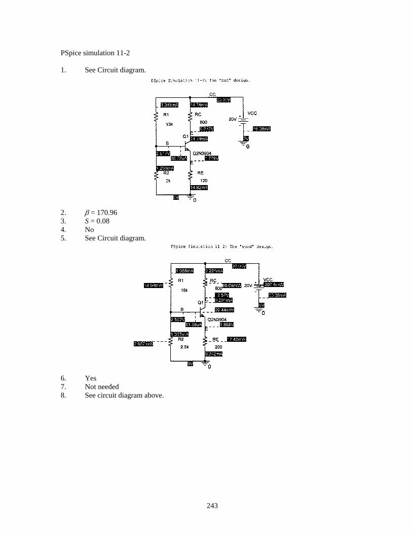
PSpice simulation 11-2 1. See Circuit diagram.
2. β = 170.96 3. S = 0.08 4. No 5. See Circuit diagram.
6. Yes 7. Not needed 8. See circuit diagram above.
243
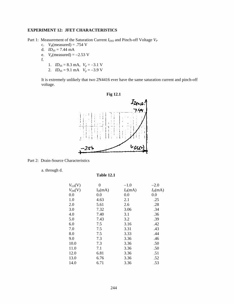
EXPERIMENT 12: JFET CHARACTERISTICS Part 1: Measurement of the Saturation Current IDSS and Pinch-off Voltage VP c. VR(measured) = .754 V d. IDSS = 7.44 mA e. Vp(measured) = −2.53 V f. 1. IDSS = 8.3 mA, Vp = −3.1 V 2. IDSS = 9.1 mA Vp = −3.9 V It is extremely unlikely that two 2N4416 ever have the same saturation current and pinch-off
voltage.
Fig 12.1
Part 2: Drain-Source Characteristics a. through d. Table 12.1
VGS(V) 0 −1.0 −2.0 VDS(V) ID(mA) ID(mA) ID(mA) 0.0 0.0 0.0 0.0 1.0 4.63 2.1 .25 2.0 5.61 2.6 .28 3.0 7.32 3.06 .34 4.0 7.40 3.1 .36 5.0 7.43 3.2 .39 6.0 7.5 3.16 .42 7.0 7.5 3.31 .43 8.0 7.5 3.33 .44 9.0 7.3 3.36 .46 10.0 7.3 3.36 .50 11.0 7.1 3.36 .50 12.0 6.81 3.36 .51 13.0 6.76 3.36 .52 14.0 6.71 3.36 .53
244
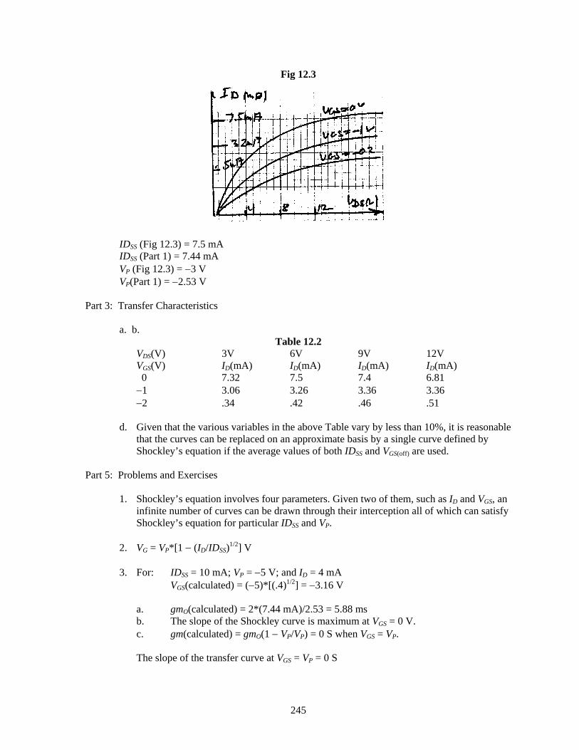
Fig 12.3
IDSS (Fig 12.3) = 7.5 mA IDSS (Part 1) = 7.44 mA VP (Fig 12.3) = −3 V VP(Part 1) = −2.53 V Part 3: Transfer Characteristics a. b.
Table 12.2 VDS(V) 3V 6V 9V 12V VGS(V) ID(mA) ID(mA) ID(mA) ID(mA) 0 7.32 7.5 7.4 6.81 −1 3.06 3.26 3.36 3.36 −2 .34 .42 .46 .51
d. Given that the various variables in the above Table vary by less than 10%, it is reasonable
that the curves can be replaced on an approximate basis by a single curve defined by Shockley’s equation if the average values of both IDSS and VGS(off) are used.
Part 5: Problems and Exercises 1. Shockley’s equation involves four parameters. Given two of them, such as ID and VGS, an
infinite number of curves can be drawn through their interception all of which can satisfy Shockley’s equation for particular IDSS and VP.
2. VG = VP*[1 − (ID/IDSS)1/2] V 3. For: IDSS = 10 mA; VP = −5 V; and ID = 4 mA VGS(calculated) = (−5)*[(.4)1/2] = −3.16 V a. gmO(calculated) = 2*(7.44 mA)/2.53 = 5.88 ms b. The slope of the Shockley curve is maximum at VGS = 0 V. c. gm(calculated) = gmO(1 − VP/VP) = 0 S when VGS = VP. The slope of the transfer curve at VGS = VP = 0 S
245
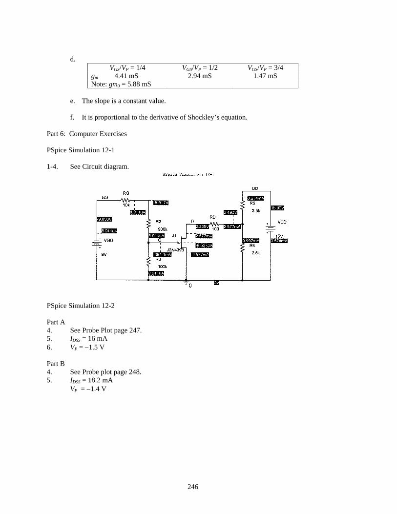
d.
VGS/VP = 1/4 VGS/VP = 1/2 VGS/VP = 3/4 gm 4.41 mS 2.94 mS 1.47 mS Note: gm0 = 5.88 mS
e. The slope is a constant value. f. It is proportional to the derivative of Shockley’s equation. Part 6: Computer Exercises PSpice Simulation 12-1 1-4. See Circuit diagram.
PSpice Simulation 12-2 Part A 4. See Probe Plot page 247. 5. IDSS = 16 mA 6. VP = −1.5 V Part B 4. See Probe plot page 248. 5. IDSS = 18.2 mA VP = −1.4 V
246
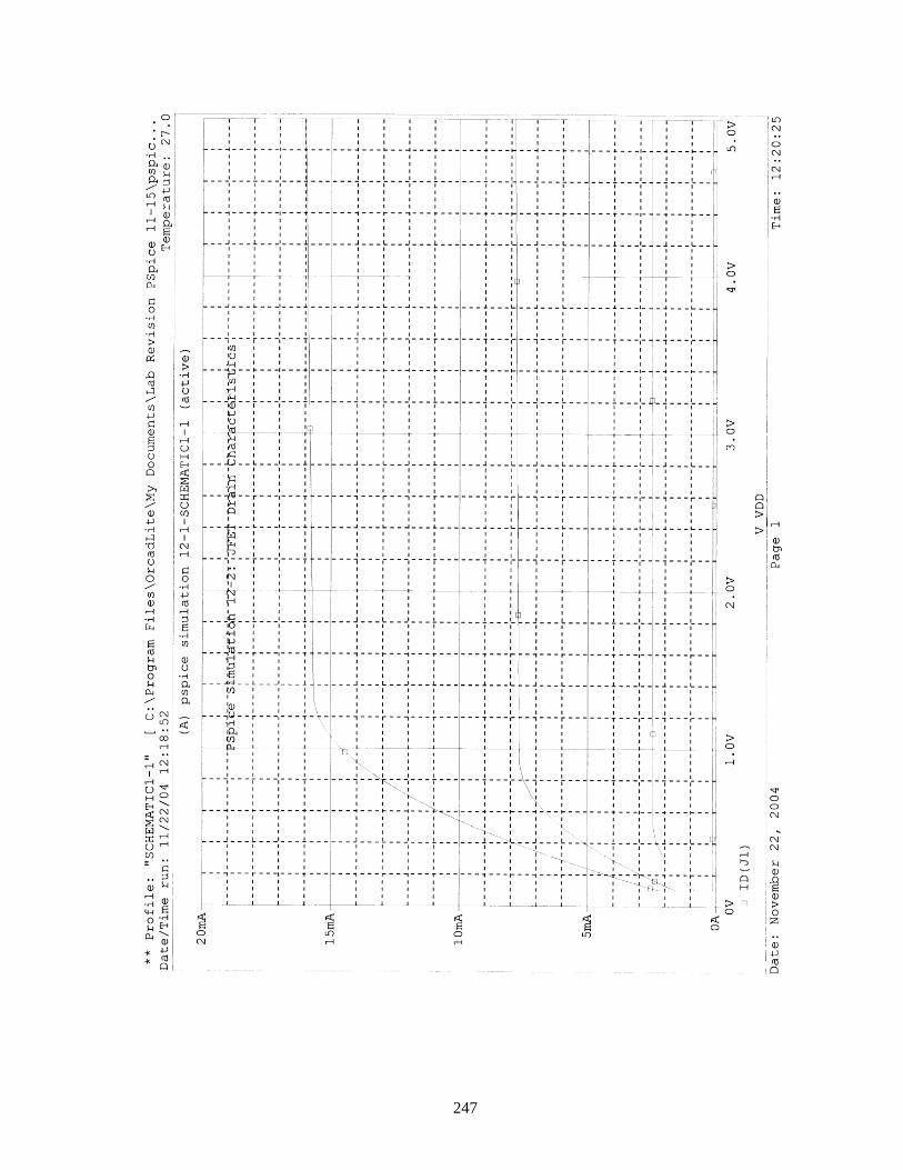
247
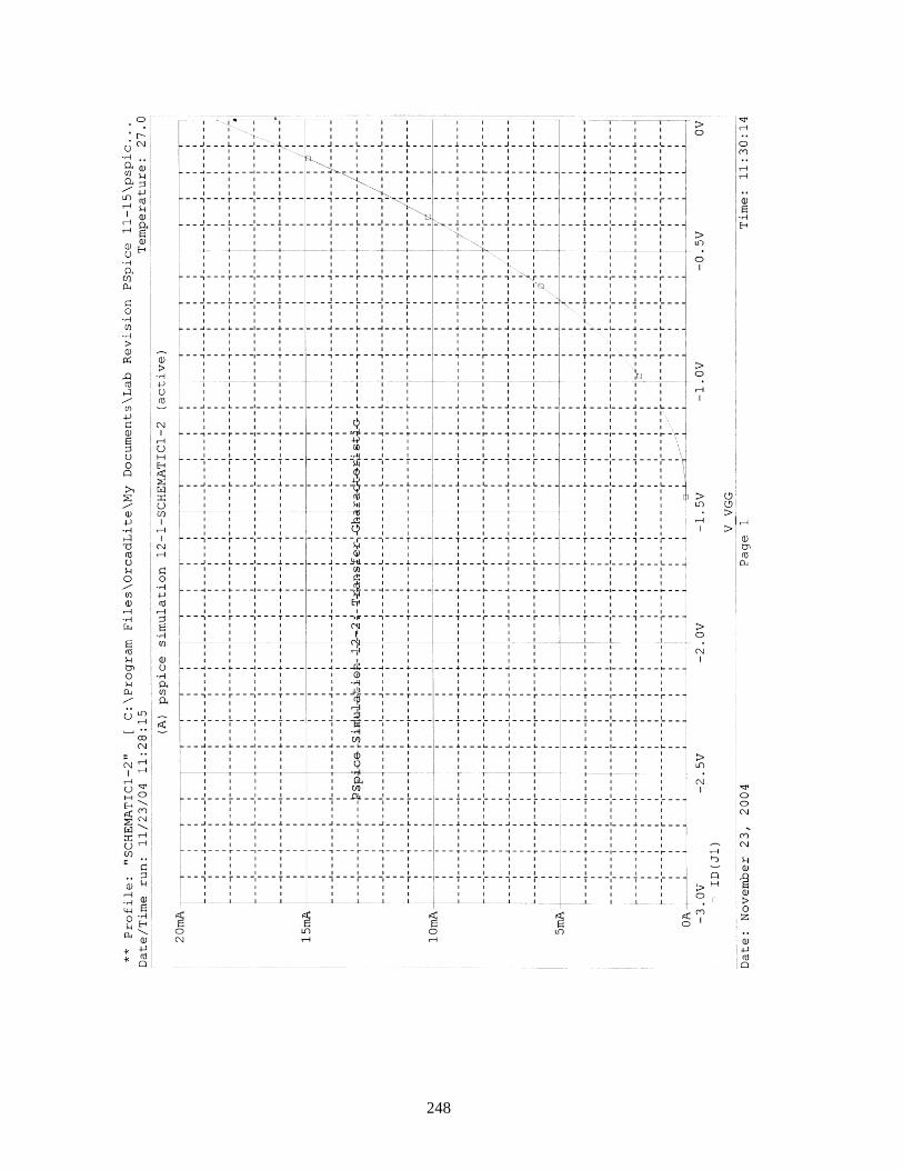
248
EXPERIMENT 13: JFET BIAS CIRCUITS Part 1: Fixed-Bias Network b. IDSS = 12 mA c. VP(measured) = −6 V e. ID = 12−3(1 − 1/6)1/2 = 8.33 mA f. VRD(measured) = 8 V IDQ(measured) = 8.2 mA RD(measured) = 976 ohms Part 2: Self-Bias Network b. IDQ = 2.64 mA VGSQ = −3.3 V c. VGS(calculated) = −3.3 V VD(calculated) = 12.4 V VS(calculated) = 3.1 V VDS(calculated) = 9.3 V VG(calculated) = 0 V d. VGS(measured) = −3.4 V VD(measured) = 12.2 V VS(measured) = 2.1 V VDS(measured) = 9.1 V VG(measured) = 0 V The percent differences are determined with the calculated values as the reference. VGS(calculated %) = 3.1% VD(calculated %) = −1.6% VS(calculated %) = −.64% VDS(calculated %) = −2.3% VG(calculated %) = 0% Part 3: Voltage Divider-Bias Network b. For voltage divider-bias-line see Fig. 13.2 c. IDQ(calculated) = 4.8 mA VGS(calculated) = −2.4 V d. VD(calculated) = 10.3 V VS(calculated) = 5.2 V VDS(calculated) = 5.1 V e. VGSQ(measured) = −2.3 V VD(measured) = 10.4 V VS(measured) = 5.3 V VDS(measured) = 5.1 V
249
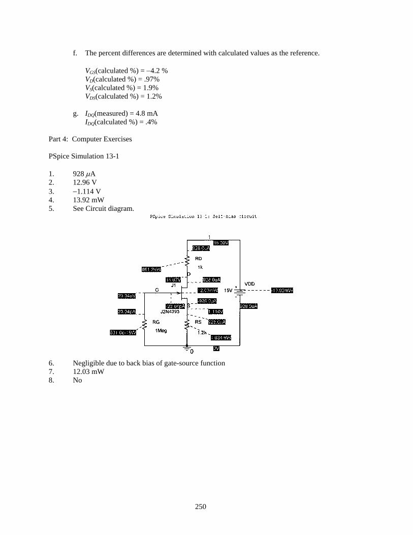
f. The percent differences are determined with calculated values as the reference. VGS(calculated %) = −4.2 % VD(calculated %) = .97% VS(calculated %) = 1.9% VDS(calculated %) = 1.2% g. IDQ(measured) = 4.8 mA IDQ(calculated %) = .4% Part 4: Computer Exercises PSpice Simulation 13-1 1. 928 μA 2. 12.96 V 3. −1.114 V 4. 13.92 mW 5. See Circuit diagram.
6. Negligible due to back bias of gate-source function 7. 12.03 mW 8. No
250
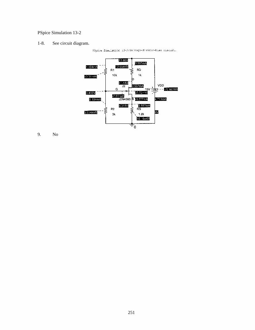
PSpice Simulation 13-2 1-8. See circuit diagram.
9. No
251
EXPERIMENT 14: DESIGN OF JFET BIAS CIRCUITS Part 1: Determining IDSS and VP b. IDSS(measured) = 10.8 mA c. VP(measured) = −6 V Part 2: Self-bias Circuit Design a. IDQ(calculated) = 5.4 mA VDSQ(calculated) = 15 V VDD(calculated) = 30 V d. RS(calculated) = 1/gm = 333 ohms RS(commercial) = 330 ohms e. VRD = VDD − VDSQ − VRS = 30 − 15 − 1.8 = 13.2 V RD = 2.4 K f. VDSQ(measured) = 14.7 V IDQ(measured) = 5.6 mA VDSQ(calculated) = 15 V IDQ(calculated) = 5.4 mA g. Agreements between calculated and measured values are within 10% of each other and
thus are within acceptable limits. h. VDSQ(measured) = 13.7 V IDQ(measured) = 6 mA IDSS(borrowed JFET) = 9.8 mA VP(borrowed JFET) = −5.1 V Even though in our case, the variations between JFETs was relatively small, such may
not be the case in general. Thus, the values of the biasing resistors for the same bias design but employing different JFETs may differ considerably.
Best is not to use the arithmetic but the geometric average for the range of IDSS and VP.
Thus in our case, the geometric averages would be: IDSS(geometric average) = [IDSS(min) * IDSS(max)]1/2 = [5 mA*15mA)]1/2
= 8.66 mA VP (geometric average) = [1*6]1/2 = 2.45 V Statistically, these values are most likely the ones encountered. Part 3: Voltage-divider Circuit Design a. VGS(calculated) = −2.6 V b. RS = (VGG − VGS)/IDQ = (6 − 2.6)V/4 mA = 850 ohms RS(commercial value) = 820 ohms VG(calculated) = VGS + ID*RS = 2.6 + 4 mA*820 = 5.85 V
252
c. VRD(calculated) = VDD − VDSQ − VRS = 20 − 8 − 3.28 = 8.72 V where VRS = IDQ*RS = 4 mA*820 = 3.28 V RD = [VDD −(VDSQ + VRS)]/ID = [20 − (8 + 3.28)] = 2.18 Kohms RD(commercial value) = 2 Kohms d. R2 = 10*RS = 10*820 = 8.2 Kohms R2(commercial value) = 10 Kohms Solving equation 14.3 for R1 we obtain: R1 = R2*(VDD − VG)/VG = 10 K*(20 − 5.85)/5.85 = 24.2 Kohms R1(commercial value) = 22 Kohms e. VDSQ(measured) = 7.9 V IDQ(measured) = 4.2 mA VDSQ(specified) = 8 V IDQ(specified) = 4 mA f. %IDQ(calculated) = 5% %VDSQ(calculated) = −1.25% Such relative small percent deviations are almost too good to be true. The voltage divider bias line is parallel to the self-bias line. To shift the Q point in either
direction, it is easiest to adjust the bias voltage VG to bring the circuit parameters within an acceptable range of the circuit design.
g. In the present case, the percent differences for IDQ and VDSQ were well within the 10%
tolerance allowed. If not, the easiest adjustment would be the moving of the voltage-divider bias line parallel to itself by means of raising or lowering of VG. This could best be accomplished by a change of the voltage divider R2/(R1 + R2)*VDD. Its value determines the voltage VG which in turn determines the Q point for the design.
h. VDSQ(measured) = 13.7 V IDQ(measured) = 3.68 mA IDSS(borrowed JFET) = 9.8 mA VP(borrowed JFET) = −5.1 V Part 4: Problems and Exercises 1. RD(commercial value) = 2.7 Kohms RS(commercial value) = 180 ohms 2. RD(commercial value) = 2.4 Kohms RS(commercial value) = 680 ohms R1(commercial value) = 6.8 Kohms R2(commercial value) = 33 Kohms
253
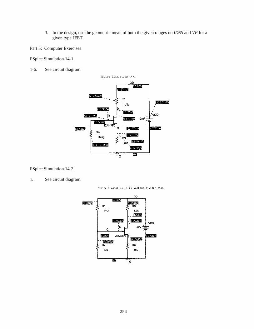
3. In the design, use the geometric mean of both the given ranges on IDSS and VP for a given type JFET.
Part 5: Computer Exercises PSpice Simulation 14-1 1-6. See circuit diagram.
PSpice Simulation 14-2 1. See circuit diagram.
254
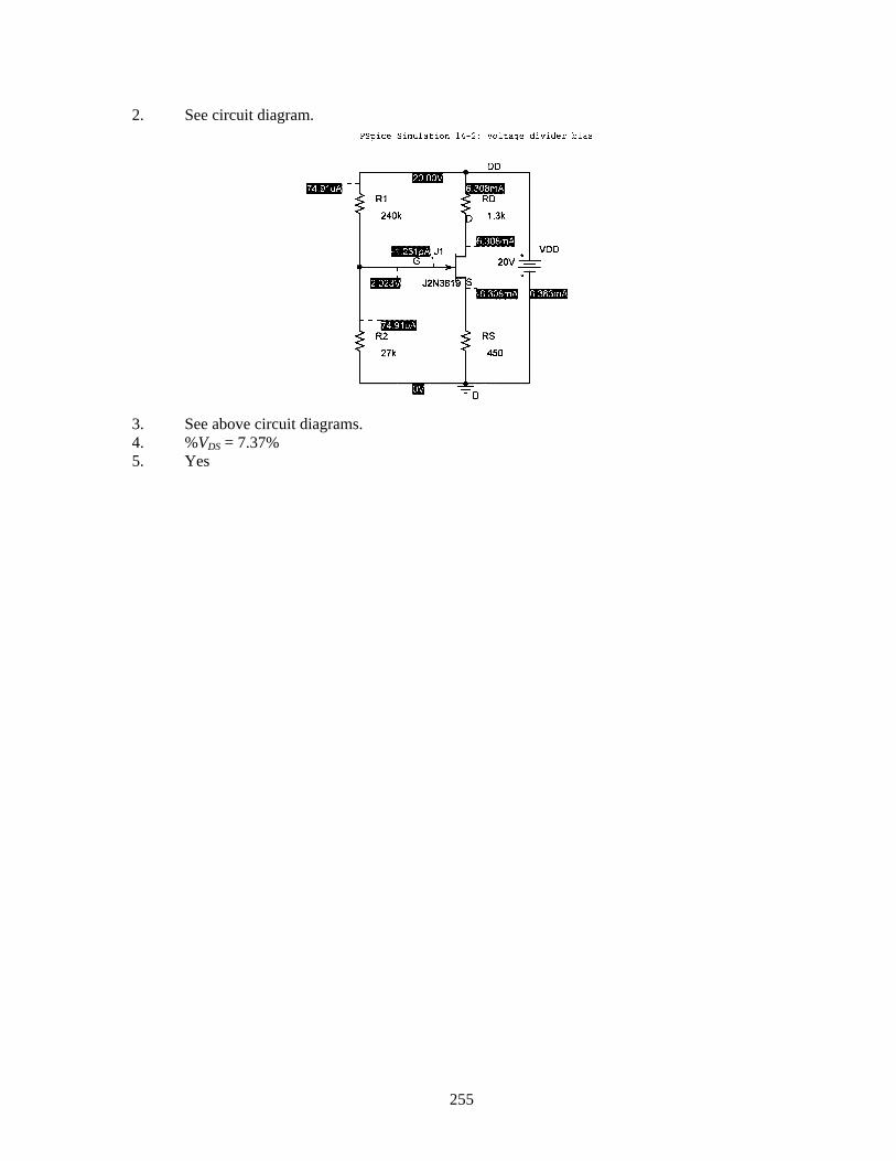
2. See circuit diagram.
3. See above circuit diagrams. 4. %VDS = 7.37% 5. Yes
255
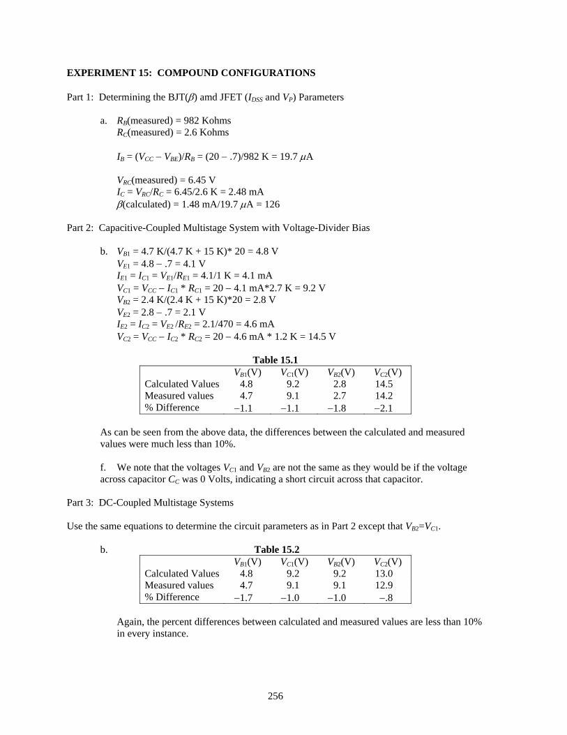
EXPERIMENT 15: COMPOUND CONFIGURATIONS Part 1: Determining the BJT(β) amd JFET (IDSS and VP) Parameters a. RB(measured) = 982 Kohms B
RC(measured) = 2.6 Kohms IB = (VB CC − VBE)/RBB = (20 − .7)/982 K = 19.7 μA VRC(measured) = 6.45 V IC = VRC/RC = 6.45/2.6 K = 2.48 mA β(calculated) = 1.48 mA/19.7 μA = 126 Part 2: Capacitive-Coupled Multistage System with Voltage-Divider Bias b. VB1 = 4.7 K/(4.7 K + 15 K)* 20 = 4.8 V VE1 = 4.8 − .7 = 4.1 V IE1 = IC1 = VE1/RE1 = 4.1/1 K = 4.1 mA VC1 = VCC − IC1 * RC1 = 20 − 4.1 mA*2.7 K = 9.2 V VB2 = 2.4 K/(2.4 K + 15 K)*20 = 2.8 V VE2 = 2.8 − .7 = 2.1 V IE2 = IC2 = VE2 /RE2 = 2.1/470 = 4.6 mA VC2 = VCC − IC2 * RC2 = 20 − 4.6 mA * 1.2 K = 14.5 V
Table 15.1 VB1(V) VC1(V) VB2(V) VC2(V) Calculated Values 4.8 9.2 2.8 14.5 Measured values 4.7 9.1 2.7 14.2 % Difference −1.1 −1.1 −1.8 −2.1
As can be seen from the above data, the differences between the calculated and measured
values were much less than 10%. f. We note that the voltages VC1 and VB2 are not the same as they would be if the voltage
across capacitor CC was 0 Volts, indicating a short circuit across that capacitor. Part 3: DC-Coupled Multistage Systems Use the same equations to determine the circuit parameters as in Part 2 except that VB2=VC1. b. Table 15.2
VB1(V) VC1(V) VB2(V) VC2(V) Calculated Values 4.8 9.2 9.2 13.0 Measured values 4.7 9.1 9.1 12.9 % Difference −1.7 −1.0 −1.0 −.8
Again, the percent differences between calculated and measured values are less than 10%
in every instance.
256
f. The dc collector voltage of stage 1 determines the dc base voltage of stage 2. Note that no biasing resistors are needed for stage 2.
Part 4: A BJT-JFET Compound Configuration b. VB = 4.7 K/(4.7 k + 15 k) * 30 = 7.2 V B
VE = VB − .7 V = 6.5 V B
IE = ID = 6.5 V/1.2 K = 5.4 mA VD = VDD*RD = 30 − 5.4 mA*985 = 24.7 V For the JFET used: IDSS = 10.1 mA VP = −3.2 V determine VGS: ID/IDSS = [1 − VGS/VP]1/2
mA = 5.4 mA/10.1 mA = [1 − VGS/3.2]1/2 mA therefore: [5.4 mA/10.1 mA]2 = [1 − VGS/3.2] .286 = [1 − VGS/3.2] from which: VGS = (1 − .286)*3.2 = −2.28 V remember: VGS is a negative number: VC = VB − VB GS = 7.2 − (−2.28) = 9.5 V
Table 15.3 VB(V) B VD(V) VC(V) Calculated Values 7.2 23.6 9.5 Measured values 7.1 24.4 8.7 % Difference −.56 3.4 −8.4
d. See Table 15.3. e. Differences were less than 10%. f. VGS(calculated from measured values) = VB − VB C = 7.1 − 8.7 = −1.6 V VGS(measured) = −1.7 V g. VRD = VDD − VD = 30 − 24.7 = 5.3 V ID = 5.3 V/985 = 5.4 mA ID(measured) = 6.4 mA The percent difference between the measured and the calculated values of ID was 18.5%,
with the calculated value of ID used as the standard of reference. VE(calculated) = 7.2 − .7 = 6.5 V IC(calculated) = 6.5 V/1.26 K = 5.2 mA IC(measured) = 5.06 mA
257
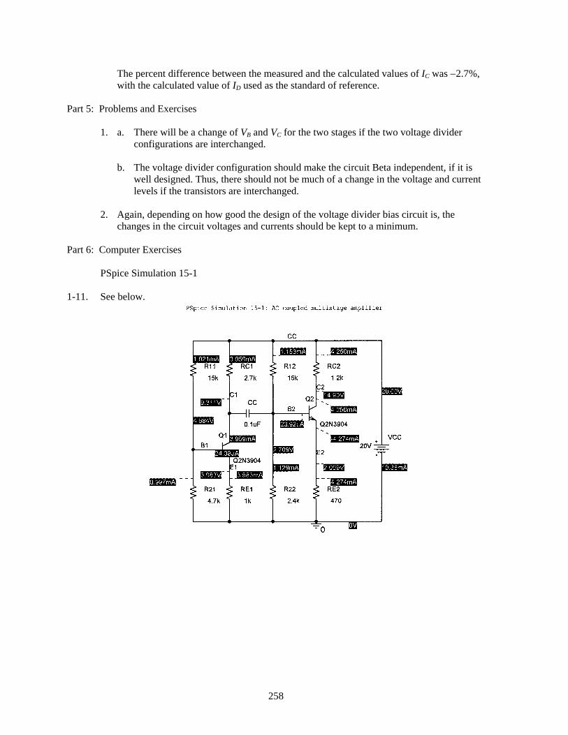
The percent difference between the measured and the calculated values of IC was −2.7%, with the calculated value of ID used as the standard of reference.
Part 5: Problems and Exercises 1. a. There will be a change of VB and VB C for the two stages if the two voltage divider
configurations are interchanged. b. The voltage divider configuration should make the circuit Beta independent, if it is
well designed. Thus, there should not be much of a change in the voltage and current levels if the transistors are interchanged.
2. Again, depending on how good the design of the voltage divider bias circuit is, the
changes in the circuit voltages and currents should be kept to a minimum. Part 6: Computer Exercises PSpice Simulation 15-1 1-11. See below.
258
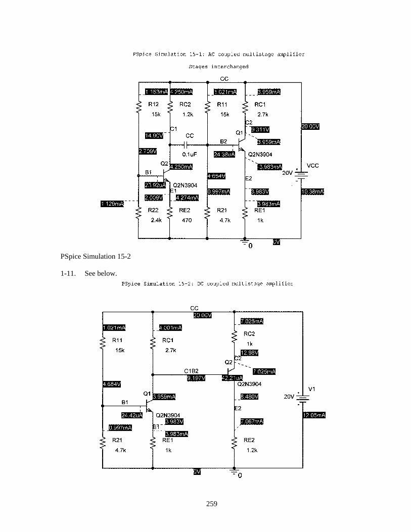
PSpice Simulation 15-2 1-11. See below.
259
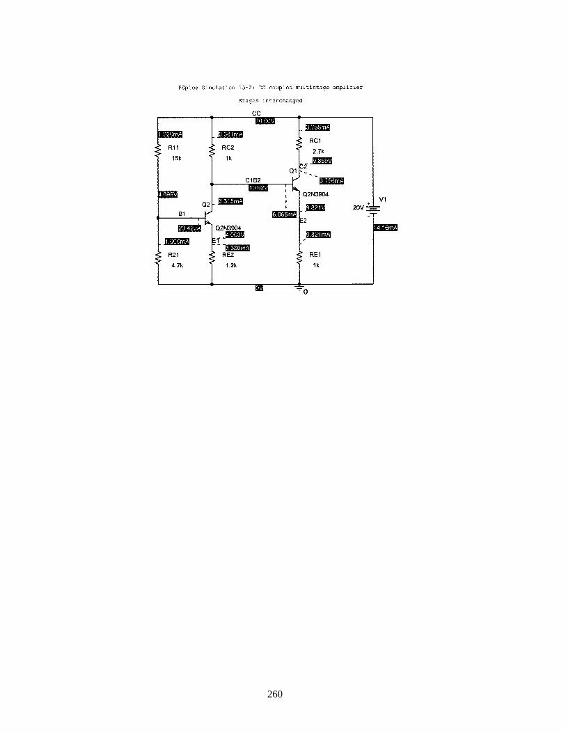
260
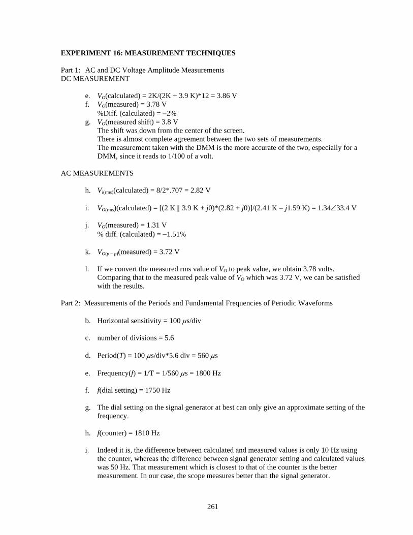
EXPERIMENT 16: MEASUREMENT TECHNIQUES Part 1: AC and DC Voltage Amplitude Measurements DC MEASUREMENT e. VO(calculated) = 2K/(2K + 3.9 K)*12 = 3.86 V f. VO(measured) = 3.78 V %Diff. (calculated) = −2% g. VO(measured shift) = 3.8 V The shift was down from the center of the screen. There is almost complete agreement between the two sets of measurements. The measurement taken with the DMM is the more accurate of the two, especially for a
DMM, since it reads to 1/100 of a volt. AC MEASUREMENTS h. Vi(rms)(calculated) = 8/2*.707 = 2.82 V i. VO(rms)(calculated) = [(2 K || 3.9 K + j0)*(2.82 + j0)]/(2.41 K − j1.59 K) = 1.34∠33.4 V j. VO(measured) = 1.31 V % diff. (calculated) = −1.51% k. VO(p − p)(measured) = 3.72 V l. If we convert the measured rms value of VO to peak value, we obtain 3.78 volts.
Comparing that to the measured peak value of VO which was 3.72 V, we can be satisfied with the results.
Part 2: Measurements of the Periods and Fundamental Frequencies of Periodic Waveforms b. Horizontal sensitivity = 100 μs/div c. number of divisions = 5.6 d. Period(T) = 100 μs/div*5.6 div = 560 μs e. Frequency(f) = 1/T = 1/560 μs = 1800 Hz f. f(dial setting) = 1750 Hz g. The dial setting on the signal generator at best can only give an approximate setting of the
frequency. h. f(counter) = 1810 Hz i. Indeed it is, the difference between calculated and measured values is only 10 Hz using
the counter, whereas the difference between signal generator setting and calculated values was 50 Hz. That measurement which is closest to that of the counter is the better measurement. In our case, the scope measures better than the signal generator.
261
Part 3: Phase-Shift Measurements b. Vi(rms)(calculated) = 6/2*.707 = 2.12 V c. VO(rms) = (0 − j1.59 K)*(2.12 + j0)/(1k − j1.59 K) = 1.81∠−31.6 V VO(p−p)(rms) = 1.81*1.41*2 = 5.1 V f. A(number of divisions) = .8 g. B(number of divisions) = 10 h. angle θ(calculated) = −31.6 degrees j. The network is a lag network, i.e., the output voltage VO lags the input voltage by the
angle theta, in our case it lags it by −31.6 degrees. k. VR(rms)(calculated) = 1.1 V VR(p−p)(calculated) = 3.1 V angle theta = 58.4 degrees The output voltage VO leads the input voltage by 58.4 degrees. Note that an angle of 58.4
degrees is the complement of an angle of 31.6 degrees. l. VR(p−p)(measured) = 3 V angle θ = 58 degrees It’s a lead angle. Part 4: Loading Effects c. VO(p−p)(calculated) = 1 K/(1 K + 1 K)*8 = 4 V d. VO(p−p)(measured) = 3.98 V f. VO(p−p)(calculated) = 1 M/(1 M + 1 M)*8 = 4 V VO(p−p)(measured) = 2.7 V g. The real part of the input impedance of the scope is now in parallel with the R2 resistor
and since for many scopes, that real part is about 1 Mohm, therefore, Rscope || R2 = 500 kohms.
Thus, VO is considerably reduced. h. R(prime) = 1 M/[Vi/VO − 1] = 1 M/[8/2.7 − 1] = 588 kohms R(scope) = −R(prime)*R2/[R(prime) − R2] = 1.43 Megohms Most general purpose oscilloscopes have an input impedance consisting of a real part of 1 Megohms in parallel with a 30 pf capacitor. The result obtained for the real part of that
impedance is reasonably close to that. i. VO(p−p)(calculated) = 1 K/(1 K + 1 M)*8 = 8 mV j. VO(p−p)(measured) = 7.9 mV k. The results agree within 1.25 percent.
262
Part 5: Problems and Exercises 1. No. for the frequency of operation, the capacitor represents an impedance of 1.59k∠−90
ohms. Therefore, in relationship to the existing resistors in the circuit, it cannot be neglected without making a serious error.
2. It depends upon the waveform. In case of sinusoidal voltages, the advantage is probably
with the DMM. For more complex waveforms, the nod goes to the oscilloscope. 3. For measuring sinusoidal waves, the DMM gives a direct reading of the rms value of the
measured waveform. However, for non-sinusoidal waves, a true rms DMM must be employed. The oscilloscope only gives peak-peak values, which, if one wants to obtain the power in an ac circuit, must be converted to rms.
4. T = 5 div*.1 ms/div = .5 ms f = 1/T = 1/.5 ms = 2 KHz 5. angle theta = 1.5/8*360 = 67.5 degrees VO/Vi = R′/(R′ + R1) therefore: Vi/VO = (R′ + R1)/R′ solving for R′: R′(Vi/VO) = R′ + R1
R′(Vi/VO − 1) = R1
Hence: R′ = R1/(Vi/VO − 1) ohms Part 6: Computer Exercises PSpice Simulation 16-1 1. See Probe plot page 264. 2. See Probe plot page 264. 3. See Probe plot page 265. 4. See Probe plot page 265. 5. 33.74° 6. Vout 9. See Probe plot page 266. 10 See Probe plot page 266. 11. Vin(rms) = 2.84 V Vout(rms) = 1.32 V 12. Yes 13. See Probe plot page 267. 14. See Probe plot page 267.
15. Vout = 3 2 K(12 V) = (12 V)2 3 (212 + 3.9 K)R
R R+
= 4.067 V 16. Agree
263
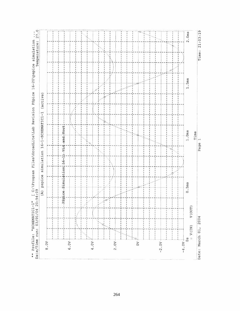
264
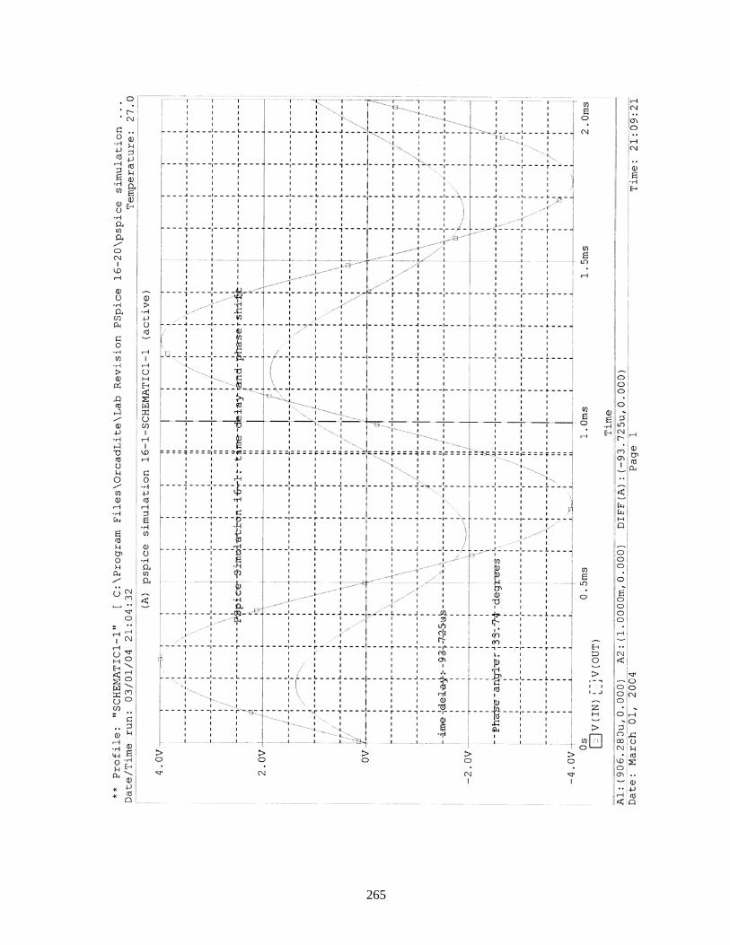
265
266
267
PSpice Simulation 16-2 1. Using VOM, R2 = 100 kΩ 2. Using DMM, R2 = 1 kΩ 3. For R2 = 1 kΩ 4. Both circuits 5. No
268
EXPERIMENT 17: COMMON-EMITTER TRANSISTOR AMPLIFIERS Part 1: Common-Emitter DC Bias b. VBB = R2/(R1 + R2) * VCC = 10 K/(10 K + 33 K) * 10 = 2.33 V VE = VBB − .7 = 1.63 V VC = VCC − IC * RC = 10 − 1.63 mA * 3 K = 5.1 V IE = VE/RE = 1.63/1 K = 1.63 mA re = 26 mV/IE = 26 mV/1.63 mA = 16 ohms c. VB(measured) = 2.25 V B
VE(measured) = 1.57 V VC (measured) = 4.95 V IE = VE/RE = 1.57/978 = 1.6 mA re = 26 mV/1.6 mA = 16.2 ohms The two values for re obtained are within .2 ohms. This represents a 1.25 percent difference. Part 2: Common-Emitter AC Voltage Gain a. AV(no load) = −RC/re = 3.2 K/16 = 198 b. Vsig = 8.3 mV(rms) VO(no load) = 1.47 V (rms) AV(no load) = 177 The two values of AV agree within 10.6 percent of each other. Part 3: AC Input Impedance, Zi Zin = R1 || R2 || Beta * re = 10 K || 33 K || (150 * 16) = 1.8 Kohms Vi (measured) = 12 mV (rms) Vsig = 20 mV(rms) Zin = [12 mV/(20 mV − 12 mV)] * 1 K = 1.5 Kohms The two values of the input impedance were within 18.9% of each other. This relatively large divergence is in part the result of using an assumed value of Beta for our transistor. For a 2N3904 transistor, the geometric average of Beta is closer to 126. Part 4: Output Impedance a. ZO(calculated) = RC = 3.2 Kohms b. Vsig(rms) = 10 mV(rms) VO(no load)(rms) = 1.8 V (rms) VO(loaded)(rms) = .913 V(rms) RL = 3.2 Kohms ZO = [(VO − VL)/VL] * RL = [(1.8 − .913)/.913] * 3.2 K = 3.1 K The two values for ZO are within 3.15% of each other.
269
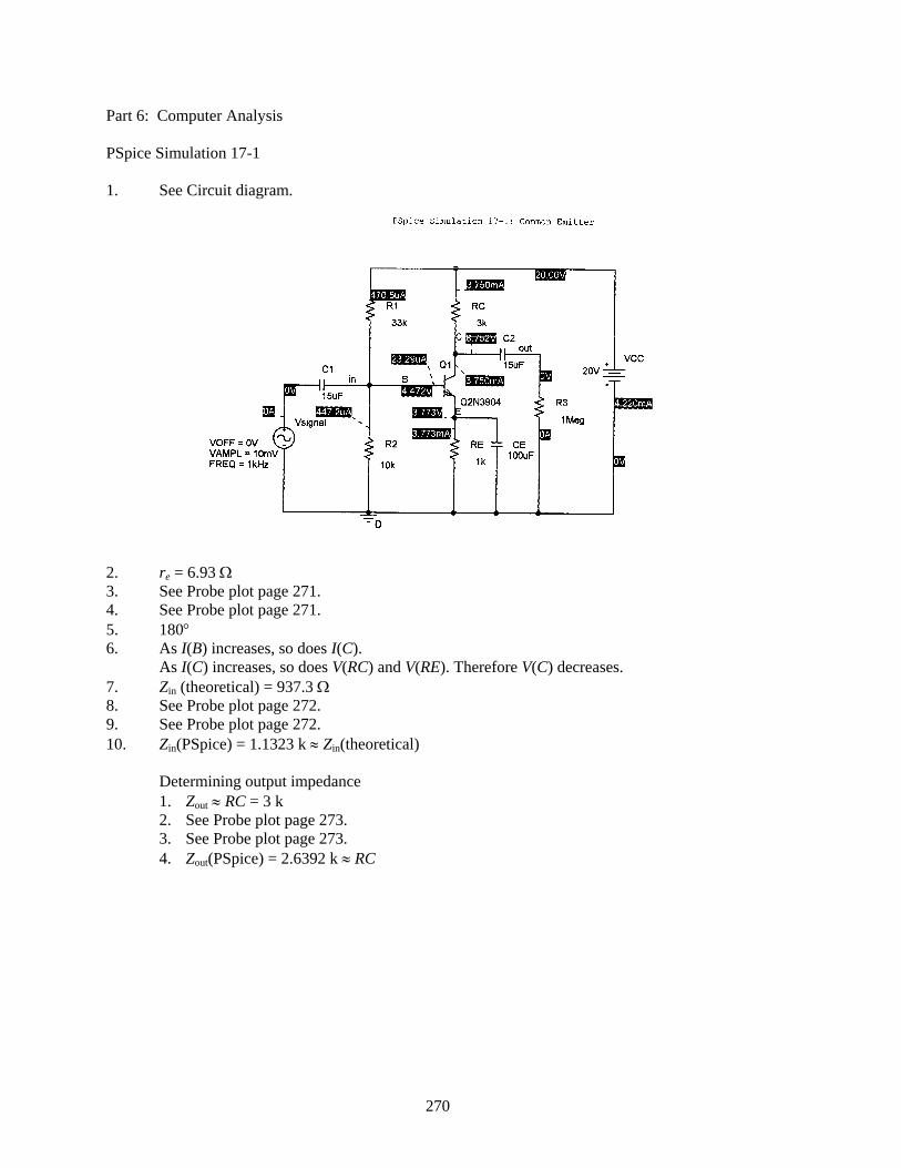
Part 6: Computer Analysis PSpice Simulation 17-1 1. See Circuit diagram.
2. re = 6.93 Ω 3. See Probe plot page 271. 4. See Probe plot page 271. 5. 180° 6. As I(B) increases, so does I(C). As I(C) increases, so does V(RC) and V(RE). Therefore V(C) decreases. 7. Zin (theoretical) = 937.3 Ω 8. See Probe plot page 272. 9. See Probe plot page 272. 10. Zin(PSpice) = 1.1323 k ≈ Zin(theoretical) Determining output impedance 1. Zout ≈ RC = 3 k 2. See Probe plot page 273. 3. See Probe plot page 273. 4. Zout(PSpice) = 2.6392 k ≈ RC
270
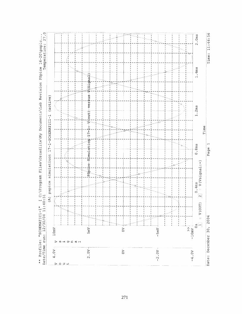
271
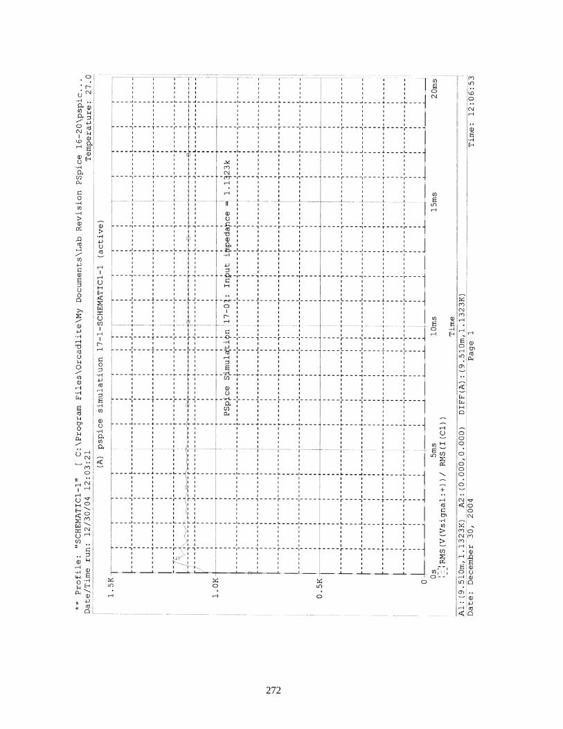
272
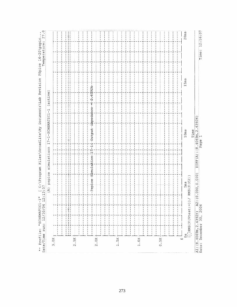
273
EXPERIMENT 18: COMMON-BASE AND EMITTER-FOLLOWER (COMMON-COLLECTOR TRANSISTOR AMPLIFIERS Part 1: Common-Base DC Bias a. VB(calculated) = 10 K/(10 K + 33 K) * 10 = 2.33 V B
VE = VB − .7 V = 1.63 V B
IE = IC = VE/RE = 1.63 V/1 K = 1.63 mA VC = 10 − IC * RC = 10 − (1.63 mA) * 3 K = 5.1 V re = 26 mV/IE = 26 mV/1.63 mA = 16 ohms b. VB(measured) = 2.26 V B
VE(measured) = 1.57 V VC(measured) = 4.95 V IE(from measured values) = VE/RE = 1.57 V/978 = 1.6 mA re(from measured values) = 26 mV/IE = 26 mV/1.6 = 16.3 ohms In every case, the differences between the two sets of values are less than 10% apart.
Such divergence is not excessive given the variability of electronic components. Part 2: Common-Base AC Voltage Gain a. AV(calculated) = RC/re = 3.2 K/16.3 = 197 b. Vsig = 50 mV VO = 2.43 V AV = 2.43/Vsig = 2.43/.05 = 122 The two gains differed by −38 percent with the calculated gain used as the standard of
comparison. Part 3: CB Input Impedance, Zi a. Zi = re = 16.3 ohms b. Vsig = 50 mV Vi = 9.9 mV RX = 100 ohms Zi = [Vi/(Vsig − Vi)] * RX = [9.9 mV/(50 mV − 9.9 mV)] * 100 = 23.7 ohms The two values of the input impedance differed by 45 percent with the theoretical value
of re (16.3 ohms) used as the standard of comparison. Part 4: CB Output Impedance, ZO a. ZO = RC = 3.2 K b. Vsig = 20 mV VO(measured, no load) = 2.43 V VL(measured, loaded) = 1.22 V ZO = [(VO − VL)/VL] * RL = [(2.43 − 1.22)/1.22] * 3 K = 3.18 Kohms The agreement between the two values of the output impedance is within less than 1
percent.
274
Part 5: Emitter-Follower DC Bias a. VB(calculated) = 2.33 V B
VE(calculated) = 1.63 V IE(calculated) = 1.63 V VC(calculated) = 10 V re(calculated) = 26 mV/IE = 26 mV/1.63 mA = 16 ohms b. VB(measured) = 2.26 V B
VE(measured) = 1.78 V VC(measured) = 10.1 V IE = VE/RE = 1.78 V/1 K = 1.78 mA re = 26 mV/1.78 mA = 14.3 ohms Part 6: Emitter-Follower AC Voltage Gain a. AV = RE/(RE + re) = 1 K/(1 K + 14.3) = .986 b. Vsig = 1 V VO(measured) = .987 V AV = VO/Vsig = .987/1 = .987 The two values of gain are within .1 percent of each other. Part 7: Emitter Follower (EF) Input Impedance, Zi a. Zi = R1 || R2 || (Beta * (1 K + re) = 7.31 Kohms b. Vsig = 2 V RX = 10 Kohms f = 1 KHz Vi(measured) = .85 V Zi = [Vi/(Vsig − Vi)] * RX = [.85/(2 − .85)] * 10 K = 7.39 Kohms The input impedance calculated from measured values is within 1.1 percent of the
theoretically calculated value of Zi. Part 8: Emitter Follower (EF) Output Impedance, ZO a. ZO = re = 16 ohms b. VO(measured) = 19.8 mV VL(measured) = 11.2 mV ZO = [(VO − VL)/VL]*RL = [(19.8 mV − 11.2 mV)/11.2 mV] * 100 = 76.8 ohms In the theoretical formulation, ZO was equated with re, this is an approximation. A better
expression for the output impedance is: ZO = re + (RG || R1 || R2)/Beta. Thus it can be seen that the given formulation was actually a minimum value of the output impedance.
275
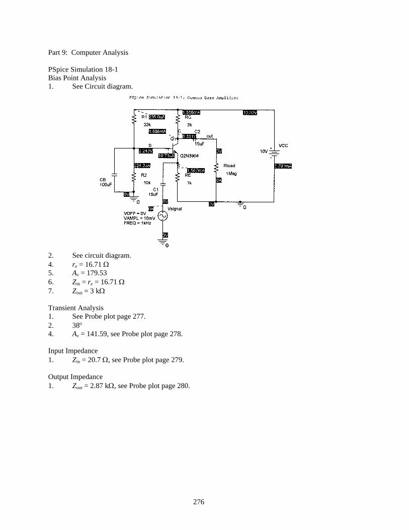
Part 9: Computer Analysis PSpice Simulation 18-1 Bias Point Analysis 1. See Circuit diagram.
2. See circuit diagram. 4. re = 16.71 Ω 5. Av = 179.53 6. Zin = re = 16.71 Ω 7. Zout = 3 kΩ Transient Analysis 1. See Probe plot page 277. 2. 38° 4. Av = 141.59, see Probe plot page 278. Input Impedance 1. Zin = 20.7 Ω, see Probe plot page 279. Output Impedance 1. Zout = 2.87 kΩ, see Probe plot page 280.
276
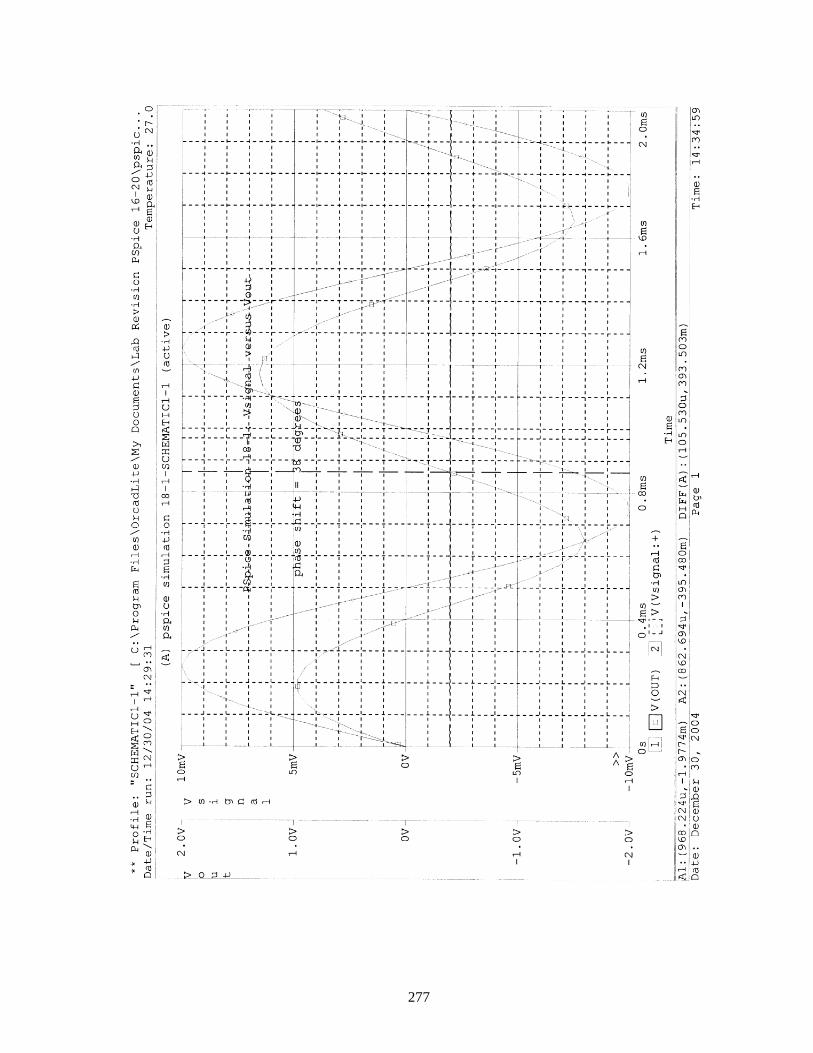
277
278
279
280
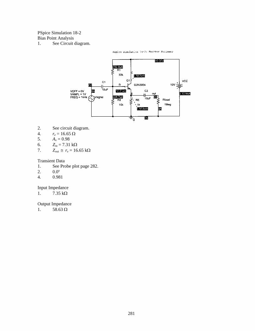
PSpice Simulation 18-2 Bias Point Analysis 1. See Circuit diagram.
2. See circuit diagram. 4. re = 16.65 Ω 5. Av = 0.98 6. Zin = 7.31 kΩ 7. Zout r≅ e = 16.65 kΩ Transient Data 1. See Probe plot page 282. 2. 0.0° 4. 0.981 Input Impedance 1. 7.35 kΩ Output Impedance 1. 58.63 Ω
281
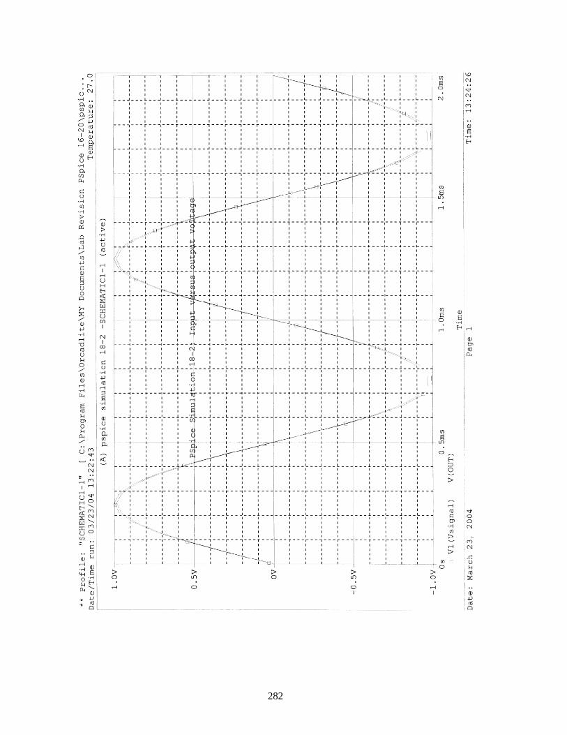
282
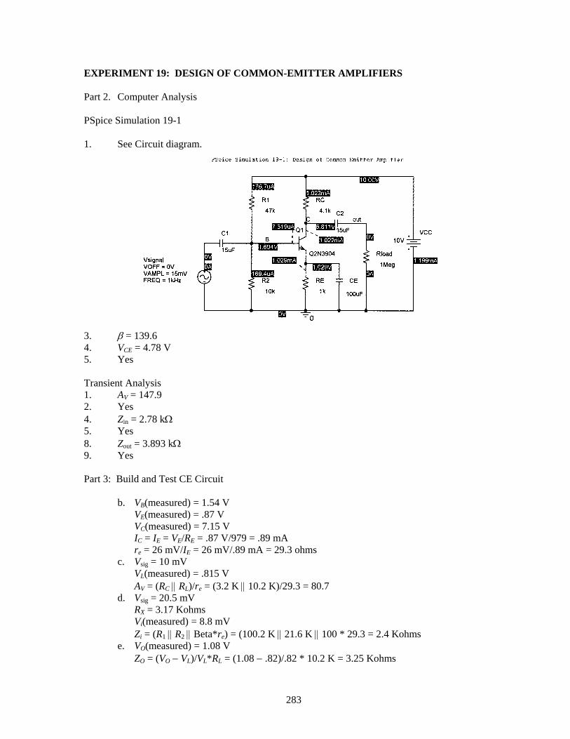
EXPERIMENT 19: DESIGN OF COMMON-EMITTER AMPLIFIERS Part 2. Computer Analysis PSpice Simulation 19-1 1. See Circuit diagram.
3. β = 139.6 4. VCE = 4.78 V 5. Yes Transient Analysis 1. AV = 147.9 2. Yes 4. Zin = 2.78 kΩ 5. Yes 8. Zout = 3.893 kΩ 9. Yes Part 3: Build and Test CE Circuit b. VB(measured) = 1.54 V B
VE(measured) = .87 V VC(measured) = 7.15 V IC = IE = VE/RE = .87 V/979 = .89 mA re = 26 mV/IE = 26 mV/.89 mA = 29.3 ohms c. Vsig = 10 mV VL(measured) = .815 V AV = (RC || RL)/re = (3.2 K || 10.2 K)/29.3 = 80.7 d. Vsig = 20.5 mV RX = 3.17 Kohms Vi(measured) = 8.8 mV Zi = (R1 || R2 || Beta*re) = (100.2 K || 21.6 K || 100 * 29.3 = 2.4 Kohms e. VO(measured) = 1.08 V ZO = (VO − VL)/VL*RL = (1.08 − .82)/.82 * 10.2 K = 3.25 Kohms
283
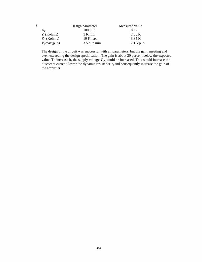
f. Design parameter Measured value AV 100 min. 80.7 Zi (Kohms) 1 Kmin. 2.38 K ZO (Kohms) 10 Kmax. 3.35 K VOmax(p−p) 3 Vp−p min. 7.1 Vp−p The design of the circuit was successful with all parameters, but the gain, meeting and
even exceeding the design specification. The gain is about 20 percent below the expected value. To increase it, the supply voltage VCC could be increased. This would increase the quiescent current, lower the dynamic resistance re and consequently increase the gain of the amplifier.
284
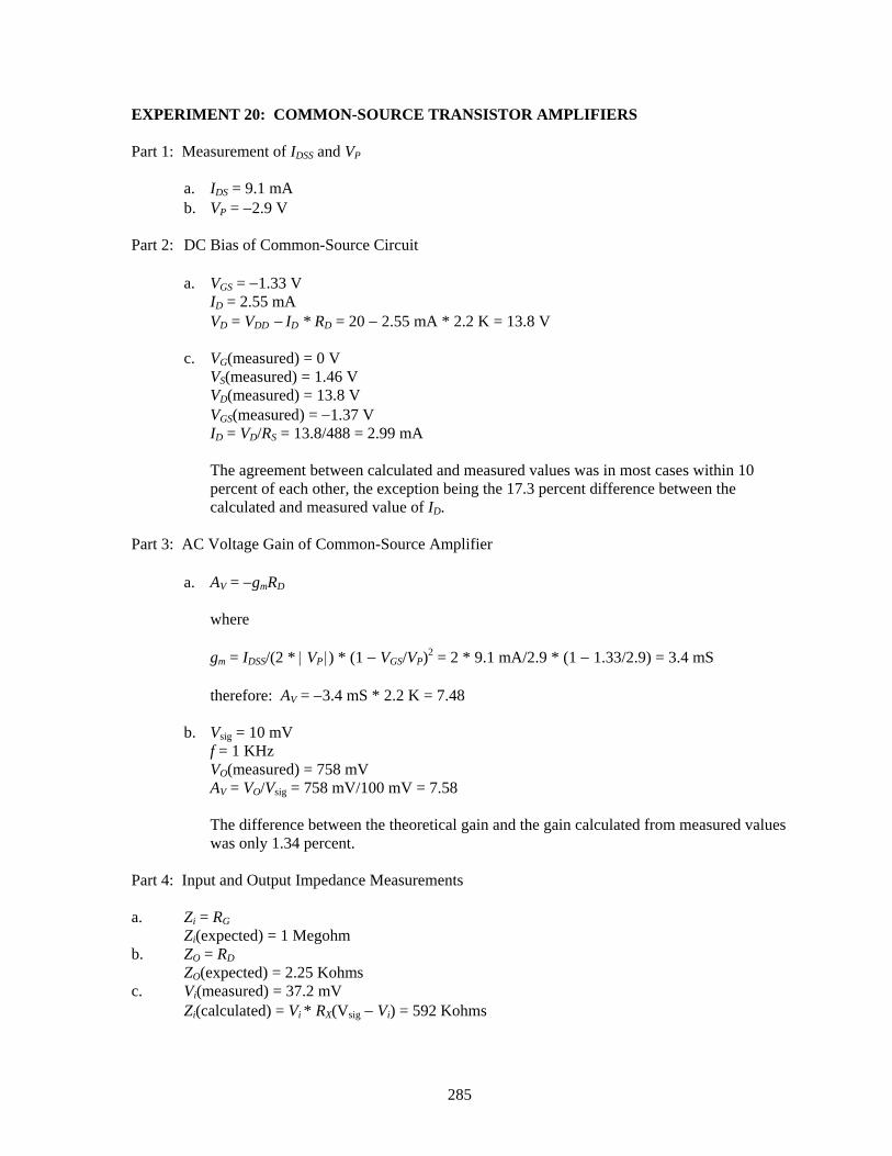
EXPERIMENT 20: COMMON-SOURCE TRANSISTOR AMPLIFIERS Part 1: Measurement of IDSS and VP a. IDS = 9.1 mA b. VP = −2.9 V Part 2: DC Bias of Common-Source Circuit a. VGS = −1.33 V ID = 2.55 mA VD = VDD − ID * RD = 20 − 2.55 mA * 2.2 K = 13.8 V c. VG(measured) = 0 V VS(measured) = 1.46 V VD(measured) = 13.8 V VGS(measured) = −1.37 V ID = VD/RS = 13.8/488 = 2.99 mA The agreement between calculated and measured values was in most cases within 10
percent of each other, the exception being the 17.3 percent difference between the calculated and measured value of ID.
Part 3: AC Voltage Gain of Common-Source Amplifier a. AV = −gmRD where gm = IDSS/(2 * | VP |) * (1 − VGS/VP)2 = 2 * 9.1 mA/2.9 * (1 − 1.33/2.9) = 3.4 mS therefore: AV = −3.4 mS * 2.2 K = 7.48 b. Vsig = 10 mV f = 1 KHz VO(measured) = 758 mV AV = VO/Vsig = 758 mV/100 mV = 7.58 The difference between the theoretical gain and the gain calculated from measured values
was only 1.34 percent. Part 4: Input and Output Impedance Measurements a. Zi = RG Zi(expected) = 1 Megohm b. ZO = RD ZO(expected) = 2.25 Kohms c. Vi(measured) = 37.2 mV Zi(calculated) = Vi * RX(Vsig − Vi) = 592 Kohms
285
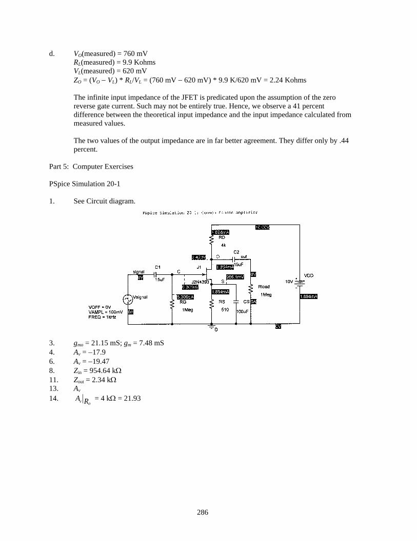
d. VO(measured) = 760 mV RL(measured) = 9.9 Kohms VL(measured) = 620 mV ZO = (VO − VL) * RL/VL = (760 mV − 620 mV) * 9.9 K/620 mV = 2.24 Kohms The infinite input impedance of the JFET is predicated upon the assumption of the zero
reverse gate current. Such may not be entirely true. Hence, we observe a 41 percent difference between the theoretical input impedance and the input impedance calculated from measured values.
The two values of the output impedance are in far better agreement. They differ only by .44
percent. Part 5: Computer Exercises PSpice Simulation 20-1 1. See Circuit diagram.
3. gmo = 21.15 mS; gm = 7.48 mS 4. Av = −17.9 6. Av = −19.47 8. Zin = 954.64 kΩ 11. Zout = 2.34 kΩ 13. Av 14.
DvA R = 4 kΩ = 21.93
286
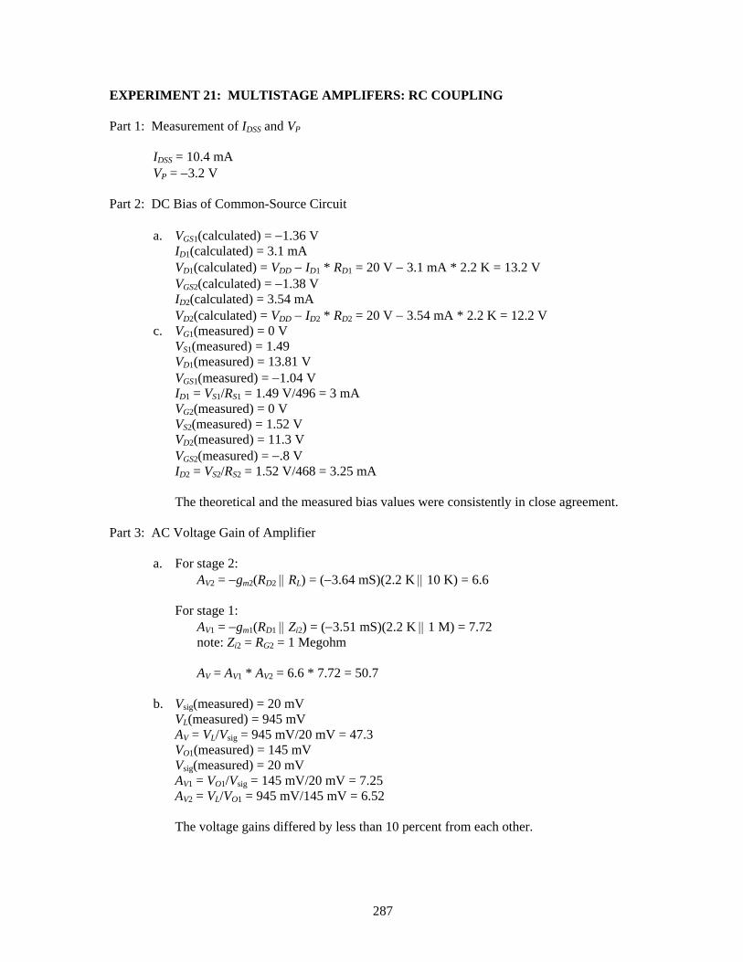
EXPERIMENT 21: MULTISTAGE AMPLIFERS: RC COUPLING Part 1: Measurement of IDSS and VP IDSS = 10.4 mA VP = −3.2 V Part 2: DC Bias of Common-Source Circuit a. VGS1(calculated) = −1.36 V ID1(calculated) = 3.1 mA VD1(calculated) = VDD − ID1 * RD1 = 20 V − 3.1 mA * 2.2 K = 13.2 V VGS2(calculated) = −1.38 V ID2(calculated) = 3.54 mA VD2(calculated) = VDD − ID2 * RD2 = 20 V − 3.54 mA * 2.2 K = 12.2 V c. VG1(measured) = 0 V VS1(measured) = 1.49 VD1(measured) = 13.81 V VGS1(measured) = −1.04 V ID1 = VS1/RS1 = 1.49 V/496 = 3 mA VG2(measured) = 0 V VS2(measured) = 1.52 V VD2(measured) = 11.3 V VGS2(measured) = −.8 V ID2 = VS2/RS2 = 1.52 V/468 = 3.25 mA The theoretical and the measured bias values were consistently in close agreement. Part 3: AC Voltage Gain of Amplifier a. For stage 2: AV2 = −gm2(RD2 || RL) = (−3.64 mS)(2.2 K || 10 K) = 6.6 For stage 1: AV1 = −gm1(RD1 || Zi2) = (−3.51 mS)(2.2 K || 1 M) = 7.72 note: Zi2 = RG2 = 1 Megohm AV = AV1 * AV2 = 6.6 * 7.72 = 50.7 b. Vsig(measured) = 20 mV VL(measured) = 945 mV AV = VL/Vsig = 945 mV/20 mV = 47.3 VO1(measured) = 145 mV Vsig(measured) = 20 mV AV1 = VO1/Vsig = 145 mV/20 mV = 7.25 AV2 = VL/VO1 = 945 mV/145 mV = 6.52 The voltage gains differed by less than 10 percent from each other.
287
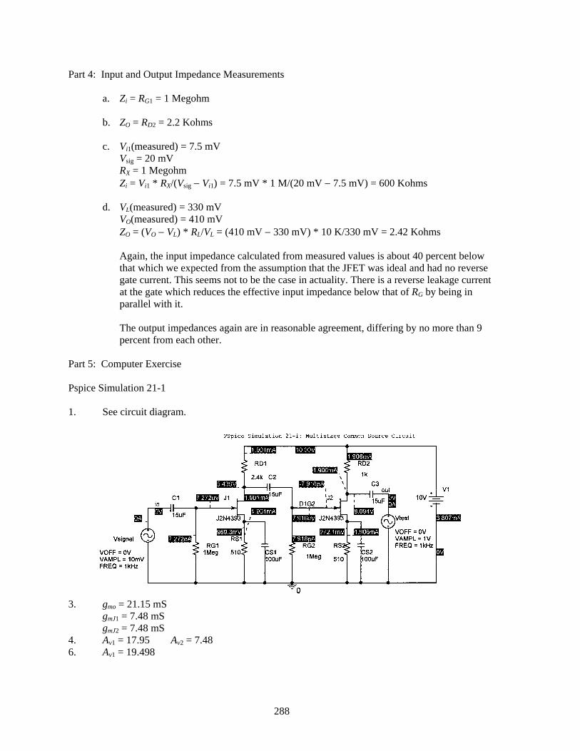
Part 4: Input and Output Impedance Measurements a. Zi = RG1 = 1 Megohm b. ZO = RD2 = 2.2 Kohms c. Vi1(measured) = 7.5 mV Vsig = 20 mV RX = 1 Megohm Zi = Vi1 * RX/(Vsig − Vi1) = 7.5 mV * 1 M/(20 mV − 7.5 mV) = 600 Kohms d. VL(measured) = 330 mV VO(measured) = 410 mV ZO = (VO − VL) * RL/VL = (410 mV − 330 mV) * 10 K/330 mV = 2.42 Kohms Again, the input impedance calculated from measured values is about 40 percent below
that which we expected from the assumption that the JFET was ideal and had no reverse gate current. This seems not to be the case in actuality. There is a reverse leakage current at the gate which reduces the effective input impedance below that of RG by being in parallel with it.
The output impedances again are in reasonable agreement, differing by no more than 9
percent from each other. Part 5: Computer Exercise Pspice Simulation 21-1 1. See circuit diagram.
3. gmo = 21.15 mS gmJ1 = 7.48 mS gmJ2 = 7.48 mS 4. Av1 = 17.95 Av2 = 7.48 6. Av1 = 19.498
288
7. Av2 = 8.275 10. (Av1)(Av2) = 161.35 11. (Av1)(Av2) = 161.35 14. Yes 16. Interchange J1 with J2 17. Zin = 956.89 kΩ 20. Zout = 989.74 Ω
289
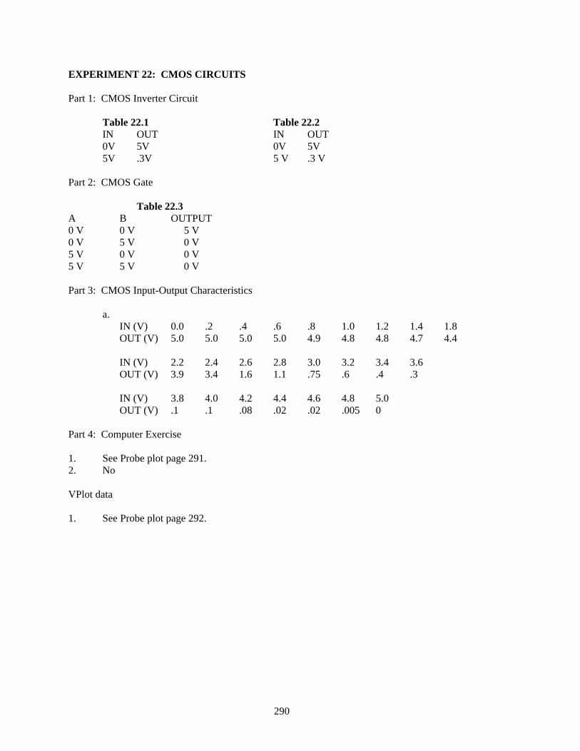
EXPERIMENT 22: CMOS CIRCUITS Part 1: CMOS Inverter Circuit Table 22.1 Table 22.2 IN OUT IN OUT 0V 5V 0V 5V 5V .3V 5 V .3 V Part 2: CMOS Gate Table 22.3 A B OUTPUT 0 V 0 V 5 V 0 V 5 V 0 V 5 V 0 V 0 V 5 V 5 V 0 V Part 3: CMOS Input-Output Characteristics a. IN (V) 0.0 .2 .4 .6 .8 1.0 1.2 1.4 1.8 OUT (V) 5.0 5.0 5.0 5.0 4.9 4.8 4.8 4.7 4.4 IN (V) 2.2 2.4 2.6 2.8 3.0 3.2 3.4 3.6 OUT (V) 3.9 3.4 1.6 1.1 .75 .6 .4 .3 IN (V) 3.8 4.0 4.2 4.4 4.6 4.8 5.0 OUT (V) .1 .1 .08 .02 .02 .005 0 Part 4: Computer Exercise 1. See Probe plot page 291. 2. No VPlot data 1. See Probe plot page 292.
290
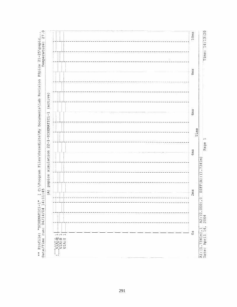
291
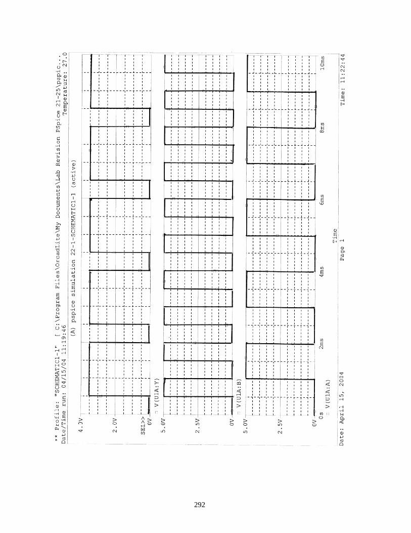
292
EXPERIMENT 23: DARLINGTON AND CASCODE AMPLIFIER CIRCUITS Part 1: Darlington Emitter-Follower Circuit a. VB(calculated) = 2.21 V B
VE(calculated) = 1.01 V AV = RE/(RE + re) = 47/(47 + 10) = .83 b. VB(measured) = 5.9 V B
VE(measured) = 4.94 V IB(calculated) = 199 μA B
IE(calculated) = 106 mA β(calculated) = 106 mA/199 μA = 535 c. Vi(measured) = 350 mV VO(measured) = 340 mV AV = VO/Vi = 340 mV/350 mV = .97 Part 2: Darlington Input and Output Impedance a. Zi(calculated) = 20.6 K || (535 * 47) = 11.3 Kohms ZO = re + (RG || RB)/β = 9 ohms B
b. Vsig = 500 mV Vi(measured) = 55.6 mV Zi = [Vi/(Vsig − Vi) * Rx = [55.6 mV/(500 mV − 55.6 mV)] * 100 K = 12.5 Kohms c. VO(measured) = 492 mV VL(measured) = 476 mV RL = 100 ohms ZO = [(VO − VL)/VL] * RL = [(492 mV − 476 mV)/476 mV] * 100 = 4.2 ohms The two values of the input impedance differed by about 10.6 percent while the two
values of the output impedance differed by 53 percent. It is to be noted however that with such small values the difference in just one ohm manifests itself as a large percent change. Given the tolerances of electronic circuit due to their components and that of the Darlington chip, the results are quite satisfactory.
Part 3: Cascode Circuit a. VB1 (calculated) = 5.5 V VE1 (calculated) = 4.8 V VC1 (calculated) = 11 V VB2 (calculated) = 12 V VE2 (calculated) = 11.3 V VC2 (calculated) = 12.5 V IE1 = VE1/RE1 = 4.8 V/1 k = 4.8 mA IE2 = 11.3/1.8 K = 6.24 mA re1 = 26 mV/IE1 = 26 mV/4.8 mA = 5.4 ohms re2 = 26 mV/IE2 = 26 mV/6.24 mA = 4.2 ohms b. VB1 (measured) = 4.69 V VE1 (measured) = 4.0 V
293
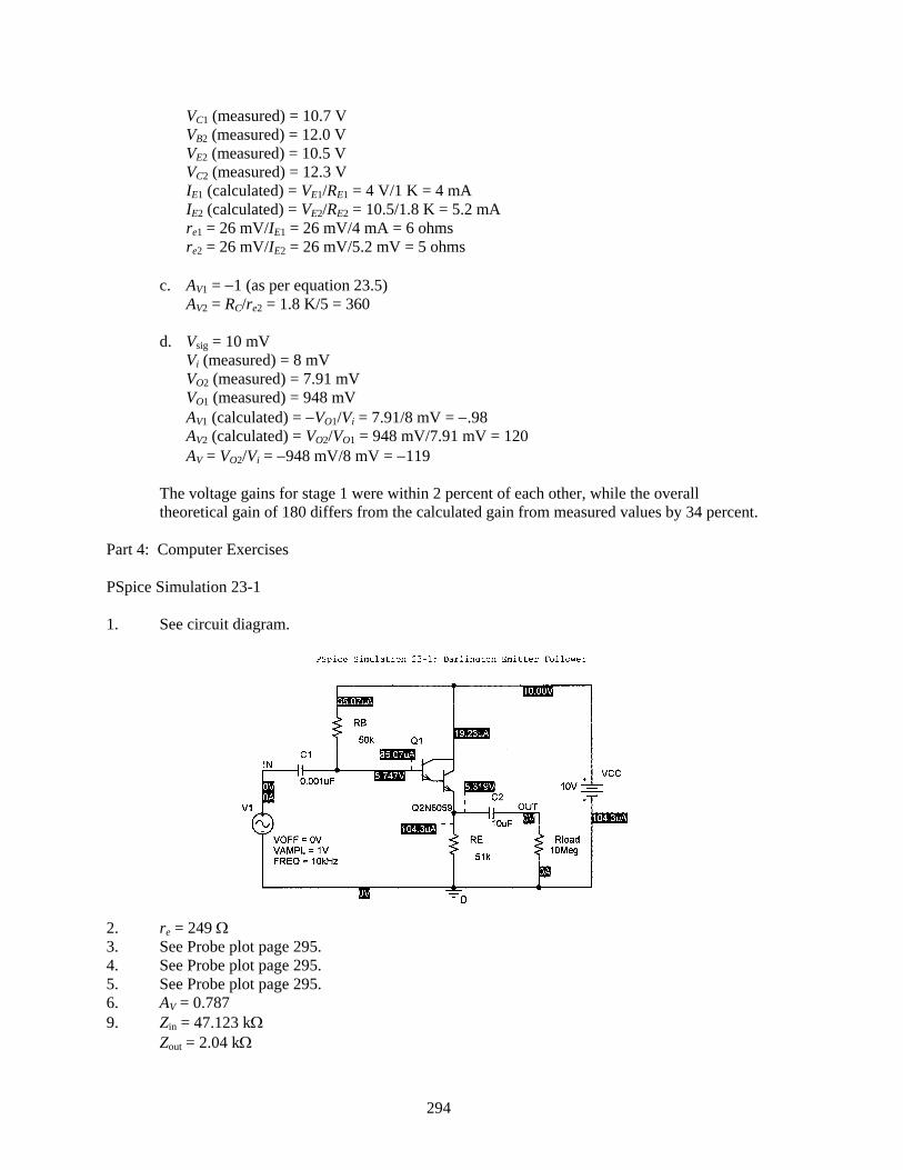
VC1 (measured) = 10.7 V VB2 (measured) = 12.0 V VE2 (measured) = 10.5 V VC2 (measured) = 12.3 V IE1 (calculated) = VE1/RE1 = 4 V/1 K = 4 mA IE2 (calculated) = VE2/RE2 = 10.5/1.8 K = 5.2 mA re1 = 26 mV/IE1 = 26 mV/4 mA = 6 ohms re2 = 26 mV/IE2 = 26 mV/5.2 mV = 5 ohms c. AV1 = −1 (as per equation 23.5) AV2 = RC/re2 = 1.8 K/5 = 360 d. Vsig = 10 mV Vi (measured) = 8 mV VO2 (measured) = 7.91 mV VO1 (measured) = 948 mV AV1 (calculated) = −VO1/Vi = 7.91/8 mV = −.98 AV2 (calculated) = VO2/VO1 = 948 mV/7.91 mV = 120 AV = VO2/Vi = −948 mV/8 mV = −119 The voltage gains for stage 1 were within 2 percent of each other, while the overall
theoretical gain of 180 differs from the calculated gain from measured values by 34 percent. Part 4: Computer Exercises PSpice Simulation 23-1 1. See circuit diagram.
2. re = 249 Ω 3. See Probe plot page 295. 4. See Probe plot page 295. 5. See Probe plot page 295. 6. AV = 0.787 9. Zin = 47.123 kΩ Zout = 2.04 kΩ
294
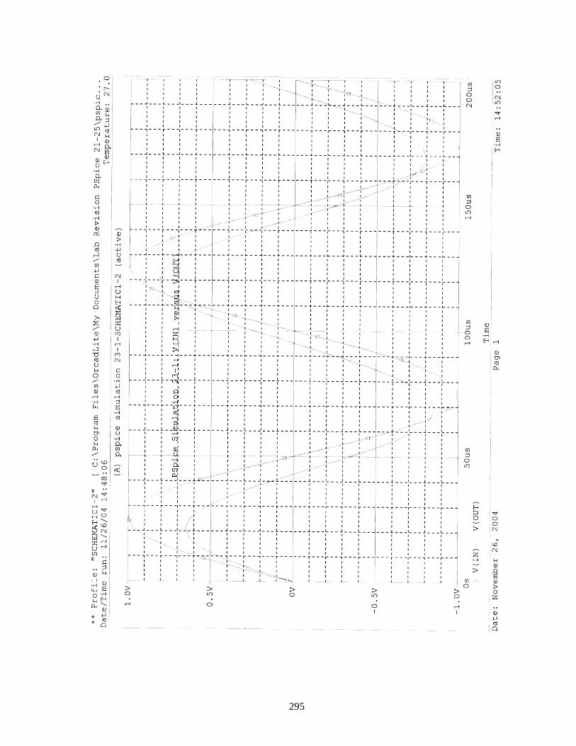
295
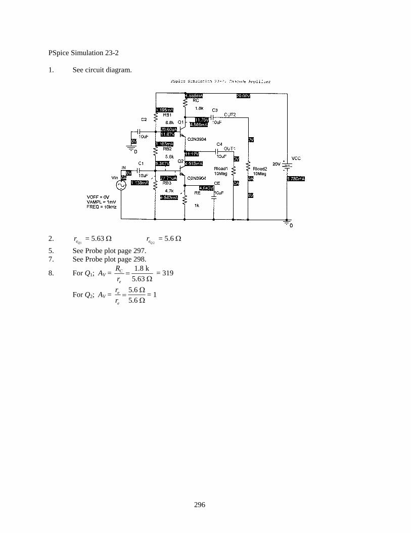
PSpice Simulation 23-2 1. See circuit diagram.
2. = 5.63 Ω = 5.6 Ω
1Qer 2Qer
5. See Probe plot page 297. 7. See Probe plot page 298.
8. For Q1; AV = 1.8 k5.63
C
e
Rr
=Ω
= 319
For Q2; AV = 5.6 5.6
e
e
rr
Ω=
Ω= 1
296
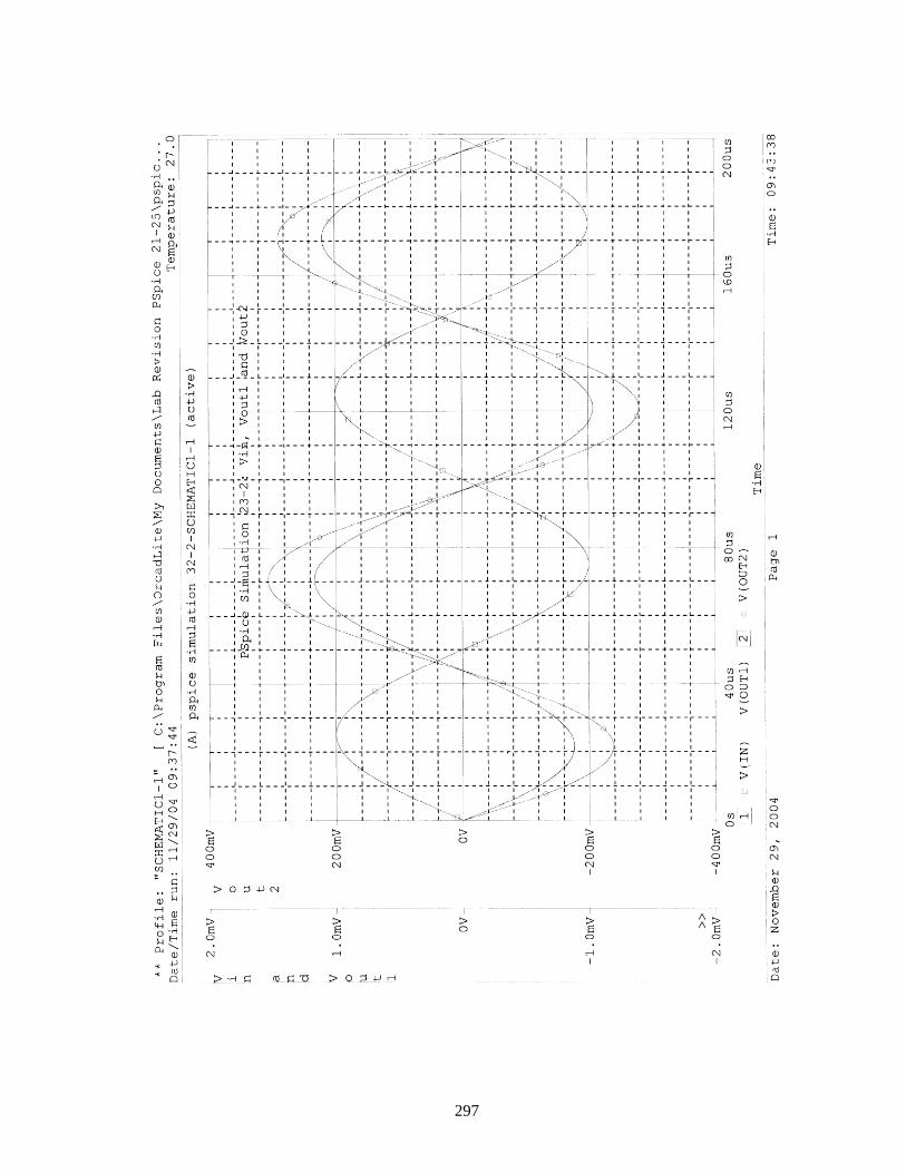
297
298
EXPERIMENT 24: CURRENT SOURCE AND CURRENT MIRROR CIRCUITS Part 1: JFET Current Source a. VDS (measured) = 9.64 V b. IL = (VDD − VDS)/RL = (10 − 9.64)/51.2 = 7.03 mA c. Table 24.1 RL (ohms) 20 51 82 100 150 VDS (Volts) 9.88 9.64 9.44 9.34 8.85 IL (mA) 6.1 7.03 6.83 6.60 7.57 Part 2: BJT Current Source a. IL = 1.9 mA b. VE (measured) = −.68 V VC (measured) = .404 V c. IE (calculated) = 2.13 mA IL (calculated) = 1.88 mA d. Table 24.2 RL (kohms) 3.6 4.3 5.1 VE (Volts) −.68 −.67 −.68 VC (Volts) 3.03 1.74 .404 IE (mA) 2.14 2.17 2.13 IL (mA) 1.94 1.92 1.88 Part 3: Current Mirror a. IX = .9 mA b. VB1 = .669 V VC2 = 2.24 V IX = .89 mA IL = 1.0 mA c. IX (calculated) = 1 mA VB1 (measured) = .669 V VC2 (measured) = 4.1 V IX = .9 mA IL = 1.5 mA
299
Part 4: Multiple Current Mirrors a. IX (calculated) = 1 mA b. VB1 (measured) = .672 V VC2 (measured) = 1.67 V VC3 (measured) = 1.65 V IX = 1.01 mA IL1 = 1.58 mA IL2 = 1.78 mA c. IX (calculated) = 1 mA VB1 (measured) = .672 V VC2 (measured) = 3.81 V VC3 (measured) = 2.87 V IX = 1.02 mA IL1 = 1.73 mA IL2 = 1.44 mA Part 5: Computer Exercise PSpice Simulation 24-1 1. See circuit diagram.
2. I(RX) = 933.6 μA I(RL) = 1.020 mA 3. Yes
300
4. See Circuit diagram.
5. I(RX) = 933.6 μA I(RL) = 991.3 μA 6. Yes 8. Yes 10. Yes 11. No 12. Yes
301
EXPERIMENT 25: FREQUENCY RESPONSE OF COMMON-EMITTER AMPLIFIERS Résumé fL,1 = 1/(2 * 3.24 * 1.39 K * 10 μf) = 11.5 Hz fL,2 = 1/(2 * 3.24 * 6.1 K * 1 μf) = 26 Hz fL,E = 1/(2 * 3.14 * 2.2 K * 20 μf) = 3.62 Hz fH,i = 1/(2 * 3.14 * 1.68 K * 960 μf) = 98.7 KHz fH,O = 1/(2 * 3.14 * 1.43 K * 45 pf) = 2.43 MHz Part 1: Low-Frequency Response Calculations a. Cbe (specified) = 100 pf Cbc (specified) = 10 pf Cce (specified) = 15 pf CW,i (approximated) = 20 pf CW,o (approximated) = 30 pf b. β(measured) = 126 c. VB (calculated) = 4.08 V B
VE (calculated) = 3.38 V VC (calculated) = 14 V IE (calculated) = 1.54 mA re = 26 mV/IE = 26 mV/1.54 mA = 16.9 ohms d. AV (mid) = (RC || RL)/re = (3.9 K || 2.2 K)/16.9 = 83.2 e. fL,1 (calculated) = 11.5 Hz fL,2 (calculated) = 26.2 Hz fL,E (calculated) = 3.62 Hz Part 2: Low Frequency Response Measurements b. Vsig (measured) = 30 mV VO (measured) = 2.1 V AV (mid) = 70
Table 25.1 f (Hz) 50 100 200 400 600 800 1 K 2 K 3 K 5 K 10 KVO(p−p) .4 .5 .9 1.6 1.8 1.9 2.0 2.1 2.1 2.1 2.2
Table 25.2
f (Hz) 50 100 200 400 600 800 1 K 2 K 3 K 5 K 10 KAV 13.2 16.7 30 53.3 60 63.3 66.7 70 70 70 73.3
Part 3: High Frequency Response Calculations a. fH,I (calculated) = 98.7 KHz fH,O (calculated) = 2.47 MHz
302
b. Table 25.3 f (KHz) 10 50 100 300 500 600 700 900 1000 2000VO(p−p) 2.2 2.2 2.1 1.9 1.6 1.5 1.4 1.3 1.3 .8
Table 25.4
f (KHz) 10 50 100 300 500 600 700 900 1000 2000AV 73 73 70 63 53 20 46 40 40 27
Part 4: Plotting Bode Plot and Frequency Response
Fig 25.2
from plot: f1 = 400 Hz f2 = 500 Hz Part 5: Computer Exercise PSpice Simulation 25-1 1. See circuit diagram.
2. re = 17.2 Ω; AV mid = 81.3 4. See Probe plot 346. 5. Almost identical 6. See Probe plot page 346. 7. See Probe plot page 347. 8. 20 log(78.028) = 37.84 both gains agree
303
304
305
EXPERIMENT 26: CLASS A AND CLASS B POWER AMPLIFIERS Part 1: Class A Amplifier: DC Bias a. VB (calculated) = 1.53 V B
VE (calculated) = .83 V IE (calculated) = IC = VE/RE = .83/20 = 41 mA VC (calculated) = 5.1 V b. VB (measured) = 1.59 V B
VE (measured) = .88 V VC (measured) = 5.3 V IE (calculated) = IC = VE/RE = .88/20 = 44 mA Part 2: Class-A Amplifier: AC Operation a. Pi (calculated) = 400 mW VO (calculated) = 5.3 Vp−p PO (calculated) = 29.3 mW % efficiency (calculated) = 7.3 percent b. Vi (measured) = 65 mV Vo (measured) = 5 Vp−p c. Pi = 400 mW PO = 26 mW % efficiency (calculated) = 6.5 percent While the values for the power and the efficiency are fairly consistent between the
theoretical and those calculated from measured values, the low efficiency of the amplifier is an undesirable feature. In general, Class A amplifiers operate close to a 25 percent efficiency. This circuit would need to be redesigned to make it a practical circuit.
d. Vi (measured) = 32.5 mVp−p VO (measured) = 3 Vp−p e. Pi (calculated) = 400 mW PO (calculated) = 9.38 mW % efficiency (calculated) = 2.3 percent f. Pi = 400 mW PO = 93 mW % efficiency = 2.3 percent As stated previously, while the data is consistent, the values of the efficiency makes this
not a practical circuit.
306
Part 3: Class-B Amplifier Operation a. for VO = 1 Vpeak Pi (calculated) = 1.59 W PO (calculated) = 50 mW % efficiency (calculated) = 3.1 percent for VO = 2 Vpeak Pi = 1.59 W PO = 200 mW % efficiency (calculated) = 12.6 percent b. Vi (measured) = 2.9 Vp−p VO (measured) = 2.7 Vp−p Pi = 890 mW PO = 91 mW % efficiency = 10.2% c. Vi (measured) = 5 Vp−p VO (measured) = 4 Vp−p Idc (measured) = 159 mA Pi = 1.27 W PO = 637 mW % efficiency = 50.2% Note that the efficiency of the Class B amplifier increases with increasing input signal
and consequent increasing output signal. Also observe that the two stages of the Class B amplifier shown in Figure 26.2 are in the emitter follower configuration. Thus, the voltage gain for each stage is near unity. This is what the data of the input and the output voltages show. Note also, that as the output voltage approaches its maximum value that the efficiency of the device approaches its theoretical efficiency of about 78 percent.
Part 4: Computer Exercises PSpice Simulation 26-1 1. See Circuit diagram.
307
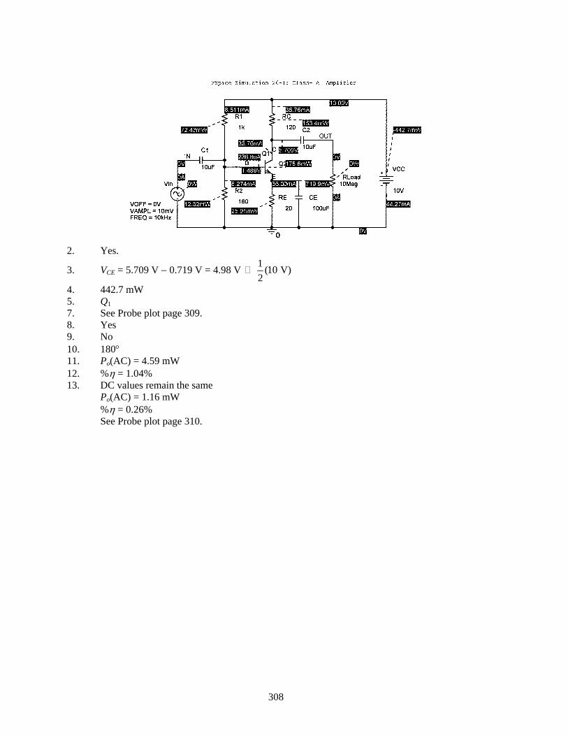
2. Yes.
3. VCE = 5.709 V − 0.719 V = 4.98 V 1 (10 V)2
4. 442.7 mW 5. Q17. See Probe plot page 309. 8. Yes 9. No 10. 180° 11. Po(AC) = 4.59 mW 12. %η = 1.04% 13. DC values remain the same Po(AC) = 1.16 mW %η = 0.26% See Probe plot page 310.
308
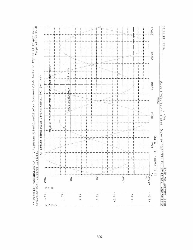
309
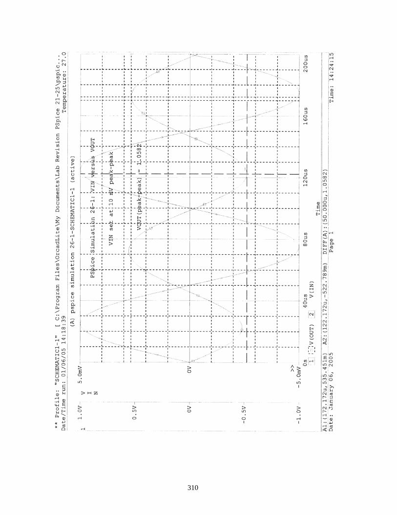
310
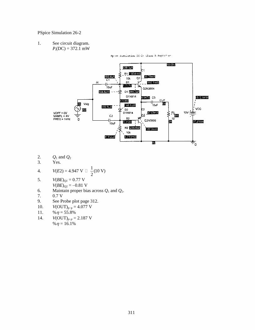
PSpice Simulation 26-2 1. See circuit diagram. Pi(DC) = 372.1 mW
2. Q1 and Q23. Yes.
4. V(E2) = 4.947 V 1 (10 V)2
5. V(BE)Q1 = 0.77 V V(BE)Q2 = −0.81 V 6. Maintain proper bias across Q1 and Q2. 7. 0.7 V 9. See Probe plot page 312. 10. V(OUT)p−p = 4.077 V 11. %η = 55.8% 14. V(OUT)p−p = 2.187 V %η = 16.1%
311
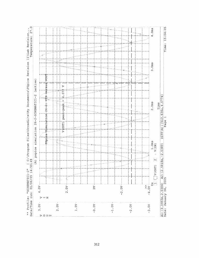
312
EXPERIMENT 27: DIFFERENTIAL AMPLIFIER CIRCUITS Part 1: DC Bias of BJT Differential Amplifier a. VB (calculated) = 0V B
VE (calculated) = −.7 V VC (calculated) = 5.43 V IE (calculated) = 457 μA re (calculated) = 57 ohms b. Q1 Q2 VB (measured) −.10 V 0 V B
VE (measured) −.65 V −.65 V VC (measured) 5.10 V 4.9 V IE (calculated) 490 μA 510 μA re 53 ohms 51 ohms Part 2: AC Operation of BJT Differential Amplifier a. AV,d (calculated) = 179 AV,c (calculated) = .5 b. VO1 (measured) = 1.48 V VO2 (measured) = 1.43 V VO,d = (VO,1 + VO,2)/2 = (1.48 + 1.43)/2 = 1.46 V AV,d = VO,d/Vi = 72.8 c. VO,c (measured) = .55 V AV,c = VO,c/Vi = .55 Part 3: DC Bias of BJT Differential Amplifier with Current Source a. For either Q1 or Q2: VB (calculated) = 0 V B
VE (calculated) = −.7 V VC (calculated) = 9 V IE (calculated) = .5 mA re (calculated) = 52 ohms For Q3: VB (calculated) = −5 V B
VE (calculated) = −5.7 V VC (calculated) = −.7 V IE (calculated) = 1 mA re (calculated) = 26 ohms
313
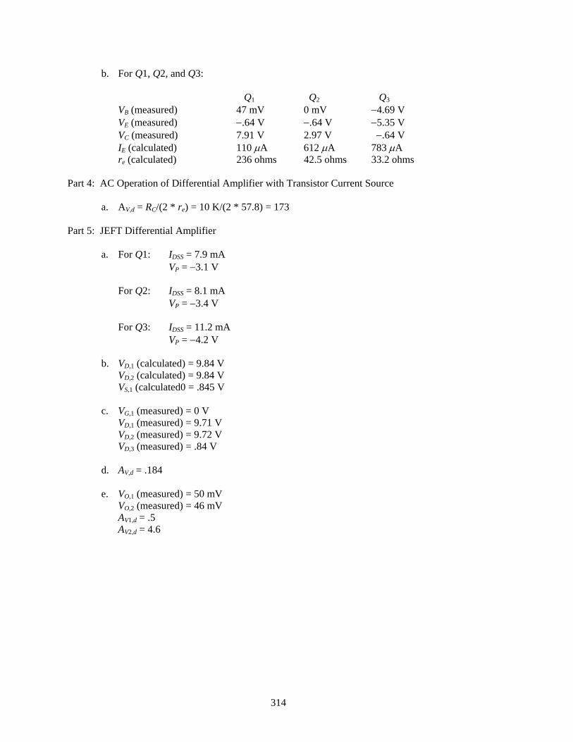
b. For Q1, Q2, and Q3: Q1 Q2 Q3
VB (measured) 47 mV 0 mV −4.69 V B
VE (measured) −.64 V −.64 V −5.35 V VC (measured) 7.91 V 2.97 V −.64 V IE (calculated) 110 μA 612 μA 783 μA re (calculated) 236 ohms 42.5 ohms 33.2 ohms Part 4: AC Operation of Differential Amplifier with Transistor Current Source a. AV,d = RC/(2 * re) = 10 K/(2 * 57.8) = 173 Part 5: JEFT Differential Amplifier a. For Q1: IDSS = 7.9 mA VP = −3.1 V For Q2: IDSS = 8.1 mA VP = −3.4 V For Q3: IDSS = 11.2 mA VP = −4.2 V b. VD,1 (calculated) = 9.84 V VD,2 (calculated) = 9.84 V VS,1 (calculated0 = .845 V c. VG,1 (measured) = 0 V VD,1 (measured) = 9.71 V VD,2 (measured) = 9.72 V VD,3 (measured) = .84 V d. AV,d = .184 e. VO,1 (measured) = 50 mV VO,2 (measured) = 46 mV AV1,d = .5 AV2,d = 4.6
314
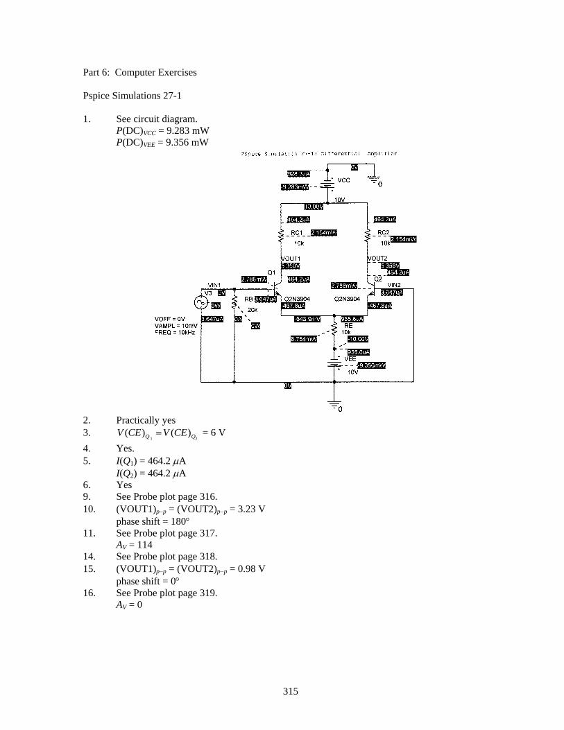
Part 6: Computer Exercises Pspice Simulations 27-1 1. See circuit diagram. P(DC)VCC = 9.283 mW P(DC)VEE = 9.356 mW
2. Practically yes 3. = 6 V
1 2( ) ( )Q QV CE V CE=
4. Yes. 5. I(Q1) = 464.2 μA I(Q2) = 464.2 μA 6. Yes 9. See Probe plot page 316. 10. (VOUT1)p−p = (VOUT2)p−p = 3.23 V phase shift = 180° 11. See Probe plot page 317. AV = 114 14. See Probe plot page 318. 15. (VOUT1)p−p = (VOUT2)p−p = 0.98 V phase shift = 0° 16. See Probe plot page 319. AV = 0
315
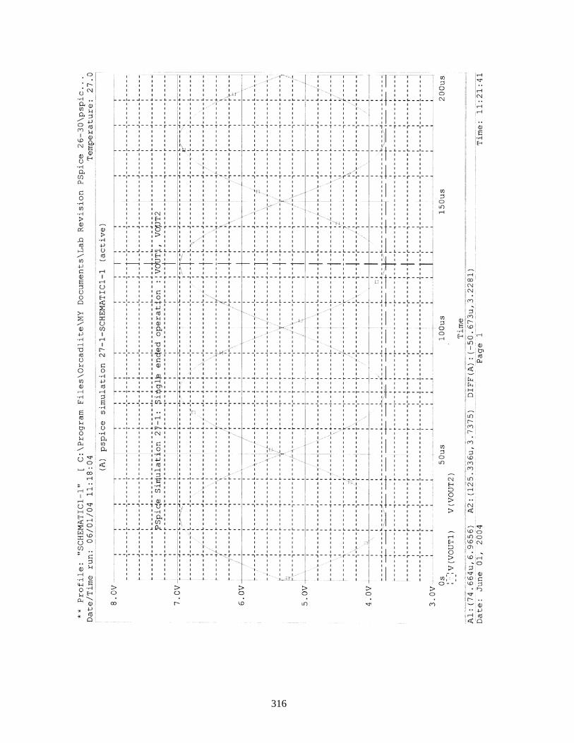
316
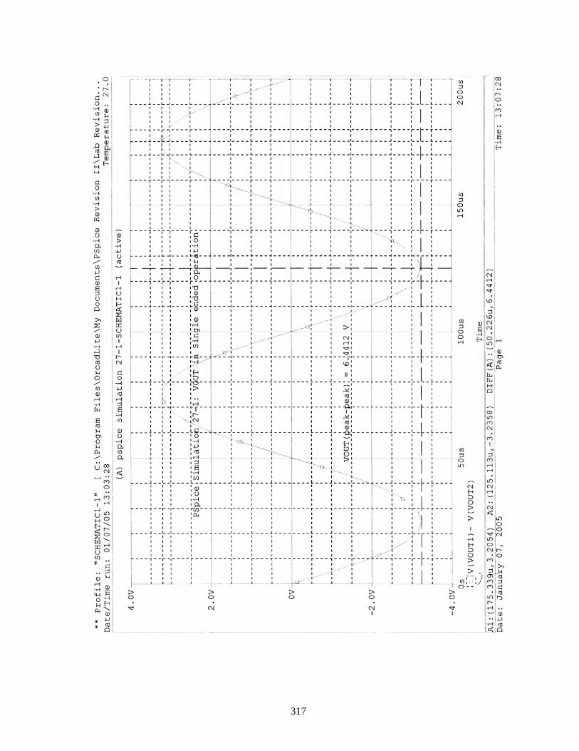
317
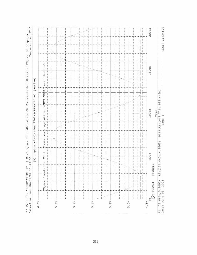
318
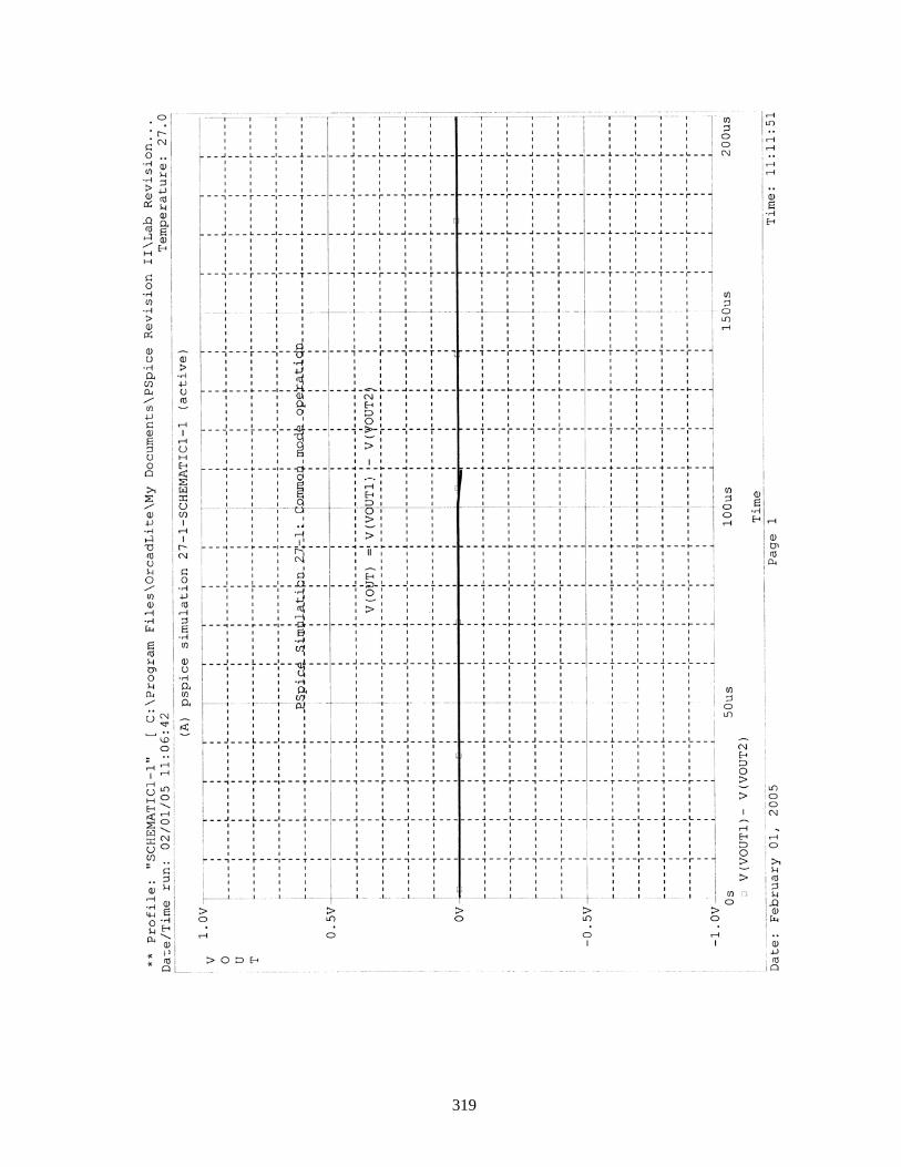
319
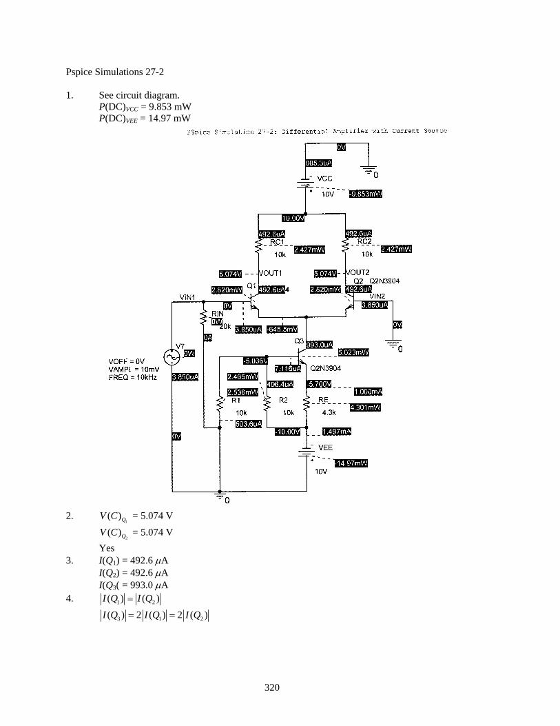
Pspice Simulations 27-2 1. See circuit diagram. P(DC)VCC = 9.853 mW P(DC)VEE = 14.97 mW
2. = 5.074 V
1( )QV C
= 5.074 V 2
( )QV C Yes 3. I(Q1) = 492.6 μA I(Q2) = 492.6 μA I(Q3( = 993.0 μA 4. 1 2( ) ( )I Q I Q= 3 1( ) 2 ( ) 2 ( )I Q I Q I Q= = 2
320
7. See Probe plot page 322. 8. Both voltages are 1.7602 Vp−p
phase shift = 180° 9. See Probe plot page 323. AV = 125 12. See Probe plot page 324. 13. 1.6 mVp−p phase shift = 0° 14. See probe plot page 325. AV = 0
321
322 322
323
324
325
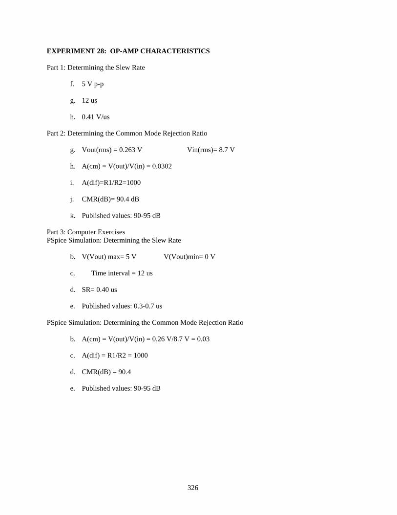
EXPERIMENT 28: OP-AMP CHARACTERISTICS Part 1: Determining the Slew Rate
f. 5 V p-p g. 12 us h. 0.41 V/us
Part 2: Determining the Common Mode Rejection Ratio
g. Vout(rms) = 0.263 V Vin(rms)= 8.7 V h. A(cm) = V(out)/V(in) = 0.0302 i. A(dif)=R1/R2=1000 j. CMR(dB)= 90.4 dB k. Published values: 90-95 dB
Part 3: Computer Exercises PSpice Simulation: Determining the Slew Rate
b. V(Vout) max= 5 V V(Vout)min= 0 V c. Time interval = 12 us d. SR= 0.40 us e. Published values: 0.3-0.7 us
PSpice Simulation: Determining the Common Mode Rejection Ratio
b. A(cm) = V(out)/V(in) = 0.26 V/8.7 V = 0.03 c. A(dif) = R1/R2 = 1000 d. CMR(dB) = 90.4 e. Published values: 90-95 dB
326
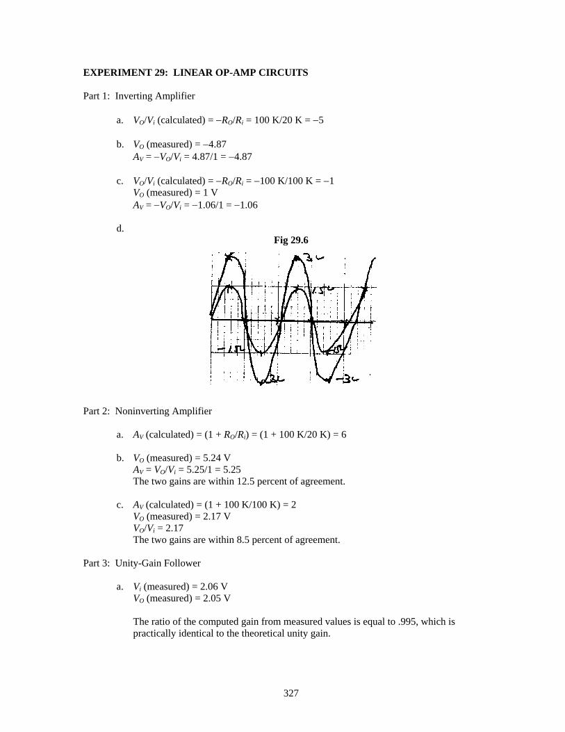
EXPERIMENT 29: LINEAR OP-AMP CIRCUITS Part 1: Inverting Amplifier a. VO/Vi (calculated) = −RO/Ri = 100 K/20 K = −5 b. VO (measured) = −4.87 AV = −VO/Vi = 4.87/1 = −4.87 c. VO/Vi (calculated) = −RO/Ri = −100 K/100 K = −1 VO (measured) = 1 V AV = −VO/Vi = −1.06/1 = −1.06 d.
Fig 29.6
Part 2: Noninverting Amplifier a. AV (calculated) = (1 + RO/Ri) = (1 + 100 K/20 K) = 6 b. VO (measured) = 5.24 V AV = VO/Vi = 5.25/1 = 5.25 The two gains are within 12.5 percent of agreement. c. AV (calculated) = (1 + 100 K/100 K) = 2 VO (measured) = 2.17 V VO/Vi = 2.17 The two gains are within 8.5 percent of agreement. Part 3: Unity-Gain Follower a. Vi (measured) = 2.06 V VO (measured) = 2.05 V The ratio of the computed gain from measured values is equal to .995, which is
practically identical to the theoretical unity gain.
327
Part 4: Summing Amplifier a. VO (calculated) = −[100 K/100 K * 1 + 100 K/20 K * 1] = −6 V b. VO (measured) = −5.02 V The difference between the two values of VO is equal to 16.3 percent. c. VO (calculated) = −[100 K/100 K * 1 + 100 K/100 K*1] = −2 V VO (measured) = −2.01 V The difference between the two values of VO is equal to .5 percent. Part 5: Computer Exercises PSpice Simulation 29-1 1. See Probe plot page 329. 2. (VOUT)peak = 5 V (VIN)peak = 1 V
3. AV = out
in in
oV RV R
= − = −5
4. VOUT 5 VVIN 1 V
= − = −5
5. Yes 6. 180° 7. Yes
328
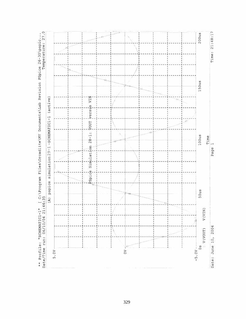
29-1
329
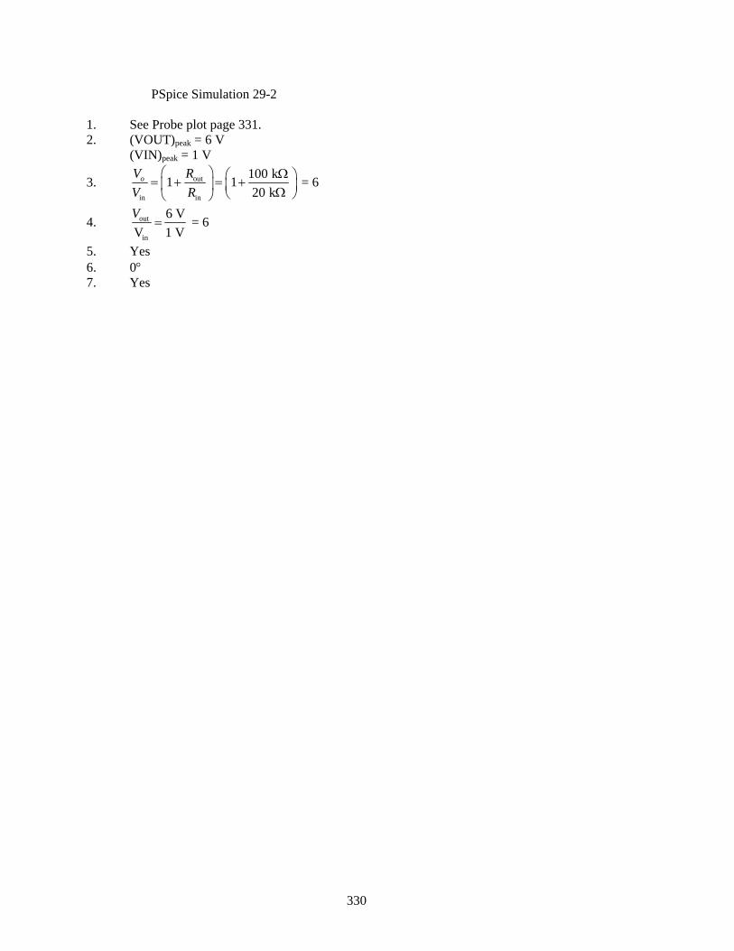
PSpice Simulation 29-2 1. See Probe plot page 331. 2. (VOUT)peak = 6 V (VIN)peak = 1 V
3. out
in in
100 k1 120 k
oV RV R
⎛ ⎞ Ω⎛ ⎞= + = +⎜ ⎟ ⎜ ⎟Ω⎝ ⎠⎝ ⎠ = 6
4. out
in
6 VV 1 VV
= = 6
5. Yes 6. 0° 7. Yes
330
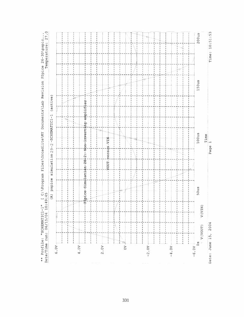
29-2
331
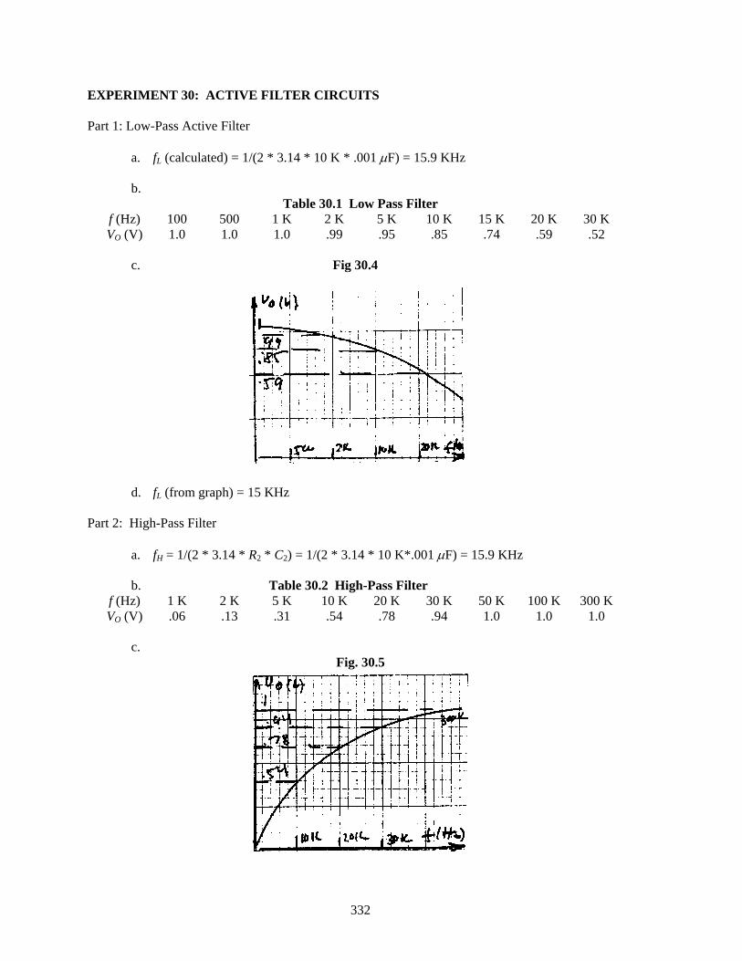
EXPERIMENT 30: ACTIVE FILTER CIRCUITS Part 1: Low-Pass Active Filter a. fL (calculated) = 1/(2 * 3.14 * 10 K * .001 μF) = 15.9 KHz b.
Table 30.1 Low Pass Filter f (Hz) 100 500 1 K 2 K 5 K 10 K 15 K 20 K 30 K VO (V) 1.0 1.0 1.0 .99 .95 .85 .74 .59 .52
c. Fig 30.4
d. fL (from graph) = 15 KHz Part 2: High-Pass Filter a. fH = 1/(2 * 3.14 * R2 * C2) = 1/(2 * 3.14 * 10 K*.001 μF) = 15.9 KHz b. Table 30.2 High-Pass Filter
f (Hz) 1 K 2 K 5 K 10 K 20 K 30 K 50 K 100 K 300 K VO (V) .06 .13 .31 .54 .78 .94 1.0 1.0 1.0
c.
Fig. 30.5
332
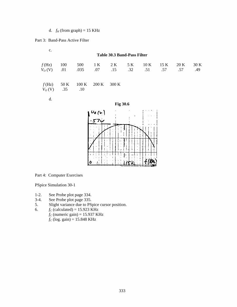
d. fH (from graph) = 15 KHz Part 3: Band-Pass Active Filter c.
Table 30.3 Band-Pass Filter
f (Hz) 100 500 1 K 2 K 5 K 10 K 15 K 20 K 30 K VO (V) .01 .035 .07 .15 .32 .51 .57 .57 .49
f (Hz) 50 K 100 K 200 K 300 K VO (V) .35 .10
d.
Fig 30.6
Part 4: Computer Exercises PSpice Simulation 30-1 1-2. See Probe plot page 334. 3-4. See Probe plot page 335. 5. Slight variance due to PSpice cursor position. 6. fC (calculated) = 15.923 KHz fC (numeric gain) = 15.937 KHz fC (log. gain) = 15.848 KHz
333
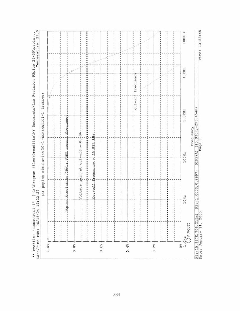
30-1
334
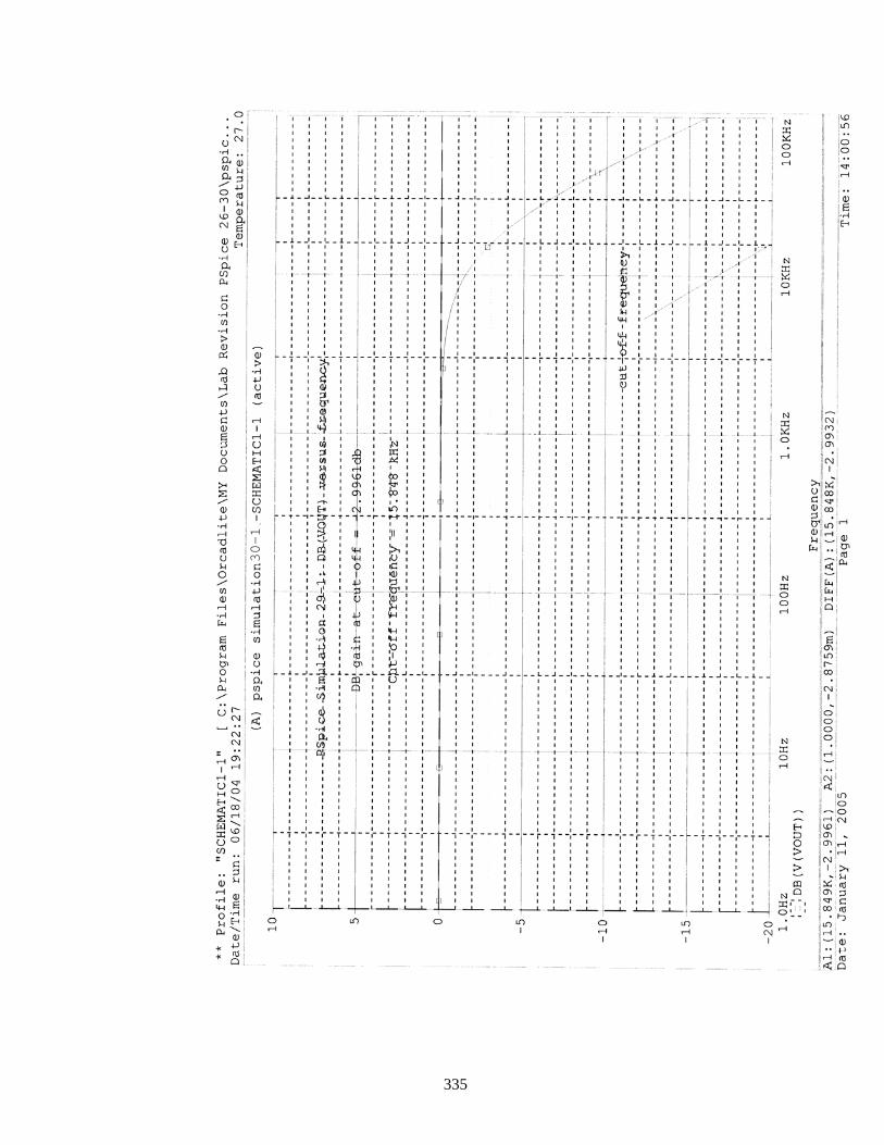
30-1
335
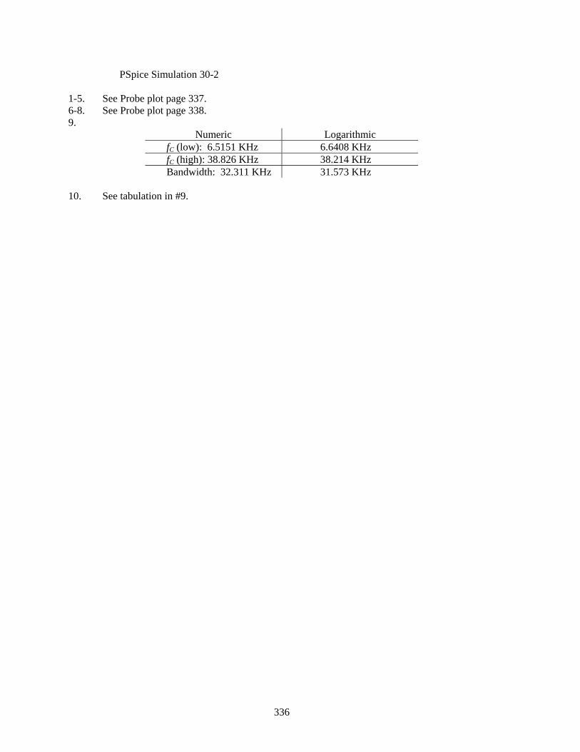
PSpice Simulation 30-2 1-5. See Probe plot page 337. 6-8. See Probe plot page 338. 9.
Numeric Logarithmic fC (low): 6.5151 KHz 6.6408 KHz fC (high): 38.826 KHz 38.214 KHz Bandwidth: 32.311 KHz 31.573 KHz
10. See tabulation in #9.
336
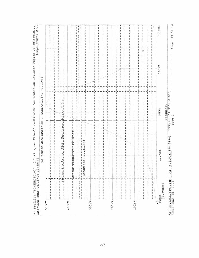
30-2
337
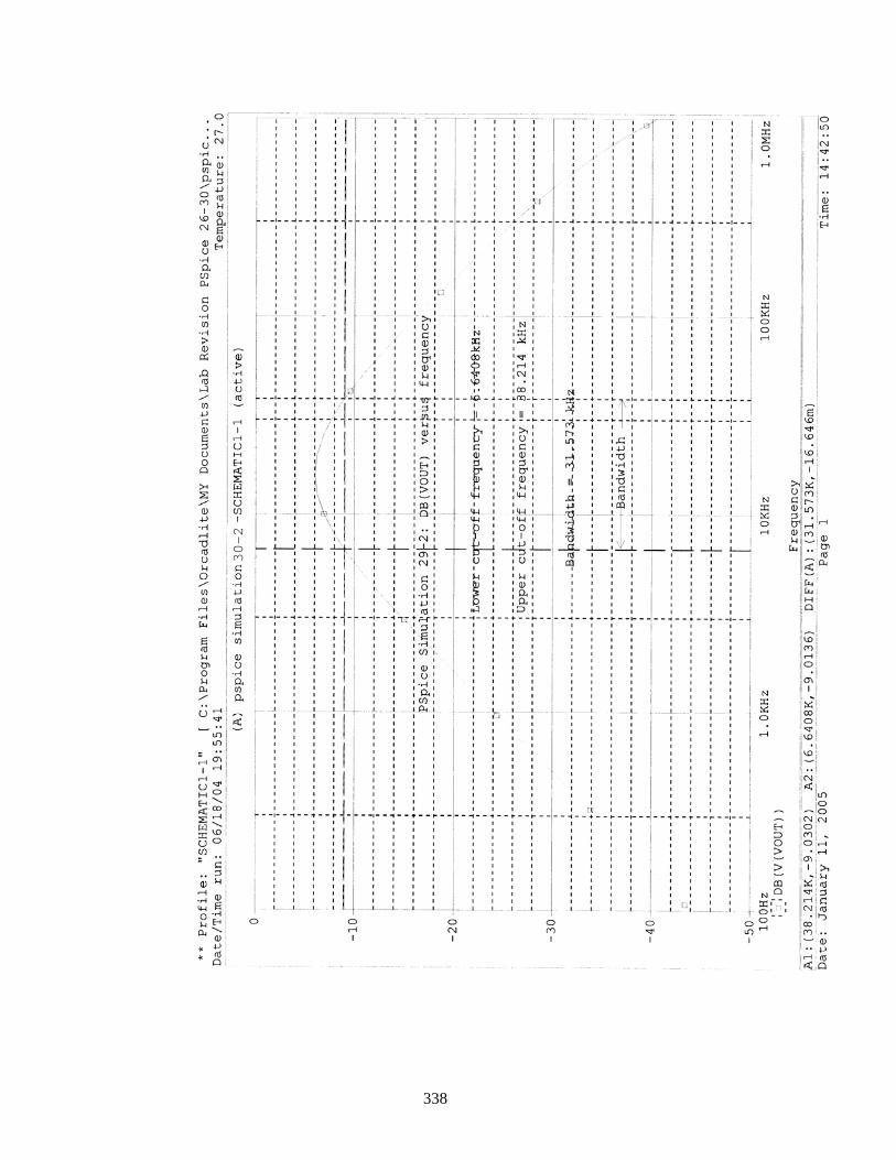
30-2
338
EXPERIMENT 31: COMPARATOR CIRCUITS OPERATION Part 1: Comparator with 74IC Used as a Level Detector a. R3 = 10 Kohms, Vref = 5 V R3 = 20 Kohms, Vref = 6.7 V c. Vref (measured) = 4.97 V d. Vi (measured) (LED goes on) = 5.01 V Vi (measured) (LED goes off) = 4.98 V e. Vref (measured) = 6.63 V Vi (measured) (LED goes on) = 6.65 V Vi (mesasured) (LED goes off) = 6.61 V All values of voltages measured and calculated relative to a particular R3 are in very close
agreement. Part 2: Comparator IC Used as a Level Detector a. R3 = 10 Kohms Vref (calculated) = 4.98 V R3 = 20 Kohms Vref (calculated) = 6.63 V c. Vref (measured) = 4.97 V (R3 = 10 Kohms) d. Vi (measured) (LED goes on) = 5.01 V Vi (measured) (LED goes off) = 4.97 V e. Replace R1 with 20 Kohm resistor. Vref (measured) = 6.67 (R3 = 20 Kohms) Vi (measured) (LED goes on) = 6.69 V Vi (measured) (LED) goes off) = 6.65 V f. Vi (measured) (LED goes on) = 6.65 V Vi (measured) (LED goes off) = 6.67 V The agreement between calculated and measured values in every case was near perfect. Part 3: Window Comparator a. V+(pin5, calculated) = 7.5 V V− (pin6, calculated) = 2.5 V c. Vi (pin1, measured) = 7.6 V V+ (pin5, measured) = 7.36 V V− (pin6, measured) = 2.3 V d. Vi (measured) (LED goes on) = 7.6 V Vi (measured) (LED goes off) = 2.6 V
339
e. Vi (measured) (LED goes on) = 7.46 V Vi (measured) (LED goes off) = 2.2 V f. Vi (measured) (LED goes on) = 7.46 V Vi (measured) (LED goes off) = 5.01 V Again as in the previous case, the agreement between measured and calculated values
was excellent. Part 4: Computer Exercises PSpice Simulation 31-1 1. See circuit diagram.
31-1:
2. Vin = 6 V; Vref = 5 V 3. Yes. I(D1) = 9.006 mA
340
4-6. See circuit diagram.
31-1:
8. Vin = 4 V; Vref = 5 V 9. No, I(D1) < 8 mA; I(D1) = 118.8 μA PSpice Simulation 31-2 1-3. See Probe plot page 342.
341
31-1
342
EXPERIMENT 32: OSCILLATOR CIRCUITS 1: THE PHASE-SHIFT OSCILLATOR Part 1: Determining Vout
d. f(theoretical) = 650 Hz f. Estimated setting of RPot = 3 kohm g. Vout (peak-peak) = 29 V h. Period = 1.54 ms i. f(experimental) = 649.4 Hz j. Calculated % difference = 0.15 k. RPot + Rf = 29.5 kohm l. Open-loop gain = 29.5 m. Calculated % difference = 7.8%
Part 2: PSpice Simulation
b. Vout(peak-peak) = 28.8 V c. Vout(period) = 1.54 ms d. Vout(frequency) = 649.4 Hz e. Vout(peak-peak) = 19.1 V f. Vout(frequency) = 646.5 Hz j. P(V(feedback) = -89.9 degrees P(V(VOUT) = 89.4 degrees P(V(VOUT) – P(V(feedback) = 180 degrees
343
EXPERIMENT 33: OSCILLATOR CIRCUITS 2 Part 1: Wien Bridge Oscillator c. T (measured) = 305 μs d. f = 1/T = 1/305 μs = 3.28 KHz e. T (measured, C = 0.01 μF) = 3 ms f (calculated, C = 0.01 μF) = 328 Hz f. f (calculated, C = .001 μF) = 3.12 KHz f (calculated, C = .01 μF) = 312 Hz Again, the agreement between the two sets of values was well within 10 percent. Part 2: 555 Timer Oscillator c. T (measured) = 20.1 μs d. f = 1/T = 49.3 KHz e. T (measured, C = 0.01 μF) = 203 μs f = 1/T = 4.93 KHz f. k = fRC = .48 f = 4.91 KHz The agreement between the two values differed by only .4 percent. Part 3: Schmitt-trigger Oscillator c. T (measured) = 21 μs d. f = 1/T = 46.9 KHz e. T (measured, C = 0.01 μF) = 210 μs f = 1/T = 4.69 KHz f. f (calculated, C = 0.001 μF) = 46 KHz f (calculated, C = 0.01 μF) = 4.6 KHz The measured and calculated values of the frequency for each capacitor were within 2
percent of each other.
344
33-1
345
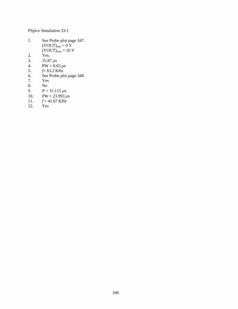
PSpice Simulation 33-1 1. See Probe plot page 347. (VOUT)min = 0 V (VOUT)max = 10 V 2. Yes. 3. 15.87 μs 4. PW = 8.63 μs 5. f= 63.2 KHz 6. See Probe plot page 348. 7. Yes 8. No 9. P = 31.115 μs 10. PW = 23.993 μs 11. f = 41.67 KHz 12. Yes
346
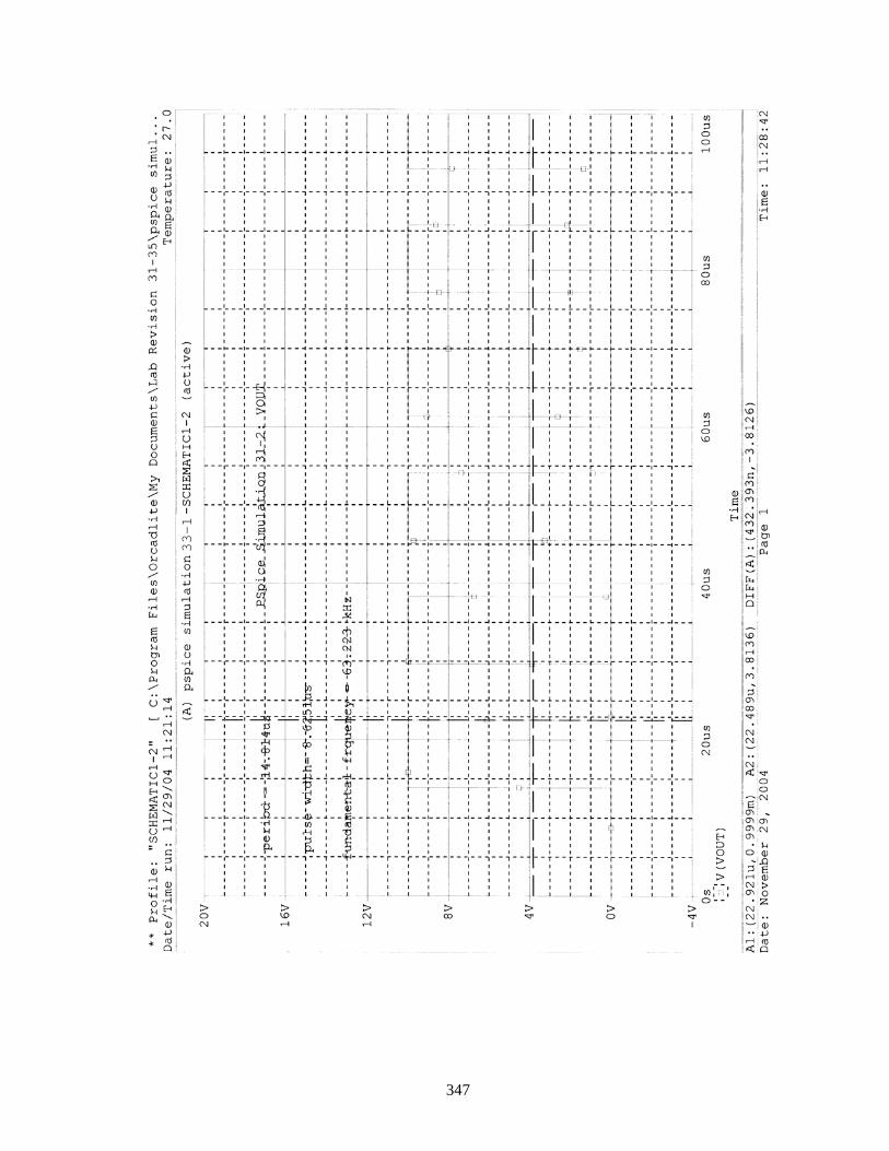
33-1
347
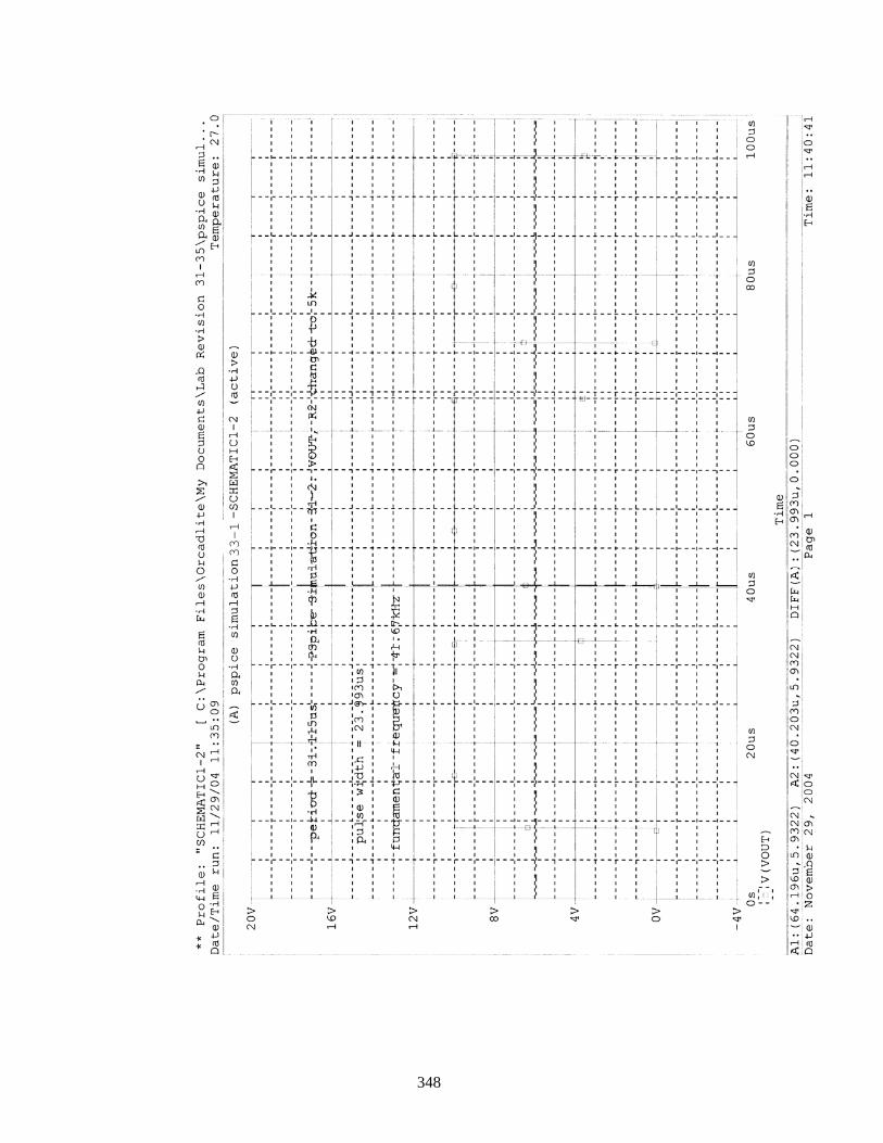
33-1
348
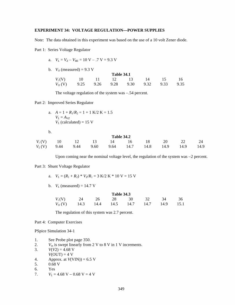
EXPERIMENT 34: VOLTAGE REGULATION—POWER SUPPLIES Note: The data obtained in this experiment was based on the use of a 10 volt Zener diode. Part 1: Series Voltage Regulator a. VL = VZ − VBE = 10 V − .7 V = 9.3 V b. VO (measured) = 9.3 V
Table 34.1 Vi (V) 10 11 12 13 14 15 16 VO (V) 9.25 9.26 9.28 9.30 9.32 9.33 9.35
The voltage regulation of the system was −.54 percent. Part 2: Improved Series Regulator a. A = 1 + R1/R2 = 1 + 1 K/2 K = 1.5 VL = AVZ VL (calculated) = 15 V b.
Table 34.2 Vi (V) 10 12 13 14 16 18 20 22 24 VL (V) 9.44 9.44 9.60 9.64 14.7 14.8 14.9 14.9 14.9
Upon coming near the nominal voltage level, the regulation of the system was −2 percent. Part 3: Shunt Voltage Regulator a. VL = (R1 + R2) * VZ/R1 = 3 K/2 K * 10 V = 15 V b. VL (measured) = 14.7 V
Table 34.3 Vi (V) 24 26 28 30 32 34 36 VO (V) 14.3 14.4 14.5 14.7 14.7 14.9 15.1
The regulation of this system was 2.7 percent. Part 4: Computer Exercises PSpice Simulation 34-1 1. See Probe plot page 350. 2. Vin is swept linearly from 2 V to 8 V in 1 V increments. 3. V(V2) = 4.68 V V(OUT) = 4 V 4. Approx. at V(VIN)) = 6.5 V 5. 0.68 V 6. Yes 7. VL = 4.68 V − 0.68 V = 4 V
349
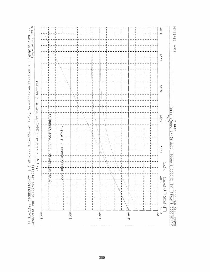
34-1
350
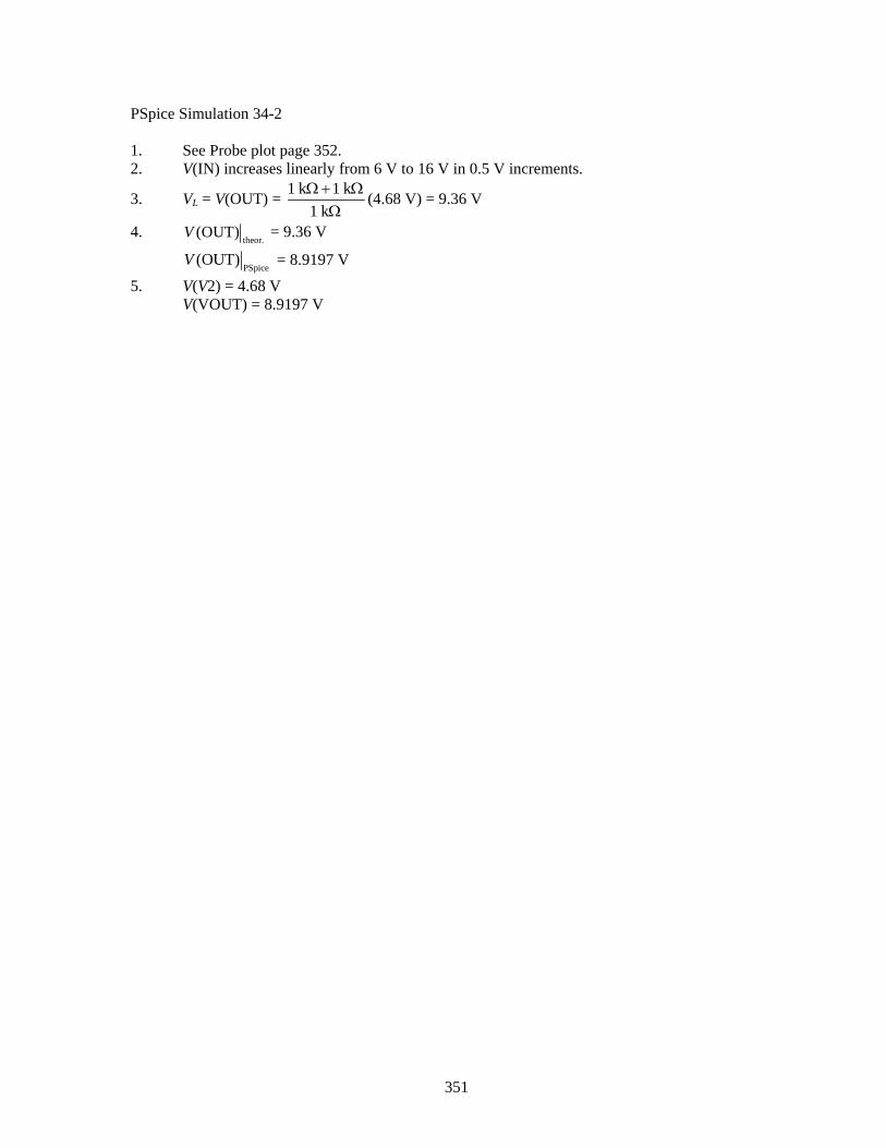
PSpice Simulation 34-2 1. See Probe plot page 352. 2. V(IN) increases linearly from 6 V to 16 V in 0.5 V increments.
3. VL = V(OUT) = 1 k 1 k1 kΩ+ Ω
Ω(4.68 V) = 9.36 V
4. theor.
(OUT)V = 9.36 V
PSpice(OUT)V = 8.9197 V
5. V(V2) = 4.68 V V(VOUT) = 8.9197 V
351
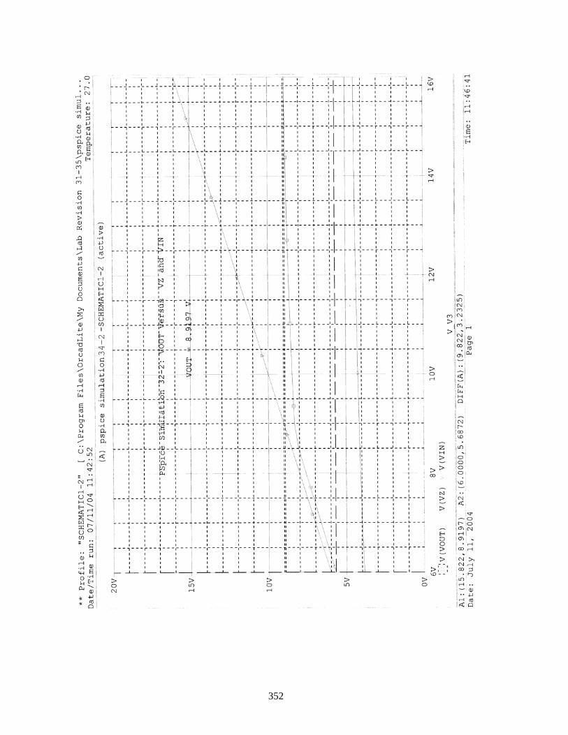
34-2
352
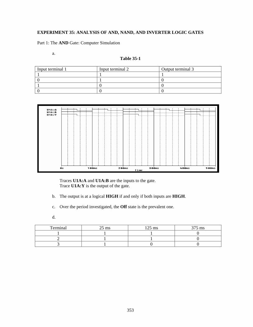
EXPERIMENT 35: ANALYSIS OF AND, NAND, AND INVERTER LOGIC GATES Part 1: The AND Gate: Computer Simulation a.
Table 35-1 Input terminal 1 Input terminal 2 Output terminal 3 1 1 1 0 1 0 1 0 0 0 0 0
Traces U1A:A and U1A:B are the inputs to the gate. Trace U1A:Y is the output of the gate.
b. The output is at a logical HIGH if and only if both inputs are HIGH. c. Over the period investigated, the Off state is the prevalent one. d.
Terminal 25 ms 125 ms 375 ms
1 1 1 0 2 1 1 0 3 1 0 0
353
Part 2. The AND Gate: Experimental Determination of Logic States
a. Ideally, the same. b. 10 Hz c. Should be the same as that for the simulation. d. The amplitude of the TTL pulses are about 5 volts, that of the Output terminal 3 is about 3.5 volts. e. The internal voltage drop of across the gate causes the difference between these voltage levels.
Part 3: Logic States versus Voltage Levels
b. Example of a calculation: assume: V(V1A:Y) = 3.5 volts, VY = 3.4 volts
3.5V 3.4V%deviation *100 2.86 percent3.5V−
= =
c. For this particular example, the calculated percent deviation falls well within the
permissible range. Part 4: Propagation delay
a. For the current case, the propagation delay at the lagging edge of the applied TTL pulse should be identical to that at the leading edge of that pulse. Thus, it should measure about 18 nanoseconds. b. Ideally, the propagation delays determined by the simulation should be identical to that determined in the laboratory. c. From Laboratory data, determine the percent deviation using the same procedure as
before.
354
Part 5: NOT-AND Logic A. Computer Simulation a.
Table 35-2
Input1(7408) Input 2(7408) Input1(7404) Output(7404) 1 1 1 0 0 1 0 1 1 0 0 1 0 0 0 1
Traces U1A: A and U1A:B are the inputs to the 7408 gate, U1A:Y its output trace. Trace U2A:Y is the output of the 7404 gate.
b. The Output of the 7404 gate will be HIGH if and only if the input to both terminals of the 7408 gate are HIGH, otherwise, the output of the 7404 gate will be LOW.
c. The most prevalent state of the Output terminal of the 7404 gate is HIGH. d. The PSpice cursor was used to determine the logic states at the requested times. The logic
states are indicated at the left margin. At t = 25 milliseconds:
A1 = 25.397m, 1 A2 = 0.000, 1 dif = 25.397m
355
At t = 125 milliseconds
A1 = 125.397m, 1 A2 = 0.000, 1 dif = 125.397m
At t = 375 milliseconds
A1 = 375.397m, 0 A2 = 0.000, 1 dif = 375.397m
B. Experimental Determination of Logic States a. They should be relatively close to each other. b. They are identical. c. The output of the 7404 gate is the negation of the output of the 7408 gate.
356
Part 6: The 7400 NAND Gate A. Computer Simulation
Table 35-3 a. Input terminal 1 Input terminal 2 Output terminal 3
1 1 0 0 1 1 1 0 1 0 0 1
b.
B. Experimental Determination of Logic States
Table 35-4
Input terminal 1 Input terminal 2 Output terminal 3
1 1 0 0 1 1 1 0 1 0 0 1
357
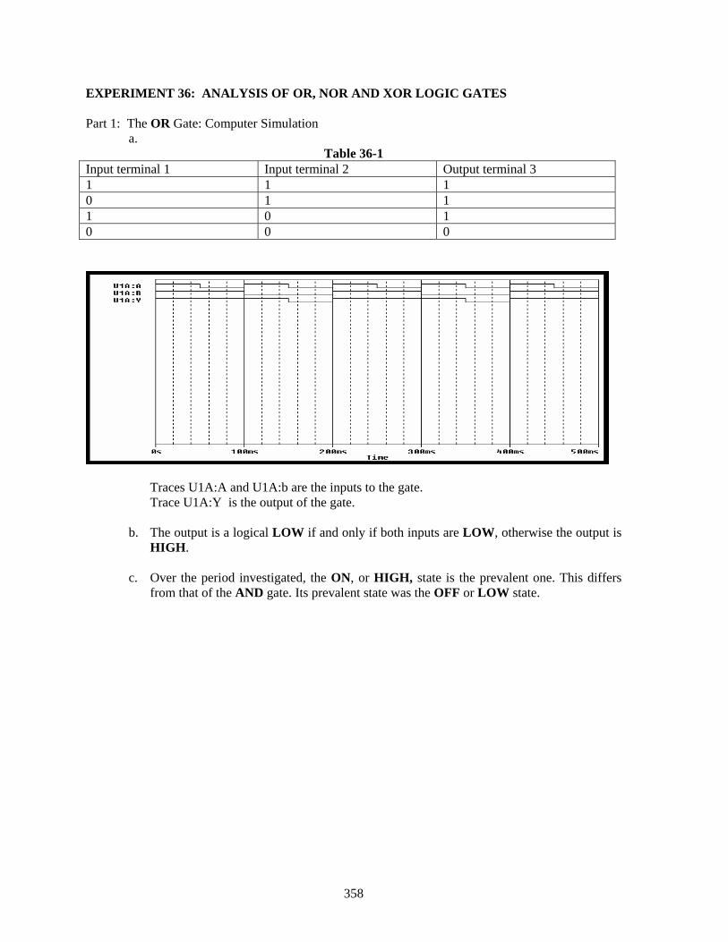
EXPERIMENT 36: ANALYSIS OF OR, NOR AND XOR LOGIC GATES Part 1: The OR Gate: Computer Simulation
a. Table 36-1
Input terminal 1 Input terminal 2 Output terminal 3 1 1 1 0 1 1 1 0 1 0 0 0
Traces U1A:A and U1A:b are the inputs to the gate. Trace U1A:Y is the output of the gate.
b. The output is a logical LOW if and only if both inputs are LOW, otherwise the output is HIGH.
c. Over the period investigated, the ON, or HIGH, state is the prevalent one. This differs
from that of the AND gate. Its prevalent state was the OFF or LOW state.
358
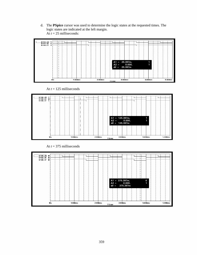
d. The PSpice cursor was used to determine the logic states at the requested times. The logic states are indicated at the left margin.
At t = 25 milliseconds:
A1 = 25.397m, 1 A2 = 0.000, 1 dif = 25.397m
At t = 125 milliseconds
A1 = 125.397m, 1 A2 = 0.000, 1 dif = 125.397m
At t = 375 milliseconds
A1 = 375.397m, 0 A2 = 0.000, 1 dif = 375.397m
359
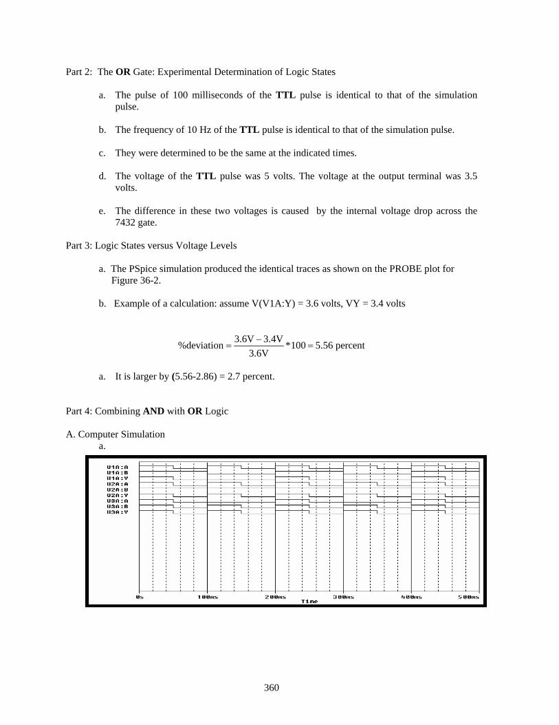
Part 2: The OR Gate: Experimental Determination of Logic States
a. The pulse of 100 milliseconds of the TTL pulse is identical to that of the simulation pulse.
b. The frequency of 10 Hz of the TTL pulse is identical to that of the simulation pulse. c. They were determined to be the same at the indicated times. d. The voltage of the TTL pulse was 5 volts. The voltage at the output terminal was 3.5
volts. e. The difference in these two voltages is caused by the internal voltage drop across the
7432 gate. Part 3: Logic States versus Voltage Levels
a. The PSpice simulation produced the identical traces as shown on the PROBE plot for Figure 36-2. b. Example of a calculation: assume V(V1A:Y) = 3.6 volts, VY = 3.4 volts
3.6V 3.4V%deviation *100 5.56 percent3.6V−
= =
a. It is larger by (5.56-2.86) = 2.7 percent.
Part 4: Combining AND with OR Logic A. Computer Simulation a.
360
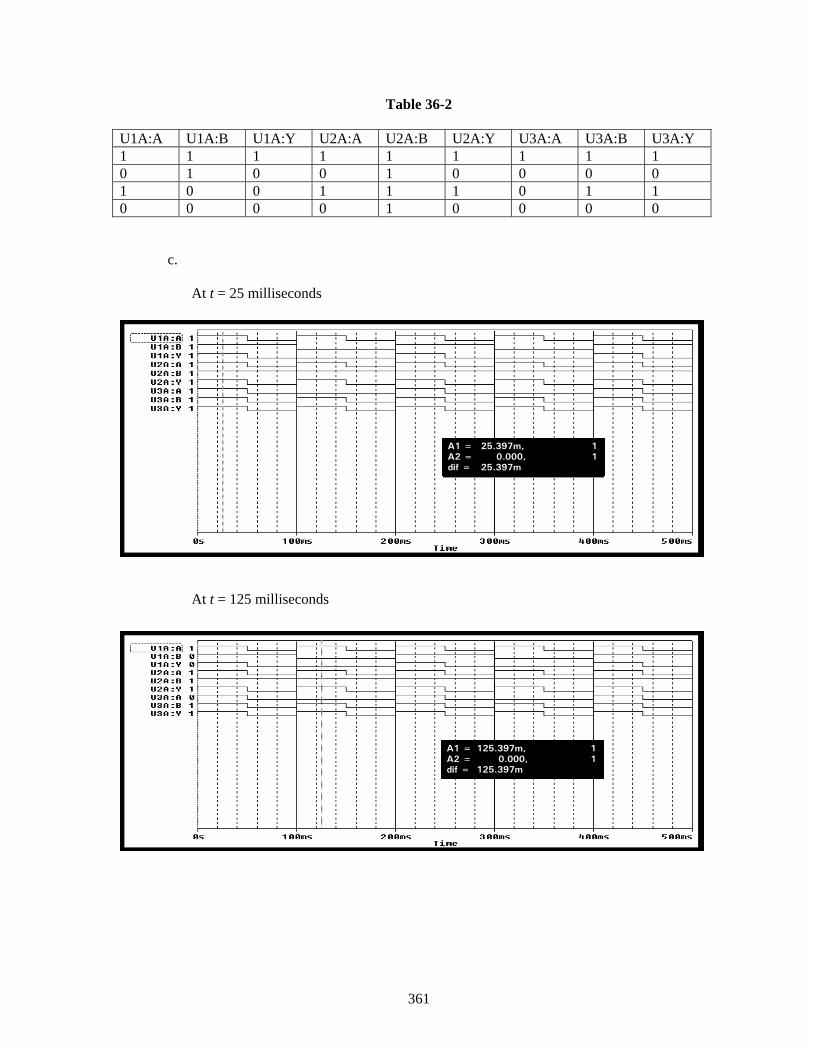
Table 36-2
U1A:A U1A:B U1A:Y U2A:A U2A:B U2A:Y U3A:A U3A:B U3A:Y 1 1 1 1 1 1 1 1 1 0 1 0 0 1 0 0 0 0 1 0 0 1 1 1 0 1 1 0 0 0 0 1 0 0 0 0
c. At t = 25 milliseconds
A1 = 25.397m, 1 A2 = 0.000, 1 dif = 25.397m
At t = 125 milliseconds
A1 = 125.397m, 1 A2 = 0.000, 1 dif = 125.397m
361
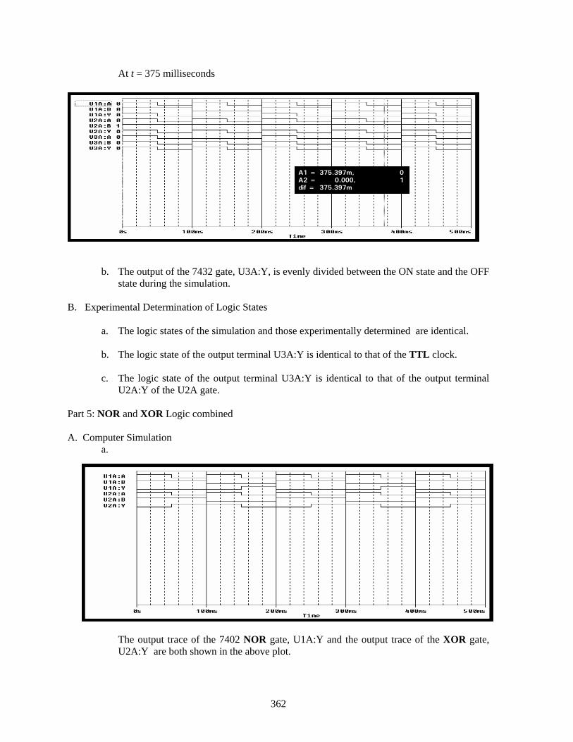
At t = 375 milliseconds
A1 = 375.397m, 0 A2 = 0.000, 1 dif = 375.397m
b. The output of the 7432 gate, U3A:Y, is evenly divided between the ON state and the OFF state during the simulation.
B. Experimental Determination of Logic States
a. The logic states of the simulation and those experimentally determined are identical. b. The logic state of the output terminal U3A:Y is identical to that of the TTL clock. c. The logic state of the output terminal U3A:Y is identical to that of the output terminal
U2A:Y of the U2A gate. Part 5: NOR and XOR Logic combined A. Computer Simulation a.
The output trace of the 7402 NOR gate, U1A:Y and the output trace of the XOR gate,
U2A:Y are both shown in the above plot.
362
b. Table 36-3
U1A:A U1A:B U1A:Y U2A:A U2A:B U2A:Y 1 1 0 1 1 0 0 1 0 0 1 1 1 0 0 1 0 1 0 0 1 0 0 0
c. The output of the 7402 gate, U1A:Y is HIGH if and only if both inputs are LOW, otherwise the output is LOW.
d. This is a logical inversion of the OR gate. c. The output of the 7486 gate is HIGH if and only if the two inputs U2A:A and U2A:B
are at opposite logic levels. f. The logic state of the OR gate is HIGH if both inputs are at opposite logic levels and if
both inputs are HIGH. B. Experimental Determination of Logic States
a. The experimental data is identical to that obtained from the simulation. b. Refer to the data in Table 36-3. c. Refer to the data in Table 36-3. d. Refer to the data in Table 36-3. e. The output of the 7486 XOR gate is HIGH if and only if its input terminals have
opposite logic levels, otherwise, its output is at a LOW. f. For an OR gate, its output is HIGH if both, or at least one input terminal, is HIGH. Its output will be LOW if both inputs are LOW. For an XOR gate, its output is HIGH if
and only if both input terminals are at opposite logic levels, otherwise, the output will be LOW.
g. The output of an XOR gate will be HIGH when both input terminals are at opposite
logic levels. Otherwise, its output is at a logical LOW.
363
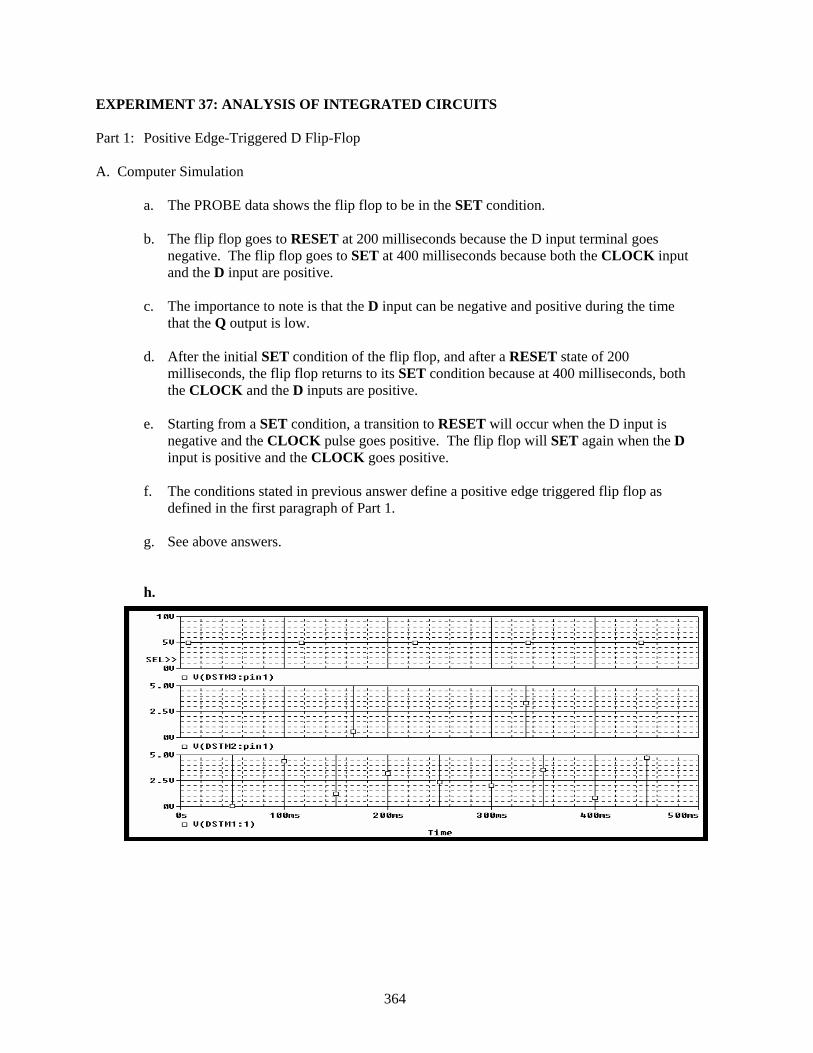
EXPERIMENT 37: ANALYSIS OF INTEGRATED CIRCUITS Part 1: Positive Edge-Triggered D Flip-Flop A. Computer Simulation
a. The PROBE data shows the flip flop to be in the SET condition. b. The flip flop goes to RESET at 200 milliseconds because the D input terminal goes
negative. The flip flop goes to SET at 400 milliseconds because both the CLOCK input and the D input are positive.
c. The importance to note is that the D input can be negative and positive during the time
that the Q output is low. d. After the initial SET condition of the flip flop, and after a RESET state of 200
milliseconds, the flip flop returns to its SET condition because at 400 milliseconds, both the CLOCK and the D inputs are positive.
e. Starting from a SET condition, a transition to RESET will occur when the D input is
negative and the CLOCK pulse goes positive. The flip flop will SET again when the D input is positive and the CLOCK goes positive.
f. The conditions stated in previous answer define a positive edge triggered flip flop as
defined in the first paragraph of Part 1. g. See above answers. h.
364
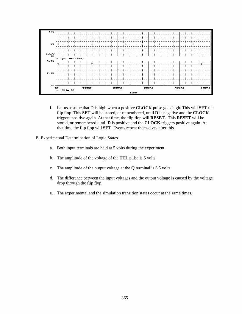
i. Let us assume that D is high when a positive CLOCK pulse goes high. This will SET the flip flop. This SET will be stored, or remembered, until D is negative and the CLOCK triggers positive again. At that time, the flip flop will RESET. This RESET will be stored, or remembered, until D is positive and the CLOCK triggers positive again. At that time the flip flop will SET. Events repeat themselves after this.
B. Experimental Determination of Logic States
a. Both input terminals are held at 5 volts during the experiment. b. The amplitude of the voltage of the TTL pulse is 5 volts. c. The amplitude of the output voltage at the Q terminal is 3.5 volts. d. The difference between the input voltages and the output voltage is caused by the voltage
drop through the flip flop. e. The experimental and the simulation transition states occur at the same times.
365
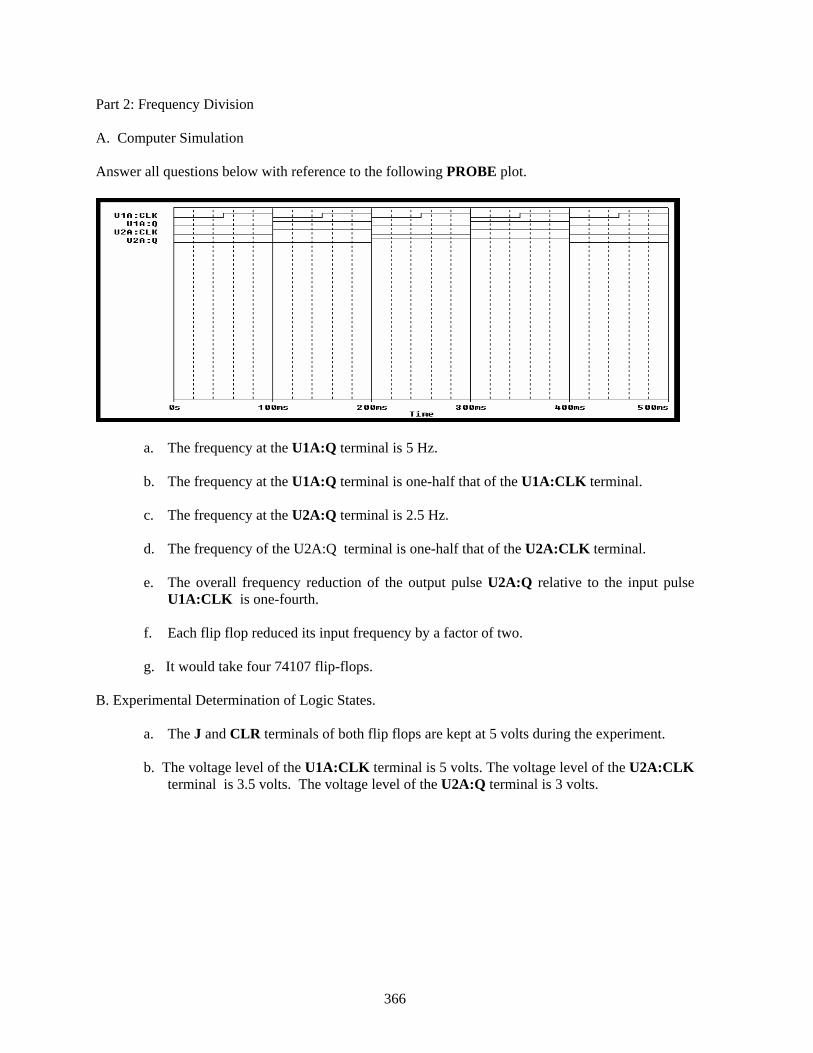
Part 2: Frequency Division A. Computer Simulation Answer all questions below with reference to the following PROBE plot.
a. The frequency at the U1A:Q terminal is 5 Hz. b. The frequency at the U1A:Q terminal is one-half that of the U1A:CLK terminal. c. The frequency at the U2A:Q terminal is 2.5 Hz. d. The frequency of the U2A:Q terminal is one-half that of the U2A:CLK terminal. e. The overall frequency reduction of the output pulse U2A:Q relative to the input pulse
U1A:CLK is one-fourth. f. Each flip flop reduced its input frequency by a factor of two. g. It would take four 74107 flip-flops.
B. Experimental Determination of Logic States. a. The J and CLR terminals of both flip flops are kept at 5 volts during the experiment. b. The voltage level of the U1A:CLK terminal is 5 volts. The voltage level of the U2A:CLK
terminal is 3.5 volts. The voltage level of the U2A:Q terminal is 3 volts.
366
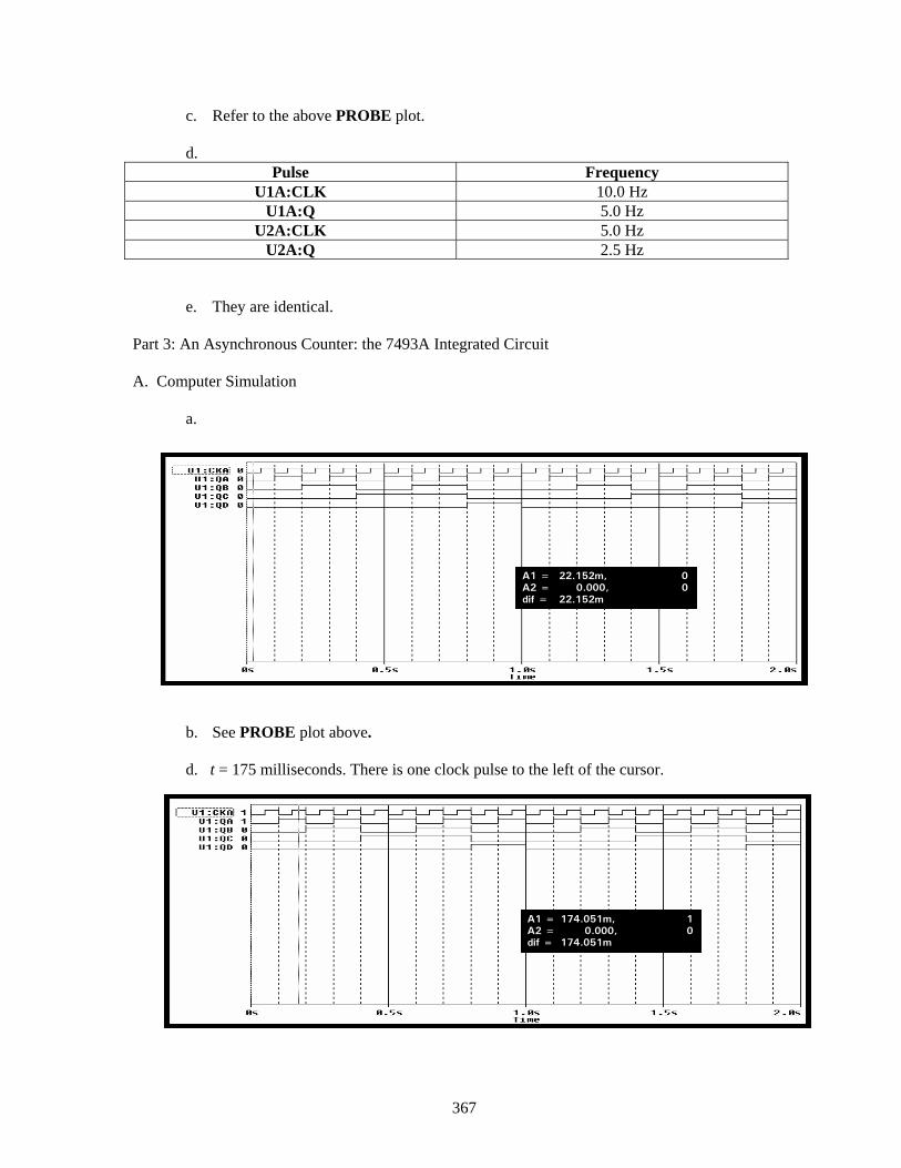
c. Refer to the above PROBE plot. d.
Pulse Frequency U1A:CLK 10.0 Hz
U1A:Q 5.0 Hz U2A:CLK 5.0 Hz
U2A:Q 2.5 Hz
e. They are identical. Part 3: An Asynchronous Counter: the 7493A Integrated Circuit A. Computer Simulation
a.
A1 = 22.152m, 0 A2 = 0.000, 0 dif = 22.152m
b. See PROBE plot above. d. t = 175 milliseconds. There is one clock pulse to the left of the cursor.
A1 = 174.051m, 1 A2 = 0.000, 0 dif = 174.051m
367
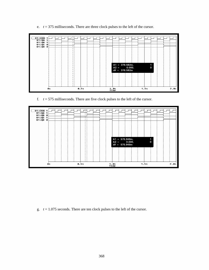
e. t = 375 milliseconds. There are three clock pulses to the left of the cursor.
f. t = 575 milliseconds. There are five clock pulses to the left of the cursor.
g. t = 1.075 seconds. There are ten clock pulses to the left of the cursor.
A1 = 376.582m, 1 A2 = 0.000, 0 dif = 376.582m
A1 = 575.949m, 1 A2 = 0.000, 0 dif = 575.949m
368
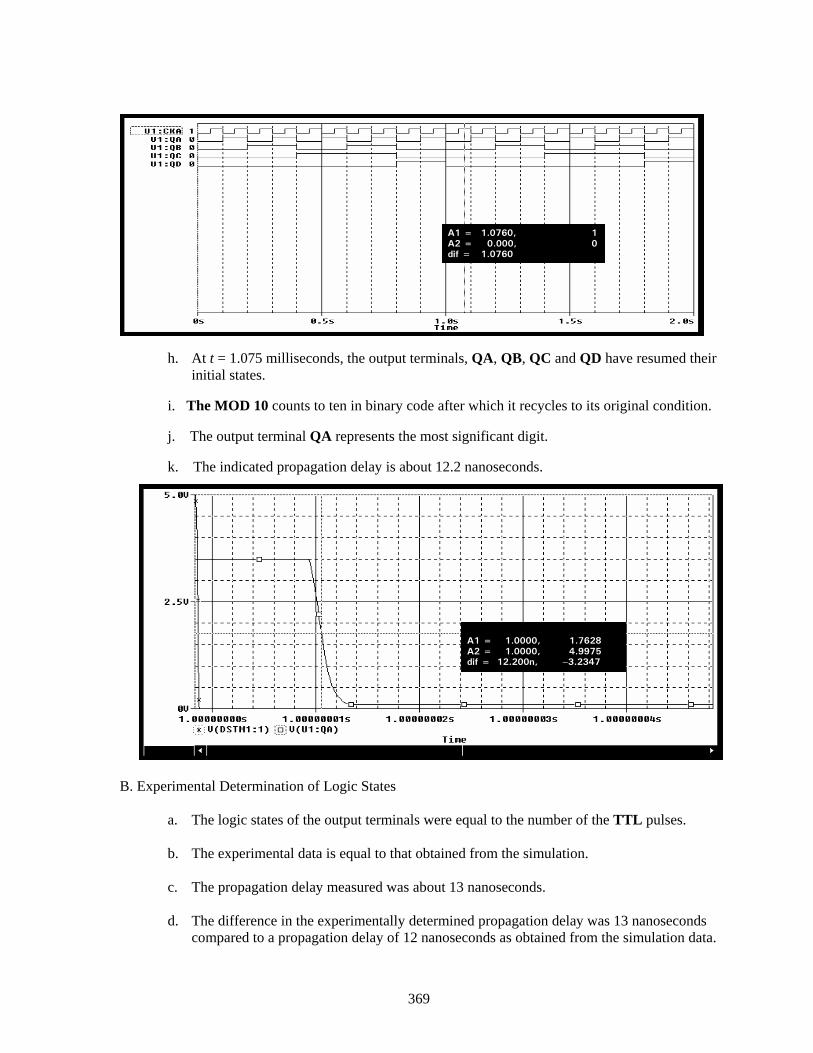
le riginal condition. j. The output terminal QA represents the most significant digit. k. The indicated propagation delay is about 12.2 nanoseconds.
B. Experimental Determination of Logic States
a. The logic states of the output terminals were equal to the number of the TTL pulses. b. The experimental data is equal to that obtained from the simulation. c. The propagation delay measured was about 13 nanoseconds. d. The difference in the experimentally determined propagation delay was 13 nanoseconds
compared to a propagation delay of 12 nanoseconds as obtained from the simulation data.
h. At t = 1.075 milliseconds, the output terminals, QA, QB, QC and QD have resumed their initial states.
i. The MOD 10 counts to ten in binary code after whic it recyc s to its oh
A1 = 1.0760, 1 A2 = 0.000, 0 dif = 1.0760
A1 = 1.0000, A2 = 1.0000,
1.7628 4.9975
dif = 12.200n, −3.2347
369