Embed Size (px)
Citation preview
Chapter 12
IMPLEMENTATION OF COMBINATIONAL LOGIC BY
STANDARD ICs and PROGRAMMABLE ROM
MEMORIES
Ch12L2-"Digital Principles and Design", Raj Kamal, Pearson Education, 2006 2
Lesson 2
Read Only Memory (ROM)
Ch12L2-"Digital Principles and Design", Raj Kamal, Pearson Education, 2006 3
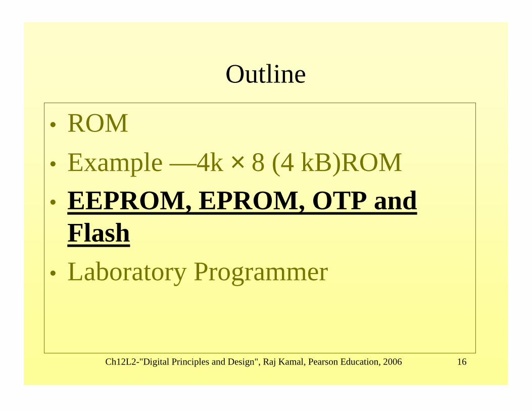
Outline
• ROM• Example —4k × 8 (4 kB)ROM • EEPROM, EPROM, OTP and Flash• Laboratory Programmer
Ch12L2-"Digital Principles and Design", Raj Kamal, Pearson Education, 2006 4
ROM• Read only memory• Read means output data-bits corresponding to the
address bits set at the input. The bits are used by some processor or device or circuit for further operations.
• Data bits of different addresses store at ROM and all bits remain stored in the memory even after a power interruption or power switch OFF
• ROM is randomly accessed. An equal time interval is taken for a read of data-bits from each address. Address bits can be set randomly by an external circuit.
Ch12L2-"Digital Principles and Design", Raj Kamal, Pearson Education, 2006 5
ROM• ROM is a previously programmed
‘Decoder-diode links’ array based logic device, programmed using appropriate masks at the manufacturing stage or by laboratory programming device
• ROM has an address decoder (n to 2n
decoder) within it• Each output line of decoder has 8
connections through a fusible diode. A diode n-end connects to a data bit output.
Ch12L2-"Digital Principles and Design", Raj Kamal, Pearson Education, 2006 6
ROM• There are 8 data output lines D0-D7• Each output line Y of decoder has 8 connections
through the fusible link to diode. The diode n-ends connect to the data bit outputs and p-ends to Y . The n-ends also connect to ground line. Y is in tristate and only that Y is 1, which corresponds to address at input pins.
• A data bit is 1 when the corresponding diode link is not fused during masking, and 0 when fused. All diodes links are programmed by masking process such that only programmed diode links are fused and give 0s.
Ch12L2-"Digital Principles and Design", Raj Kamal, Pearson Education, 2006 7
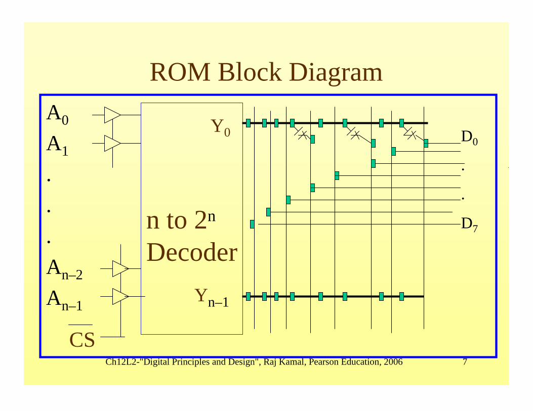
ROM Block DiagramA0
A1
.
.
.An–2
An–1
CS
n to 2n
Decoder
Y0
Yn–1
D0
.
.
D7
Ch12L2-"Digital Principles and Design", Raj Kamal, Pearson Education, 2006 8
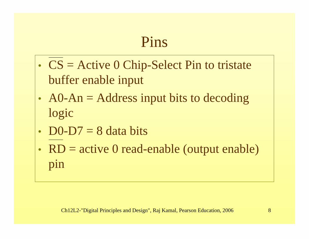
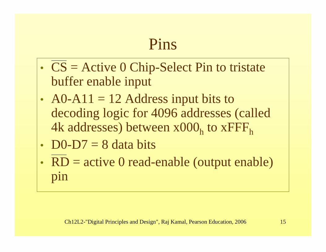
Pins• CS = Active 0 Chip-Select Pin to tristate
buffer enable input• A0-An = Address input bits to decoding
logic• D0-D7 = 8 data bits• RD = active 0 read-enable (output enable)
pin
Ch12L2-"Digital Principles and Design", Raj Kamal, Pearson Education, 2006 9
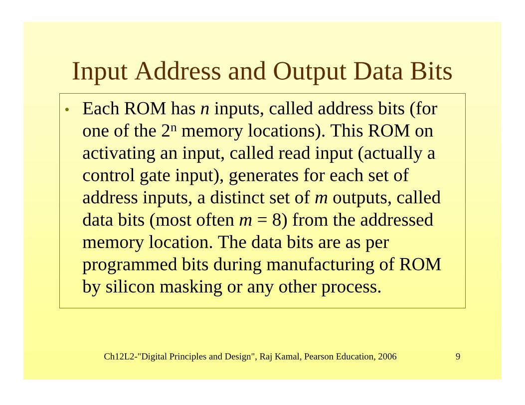
Input Address and Output Data Bits• Each ROM has n inputs, called address bits (for
one of the 2n memory locations). This ROM on activating an input, called read input (actually a control gate input), generates for each set of address inputs, a distinct set of m outputs, called data bits (most often m = 8) from the addressed memory location. The data bits are as per programmed bits during manufacturing of ROM by silicon masking or any other process.
Ch12L2-"Digital Principles and Design", Raj Kamal, Pearson Education, 2006 10
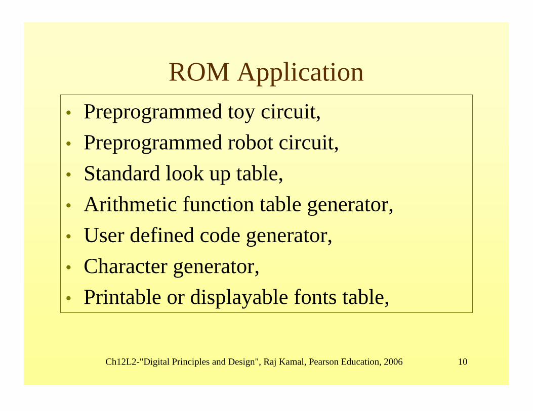
ROM Application• Preprogrammed toy circuit, • Preprogrammed robot circuit, • Standard look up table, • Arithmetic function table generator, • User defined code generator, • Character generator, • Printable or displayable fonts table,
Ch12L2-"Digital Principles and Design", Raj Kamal, Pearson Education, 2006 11
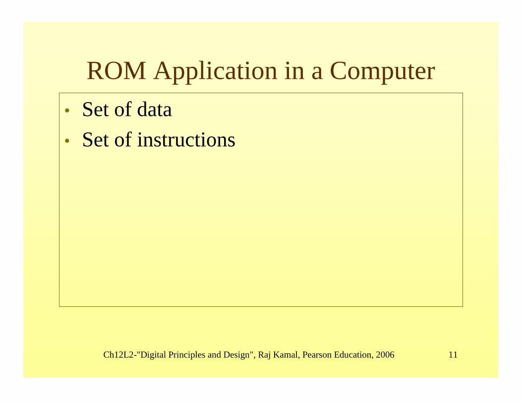
ROM Application in a Computer• Set of data • Set of instructions
Ch12L2-"Digital Principles and Design", Raj Kamal, Pearson Education, 2006 12
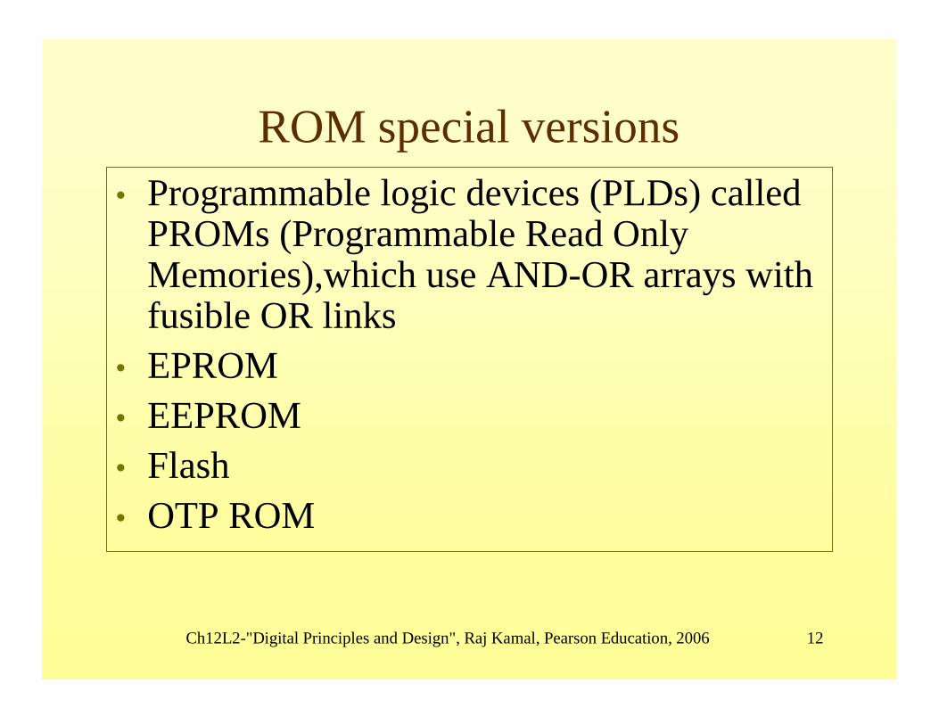
ROM special versions• Programmable logic devices (PLDs) called
PROMs (Programmable Read Only Memories),which use AND-OR arrays with fusible OR links
• EPROM • EEPROM • Flash• OTP ROM
Ch12L2-"Digital Principles and Design", Raj Kamal, Pearson Education, 2006 13
Outline
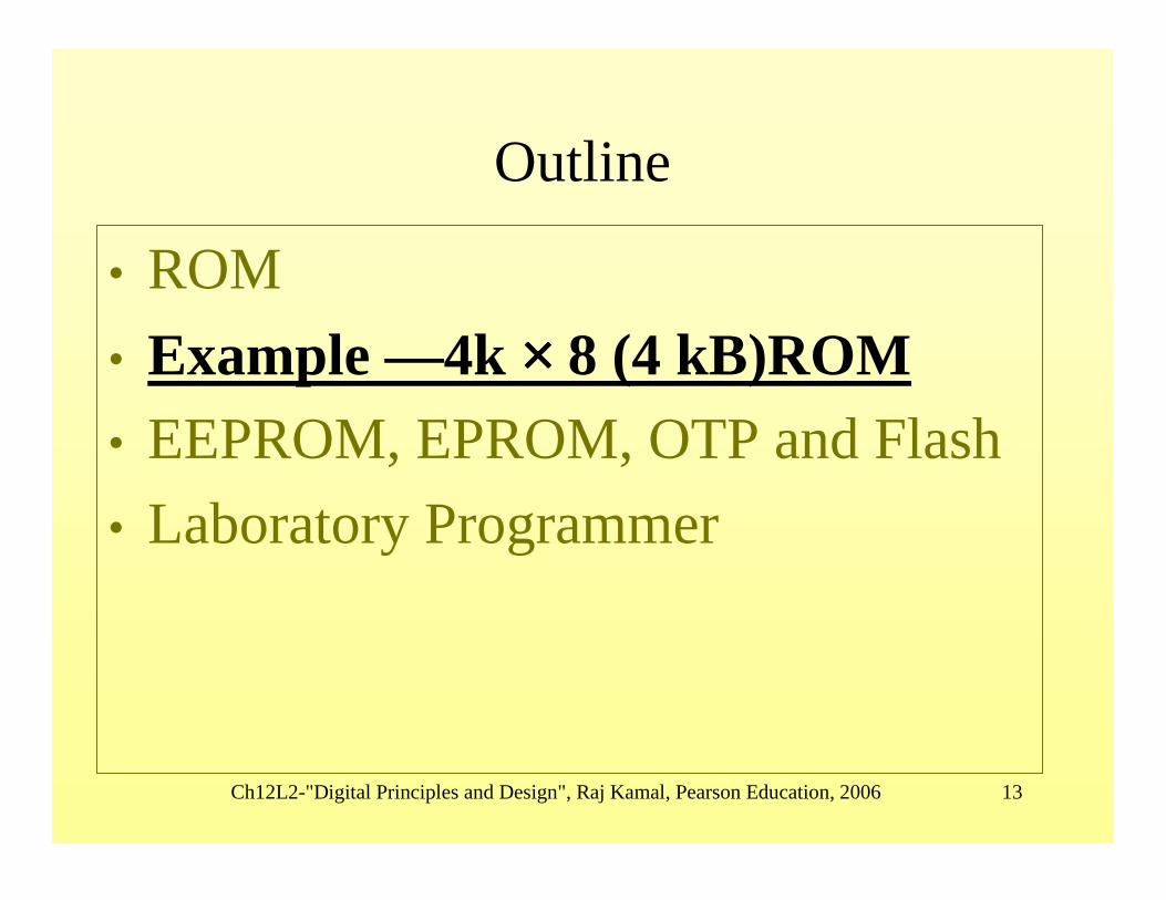
• ROM• Example —4k ×××× 8 (4 kB)ROM • EEPROM, EPROM, OTP and Flash• Laboratory Programmer
Ch12L2-"Digital Principles and Design", Raj Kamal, Pearson Education, 2006 14
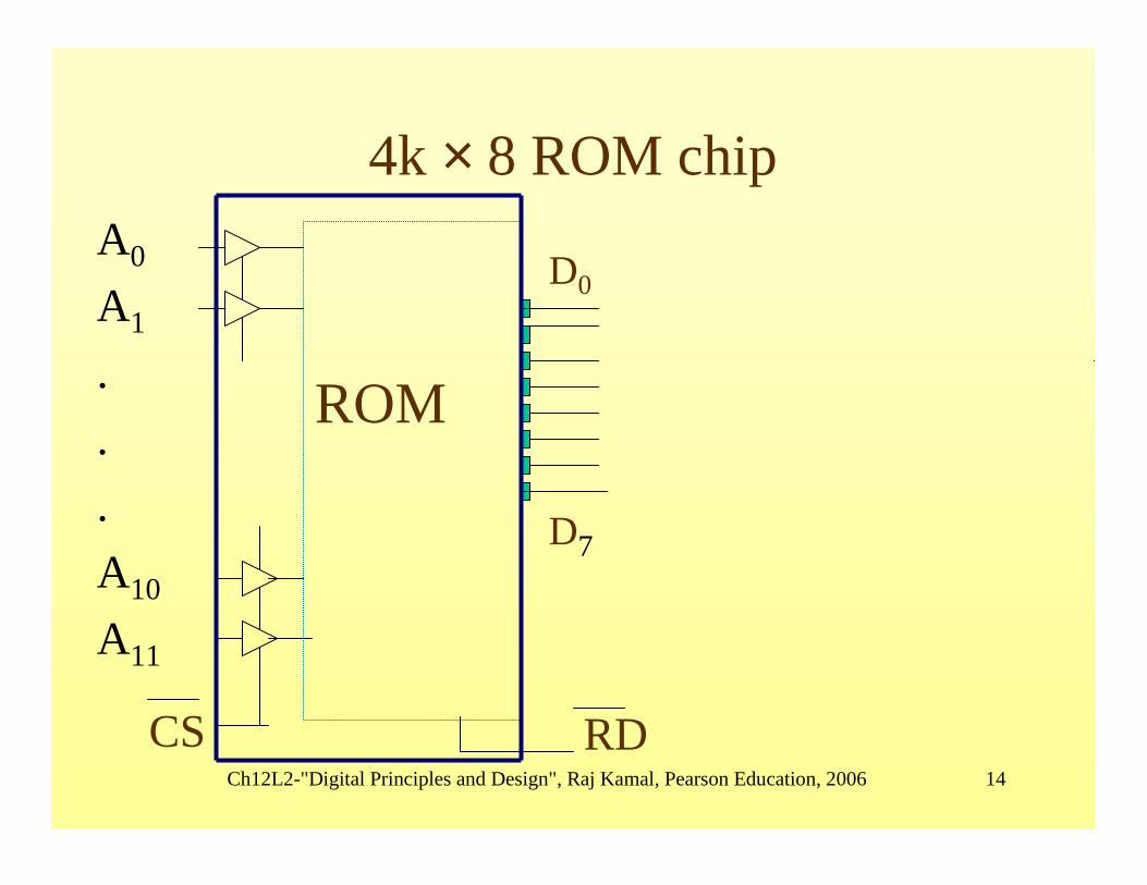
4k × 8 ROM chipA0
A1
.
.
.A10
A11
CS
ROM
D0
D7
RD
Ch12L2-"Digital Principles and Design", Raj Kamal, Pearson Education, 2006 15
Pins• CS = Active 0 Chip-Select Pin to tristate
buffer enable input• A0-A11 = 12 Address input bits to
decoding logic for 4096 addresses (called 4k addresses) between x000h to xFFFh
• D0-D7 = 8 data bits• RD = active 0 read-enable (output enable)
pin
Ch12L2-"Digital Principles and Design", Raj Kamal, Pearson Education, 2006 16
Outline
• ROM• Example —4k × 8 (4 kB)ROM • EEPROM, EPROM, OTP and
Flash• Laboratory Programmer
Ch12L2-"Digital Principles and Design", Raj Kamal, Pearson Education, 2006 17
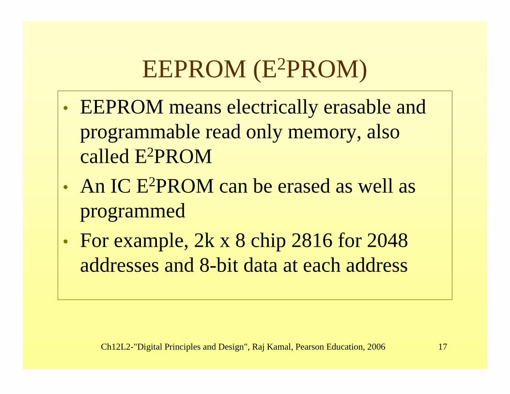
EEPROM (E2PROM)• EEPROM means electrically erasable and
programmable read only memory, also called E2PROM
• An IC E2PROM can be erased as well as programmed
• For example, 2k x 8 chip 2816 for 2048 addresses and 8-bit data at each address
Ch12L2-"Digital Principles and Design", Raj Kamal, Pearson Education, 2006 18
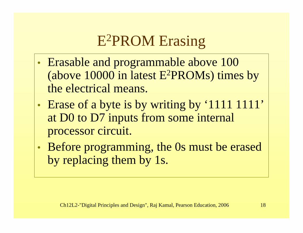
E2PROM Erasing• Erasable and programmable above 100
(above 10000 in latest E2PROMs) times by the electrical means.
• Erase of a byte is by writing by ‘1111 1111’at D0 to D7 inputs from some internal processor circuit.
• Before programming, the 0s must be erased by replacing them by 1s.
Ch12L2-"Digital Principles and Design", Raj Kamal, Pearson Education, 2006 19
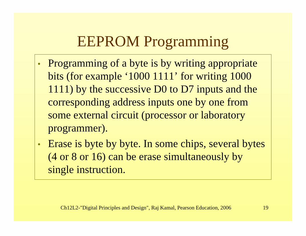
EEPROM Programming• Programming of a byte is by writing appropriate
bits (for example ‘1000 1111’ for writing 1000 1111) by the successive D0 to D7 inputs and the corresponding address inputs one by one from some external circuit (processor or laboratory programmer).
• Erase is byte by byte. In some chips, several bytes (4 or 8 or 16) can be erase simultaneously by single instruction.
Ch12L2-"Digital Principles and Design", Raj Kamal, Pearson Education, 2006 20
EEPROM• A byte is set at D0-D7 lines for writing FFh on
application of a programming pulse or instruction. FFh at an address means, the data bits at that address are in erased state.
• After erasing, a byte as per program can be written at an address on application of a programming pulse or instruction. [D0-D7 lines are set for writing any set of data bits for the address.]
Ch12L2-"Digital Principles and Design", Raj Kamal, Pearson Education, 2006 21
Flash• Flash means an EEPROM in which erase of whole
sector(s) is done in very short interval. A sector may be of 4k or 16k.
• An IC flash can be erased by an instruction All addresses of a sector or a set of sectors get erased concurrently.
• For example, 2M × 8 flash chip for 2 × 220
addresses and 8-bit data at each address and a sector of 216 bytes can erase by single instruction
Ch12L2-"Digital Principles and Design", Raj Kamal, Pearson Education, 2006 22
Flash Erasing• Erase of a byte is by writing by ‘1111 1111’
at D0 to D7 inputs • Before programming a flash for the 0s, an
instruction must erase by replacing them by 1s.
• Flash can be erased and rewritten over 10000 times.
Ch12L2-"Digital Principles and Design", Raj Kamal, Pearson Education, 2006 23
Flash Programming• Programming of a byte is by writing
appropriate bits (for example ‘1000 1111’for writing 1000 1111) by the successive D0 to D7 inputs and the corresponding address inputs one by one by a processor internal instruction or from some external circuit (called laboratory programmer).
Ch12L2-"Digital Principles and Design", Raj Kamal, Pearson Education, 2006 24
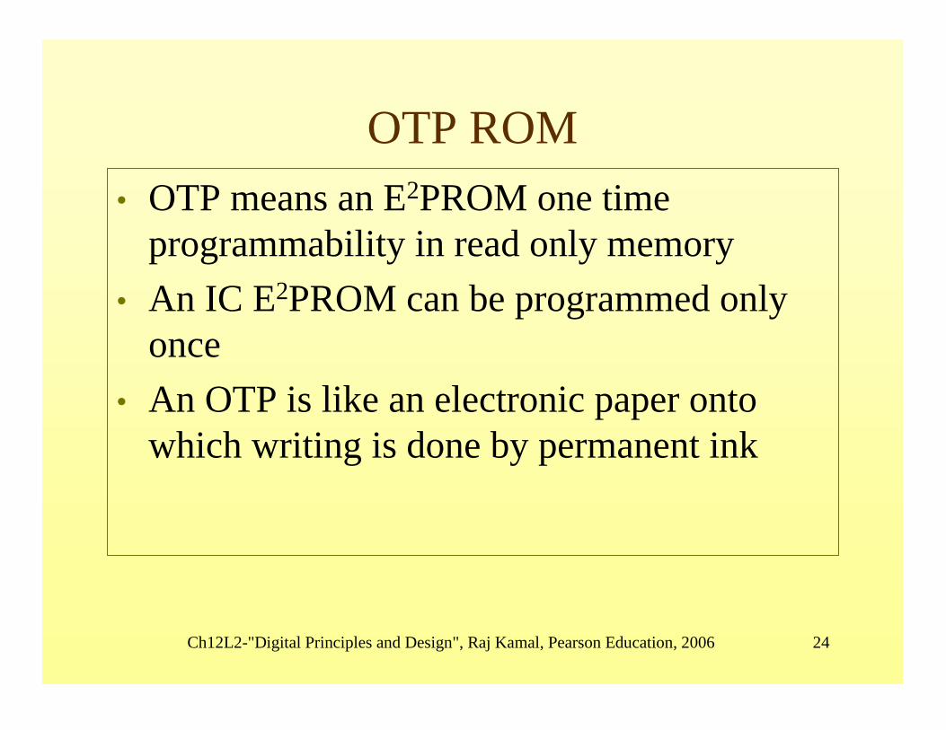
OTP ROM• OTP means an E2PROM one time
programmability in read only memory• An IC E2PROM can be programmed only
once • An OTP is like an electronic paper onto
which writing is done by permanent ink
Ch12L2-"Digital Principles and Design", Raj Kamal, Pearson Education, 2006 25
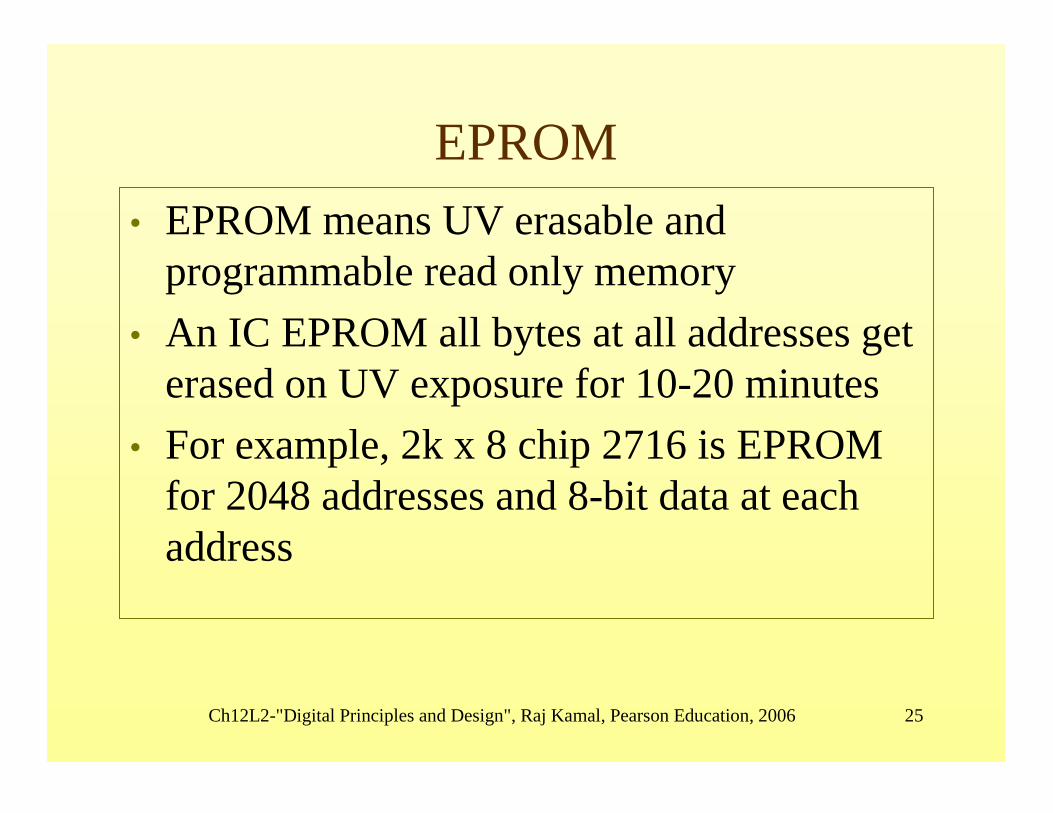
EPROM• EPROM means UV erasable and
programmable read only memory• An IC EPROM all bytes at all addresses get
erased on UV exposure for 10-20 minutes• For example, 2k x 8 chip 2716 is EPROM
for 2048 addresses and 8-bit data at each address
Ch12L2-"Digital Principles and Design", Raj Kamal, Pearson Education, 2006 26
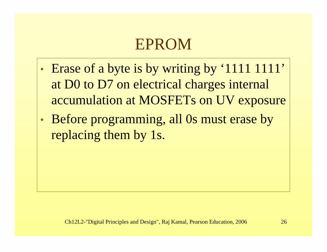
EPROM• Erase of a byte is by writing by ‘1111 1111’
at D0 to D7 on electrical charges internal accumulation at MOSFETs on UV exposure
• Before programming, all 0s must erase by replacing them by 1s.
Ch12L2-"Digital Principles and Design", Raj Kamal, Pearson Education, 2006 27
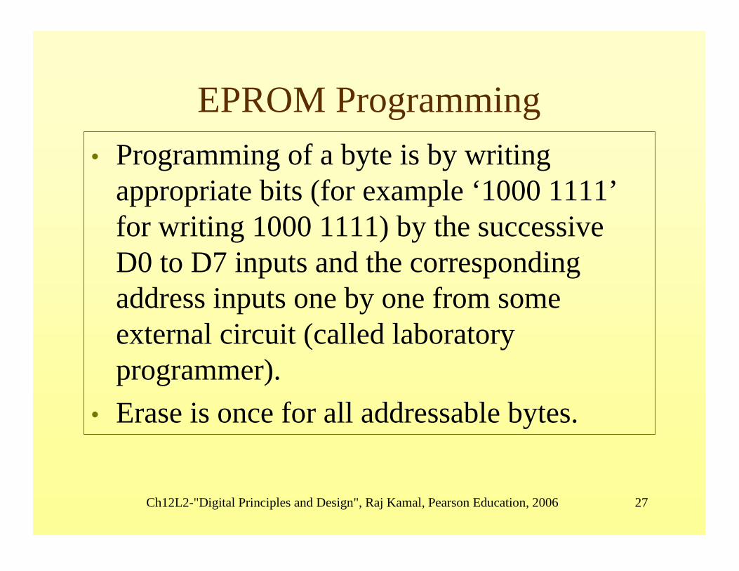
EPROM Programming• Programming of a byte is by writing
appropriate bits (for example ‘1000 1111’for writing 1000 1111) by the successive D0 to D7 inputs and the corresponding address inputs one by one from some external circuit (called laboratory programmer).
• Erase is once for all addressable bytes.
Ch12L2-"Digital Principles and Design", Raj Kamal, Pearson Education, 2006 28
EPROM• In erased EPROM, a byte as per program
can be written at an address on application of a programming pulse by laboratory programmer [D0-D7 lines are set for writing any set of data bits after setting the address bits.
Ch12L2-"Digital Principles and Design", Raj Kamal, Pearson Education, 2006 29
Outline
• ROM• Example —4k × 8 (4 kB)ROM • EEPROM, EPROM, OTP and Flash• Laboratory Programmer
Ch12L2-"Digital Principles and Design", Raj Kamal, Pearson Education, 2006 30
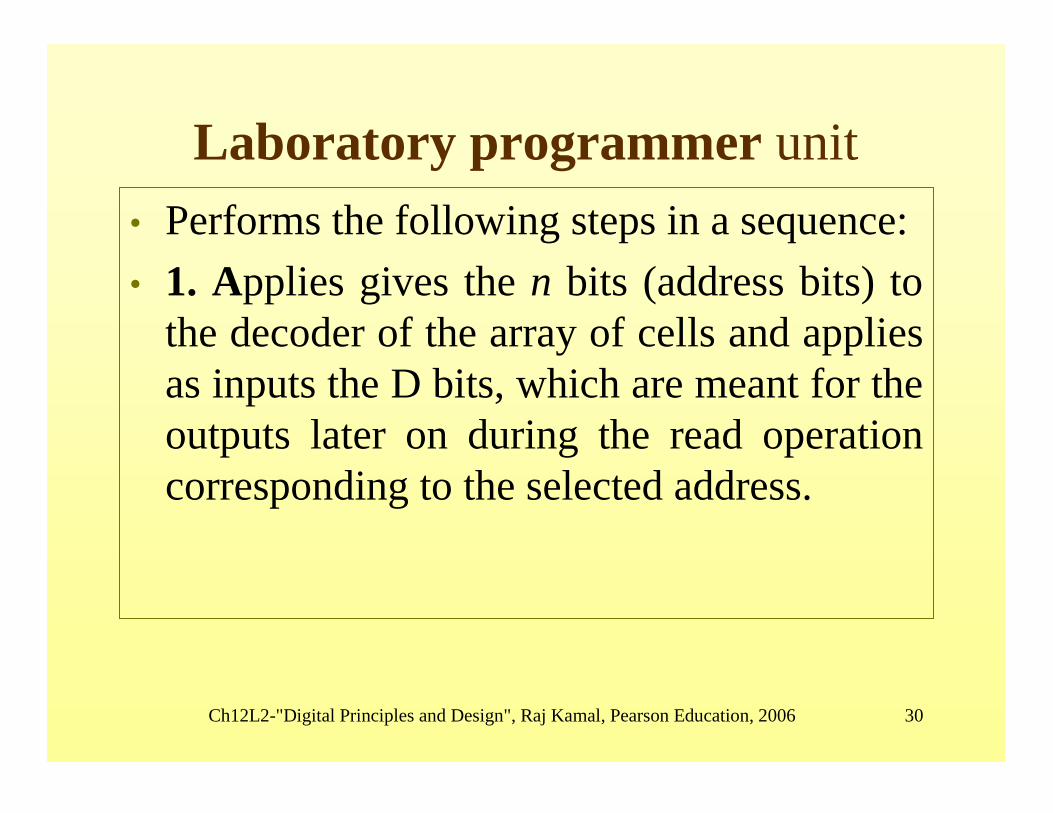
Laboratory programmer unit• Performs the following steps in a sequence:• 1. Applies gives the n bits (address bits) to
the decoder of the array of cells and applies as inputs the D bits, which are meant for the outputs later on during the read operation corresponding to the selected address.
Ch12L2-"Digital Principles and Design", Raj Kamal, Pearson Education, 2006 31
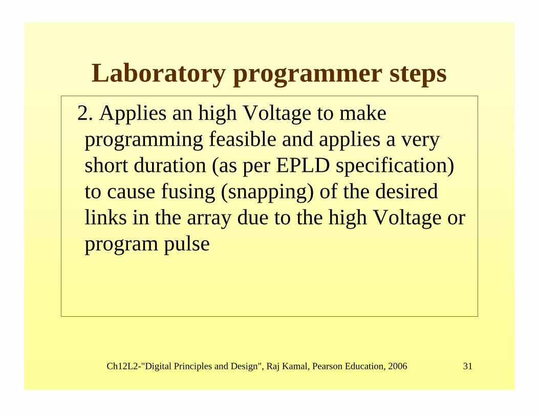
Laboratory programmer steps2. Applies an high Voltage to make programming feasible and applies a very short duration (as per EPLD specification) to cause fusing (snapping) of the desired links in the array due to the high Voltage or program pulse
Ch12L2-"Digital Principles and Design", Raj Kamal, Pearson Education, 2006 32
Laboratory programmer steps• 3. Repeat from the step 1 by applying the
next higher address than the previous one, • 4. Repetition is till all addressed are
programmed. 5.Verify the programmed bits
Ch12L2-"Digital Principles and Design", Raj Kamal, Pearson Education, 2006 33
Summary
Ch12L2-"Digital Principles and Design", Raj Kamal, Pearson Education, 2006 34
• ROM is a read only memory to store data bytes at the number of addresses
• ROM is preprogrammed at masking process
• ROM versions — Masked ROM, EPROM, EEPROM, Flash, OTP and PROM
• Laboratory programmer
Ch12L2-"Digital Principles and Design", Raj Kamal, Pearson Education, 2006 35
• ROM has 2n address in case of n input line • At each address, stores FFh after erasing • At each address, stores bytes according a
program• ROM has applications in Computer and in
large number of devices
Ch12L2-"Digital Principles and Design", Raj Kamal, Pearson Education, 2006 36
End of Lesson 2
Read Only Memory (ROM)

Ch12L2-"Digital Principles and Design", Raj Kamal, Pearson Education, 2006 37
THANK YOU