Embed Size (px)
DESCRIPTION
ECE 448 Lecture 3. Combinational-Circuit Building Blocks Data Flow Modeling of Combinational Logic. R e quired reading. P. Chu, FPGA Prototyping by VHDL Examples Chapter 3, RT-level combinational circuit. S. Brown and Z. Vranesic , Fundamentals of Digital Logic with VHDL Design - PowerPoint PPT Presentation
Citation preview

George Mason UniversityECE 448 – FPGA and ASIC Design with VHDL
Combinational-Circuit Building Blocks
Data Flow Modeling of Combinational Logic
ECE 448Lecture 3

2ECE 448 – FPGA and ASIC Design with VHDL
Required reading
• S. Brown and Z. Vranesic, Fundamentals of Digital Logic with VHDL Design
Chapter 6, Combinational-Circuit Building Blocks
Chapter 5.5, Design of Arithmetic Circuits Using
CAD Tools
• P. Chu, FPGA Prototyping by VHDL Examples
Chapter 3, RT-level combinational circuit

3ECE 448 – FPGA and ASIC Design with VHDL
VHDL Design Styles

4ECE 448 – FPGA and ASIC Design with VHDL
VHDL Design Styles
Components andinterconnects
structural
VHDL Design Styles
dataflow
Concurrent statements
behavioral(sequential)
• Registers• State machines• Instruction decoders
Sequential statements
Subset most suitable for synthesis
• Testbenches

5ECE 448 – FPGA and ASIC Design with VHDL
Synthesizable VHDL
Dataflow VHDL
Design Style
VHDL code
synthesizable
VHDL code
synthesizable
Dataflow VHDL
Design Style

6ECE 448 – FPGA and ASIC Design with VHDL
Data-Flow VHDL
• concurrent signal assignment ()
• conditional concurrent signal assignment (when-else)
• selected concurrent signal assignment (with-select-when)
• generate scheme for equations (for-generate)
Concurrent Statements
7ECE 448 – FPGA and ASIC Design with VHDL
Modeling Wires and Buses

8ECE 448 – FPGA and ASIC Design with VHDL
Signals
SIGNAL a : STD_LOGIC;
SIGNAL b : STD_LOGIC_VECTOR(7 DOWNTO 0);
wire
a
bus
b
1
8

9ECE 448 – FPGA and ASIC Design with VHDL
Merging wires and buses
SIGNAL a: STD_LOGIC_VECTOR(3 DOWNTO 0);SIGNAL b: STD_LOGIC_VECTOR(4 DOWNTO 0);SIGNAL c: STD_LOGIC;SIGNAL d: STD_LOGIC_VECTOR(9 DOWNTO 0);
d <= a & b & c;
4
5
10
a
b
c
d

10ECE 448 – FPGA and ASIC Design with VHDL
Splitting buses
SIGNAL a: STD_LOGIC_VECTOR(3 DOWNTO 0);SIGNAL b: STD_LOGIC_VECTOR(4 DOWNTO 0);SIGNAL c: STD_LOGIC;SIGNAL d: STD_LOGIC_VECTOR(9 DOWNTO 0);
a <= d(9 downto 6);b <= d(5 downto 1);c <= d(0);
4
5
10
a
b
c
d

11ECE 448 – FPGA and ASIC Design with VHDL
Combinational-Circuit
Building Blocks

12ECE 448 – FPGA and ASIC Design with VHDL
Fixed Shifters & Rotators

13ECE 448 – FPGA and ASIC Design with VHDL
Fixed Shift in VHDL
A(3) A(2) A(1) A(0)
‘0’ A(3) A(2) A(1)
A>>1
SIGNAL A : STD_LOGIC_VECTOR(3 DOWNTO 0);
SIGNAL AshiftR: STD_LOGIC_VECTOR(3 DOWNTO 0);
AshiftR <=
AshiftR
A

14ECE 448 – FPGA and ASIC Design with VHDL
Fixed Rotation in VHDL
A(3) A(2) A(1) A(0)
A(2) A(1) A(0) A(3)
A<<<1
SIGNAL A : STD_LOGIC_VECTOR(3 DOWNTO 0);
SIGNAL ArotL: STD_LOGIC_VECTOR(3 DOWNTO 0);
ArotL <=
ArotL
A

15ECE 448 – FPGA and ASIC Design with VHDL
Gates

16ECE 448 – FPGA and ASIC Design with VHDL
x 1 x 2
x n
x 1 x 2 x n + + + x 1 x 2
x 1 x 2 +
x 1 x 2
x n
x 1 x 2
x 1 x 2 x 1 x 2 x n
(a) AND gates
(b) OR gates
x x
(c) NOT gate
Basic Gates – AND, OR, NOT

17ECE 448 – FPGA and ASIC Design with VHDL
x 1 x 2
x n
x 1 x 2 x n + + + x 1 x 2
x 1 x 2 +
x 1 x 2
x n
x 1 x 2
x 1 x 2 x 1 x 2 x n
(a) NAND gates
(b) NOR gates
Basic Gates – NAND, NOR

18ECE 448 – FPGA and ASIC Design with VHDL
x
x 1
x 2
x 1
x 2
x 1
x 2
x 1
x 2
x 1
x 2
x 1
x 2
x 1 x 2 1 x 2 + = (a)
x 1 x 2 + x 1 x 2 = (b)
DeMorgan’s Theorem and other symbols for NAND, NOR

19ECE 448 – FPGA and ASIC Design with VHDL
Basic Gates – XOR
(b) Graphical symbol(a) Truth table
0 0 1 1
0 1 0 1
0 1 1 0
x 1 x 2
x 1
x 2
f x 1 x 2 =
f x 1 x 2 =
(c) Sum-of-products implementation
f x 1 x 2 =
x 1
x 2

20ECE 448 – FPGA and ASIC Design with VHDL
Basic Gates – XNOR
(b) Graphical symbol(a) Truth table
0 0 1 1
0 1 0 1
1 0 0 1
x 1 x 2
x 1
x 2
f x 1 x 2 =
f x 1 x 2 =
(c) Sum-of-products implementation
f x 1 x 2 =
x 1
x 2
x 1 x 2 = .

21ECE 448 – FPGA and ASIC Design with VHDL
Data-flow VHDL: Example
x
y
cin
s
cout

22ECE 448 – FPGA and ASIC Design with VHDL
Data-flow VHDL: Example (1)
LIBRARY ieee ;USE ieee.std_logic_1164.all ;
ENTITY fulladd ISPORT ( x : IN STD_LOGIC ;
y : IN STD_LOGIC ; cin : IN STD_LOGIC ;
s : OUT STD_LOGIC ; cout : OUT STD_LOGIC ) ;END fulladd ;

23ECE 448 – FPGA and ASIC Design with VHDL
Data-flow VHDL: Example (2)
ARCHITECTURE dataflow OF fulladd ISBEGIN
s <= x XOR y XOR cin ;cout <= (x AND y) OR (cin AND x) OR (cin AND y) ;
END dataflow ;

24ECE 448 – FPGA and ASIC Design with VHDL
Logic Operators
• Logic operators
• Logic operators precedence
and or nand nor xor not xnor
notand or nand nor xor xnor
Highest
Lowest
only in VHDL-93

25ECE 448 – FPGA and ASIC Design with VHDL
Wanted: y = ab + cdIncorrecty <= a and b or c and d ; equivalent toy <= ((a and b) or c) and d ;equivalent toy = (ab + c)d
Correcty <= (a and b) or (c and d) ;
No Implied Precedence

26ECE 448 – FPGA and ASIC Design with VHDL
Multiplexers
27ECE 448 – FPGA and ASIC Design with VHDL
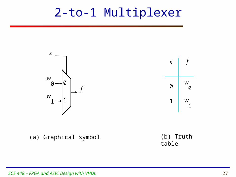
2-to-1 Multiplexer
(a) Graphical symbol (b) Truth table
0
1
fs
w0
w1
f
s
w0
w1
0
1

28ECE 448 – FPGA and ASIC Design with VHDL
VHDL code for a 2-to-1 Multiplexer
LIBRARY ieee ;USE ieee.std_logic_1164.all ;
ENTITY mux2to1 ISPORT ( w0, w1, s : IN STD_LOGIC ;
f : OUT STD_LOGIC ) ;END mux2to1 ;
ARCHITECTURE dataflow OF mux2to1 ISBEGIN
f <= w0 WHEN s = '0' ELSE w1 ;END dataflow ;

29ECE 448 – FPGA and ASIC Design with VHDL
Cascade of two multiplexers
s1
w3
w1
0
1
s2
w2
0
1 y

30ECE 448 – FPGA and ASIC Design with VHDL
VHDL code for a cascade of two multiplexers
LIBRARY ieee ;USE ieee.std_logic_1164.all ;
ENTITY mux_cascade ISPORT ( w1, w2, w3: IN STD_LOGIC ;
s1, s2 : IN STD_LOGIC ;f : OUT STD_LOGIC ) ;
END mux_cascade ;
ARCHITECTURE dataflow OF mux2to1 ISBEGIN
f <= w1 WHEN s1 = ‘1' ELSE w2 WHEN s2 = ‘1’ ELSE w3 ;END dataflow ;

31ECE 448 – FPGA and ASIC Design with VHDL
Operators
• Relational operators
• Logic and relational operators precedence
= /= < <= > >=
not= /= < <= > >=and or nand nor xor xnor
Highest
Lowest

32ECE 448 – FPGA and ASIC Design with VHDL
compare a = bc
Incorrect
… when a = b and c else …
equivalent to
… when (a = b) and c else …
Correct
… when a = (b and c) else …
Priority of logic and relational operators

33ECE 448 – FPGA and ASIC Design with VHDL
VHDL operators

34ECE 448 – FPGA and ASIC Design with VHDL
f
s 1
w 0
w 1
00
01
(b) Truth table
w 0
w 1
s 0
w 2
w 3
10
11
0
0
1
1
1
0
1
f s 1
0
s 0
w 2
w 3
(a) Graphic symbol
4-to-1 Multiplexer

35ECE 448 – FPGA and ASIC Design with VHDL
VHDL code for a 4-to-1 Multiplexer
LIBRARY ieee ;USE ieee.std_logic_1164.all ;
ENTITY mux4to1 ISPORT ( w0, w1, w2, w3 : IN STD_LOGIC ;
s : IN STD_LOGIC_VECTOR(1 DOWNTO 0) ;f : OUT STD_LOGIC ) ;
END mux4to1 ;
ARCHITECTURE dataflow OF mux4to1 ISBEGIN
WITH s SELECTf <= w0 WHEN "00",
w1 WHEN "01",w2 WHEN "10",w3 WHEN OTHERS ;
END dataflow ;

36ECE 448 – FPGA and ASIC Design with VHDL
Decoders

37ECE 448 – FPGA and ASIC Design with VHDL
2-to-4 Decoder
0
0
1
1
1
0
1
y 3
w 1
0
w 0
x x
1
1
0
1
1
En
0
0
1
0
0
y 2
0
1
0
0
0
y 1
1
0
0
0
0
y 0
0
0
0
1
0
w 1
En
y 3
w 0
y 2
y 1
y 0
(a) Truth table (b) Graphical symbol

38ECE 448 – FPGA and ASIC Design with VHDL
VHDL code for a 2-to-4 Decoder
LIBRARY ieee ;USE ieee.std_logic_1164.all ;
ENTITY dec2to4 ISPORT ( w : IN STD_LOGIC_VECTOR(1 DOWNTO 0) ;
En : IN STD_LOGIC ;y : OUT STD_LOGIC_VECTOR(3 DOWNTO 0) ) ;
END dec2to4 ;
ARCHITECTURE dataflow OF dec2to4 ISSIGNAL Enw : STD_LOGIC_VECTOR(2 DOWNTO 0) ;
BEGINEnw <= En & w ;WITH Enw SELECT
y <= “0001" WHEN "100","0010" WHEN "101","0100" WHEN "110",“1000" WHEN "111","0000" WHEN OTHERS ;
END dataflow ;

39ECE 448 – FPGA and ASIC Design with VHDL
Adders

40ECE 448 – FPGA and ASIC Design with VHDL
16-bit Unsigned Adder
16 16
X Y
16
CinCoutS

41ECE 448 – FPGA and ASIC Design with VHDL
Arithmetic Operators in VHDL (1)
To use basic arithmetic operations involving
std_logic_vectors you need to include the
following library packages:
LIBRARY ieee;USE ieee.std_logic_1164.all;USE ieee.std_logic_unsigned.all;orUSE ieee.std_logic_signed.all;

42ECE 448 – FPGA and ASIC Design with VHDL
Arithmetic Operators in VHDL (2)
You can use standard + and - operators
to perform addition and subtraction:
signal A : STD_LOGIC_VECTOR(3 downto 0); signal B : STD_LOGIC_VECTOR(3 downto 0); signal C : STD_LOGIC_VECTOR(3 downto 0);
……
C <= A + B;

43ECE 448 – FPGA and ASIC Design with VHDL
VHDL code for a 16-bit Unsigned Adder
LIBRARY ieee ;USE ieee.std_logic_1164.all ;USE ieee.std_logic_unsigned.all ;
ENTITY adder16 ISPORT ( Cin : IN STD_LOGIC ;
X, Y : IN STD_LOGIC_VECTOR(15 DOWNTO 0) ;S : OUT STD_LOGIC_VECTOR(15 DOWNTO 0) ;Cout : OUT STD_LOGIC ) ;
END adder16 ;
ARCHITECTURE dataflow OF adder16 IS SIGNAL Sum : STD_LOGIC_VECTOR(16 DOWNTO 0) ;
BEGINSum <= ('0' & X) + Y + Cin ;S <= Sum(15 DOWNTO 0) ;Cout <= Sum(16) ;
END dataflow ;

44ECE 448 – FPGA and ASIC Design with VHDL
Comparators

45ECE 448 – FPGA and ASIC Design with VHDL
4-bit Number Comparator
4
4
A
B
AeqB
AgtB
AltB
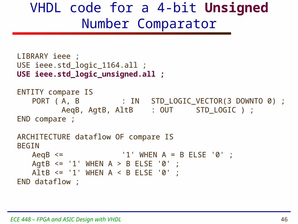
46ECE 448 – FPGA and ASIC Design with VHDL
VHDL code for a 4-bit Unsigned Number Comparator
LIBRARY ieee ;USE ieee.std_logic_1164.all ;USE ieee.std_logic_unsigned.all ;
ENTITY compare ISPORT ( A, B : IN STD_LOGIC_VECTOR(3 DOWNTO 0) ;
AeqB, AgtB, AltB : OUT STD_LOGIC ) ;END compare ;
ARCHITECTURE dataflow OF compare ISBEGIN
AeqB <= '1' WHEN A = B ELSE '0' ;AgtB <= '1' WHEN A > B ELSE '0' ;AltB <= '1' WHEN A < B ELSE '0' ;
END dataflow ;

47ECE 448 – FPGA and ASIC Design with VHDL
VHDL code for a 4-bit Signed Number Comparator
LIBRARY ieee ;USE ieee.std_logic_1164.all ;USE ieee.std_logic_signed.all ;
ENTITY compare ISPORT ( A, B : IN STD_LOGIC_VECTOR(3 DOWNTO 0) ;
AeqB, AgtB, AltB : OUT STD_LOGIC ) ;END compare ;
ARCHITECTURE dataflow OF compare ISBEGIN
AeqB <= '1' WHEN A = B ELSE '0' ;AgtB <= '1' WHEN A > B ELSE '0' ;AltB <= '1' WHEN A < B ELSE '0' ;
END dataflow ;

48ECE 448 – FPGA and ASIC Design with VHDL
Buffers

49ECE 448 – FPGA and ASIC Design with VHDL
(b) Equivalent circuit
(c) Truth table
x f
e
(a) A tri-state buffer
0 0 1 1
0 1 0 1
Z Z 0 1
f e x
x f
e = 0
e = 1x f
Tri-state Buffer
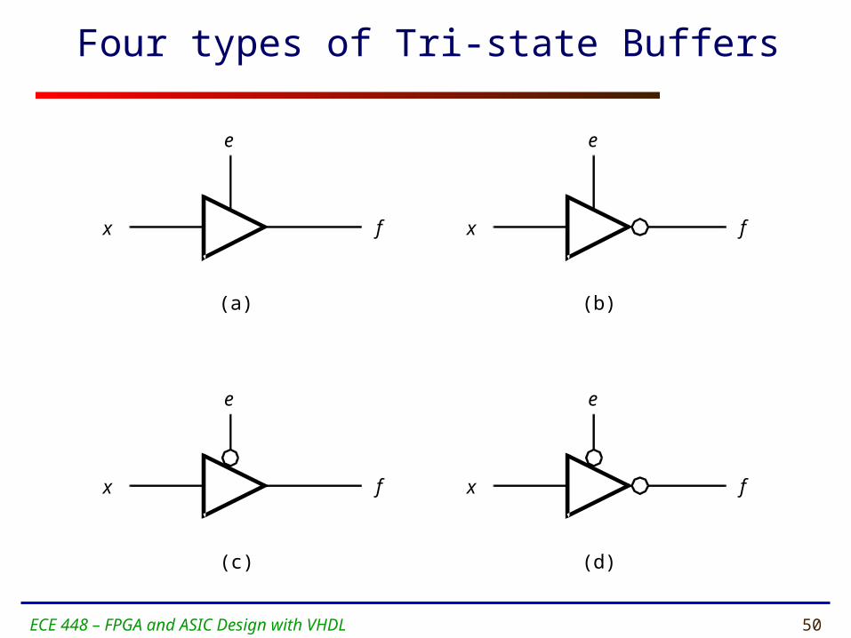
50ECE 448 – FPGA and ASIC Design with VHDL
x f
e
(b)
x f
e
(a)
x f
e
(c)
x f
e
(d)
Four types of Tri-state Buffers

51ECE 448 – FPGA and ASIC Design with VHDL
Tri-state Buffer – example (1)
LIBRARY ieee;
USE ieee.std_logic_1164.all;
ENTITY tri_state IS
PORT ( ena: IN STD_LOGIC;
input: IN STD_LOGIC;
output: OUT STD_LOGIC
);
END tri_state;

52ECE 448 – FPGA and ASIC Design with VHDL
Tri-state Buffer – example (2)
ARCHITECTURE dataflow OF tri_state IS
BEGIN
output <= input WHEN (ena = ‘1’) ELSE ‘Z’;
END dataflow;

53ECE 448 – FPGA and ASIC Design with VHDL
Encoders

54ECE 448 – FPGA and ASIC Design with VHDL
Priority Encoder
w 0
w 3
y 0
y 1
d001
010
w0 y1
d
y0
1 1
01
1
11
z
1xx
0
x
w1
01x
0
x
w2
001
0
x
w3
000
0
1
z
w 1
w 2

55ECE 448 – FPGA and ASIC Design with VHDL
VHDL code for a Priority Encoder
LIBRARY ieee ;USE ieee.std_logic_1164.all ;
ENTITY priority ISPORT ( w : IN STD_LOGIC_VECTOR(3 DOWNTO 0) ;
y : OUT STD_LOGIC_VECTOR(1 DOWNTO 0) ;z : OUT STD_LOGIC ) ;
END priority ;
ARCHITECTURE dataflow OF priority ISBEGIN
y <= "11" WHEN w(3) = '1' ELSE "10" WHEN w(2) = '1' ELSE"01" WHEN w(1) = '1' ELSE"00" ;
z <= '0' WHEN w = "0000" ELSE '1' ;END dataflow ;

56ECE 448 – FPGA and ASIC Design with VHDL
Describing
Combinational Logic
Using
Dataflow Design Style

57ECE 448 – FPGA and ASIC Design with VHDL
MLU Example

MLU Block Diagram
B
A
NEG_A
NEG_B
IN0
IN1
IN2
IN3
OUTPUT
SEL1SEL0
MUX_4_1
L0L1
NEG_Y
Y
Y1
A1
B1
MUX_0
MUX_1
MUX_2
MUX_3
0
1
0
1
0
1

59ECE 448 – FPGA and ASIC Design with VHDL
MLU: Entity Declaration
LIBRARY ieee;USE ieee.std_logic_1164.all;
ENTITY mlu IS PORT(
NEG_A : IN STD_LOGIC; NEG_B : IN STD_LOGIC; NEG_Y : IN STD_LOGIC; A : IN STD_LOGIC; B : IN STD_LOGIC; L1 : IN STD_LOGIC; L0 : IN STD_LOGIC; Y : OUT STD_LOGIC
);END mlu;

60ECE 448 – FPGA and ASIC Design with VHDL
MLU: Architecture Declarative Section
ARCHITECTURE mlu_dataflow OF mlu IS
SIGNAL A1 : STD_LOGIC;SIGNAL B1 : STD_LOGIC;SIGNAL Y1 : STD_LOGIC;SIGNAL MUX_0 : STD_LOGIC;SIGNAL MUX_1 : STD_LOGIC;SIGNAL MUX_2 : STD_LOGIC;SIGNAL MUX_3 : STD_LOGIC;SIGNAL L: STD_LOGIC_VECTOR(1 DOWNTO 0);

61ECE 448 – FPGA and ASIC Design with VHDL
MLU - Architecture BodyBEGIN
A1<= NOT A WHEN (NEG_A='1') ELSEA;
B1<= NOT B WHEN (NEG_B='1') ELSE B;
Y <= NOT Y1 WHEN (NEG_Y='1') ELSEY1;
MUX_0 <= A1 AND B1;MUX_1 <= A1 OR B1;MUX_2 <= A1 XOR B1;MUX_3 <= A1 XNOR B1;
L <= L1 & L0;
with (L) select Y1 <= MUX_0 WHEN "00",
MUX_1 WHEN "01", MUX_2 WHEN "10",
MUX_3 WHEN OTHERS;
END mlu_dataflow;

62ECE 448 – FPGA and ASIC Design with VHDL
Logic Implied Most Often by
Conditional and Selected
Concurrent Signal
Assignments

63ECE 448 – FPGA and ASIC Design with VHDL
Data-flow VHDL
• concurrent signal assignment ()• conditional concurrent signal assignment (when-else)• selected concurrent signal assignment (with-select-when)• generate scheme for equations (for-generate)
Major instructions
Concurrent statements

64ECE 448 – FPGA and ASIC Design with VHDL
Conditional concurrent signal assignment
target_signal <= value1 when condition1 else value2 when condition2 else . . . valueN-1 when conditionN-1 else valueN;
When - Else

65ECE 448 – FPGA and ASIC Design with VHDL
Most often implied structure
target_signal <= value1 when condition1 else value2 when condition2 else . . . valueN-1 when conditionN-1 else valueN;
When - Else
.…Value N
Value N-1
Condition N-1
Condition 2
Condition 1
Value 2
Value 1
Target Signal
…0
1
0
1
0
1

66ECE 448 – FPGA and ASIC Design with VHDL
Data-flow VHDL
• concurrent signal assignment ()• conditional concurrent signal assignment (when-else)• selected concurrent signal assignment (with-select-when)• generate scheme for equations (for-generate)
Major instructions
Concurrent statements

67ECE 448 – FPGA and ASIC Design with VHDL
Selected concurrent signal assignment
with choice_expression select target_signal <= expression1 when choices_1, expression2 when choices_2, . . . expressionN when choices_N;
With –Select-When

68ECE 448 – FPGA and ASIC Design with VHDL
Most Often Implied Structure
with choice_expression select target_signal <= expression1 when choices_1, expression2 when choices_2, . . . expressionN when choices_N;
With –Select-When
choices_1
choices_2
choices_N
expression1
target_signal
choice expression
expression2
expressionN

69ECE 448 – FPGA and ASIC Design with VHDL
Allowed formats of choices_k
WHEN value
WHEN value_1 | value_2 | .... | value N
WHEN OTHERS

70ECE 448 – FPGA and ASIC Design with VHDL
Allowed formats of choice_k - example
WITH sel SELECT
y <= a WHEN "000",
c WHEN "001" | "111",
d WHEN OTHERS;