Embed Size (px)
Citation preview
Chakib Alaoui
International Journal of Engineering (IJE), Volume (5) : Issue (1) : 2011 102
Design and Simulation of a Modified Architecture of Carry Save Adder
Chakib Alaoui [email protected] College of Computers and Information Technology Taif University, KSA
Abstract
This paper presents a technology-independent design and simulation of a modified architecture of the Carry-Save Adder. This architecture is shown to produce the result of the addition fast and by requiring a minimum number of logic gates. Binary addition is carried out by a series of XOR, AND and Shift-left operations. These operations are terminated with a completion signal indicating that the result of the addition is obtained. Because the number of shift operations carried out varies from 0 to n for n-bit addends, a behavioral model was developed in which all the possible addends having 2- to 15-bits were applied. A mathematical model was deducted from the data and used to predict the average number of shift required for standard binary numbers such as 32, 64 or 128-bits. 4-bit prototypes of this adder were designed and simulated in both synchronous and asynchronous modes of operation.
Keywords: Carry Save Adder, Synchronous Adder, Asynchronous Adder, VHDL Simulation.
1. INTRODUCTION Addition is the most important operation in any digital system. All other arithmetic operations, such as subtraction, multiplication and division are deeply related to the addition; hence, the design of a fast, accurate and low power binary adder translates to a gain in simulation speed and an increase in battery life for portable computing systems [1-3]. Many circuits for binary arithmetic addition exists, such as the ripple carry adder, the carry skip adder, the carry look-ahead adder, the carry select adder, Manchester chain adder, prefix adder among others [4-8]. The performance of these adders has been evaluated in several publications in terms of speed, area and power consumption [4-8]. Arithmetic transformations using carry-save adders (CSAs) have been exploited recently in [9]. Variations of the techniques proposed in [9] have also been reported [10-13]. Carry-save transformations across non-addition operators were proposed in [10]. The timing and area trade-offs of carry-save implementation for multiple addition trees were exploited in [11]. However, all these transformation techniques [9-11] optimize combinatorial circuits only. They are obviously limited by the register boundaries and cannot be applied to optimize synchronous data-path circuits. Arithmetic operations other than addition have been implemented by using CSAs in [12-14]. This paper presents a new modification to the carry-save-adder (CSA) for fast addition. An algorithm was first developed and checked with several arithmetic additions to verify its correctness. Since the number of binary operations needed to compute the addition varies from 0 to n for n-bit addends, a behavioral model was developed in Matlab in order to check all possible binary operations that exist between two n-bit binary numbers. Finally, 4-bit synchronous and asynchronous prototypes were designed and implemented by using Quartus II design Software. These prototypes were chosen to be technology-independent at first. They can be re-simulated by using any technology process such as 0.18µm, 0.13µm or others.
Chakib Alaoui
International Journal of Engineering (IJE), Volume (5) : Issue (1) : 2011 103
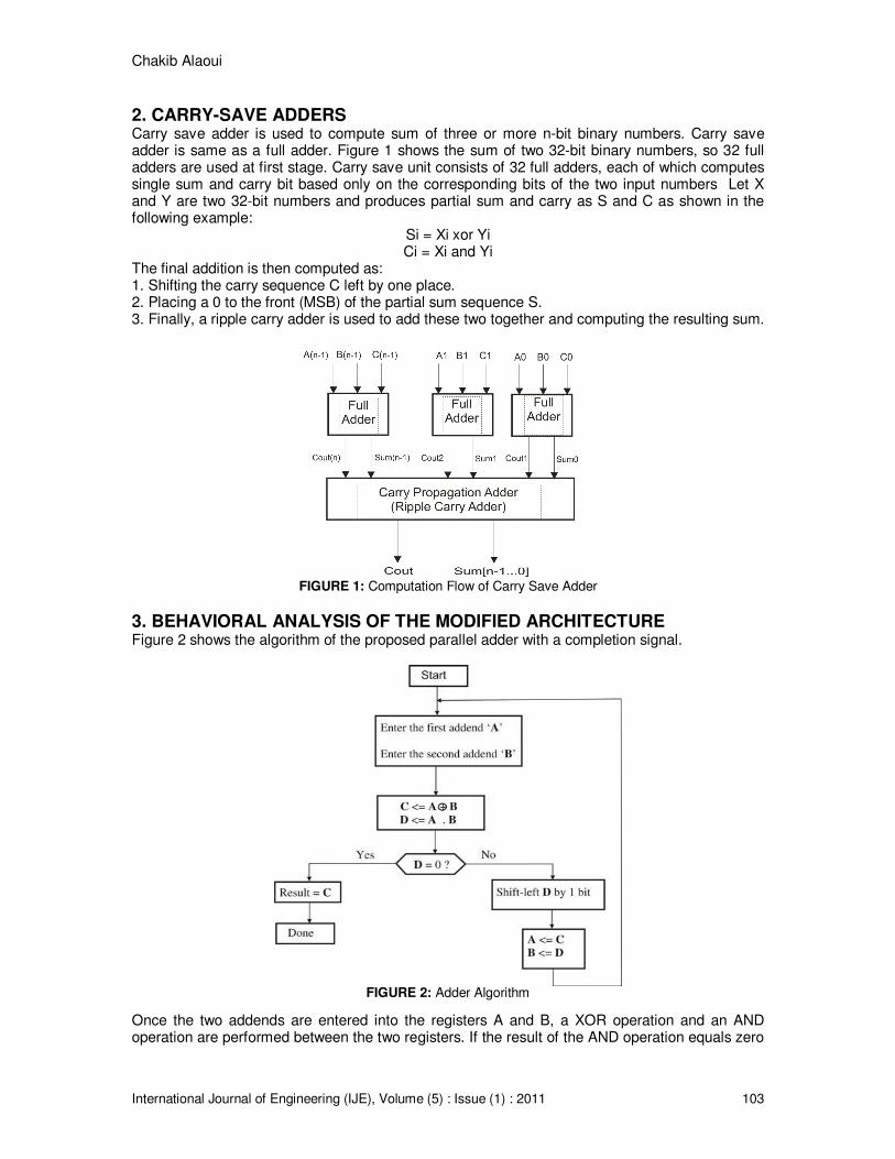
2. CARRY-SAVE ADDERS Carry save adder is used to compute sum of three or more n-bit binary numbers. Carry save adder is same as a full adder. Figure 1 shows the sum of two 32-bit binary numbers, so 32 full adders are used at first stage. Carry save unit consists of 32 full adders, each of which computes single sum and carry bit based only on the corresponding bits of the two input numbers Let X and Y are two 32-bit numbers and produces partial sum and carry as S and C as shown in the following example:
Si = Xi xor Yi Ci = Xi and Yi
The final addition is then computed as: 1. Shifting the carry sequence C left by one place. 2. Placing a 0 to the front (MSB) of the partial sum sequence S. 3. Finally, a ripple carry adder is used to add these two together and computing the resulting sum.
FIGURE 1: Computation Flow of Carry Save Adder
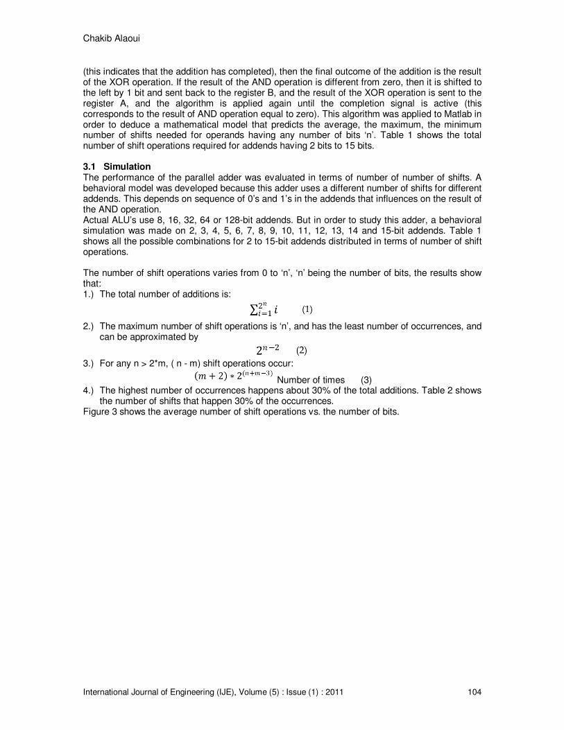
3. BEHAVIORAL ANALYSIS OF THE MODIFIED ARCHITECTURE Figure 2 shows the algorithm of the proposed parallel adder with a completion signal.
FIGURE 2: Adder Algorithm
Once the two addends are entered into the registers A and B, a XOR operation and an AND operation are performed between the two registers. If the result of the AND operation equals zero
Chakib Alaoui
International Journal of Engineering (IJE), Volume (5) : Issue (1) : 2011 104
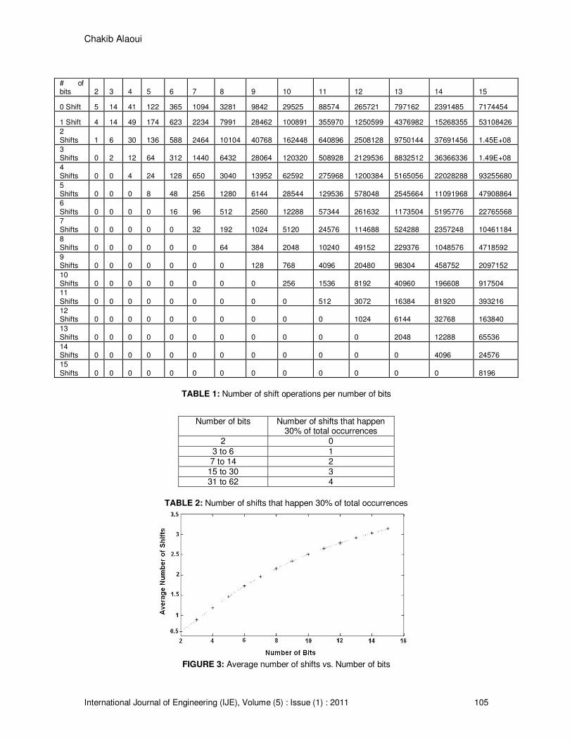
(this indicates that the addition has completed), then the final outcome of the addition is the result of the XOR operation. If the result of the AND operation is different from zero, then it is shifted to the left by 1 bit and sent back to the register B, and the result of the XOR operation is sent to the register A, and the algorithm is applied again until the completion signal is active (this corresponds to the result of AND operation equal to zero). This algorithm was applied to Matlab in order to deduce a mathematical model that predicts the average, the maximum, the minimum number of shifts needed for operands having any number of bits ‘n’. Table 1 shows the total number of shift operations required for addends having 2 bits to 15 bits. 3.1 Simulation The performance of the parallel adder was evaluated in terms of number of number of shifts. A behavioral model was developed because this adder uses a different number of shifts for different addends. This depends on sequence of 0’s and 1’s in the addends that influences on the result of the AND operation. Actual ALU’s use 8, 16, 32, 64 or 128-bit addends. But in order to study this adder, a behavioral simulation was made on 2, 3, 4, 5, 6, 7, 8, 9, 10, 11, 12, 13, 14 and 15-bit addends. Table 1 shows all the possible combinations for 2 to 15-bit addends distributed in terms of number of shift operations. The number of shift operations varies from 0 to ‘n’, ‘n’ being the number of bits, the results show that: 1.) The total number of additions is:
2.) The maximum number of shift operations is ‘n’, and has the least number of occurrences, and
can be approximated by
3.) For any n > 2*m, ( n - m) shift operations occur:
Number of times (3) 4.) The highest number of occurrences happens about 30% of the total additions. Table 2 shows
the number of shifts that happen 30% of the occurrences. Figure 3 shows the average number of shift operations vs. the number of bits.
Chakib Alaoui
International Journal of Engineering (IJE), Volume (5) : Issue (1) : 2011 105
# of bits 2 3 4 5 6 7 8 9 10 11 12 13 14 15
0 Shift 5 14 41 122 365 1094 3281 9842 29525 88574 265721 797162 2391485 7174454
1 Shift 4 14 49 174 623 2234 7991 28462 100891 355970 1250599 4376982 15268355 53108426
2 Shifts 1 6 30 136 588 2464 10104 40768 162448 640896 2508128 9750144 37691456 1.45E+08
3 Shifts 0 2 12 64 312 1440 6432 28064 120320 508928 2129536 8832512 36366336 1.49E+08
4 Shifts 0 0 4 24 128 650 3040 13952 62592 275968 1200384 5165056 22028288 93255680
5 Shifts 0 0 0 8 48 256 1280 6144 28544 129536 578048 2545664 11091968 47908864
6 Shifts 0 0 0 0 16 96 512 2560 12288 57344 261632 1173504 5195776 22765568
7 Shifts 0 0 0 0 0 32 192 1024 5120 24576 114688 524288 2357248 10461184
8 Shifts 0 0 0 0 0 0 64 384 2048 10240 49152 229376 1048576 4718592
9 Shifts 0 0 0 0 0 0 0 128 768 4096 20480 98304 458752 2097152
10 Shifts 0 0 0 0 0 0 0 0 256 1536 8192 40960 196608 917504
11 Shifts 0 0 0 0 0 0 0 0 0 512 3072 16384 81920 393216
12 Shifts 0 0 0 0 0 0 0 0 0 0 1024 6144 32768 163840
13 Shifts 0 0 0 0 0 0 0 0 0 0 0 2048 12288 65536
14 Shifts 0 0 0 0 0 0 0 0 0 0 0 0 4096 24576
15 Shifts 0 0 0 0 0 0 0 0 0 0 0 0 0 8196
TABLE 1: Number of shift operations per number of bits
Number of bits Number of shifts that happen 30% of total occurrences
2 0
3 to 6 1 7 to 14 2
15 to 30 3 31 to 62 4
TABLE 2: Number of shifts that happen 30% of total occurrences
FIGURE 3: Average number of shifts vs. Number of bits
Chakib Alaoui
International Journal of Engineering (IJE), Volume (5) : Issue (1) : 2011 106
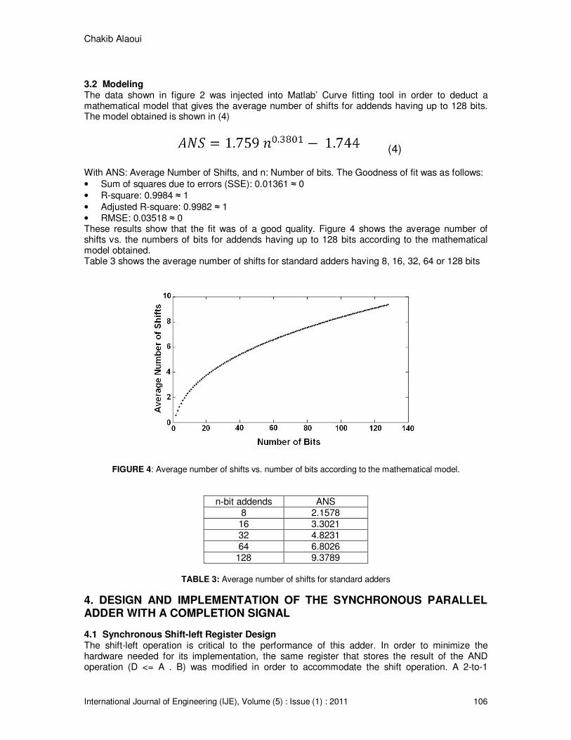
3.2 Modeling The data shown in figure 2 was injected into Matlab’ Curve fitting tool in order to deduct a mathematical model that gives the average number of shifts for addends having up to 128 bits. The model obtained is shown in (4)
(4) With ANS: Average Number of Shifts, and n: Number of bits. The Goodness of fit was as follows:
• Sum of squares due to errors (SSE): 0.01361 ≈ 0
• R-square: 0.9984 ≈ 1
• Adjusted R-square: 0.9982 ≈ 1 • RMSE: 0.03518 ≈ 0 These results show that the fit was of a good quality. Figure 4 shows the average number of shifts vs. the numbers of bits for addends having up to 128 bits according to the mathematical model obtained. Table 3 shows the average number of shifts for standard adders having 8, 16, 32, 64 or 128 bits
FIGURE 4: Average number of shifts vs. number of bits according to the mathematical model.
n-bit addends ANS 8 2.1578
16 3.3021 32 4.8231 64 6.8026
128 9.3789
TABLE 3: Average number of shifts for standard adders
4. DESIGN AND IMPLEMENTATION OF THE SYNCHRONOUS PARALLEL ADDER WITH A COMPLETION SIGNAL
4.1 Synchronous Shift-left Register Design The shift-left operation is critical to the performance of this adder. In order to minimize the hardware needed for its implementation, the same register that stores the result of the AND operation (D <= A . B) was modified in order to accommodate the shift operation. A 2-to-1

Chakib Alaoui
International Journal of Engineering (IJE), Volume (5) : Issue (1) : 2011 107
multiplexer was added to each D flip-flop. The selection bit of these multiplexers allow either the loading of D when Load/Shift = ‘1’ or the shift to the left of D by 1 bit when Load/Shift =’0’. These actions happen at the rising edge of the clock since this circuit works in synchronous mode of operation. Figure 5 shows the logic circuit for the synchronous shift-left operation.
FIGURE 5: Shift-Left Register Logic Circuit
4.2 Shift-left Register Simulation The logic circuit of figure 4 was simulated with Quartus II design software. Figure 6 shows the output waveforms. For testing purposes, a binary data of D[3..0]=1111 was sent to the register D. This value was first loaded into the register (Load/Shift = ‘1’), then it was shifted to the left by 1 bit after each rising edge of the clock. Table 4 shows the timing and the bit values of the D registers.
FIGURE 6: Output waveforms of the Shift-left register
Timing Action Load/Shift D4&D[3..0] t0 Load data 1 (Load) 01111 t1 Shit-left by 1 bit 0 (Shift) 11110
t2 Shit-left by 1 bit 0 (Shift) 11100 t3 Shit-left by 1 bit 0 (Shift) 11000 t4 Shit-left by 1 bit 0 (Shift) 10000 t5 Shit-left by 1 bit 0 (Shift) 00000
TABLE 4: Timing of shift-left logic circuit
4.3 Synchronous Parallel Adder Design Figure 6 shows the logic circuit of the proposed synchronous adder. For simulation purposes, the circuit was designed for 4-bit addends. The same principle can be easily extended to 32, 64-bit or more addends. An extra bit is needed as the carry bit.
Chakib Alaoui
International Journal of Engineering (IJE), Volume (5) : Issue (1) : 2011 108
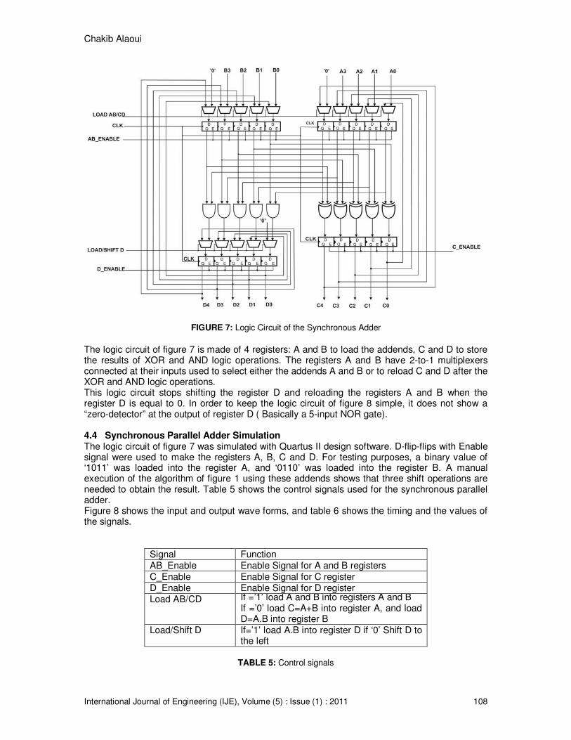
FIGURE 7: Logic Circuit of the Synchronous Adder
The logic circuit of figure 7 is made of 4 registers: A and B to load the addends, C and D to store the results of XOR and AND logic operations. The registers A and B have 2-to-1 multiplexers connected at their inputs used to select either the addends A and B or to reload C and D after the XOR and AND logic operations. This logic circuit stops shifting the register D and reloading the registers A and B when the register D is equal to 0. In order to keep the logic circuit of figure 8 simple, it does not show a “zero-detector” at the output of register D ( Basically a 5-input NOR gate). 4.4 Synchronous Parallel Adder Simulation The logic circuit of figure 7 was simulated with Quartus II design software. D-flip-flips with Enable signal were used to make the registers A, B, C and D. For testing purposes, a binary value of ‘1011’ was loaded into the register A, and ‘0110’ was loaded into the register B. A manual execution of the algorithm of figure 1 using these addends shows that three shift operations are needed to obtain the result. Table 5 shows the control signals used for the synchronous parallel adder. Figure 8 shows the input and output wave forms, and table 6 shows the timing and the values of the signals.
Signal Function AB_Enable Enable Signal for A and B registers C_Enable Enable Signal for C register D_Enable Enable Signal for D register Load AB/CD If =’1’ load A and B into registers A and B
If =’0’ load C=A+B into register A, and load D=A.B into register B
Load/Shift D If=’1’ load A.B into register D if ‘0’ Shift D to the left
TABLE 5: Control signals
Chakib Alaoui
International Journal of Engineering (IJE), Volume (5) : Issue (1) : 2011 109
FIGURE 8: Wave forms of the Synchronous Adder
Timing Action Values
t1 Load A, Load B A = ’1011’ B = ’0110’ t2 C <= A + B, D <= A . B C = ’01101’ D = ’00010’
t3 Shift D to the left D = ’00100’ t4 Load C into A, Load D into B A = ’01101’ B = ’00100’ t5 C <= A + B, D <= A . B C = ’01001’ D = ’00100’ t6 Shift D to the left D = ’01000’
t7 Load C into A, Load D into B A = ’01001’ B = ’01000’ t8 C <= A + B, D <= A . B C = ’00001’ D = ’01000’ t9 Shift D to the left D = ’10000’
t10 Load C into A, Load D into B A = ’00001’ B = ’10000’ t11 C <= A + B, D <= A . B C = ’10001’ D = ’00000’
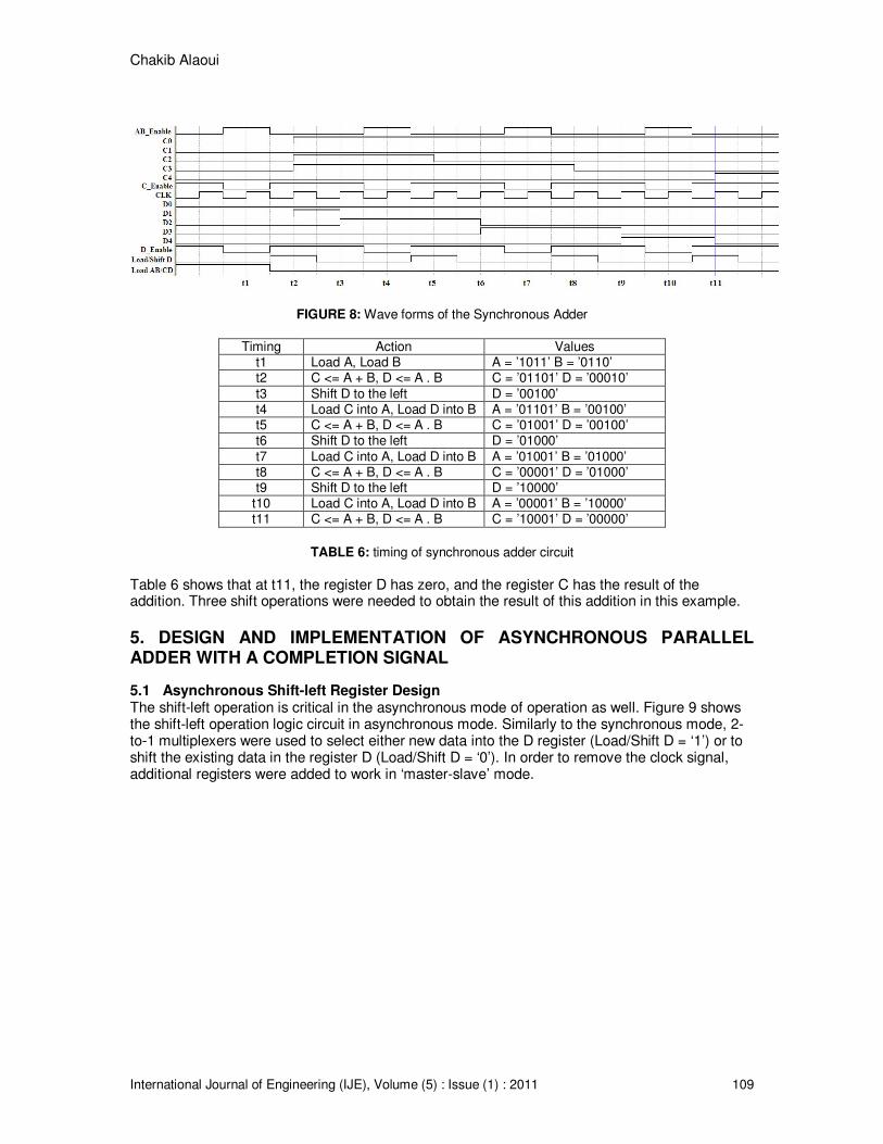
TABLE 6: timing of synchronous adder circuit
Table 6 shows that at t11, the register D has zero, and the register C has the result of the addition. Three shift operations were needed to obtain the result of this addition in this example.
5. DESIGN AND IMPLEMENTATION OF ASYNCHRONOUS PARALLEL ADDER WITH A COMPLETION SIGNAL
5.1 Asynchronous Shift-left Register Design The shift-left operation is critical in the asynchronous mode of operation as well. Figure 9 shows the shift-left operation logic circuit in asynchronous mode. Similarly to the synchronous mode, 2-to-1 multiplexers were used to select either new data into the D register (Load/Shift D = ‘1’) or to shift the existing data in the register D (Load/Shift D = ‘0’). In order to remove the clock signal, additional registers were added to work in ‘master-slave’ mode.

Chakib Alaoui
International Journal of Engineering (IJE), Volume (5) : Issue (1) : 2011 110
FIGURE 9: Asynchronous Shift Register
5.2 Asynchronous Shift-left Register Simulation Figure 9 shows the Quartus II simulation of the asynchronous shift register of figure 8. For testing purposes, a value of D=[1111] was first loaded into the register D (t1 in figure 11, Load/Shift = ‘1’). In order to shift the data by 1 bit to the left, Load/Shift = ‘0’, and send an impulse to the register preD (master) ‘1’ →’0’, followed by a second impulse to the register D (slave) ‘0’ →’1’. This is illustrated at (t2, t3), (t4, t5), (t6, t7) etc. in figure 10. Table 7 shows the asynchronous shift register simulation results and control signals in greater detail.
FIGURE 10: Asynchronous Shift Register
Timing Action Control Signals D4&D[3..0] t0→t1 Load data Load/Shift D <= ’1’ preD_Enable <= ‘1’→‘0’
D_Enable <= ‘0’→‘1’ 01111
t2 →t3 Shit-left by 1 bit Load/Shift D <= ’0’ preD_Enable <= ‘1’→‘0’ D_Enable <= ‘0’→‘1’
11110
t4 →t5 Shit-left by 1 bit Load/Shift D <= ’0’ preD_Enable <= ‘1’→‘0’ D_Enable <= ‘0’→‘1’
11100
t6 →t7 Shit-left by 1 bit Load/Shift D <= ’0’ preD_Enable <= ‘1’→‘0’ D_Enable <= ‘0’→‘1’
11000
t8 →t9 Shit-left by 1 bit Load/Shift D <= ’0’ preD_Enable <= ‘1’→‘0’ D_Enable <= ‘0’→‘1’
10000
t10 →t11 Shit-left by 1 bit Load/Shift D <= ’0’ preD_Enable <= ‘1’→‘0’ D_Enable <= ‘0’→‘1’
00000
TABLE 7: Timing of shift-left logic circuit
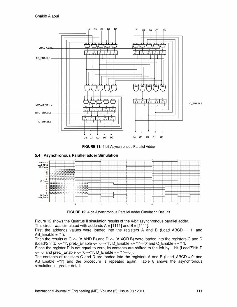
5.3 Asynchronous Parallel Adder Design Figure 10 shows the logic circuit for the 4-bit asynchronous adder. This logic circuit is very similar to its synchronous version. It contains four registers A, B, C and D. 4-bit addends were used in figure 11, plus an extra bit as carry.
Chakib Alaoui
International Journal of Engineering (IJE), Volume (5) : Issue (1) : 2011 111
FIGURE 11: 4-bit Asynchronous Parallel Adder
5.4 Asynchronous Parallel adder Simulation
FIGURE 12: 4-bit Asynchronous Parallel Adder Simulation Results
Figure 12 shows the Quartus II simulation results of the 4-bit asynchronous parallel adder. This circuit was simulated with addends A = [1111] and B = [1111]. First the addends values were loaded into the registers A and B (Load_ABCD = ‘1’ and AB_Enable = ‘1’). Then the results of C <= (A AND B) and D <= (A XOR B) were loaded into the registers C and D (Load/ShiftD <= ‘1’, preD_Enable <= ‘0’→’1’, D_Enable <= ‘1’→’0’ and C_Enable <= ‘1’). Since the register D is not equal to zero, its contents are shifted to the left by 1 bit (Load/Shift D <= ‘0’ and preD_Enable <= ‘0’→’1’, D_Enable <= ‘1’→’0’). The contents of registers C and D are loaded into the registers A and B (Load_ABCD =‘0’ and AB_Enable =’1’) and the procedure is repeated again. Table 8 shows the asynchronous simulation in greater detail.
Chakib Alaoui
International Journal of Engineering (IJE), Volume (5) : Issue (1) : 2011 112
Timing Action Control Signals Values
0 → t1 Load A, Load B AB_Enable <= ‘1’, Load_ABCD <= ‘1’ A = ’01111’, B = ’01111’ t1 → t2 C <= A + B, D <= A . B Load/Shift D <= ‘1’, C_Enable <= ‘1’
preD_Enable <= ‘1’→’0’, D_Enable <= ‘0’ →’1’ C = ’00000’, D = ’01111’
t2 → t3 Shift D to the left Load/Shift D <= ‘0’, preD_Enable <= ‘1’→’0’ D_Enable <= ‘0’ →’1’
D = ’11110’
t3 → t4 Load C into A, Load D into B
Load_ABCD <= ‘0’, AB_Enable <= ‘1’ A = ’00000’, B = ’11110’
t4 → t5 C <= A + B, D <= A . B Load/Shift D <= ‘1’, C_Enable <= ‘1’ preD_Enable <= ‘1’→’0’, D_Enable <= ‘0’ →’1’
C = ’11110’, D = ’00000’
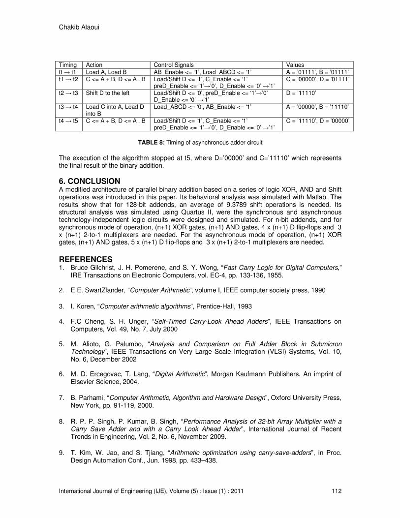
TABLE 8: Timing of asynchronous adder circuit
The execution of the algorithm stopped at t5, where D=’00000’ and C=’11110’ which represents the final result of the binary addition.
6. CONCLUSION A modified architecture of parallel binary addition based on a series of logic XOR, AND and Shift operations was introduced in this paper. Its behavioral analysis was simulated with Matlab. The results show that for 128-bit addends, an average of 9.3789 shift operations is needed. Its structural analysis was simulated using Quartus II, were the synchronous and asynchronous technology-independent logic circuits were designed and simulated. For n-bit addends, and for synchronous mode of operation, (n+1) XOR gates, (n+1) AND gates, 4 x (n+1) D flip-flops and 3 x (n+1) 2-to-1 multiplexers are needed. For the asynchronous mode of operation, (n+1) XOR gates, (n+1) AND gates, 5 x (n+1) D flip-flops and 3 x (n+1) 2-to-1 multiplexers are needed.
REFERENCES 1. Bruce Gilchrist, J. H. Pomerene, and S. Y. Wong, “Fast Carry Logic for Digital Computers,”
IRE Transactions on Electronic Computers, vol. EC-4, pp. 133-136, 1955.
2. E.E. SwartZlander, “Computer Arithmetic”, volume I, IEEE computer society press, 1990
3. I. Koren, “Computer arithmetic algorithms”, Prentice-Hall, 1993
4. F.C Cheng, S. H. Unger, “Self-Timed Carry-Look Ahead Adders”, IEEE Transactions on Computers, Vol. 49, No. 7, July 2000
5. M. Alioto, G. Palumbo, “Analysis and Comparison on Full Adder Block in Submicron Technology”, IEEE Transactions on Very Large Scale Integration (VLSI) Systems, Vol. 10, No. 6, December 2002
6. M. D. Ercegovac, T. Lang, “Digital Arithmetic”, Morgan Kaufmann Publishers. An imprint of
Elsevier Science, 2004.
7. B. Parhami, “Computer Arithmetic, Algorithm and Hardware Design”, Oxford University Press, New York, pp. 91-119, 2000.
8. R. P. P. Singh, P. Kumar, B. Singh, “Performance Analysis of 32-bit Array Multiplier with a Carry Save Adder and with a Carry Look Ahead Adder”, International Journal of Recent Trends in Engineering, Vol. 2, No. 6, November 2009.
9. T. Kim, W. Jao, and S. Tjiang, “Arithmetic optimization using carry-save-adders”, in Proc. Design Automation Conf., Jun. 1998, pp. 433–438.
Chakib Alaoui
International Journal of Engineering (IJE), Volume (5) : Issue (1) : 2011 113
10. T. Kim and J. Um, “A timing-driven synthesis of arithmetic circuits using carry-save-adders”, in Proc. Asia and South Pacific Design Automation Conf., Jan. 2000, pp. 313–316.
11. Y. Kim and T. Kim, “An accurate exploration of timing and area trade-offs in arithmetic
optimization using carry-save adder cells”, in Proc. Midwest Symposium on Circuit and Systems, Aug. 2000.
12. T. Kim, W. Jao,an d S. Tjiang,“Circuit Optimization using Carry-Save-Adder Cells”, IEEE TCAD, October 1998.
13. J. Um, T. Kim, C. L. Liu, “Optimal Allocation of Carry-Save-Adders in Arithmetic Optimization”, Proc. ICCAD, 1999.
14. B.Ramkumar, H. M Kittur, P.Mahesh Kannan, “ASIC implementation of Modified Faster Carry Save Adder”. European Journal of Scientific Research. ISSN 1450-216X, Vol.42 No.1, 2010, pp.53-58.


![M05 arith1.ppt [호환 모드] · 2016-10-31 · Ripple Carry Adder-4-bit ripple carry adder-LSB에서발생된carry가MSB까지전파된후에야sum 계산완료-Carry의전파가adder의계산시간결정](https://img.pdfslide.us/doc/110x75/5e6dfaba8472c611153db48f/m05-eeoe-2016-10-31-ripple-carry-adder-4-bit-ripple-carry-adder-lsboeeoefeoecarryemsbeoeoeoeeoesum.jpg)