Warped-Compression: Enabling Power Efficient GPUs through Register Compression
Sangpil Lee t Keunsoo Kim t Gunjae Koo+ tYonsei University
Hyeran leon+ Won Woo Rot Murali Annavaram+
+University of Southern California {madfish,keunsoo.kim,wro}@yonsei.ac.kr
Abstract This paper presents Warped-Compression, a warp-level
register compression scheme for reducing GPU power consumption. This work is motivated by the observation that the register values of threads within the same warp are similar, namely the arithmetic differences between two successive thread registers is small. Removing data redundancy of register values through register compression reduces the effective register width, thereby enabling power reduction opportunities. GPU register files are huge as they are necessary to keep concurrent execution contexts and to enable fast context switching. As a result register file consumes a large fraction of the total GPU chip power. GPU design trends show that the register file size will continue to increase to enable even more thread level parallelism. To reduce register file data redundancy warped-compression uses low-cost and implementationefficient base-delta-immediate (BDI) compression scheme, that takes advantage of banked register file organization used in GP Us. Since threads within a warp write values with strong similarity, BDI can quickly compress and decompress by selecting either a single register, or one of the register banks, as the primary base and then computing delta values of all the other registers, or banks. Warped-compression can be used to reduce both dynamic and leakage power. By compressing register values, each warp-level register access activates fewer register banks, which leads to reduction in dynamic power. When fewer banks are used to store the register content, leakage power can be reduced by power gating the unused banks. Evaluation results show that register compression saves 25%
of the total register file power consumption.
1. Introduction
GPUs are designed as throughput-oriented processors, which
rely on massive thread-level parallelism (TLP) to improve
Permission to make digital or hard copies of all or part of this work for
personal or classroom use is granted without fee provided that copies are not made or distributed for profit or commercial advantage and that copies bear this notice and the full citation on the first page. Copyrights for components of this work owned by others than ACM must be honored. Abstracting with credit is permitted. To copy otherwise, or republish, to post on servers or to redistribute to lists, requires prior specific permission and/or a fee. Request permissions from [email protected].
ISCA '15, June 13-17, 2015, Portland, OR, USA
© 20 15 ACM. ISBN 978-1-4503-3402-0/15/06$15.00 001: http://dx.doi.org/lO. 1145/2749469.2750417
502
{gunjae.koo,hyeranje,annavara}@usc.edu
computational throughput. Compared to multi-threaded CPUs
that support only a few hardware thread contexts, GPUs main
tain hundreds or even thousands of active threads . To effec
tively manage massive number of threads, a set of threads
are grouped into a warp (also called wavefront) . All threads
in a warp execute instructions in lock-step, which is called
single-instruction multiple-thread (SIMT) execution model [3] .
GPU evolution over generations has shown that the number of
execution units has been steadily increasing. To fully utilize
the execution units , the number of concurrent thread contexts
has also increased [8 , 7, 6] .
To enable fast context switch between threads, GPUs main
tain all active thread contexts in a large register file. The size
of the register file in GPUs is much larger than that of CPUs .
For instance, the NVIDIA Maxwell GPU has 64K 32-bit reg
isters per each streaming multiprocessor (SM) [6] , which is
much larger compared to 336 physical registers per core on
Intel Haswell CPU [26] .
Given their huge size, register file contributes up to
1 5 % of the total GPU chip power even in older generation
GPUs [35, 36] . There have been two approaches to save reg
ister file power consumption. The first approach turns otl
unused part of the register file to save both leakage and dy
namic power, and places used registers in drowsy state to
reduce leakage power. This approach exploits the observa
tion that some applications utilize only a fraction of the entire
register file or have large register inter-access time [9] . The
second approach to optimize dynamic power is based on the
register use locality. For instance, register file cache [2 1 ] uses
a small cache to capture register access locality thereby reduc
ing frequent accesses to the large register file banks . In [50] ,
the authors proposed a register file hierarchy to store a small
subset of registers in an SRAM while a lower power DRAM
stores the larger register file content.
This paper explores and exploits a different property of
register files, namely value similarity. In the SIMT execu
tion model since all threads within a warp execute the same
instruction, access to register file is also performed at warp
granularity. Because a warp consists of dozens of threads that
are identified using consecutive thread indices, many GPU
programming approaches use thread index to access and ma
nipulate data. As such many computations that rely on thread
index also operate on register data that exhibit strong value
similarity. Note that throughout this work we use the simple
metric of arithmetic distance to measure value similarity. An
arithmetic distance of n indicates that two values differ by
1nl- Even though register values across threads in a warp are
similar each thread register stores the entire redundant value.
Repeatedly storing, reading, and writing redundant data is one
source of power inefficiency that this work addresses .
Prior works [ 1 6, 17 , 30, 33] have also used the notion of
value similarity. The authors in [ 1 6] defined the notion of
value structure to capture scenarios where different threads
within a warp execute on input operands that can be described
as a simple function of thread ID and block ID. Value structure
can then be exploited for improving memory storage effi
ciency [ 17 ] . The authors in [30] exploited this value structure
further to create a separate affine functional unit that performs
more power efficient computations when a warp instruction
exhibits value structure. They also proposed hardware sup
port for branch instruction execution in the presence of value
structure to reduce the cost of branch resolution latency.
Inspired by these prior studies, this paper takes an orthog
onal approach to exploit value similarity to improve register
file power consumption. It proposes warped-compression, a
compression scheme for GPU register files based on the simi
larity of register values. Compression enables both dynamic
and leakage power reduction. Dynamic power is reduced by
decreasing the access count to each register bank by compress
ing the operand data into fewer physical register banks . Fur
thermore, dynamic power is reduced because the compressed
register read and write operations activate fewer bitlines in the
register file and fewer bits are moved across the wires between
register file and execution unit where the data is processed.
As has been shown in several studies [29, 1 8 , 3 1 , 42] , data
movement is as power hungry as computation. For instance
in [29] the authors showed that moving three 64-bit inputs
operand from registers to execution unit burns as much energy
as doing a double precision floating point operation. Leakage
power also can be reduced when using a narrow width banked
register file organization as is the case with GPUs. When a
wide register can be compressed to be stored in fewer register
banks, there are opportunities to power gate an entire register
bank.
We summarize the contributions of the paper as follows .
• We characterize value similarity of the registers at the gran
ularity of a warp access. Our findings show that threads
within a warp read and write values with small arithmetic
difference, particularly when the warp is in a non-divergent
code section, but the value similarity drops under branch
divergence.
• We provide a detailed design of warped-compression
that uses low-cost and implementation-efficient base-delta
immediate (BDI) compression scheme [40] , and takes ad
vantage of banked register file organization used in GPUs.
BDI can quickly compress and decompress a warped reg
ister by selecting one of the thread register values as the
503
primary base value and then computing delta values of all
other thread registers with respect to the base value.
• We show the power and performance impact of different
design configurations exploring various design spaces in
cluding compression parameters, access energy, and com
pression latency.
The rest of this paper is organized as follows. Section 2 pro
vides background on the register file organization of modern
GPUs and data compression method. Section 3 presents value
similarity characterization for GPU applications . Section 4 de
scribes the compression algorithm design. Section 5 discusses
the microarchitecture design to support warped-compression
including further optimizations on the BDI algorithm. Sec
tion 6 presents the evaluation methodology and results. Sec
tion 7 discusses related works and Section 8 concludes the
paper.
2. Background
2.1. GPU Register File
GPUs are designed to maximize computation throughput using
massive thread parallelism, rather than optimizing just the per
thread computation latency. The key components of modern
GPUs are a large number of execution units and its ability to
maintain multiple threads in flight to feed the execution units .
For instance, NVIDIA Kepler GPUs have 192 execution units,
2048 in-flight threads, and 256 KB register file per processing
core called streaming mUltiprocessor (SM) [8] .
GPUs adopt SIMT model to efficiently organize the exe
cution of a large number of threads . In the SIMT model, the
basic unit of execution is a thread bundle of tens of threads .
The thread bundle is called a warp (CUDA of NVIDIA [3]) or
a wavefront (OpenCL [4] ) , whose size is 32 and 64 threads,
respectively. In this paper, we use the notion of warp follow
ing the CUDA terminology although the technique itself is
independent of this choice. All 32 threads in a warp execute
the same instruction. Therefore, to execute an integer or float
ing point warp instruction that has 32 threads, the register file
needs to supply 32 x (number of source operands) register
values to the SIMT execution units . In this paper, we use the
term register or warp register for an architectural register ac
cessed by a warp instruction, and thread register to specifically
indicate the register associated with each thread within a warp.
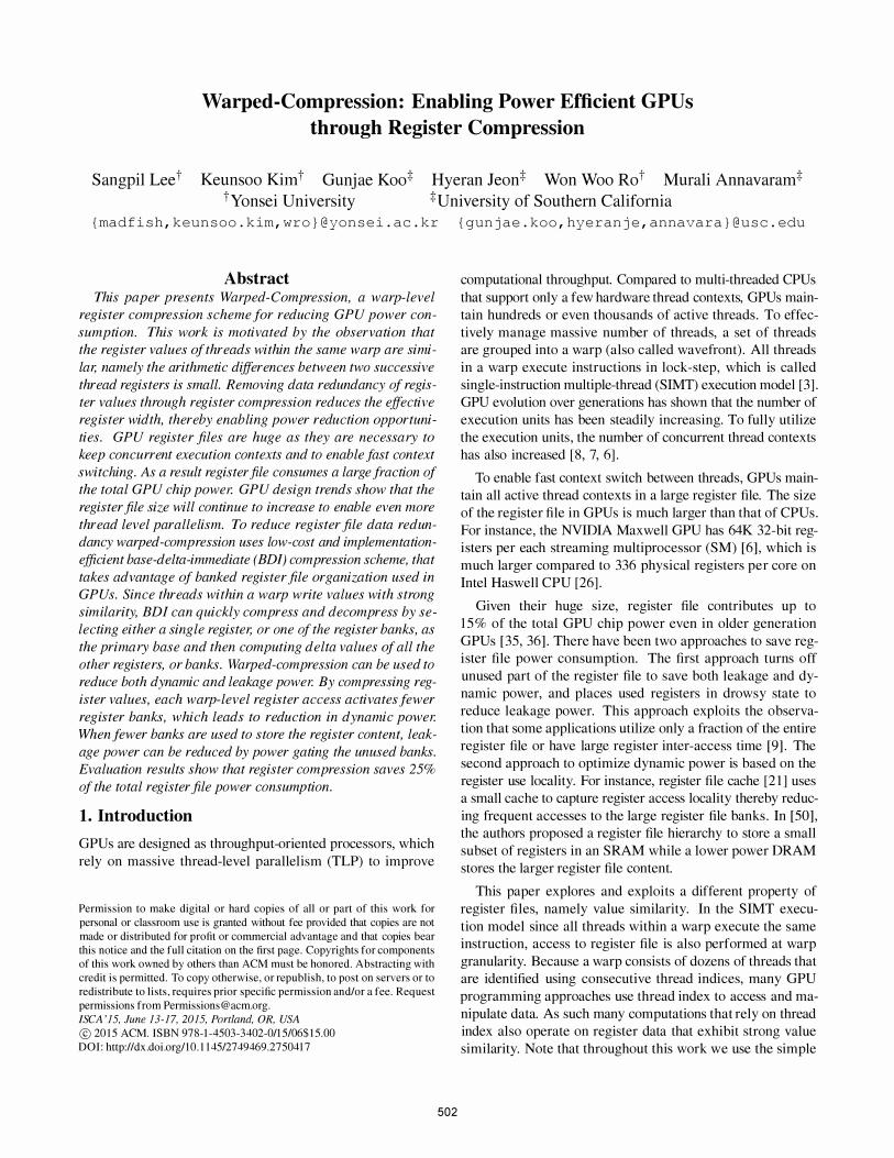
To provide large bandwidth without unduly increasing com
plexity, GPU register file is constructed with multiple SRAM
banks as shown in Figure 1 . The baseline register file design
has all the components shown in the figure except for the two
highlighted boxes, named compressor unit and decompressor
unit. The two new boxes will be described later when we
present our modified register file design. For the baseline reg
ister design, we assume a 1 28 KB register file per each SM
made up of 32 banks (4 KB registers per bank) . Each bank
has one read and one write port, and each entry in a register
bank is 1 28-bit wide, and there are 256 entries per bank. In
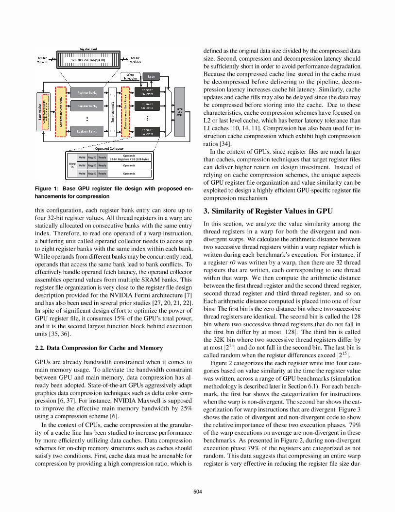
Operands 32-bit Registers X 32 (12S-byte) Valid Reg 10 Ready
��p Valid Reg 10 Ready Operands
Valid Reg 10 Ready Operands
Figure 1 : Base G PU register file d esign with proposed en
h ancements for compression
this configuration, each register bank entry can store up to
four 32-bit register values. All thread registers in a warp are
static ally allocated on consecutive banks with the same entry
index. Therefore, to read one operand of a warp instruction,
a buffering unit called operand collector needs to access up
to eight register banks with the same index within each bank.
While operands from different banks may be concurrently read,
operands that access the same bank lead to bank conflicts . To
effectively handle operand fetch latency, the operand collector
assembles operand values from multiple SRAM banks . This
register file organization is very close to the register file design
description provided for the NVIDIA Fermi architecture [7]
and has also been used in several prior studies [27 , 20, 2 1 , 22] .
In spite of significant design effort to optimize the power of
GPU register file, it consumes 15% of the GPU's total power,
and it is the second largest function block behind execution
units [35, 36] .
2.2. Data Compression for Cache and Memory
GPUs are already bandwidth constrained when it comes to
main memory usage. To alleviate the bandwidth constraint
between GPU and main memory, data compression has al
ready been adopted. State-of-the-art GPUs aggressively adapt
graphics data compression techniques such as delta color com
pression [6, 37] . For instance, NVIDIA Maxwell is supposed
to improve the effective main memory bandwidth by 25%
using a compression scheme [6] .
In the context of CPUs, cache compression at the granular
ity of a cache line has been studied to increase performance
by more efficiently utilizing data caches. Data compression
schemes for on-chip memory structures such as caches should
satisfy two conditions. First, cache data must be amenable for
compression by providing a high compression ratio, which is
504
defined as the original data size divided by the compressed data
size. Second, compression and decompression latency should
be sufficiently short in order to avoid performance degradation.
Because the compressed cache line stored in the cache must
be decompressed before delivering to the pipeline, decom
pression latency increases cache hit latency. Similarly, cache
updates and cache fills may also be delayed since the data may
be compressed before storing into the cache. Due to these
characteristics, cache compression schemes have focused on
L2 or last level cache, which has better latency tolerance than
L1 caches [ 1 0, 14, 1 1 ] . Compression has also been used for in
struction cache compression which exhibit high compression
ratios [34] .
In the context of GPUs, since register files are much larger
than caches, compression techniques that target register files
can deliver higher return on design investment. Instead of
relying on cache compression schemes, the unique aspects
of GPU register file organization and value similarity can be
exploited to design a highly efficient GPU-specific register file
compression mechanism.
3. Similarity of Register Values in GPU
In this section, we analyze the value similarity among the
thread registers in a warp for both the divergent and non
divergent warps. We calculate the arithmetic distance between
two successive thread registers within a warp register which is
written during each benchmark's execution. For instance, if
a register rO was written by a warp, then there are 32 thread
registers that are written, each corresponding to one thread
within that warp. We then compute the arithmetic distance
between the first thread register and the second thread register,
second thread register and third thread register, and so on.
Each arithmetic distance computed is placed into one of four
bins . The first bin is the zero distance bin where two successive
thread registers are identical. The second bin is called the 128
bin where two successive thread registers that do not fall in
the first bin differ by at most 1 128 1 . The third bin is called
the 32K bin where two successive thread registers differ by
at most 12ls I and do not fall in the second bin. The last bin is
called random when the register differences exceed 12ls I. Figure 2 categorizes the each register write into four cate
gories based on value similarity at the time the register value
was written, across a range of GPU benchmarks (simulation
methodology is described later in Section 6 . 1 ) . For each bench
mark, the first bar shows the categorization for instructions
when the warp is non-divergent. The second bar shows the cat
egorization for warp instructions that are divergent. Figure 3
shows the ratio of divergent and non-divergent code to show
the relative importance of these two execution phases. 79%
of the warp executions on average are non-divergent in these
benchmarks . As presented in Figure 2, during non-divergent
execution phase 79% of the registers are categorized as not
random. This data suggests that compressing an entire warp
register is very effective in reducing the register file size dur-
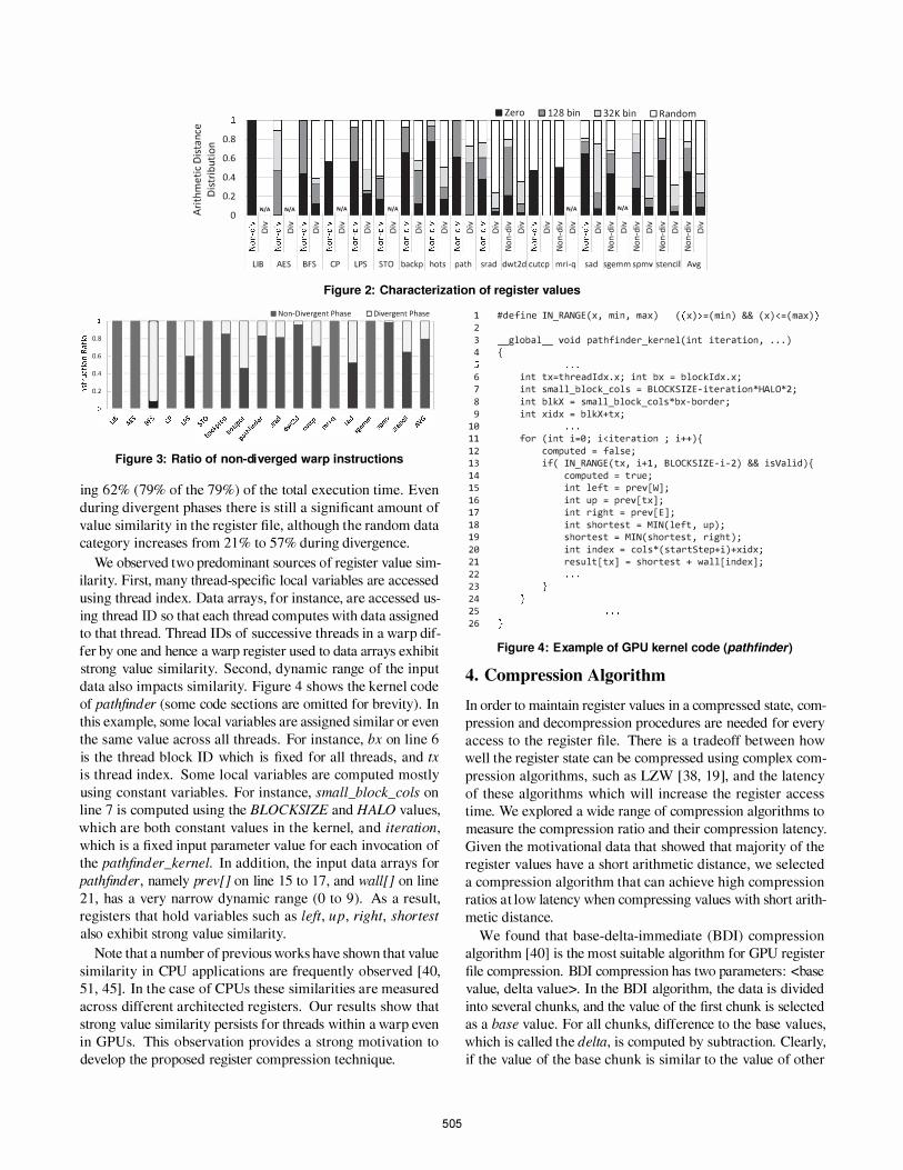
.., u c: 0.8 � :5 is :g 0.6 u.!) � '.5 0.4 E .!!! -5 Cl 0.2
� o NIA NIA
> > Ci Ci
LIB AES
NIA NIA > > > > Ci Ci Ci Ci
BFS ep LPS STD
> > > Ci Ci Ci
backp hots path
• Zero 0128 bin 0 32K bin 0 Random
> Ci
srad
> > '5 Ci C: 0 z
> > i5� c: 0 z
NIA > Ci
dwt2d cutcp mri-q
NIA
> > > > > > > > > is � i5 � i5 � is � is
C C: C C o 0 0 0 z z z z
sad sgemm spmv stencil Avg
Figure 2: Ch aracterization of register values
• Non-Divergent Phase 0 Divergent Phase
�11�lillilllilillil Figure 3: Ratio of non-diverged warp instructions
ing 62% (79% of the 79%) of the total execution time. Even
during divergent phases there is still a significant amount of
value similarity in the register file, although the random data
category increases from 2 1 % to 57% during divergence.
We observed two predominant sources of register value sim
ilarity. First, many thread-specific local variables are accessed
using thread index. Data arrays, for instance, are accessed us
ing thread ID so that each thread computes with data assigned
to that thread. Thread IDs of successive threads in a warp dif
fer by one and hence a warp register used to data arrays exhibit
strong value similarity. Second, dynamic range of the input
data also impacts similarity. Figure 4 shows the kernel code
of pathfinder (some code sections are omitted for brevity) . In
this example, some local variables are assigned similar or even
the same value across all threads . For instance, bx on line 6
is the thread block ID which is fixed for all threads, and tx is thread index. Some local variables are computed mostly
using constant variables. For instance, small_block_cols on
line 7 is computed using the BLOCKSIZE and HALO values,
which are both constant values in the kernel, and iteration, which is a fixed input parameter value for each invocation of
the pathfinder _kernel. In addition, the input data arrays for
pathfinder, namely prev[] on line 15 to 17 , and wall[] on line
2 1 , has a very narrow dynamic range (0 to 9) . As a result,
registers that hold variables such as left, up, right, shortest also exhibit strong value similarity.
Note that a number of previous works have shown that value
similarity in CPU applications are frequently observed [40,
5 1 , 45] . In the case of CPUs these similarities are measured
across different architected registers . Our results show that
strong value similarity persists for threads within a warp even
in GPUs. This observation provides a strong motivation to
develop the proposed register compression technique.
505
1 #define IN_RANGE(x, min, max) «x»=(min) && (x)<=(max»
2
3 __ global __ void pathfinder_kernel(int iteration, ... )
4 {
6 int tx=threadldx.x; int bx = blockldx.x;
7 int small_block_cols = BLOCKSIZE-iteration*HALO*2;
8 int blkX = small_block_cols*bx-border;
9 int xidx = blkX+tx;
19
11 for (int i=9; i<iteration ; i++){
12 computed = false;
13 if( IN_RANGE(tx, i+1, BLOCKSIZE-i-2) && isValid){
14
15
16
17
18 19
29
21
22
23
24
25
26
computed = true;
int left = prev[W];
int up = prev[tx];
int right = prev[E];
int shortest = MIN(left, up);
shortest = MIN(shortest, right);
int index = cols*(startStep+i)+xidx;
result[tx] = shortest + wall[index];
Figure 4: Example of G PU kernel cod e (pathfinder)
4. Compression Algorithm
In order to maintain register values in a compressed state, com
pression and decompression procedures are needed for every
access to the register file. There is a tradeoff between how
well the register state can be compressed using complex com
pression algorithms, such as LZW [38, 19 ] , and the latency
of these algorithms which will increase the register access
time. We explored a wide range of compression algorithms to
measure the compression ratio and their compression latency.
Given the motivational data that showed that maj ority of the
register values have a short arithmetic distance, we selected
a compression algorithm that can achieve high compression
ratios at low latency when compressing values with short arith
metic distance.
We found that base-delta-immediate (BDI) compression
algorithm [40] is the most suitable algorithm for GPU register
file compression. BDI compression has two parameters : <base
value, delta value>. In the BDI algorithm, the data is divided
into several chunks, and the value of the first chunk is selected
as a base value. For all chunks, difference to the base values,
which is called the delta, is computed by subtraction. Clearly,
if the value of the base chunk is similar to the value of other
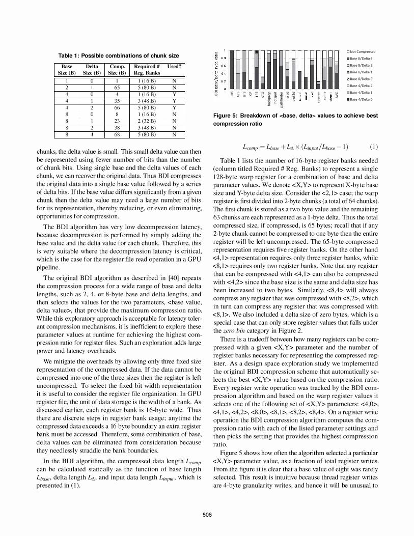
Table 1 : Possible combinations of chunk size
Base Delta Comp. Required # Used? Size (B) Size (B) Size (B) Reg. Banks
1 0 1 1 (16 E) N
2 I 65 5 (80 E) N
4 0 4 1 (16 E) Y
4 1 35 3 (48 E) Y
4 2 66 5 (80 E) Y
8 0 8 1 (16 E) N
8 1 23 2 (32 E) N
8 2 38 3 (48 E) N
8 4 68 5 (80 El N
chunks, the delta value is small. This small delta value can then
be represented using fewer number of bits than the number
of chunk bits . Using single base and the delta values of each
chunk, we can recover the original data. Thus BDI compresses
the original data into a single base value followed by a series
of delta bits . If the base value differs significantly from a given
chunk then the delta value may need a large number of bits
for its representation, thereby reducing, or even eliminating,
opportunities for compression.
The BDI algorithm has very low decompression latency,
because decompression is performed by simply adding the
base value and the delta value for each chunk. Therefore, this
is very suitable where the decompression latency is critical,
which is the case for the register file read operation in a GPU
pipeline.
The original BDI algorithm as described in [40] repeats
the compression process for a wide range of base and delta
lengths, such as 2, 4, or 8-byte base and delta lengths, and
then selects the values for the two parameters, <base value,
delta value>, that provide the maximum compression ratio.
While this exploratory approach is acceptable for latency toler
ant compression mechanisms, it is inefficient to explore these
parameter values at runtime for achieving the highest com
pression ratio for register files . Such an exploration adds large
power and latency overheads.
We mitigate the overheads by allowing only three fixed size
representation of the compressed data. If the data cannot be
compressed into one of the three sizes then the register is left
uncompressed. To select the fixed bit width representation
it is useful to consider the register file organization. In GPU
register file, the unit of data storage is the width of a bank. As
discussed earlier, each register bank is I 6-byte wide. Thus
there are discrete steps in register bank usage; any time the
compressed data exceeds a 16 byte boundary an extra register
bank must be accessed. Therefore, some combination of base,
delta values can be eliminated from consideration because
they needlessly straddle the bank boundaries .
In the BDI algorithm, the compressed data length Lcomp can be calculated static ally as the function of base length
Lbase, delta length L/',., and input data length Lil1pUIo which is
presented in ( 1 ) .
506
B '" "' � � 0- � 0 c. 8.
t "0 :;; w "' U 0- to
i � '" ]
"0 C. " "0 E � ro � B E ei'
� 'ffi '"
Cl > '"
o Not Compressed
11 Base 8/Delta 4
� Base 8/Delta 2 IZI Base 8/Delta 1 121 Base 8/Delta 0 o Base 4/Delta 2 o Base 4/Delta 1 • Base 4/Delta 0
Figure 5: Breakdown of <base, d elta> values to achieve best
compression ratio
Lcomp = Lbase + L/',. x (Lil1pu{ / Lbase - 1 ) ( 1 )
Table 1 lists the number o f I 6-byte register banks needed
(column titled Required # Reg. B anks) to represent a single
I 28-byte warp register for a combination of base and delta
parameter values . We denote <X,Y> to represent X-byte base
size and Y-byte delta size. Consider the <2, 1> case; the warp
register is first divided into 2-byte chunks (a total of 64 chunks) .
The first chunk i s stored as a two byte value and the remaining
63 chunks are each represented as a I -byte delta. Thus the total
compressed size, if compressed, is 65 bytes; recall that if any
2-byte chunk cannot be compressed to one byte then the entire
register will be left uncompressed. The 65-byte compressed
representation requires five register banks . On the other hand
<4, 1 > representation requires only three register banks, while
<8 , 1 > requires only two register banks . Note that any register
that can be compressed with <4, 1 > can also be compressed
with <4,2> since the base size is the same and delta size has
been increased to two bytes. Similarly, <8 ,4> will always
compress any register that was compressed with <8 ,2>, which
in turn can compress any register that was compressed with
<8, 1> . We also included a delta size of zero bytes, which is a
special case that can only store register values that falls under
the zero bin category in Figure 2 .
There is a tradeoff between how many registers can be com
pressed with a given <X,Y> parameter and the number of
register banks necessary for representing the compressed reg
ister. As a design space exploration study we implemented
the original BDI compression scheme that automatically se
lects the best <X,Y> value based on the compression ratio.
Every register write operation was tracked by the BDI com
pression algorithm and based on the warp register values it
selects one of the following set of <X,Y> parameters : <4,0>,
<4, 1>, <4,2>, <8 ,0>, <8, 1>, <8,2>, <8,4>. On a register write
operation the BDI compression algorithm computes the com
pression ratio with each of the listed parameter settings and
then picks the setting that provides the highest compression
ratio.
Figure 5 shows how often the algorithm selected a particular
<X,Y> parameter value, as a fraction of total register writes .
From the figure i t i s clear that a base value of eight was rarely
selected. This result is intuitive because thread register writes
are 4-byte granularity writes , and hence it will be unusual to
50% Compressed
�������� DDDDlQlQlQlQ
I. 4 Bank .1 Saved
Figure 6: Saving register banks with compression
find no similarity across two single thread registers, but to
find similarity across pairs of registers . B ased on the data
shown in this breakdown we selected <4,0>, <4, 1> , <4,2>
as the three fixed choices for compressing the data. If the
data cannot be compressed using any of the three choices
the register will be remain uncompressed. This selection is
used as our default implementation in all our results. For this
selection each warp register requires a 2-bit compression range
indicator, to indicate which of the three compression choices
were used to compress the warp register, or if the warp register
is left uncompressed. In our implementation, this vector is
stored in the bank arbiter, and it is read when a register access
is requested, in parallel to bank arbitration.
Note that in our design space exploration studies we eval
uated restricting the compression to just one choice amongst
<4,0>, <4, 1>, and <4,2>. Clearly, selecting a single compres
sion choice reduces decompression complexity but it may also
reduce compression capability. Note that <4,0> is quicker to
decompress since no delta values need to be added to the base
value, but only zero bin category in Figure 2 will benefit from
this selection. On the other hand <4, 1> improves the reach of
the BDI compression algorithm but the decompression latency
will increase. We evaluate a range of these tradeoffs in our
results sections .
5. Warped-Compression Operation
In this section, we present the detailed operation of warped
compression. Figure 1 shows the block diagram of the warped
compression with the added compression and decompression
logic highlighted. When compression is activated, the com
puted values from the execution units should be compressed
before being written to the register file. As illustrated in Figure
6, the compressed register values are split into multiple chunks,
each chunk is 1 6 bytes-wide to fit in one register bank. For
instance, if a 128-byte warp operand is compressed to 64-byte
with a compression ratio of two, the 64-byte compressed value
507
4-Byte Base r_----,r+---�+_--�r_--_r+----...,
�======�=======:7 Packing "-- J Data
Compressed Data out
Figure 7: Compressor implementation
is split into four chunks and stored to four consecutive register
banks . In this example, compression can halve the number of
register banks accessed to store, and later read that register.
As shown in Figure 1 a decompression unit is placed be
tween the execution unit and the register file. The decompres
sion of register values is performed when a register operand
of a warp instruction is read from the register file. When a
warp instruction is allocated to a collector unit, the operand
collector sends access requests for all source operands of the
instruction to the bank arbiter. In order to minimize bank con
flicts, the arbiter selects access requests that do not access the
same bank among the access requests from multiple operand
collectors . The arbiter uses the compression range indicator
vector to identify whether the register being sourced is in com
pressed state or otherwise. As described above the two-bit
compression range indicator shows the size of the compressed
register. Recall that the <4,0> BDI compression stores the
entire warp register in a single 16 byte register bank. Similarly
<4, 1 > requires three register bank reads, and <4,2> requires
five register bank reads . If the register is in uncompressed state
then all eight register banks must be read. When the arbiter
accesses a compressed warp register it needs to access only
those banks that store the compressed partial chunk of all reg
isters for a warp operand. After all the necessary banks for a
compressed operand register are read, the compressed chunks
are sent to the decompressor unit and the original 1 28-byte
register value is reconstructed.
5.1. Organization of Compressor
Figure 7 shows the detailed organization of the compressor
unit. The compression process is composed of two steps: sub
traction and bit comparison. The 128-byte warp register data is
divided into 32, 4-byte chunks. Then each chunk is subtracted
from the 4-byte base. For implementation simplicity we only
use the first chunk of original data as the base value. Sign
extension comparators compare sign bits of the subtraction
results (deltas) to determine that the subtraction results can
be represented using the delta size of either 0, 1 or 2 bytes.
Note that this compression process is activated only when the
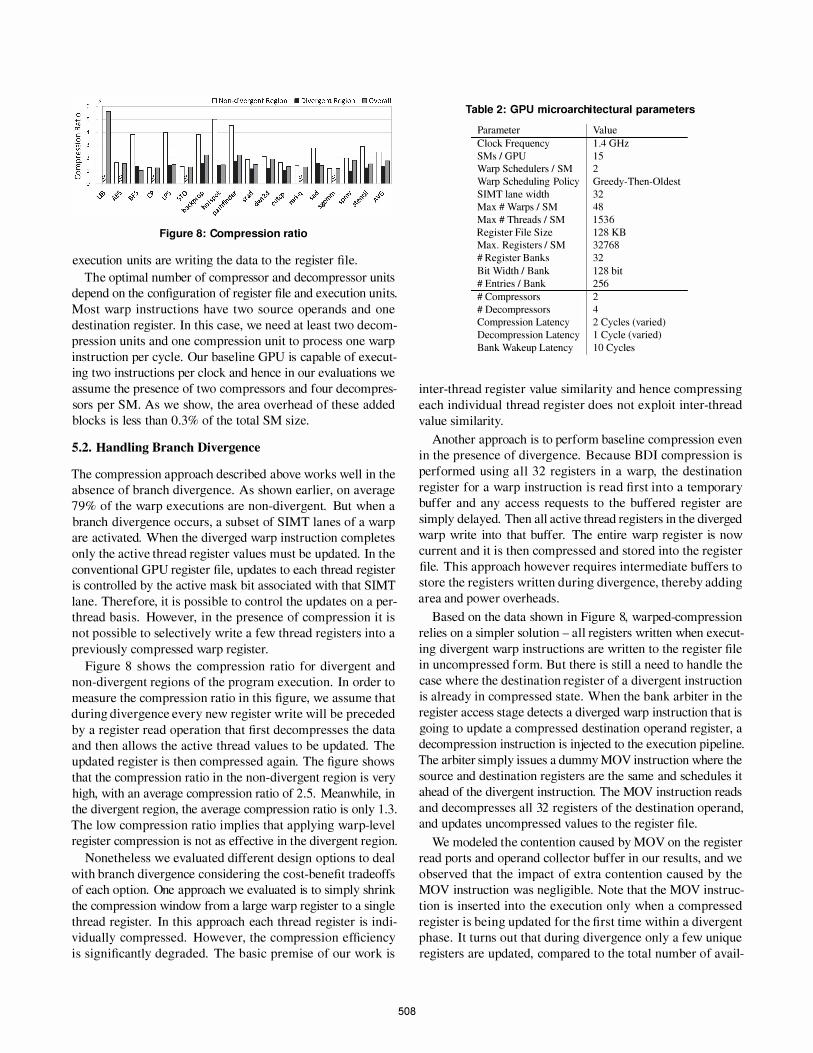
Figure 8: Compression ratio
execution units are writing the data to the register file.
The optimal number of compressor and decompressor units
depend on the configuration of register file and execution units.
Most warp instructions have two source operands and one
destination register. In this case, we need at least two decom
pression units and one compression unit to process one warp
instruction per cycle. Our baseline GPU is capable of execut
ing two instructions per clock and hence in our evaluations we
assume the presence of two compressors and four decompres
sors per SM. As we show, the area overhead of these added
blocks is less than 0 .3% of the total SM size.
5.2. Handling Branch Divergence
The compression approach described above works well in the
absence of branch divergence. As shown earlier, on average
79% of the warp executions are non-divergent. But when a
branch divergence occurs, a subset of SIMT lanes of a warp
are activated. When the diverged warp instruction completes
only the active thread register values must be updated. In the
conventional GPU register file, updates to each thread register
is controlled by the active mask bit associated with that SIMT
lane. Therefore, it is possible to control the updates on a per
thread basis . However, in the presence of compression it is
not possible to selectively write a few thread registers into a
previously compressed warp register.
Figure 8 shows the compression ratio for divergent and
non-divergent regions of the program execution. In order to
measure the compression ratio in this figure, we assume that
during divergence every new register write will be preceded
by a register read operation that first decompresses the data
and then allows the active thread values to be updated. The
updated register is then compressed again. The figure shows
that the compression ratio in the non-divergent region is very
high, with an average compression ratio of 2.5 . Meanwhile, in
the divergent region, the average compression ratio is only 1 .3 .
The low compression ratio implies that applying warp-level
register compression is not as effective in the divergent region.
Nonetheless we evaluated different design options to deal
with branch divergence considering the cost-benefit tradeoffs
of each option. One approach we evaluated is to simply shrink
the compression window from a large warp register to a single
thread register. In this approach each thread register is indi
vidually compressed. However, the compression efficiency
is significantly degraded. The basic premise of our work is
508
Table 2: G PU microarchitectural parameters
Parameter
Clock Frequency
SMs /GPU Warp Schedulers I SM
Warp Scheduling Policy
SIMT lane width
Max # Warps I SM
Max # Threads I SM
Register File Size Max. Registers I SM
# Register Banks
Bit Width I Bank
# Entries I Bank
# Compressors
# Decompressors Compression Latency
Decompression Latency
Bank Wakeup Latency
Value
1.4 GHz
15 2
Greedy-Then-Oldest
32 48
1536
128KB
32768
32
128 bit
256
2
4
2 Cycles (varied)
I Cycle (varied)
10 Cycles
inter-thread register value similarity and hence compressing
each individual thread register does not exploit inter-thread
value similarity.
Another approach is to perform baseline compression even
in the presence of divergence. Because BDI compression is
performed using all 32 registers in a warp, the destination
register for a warp instruction is read first into a temporary
buffer and any access requests to the buffered register are
simply delayed. Then all active thread registers in the diverged
warp write into that buffer. The entire warp register is now
current and it is then compressed and stored into the register
file. This approach however requires intermediate buffers to
store the registers written during divergence, thereby adding
area and power overheads .
Based on the data shown in Figure 8, warped-compression
relies on a simpler solution - all registers written when execut
ing divergent warp instructions are written to the register file
in uncompressed form. But there is still a need to handle the
case where the destination register of a divergent instruction
is already in compressed state. When the bank arbiter in the
register access stage detects a diverged warp instruction that is
going to update a compressed destination operand register, a
decompression instruction is injected to the execution pipeline.
The arbiter simply issues a dummy MOV instruction where the
source and destination registers are the same and schedules it
ahead of the divergent instruction. The MOV instruction reads
and decompresses all 32 registers of the destination operand,
and updates uncompressed values to the register file.
We modeled the contention caused by MOV on the register
read ports and operand collector buffer in our results, and we
observed that the impact of extra contention caused by the
MOV instruction was negligible. Note that the MOV instruc
tion is inserted into the execution only when a compressed
register is being updated for the first time within a divergent
phase. It turns out that during divergence only a few unique
registers are updated, compared to the total number of avail-
• RF Leakage 0 RF Dynamic IIiJ Compressor 0 Decompressor 1
> "" 0.8 Q; c
UJ 0.6 .!!!
u:: � 0.4 �
; '00 Q) 0.2 0:
0 � u � u � u � U ro 3: ro 3: ro 3: ro 3: "' "' "' "'
LIB AES BFS CP LPS STO back hot path srad dwt2d cutcp mri-q sad sgemm spmv stencil AVG
Figure 9: Register file energy consumption
Table 3: Estimated energy and power values (@45nm)
Description Value
Operating Voltage (V ) 1.0
Wire Capacitance (tF/mm) 300 Wire Energy (l2S-bit, pJ/mm) 9.6 Access energy/bank (pJ) 7 Leakage power/bank (mW) 5.S
Compression unit energy/activation (pJ) 23
Compression unit leakage power (mW) 0. 12 Decompression unit energy/activation (pJ) 21
Decompression unit leakage power (mW) O.OS
able registers . Hence, the number of MOV instructions is
only a small fraction of the total instruction count. All these
observations are quantified in detail in our results section.
5.3. Support for Reducing Leakage Energy
Apart from reducing dynamic energy by reducing bank ac
cesses, warped-compression can also reduce leakage energy.
To minimize leakage, warped-compression applies bank-level
power gating techniques for register banks that were left idle
after compression. When all the entries in a register bank are
not used, the bank is turned off to save leakage power. To
enable power gating each register bank is augmented with a
sleep transistor to control the bank power delivery, and each
register entry in a bank has a valid bit. When all the valid
bits are reset the corresponding bank is power gated and when
a single entry is needed then that bank is woken up after a
wake up delay, which was set to 1 0 cycles by default.
6. Evaluation
6.1. Methodology
We modified GPGPU-Sim [ 12] for detailed simulation of the
banked register file design, and modeled additional pipeline
stages for both the compression and decompression of the
register file. We also modeled the additional read port and
operand collector contention due to dummy MOV instructions
to handle branch divergence. Detailed GPU microarchitectral
parameters are listed in Table 2. We assume that each SM
has 4 decompressors and 2 compressors to process 2 warp
instructions per cycle from 2 warp schedulers . In order to
model overheads with bank-level power gating, we assume 10
509
� 14% � 12% � 10%
� :: � �: j 0% .1111111 ••• 11111 ••• 11111 .�
Figure 1 0: Portion of power-gated cycles for each bank
cycles are required to wake up a power-gated register bank.
We executed a wide range of benchmark applications from
Rodinia [ 1 3 ] , Parboil [5] , and GPGPU-sim [ 1 2] .
Table 3 summarizes the estimated energy and power values
for register and compression components . CACTI [ 1 ] was
used to model the access energy and leakage power of a 128-
bit wide 4 KB SRAM bank. Wire energy for data transmission
was also modeled since the warped-compression reduces the
wire movement energy, which contributes to a significant frac
tion of the total access energy per bank [29, 1 8 , 3 1 , 42] . Wire
energy was modeled using a similar methodology presented
in previous works [3 1 , 2 1 ] . For measuring the wire energy,
as presented in Table 3 , we assume the wire capacitance of
300 fF/mm and the data read from the register banks travels 1
mm [2 1 ] . We also assume 50% of wires move zeros while the
other 50% of the wires move ones.
The compression and decompression units are essentially
a collection of 32 adder/subtractor modules. The activation
energy of the adders is estimated by using the 32-bit adder
energy number from recent literature [47 ] . The other parts of
the units, such as comparators with the base value and delta
storage circuits, are modeled in RTL level and synthesized
with 45nm FreePDK library [2] . B ased on the die photo of
GF1 00, the size of an SM is estimated to be 22 mm2. The
estimated area of 2 compressors and 4 decompressors is 0 .07
mm2, which increase the area of an SM by 0 .3%.
These power and energy values were used to compute
the baseline energy savings . Since these modeled energy
values (e.g . , wire activity, activation energy of compres
sion/decompression unit) are implementation dependent, to
provide robust results we also explored a range of energy ex
penditures for the wires and the compression/decompression
logic blocks in our design space exploration results.
10%
:s .� 8%
� 6%
> 4% 0
:; E 2%
§ 0% " I I 1 •• 1.1 • I.
Figure 1 1 : Portion of d ummy MOV instructions
6.2. Energy Reduction
Figure 9 shows the total energy consumed in the register file.
For each benchmark we report two stacked bars . The first
stacked bar shows the baseline leakage and dynamic energy
consumption as a fraction of the total register file energy with
out any compression capability. The second stacked bar shows
warped-compression energy broken into four categories of en
ergy expenditure as a fraction of the total energy consumed in
the baseline without any compression. The two new categories
are the energy consumed due to compression and decompres
sion. The total energy consumption of warped-compression
is significantly less than the baseline, even after accounting
for the overhead of the compression and decompression pro
cess . Referring to the compression ratio data presented in
Figure 8, benchmarks that have high compression ratios are
the ones that benefit most from our approach. The number of
physical register banks required to store the logical registers
decrease in proportion to the compression ratio. Therefore,
warped-compression reduces the dynamic energy by reducing
bank accesses to the register file. As discussed in Section
3, the dynamic range of the input value strongly affects the
value similarity. In case of LIB, the input data is initialized
to constant values, therefore it has zero dynamic range. As a
result, most of warp registers can be perfectly compressed and
the register file energy consumption for LIB is significantly
reduced. Note that leakage energy was also reduced by the
bank-level power-gating technique, although leakage energy
savings are lower. The average dynamic and leakage energy
consumption reduced by 35% and 1 0%, respectively, which
resulted in 25% overall register file energy reduction.
Figure 1 0 shows the average ratio of power-gated cycles
for 32 register banks . We present the average values per bank
for all benchmarks. B aseline register file does not have any
bank-level power-gating opportunity because all registers are
distributed across all banks to prevent bank conflict. On the
contrary, warped-compression reduces the number of banks
for storing register data, therefore some banks do not contain
valid register data and can be power-gated safely. Recall that
a warp register is allocated to eight consecutive register banks
and as such we show the per bank gating data for four clusters
of eight consecutive banks. Since the compressed register data
is stored starting from the lowest bank index the fraction of
cycles where a bank is power gated increases as we move
towards higher bank index in each cluster.
510
o Non-divergent Region • Divergent Region
Figure 1 2: Portion of compressed registers
6.3. Impact of Branch Divergence
As discussed in our implementation section any register up
dated during branch divergence will be first uncompressed
using a dummy MOY instruction. Figure 1 1 shows the num
ber of MOY instructions executed as a fraction of the total
instruction count. MOY instructions account for less 2% of
the total instruction count. There are two reasons for the small
instruction overhead. First, only 2 1 % of the instructions on
average diverge across all benchmarks . Second, even during
the divergence only the first update to a compressed register re
sults in the MOY operation. The number of registers that were
in compressed state during divergent and non-divergent phases
of each benchmark are shown in Figure 12 . For each bench
mark we show as a fraction of the total registers allocated to
the application how many registers were in compressed state
during the non-divergent (first bar) and divergent (second bar)
phases . Note that benchmarks, such as AES, do not diverge
at all and hence the divergent region bars are marked as NI A.
Only a few benchmarks, BFS, dwt2d and spmv, show greater
than 1 0% reduction in the number of compressed registers
during divergent code. These benchmarks lose some opportu
nities for compression due to our implementation choice. For
the remaining benchmarks the number of compressed registers
stay almost the same both during divergent and non-divergent
regions. While computing the average for divergent region we
removed all those benchmarks that exhibit zero divergence.
Since we disable compression during divergence and yet it
reduces the compressed register ratio by 63% we can conclude
that only a few registers were decompressed during divergent
phase.
6.4. Impact on Execution Time
The proposed register compression may negatively impact
execution time in two ways. The first reason is the additional
pipeline stages to compress and decompress register values.
The second reason is the increased number of dummy MOY
instructions when handling branch divergence. Figure 1 3
shows the performance impact due to compression. As we
already showed earlier the number of additional dUlmny MOY
instructions is negligible. Hence, most latency increase seen
can be attributed to the increased pipeline depth. But compared
to the baseline, the average performance loss is only 0. 1 % ,
and in most cases the performance i s unchanged.
o Basel ine • Warped-Compression 1.2
Figure 1 3: I mpact on execution time
Figure 1 5: Compression ratio for various compression param
eters
6.5. Impact of Warp Scheduling
Warp scheduling does not change compression ratio but it may
impact how compressed registers from different warps may co
exist thereby changing the number of idle banks that may be
power gated. As shown in Table 2, our baseline configuration
uses Greedy-Then-Oldest (GTO) as a default warp scheduler.
To quantify the sensitivity of our results to warp scheduler,
we replaced GTO with Loose Round-Robin (LRR) scheduler
[4 1 ] . The GTO scheduling algorithm runs a warp until the
warp stalls then switches the oldest ready warp, whereas the
LRR scheduling switches warps in every scheduling cycle in
round-robin order, as long as there is a waiting ready warp.
Figure 14 shows register energy consumption of GPU using
the LRR and GTO warp scheduling algorithms normalized
to the total register power consumed without compression.
The average energy reduction with LRR is 26% which is very
similar to the energy reduction with GTO (25%).
6.6. Design Space Exploration: Compression Parameters
Till now we assumed that the basic compression engine ex
plores <4,0>, <4, 1 >, and <4,2> compression parameters and
selects the parameter with the highest compression ratio with
least number of required register bank accesses. In this sec
tion, we explore a simpler compression scheme that selects
only one of the three choices static ally. Such an implementa
tion reduces the compression and decompression latencies and
energy consumption, at the expense of missed opportunities
for compression or unnecessary delta storages . For instance,
when a register value could be compressed effectively with
<4, 1 > then using <4,2> as the only compression choice leads
to an additional byte of delta value for each 4-byte chunk. In
addition, <4,0> correspond to scalarizing input operands [33] ,
because <4,0> compression essentially captures those scenar
ios where all 32 thread register values are identical. Thus an
511
D Greedy-Then-Oldest • loose Round-Robin
Figure 1 4: Energy reduction: GTO and LRR warp sched ulers
1.2 � 1 UJ 0.8 . � 0.6 � 0.4 � 0.2
0 <4, 0> only 0 <4, 1> only 0 <4, 2> only . Warped-Co m p ression
Figure 1 6: Energy consumption for various compression pa
rameters
implementation that selects only <4,0> allows us to quantify
the benefits of our proposed scheme compared to the scalariza
tion approach [33] in terms of compression ratio and energy
benefits .
Figure 1 5 shows the compression ratios seen when using
only one set of compression parameters . The baseline is la
be led as Warped-Compression in the figure. The compression
ratio of <4,0> is about 30% less than the warped-compression
scheme which selects one of the three choices dynamically.
Note that while <4, 1 > can compress every register that was
compressed with <4,0> it does not necessarily mean <4, 1 >
has better compression ratio since an extra byte i s stored for
each chunk in this case. Thus it is possible that selecting just
<4, 1 > has worse compression ratio than selecting just <4,0>,
as was the case in a few benchmarks . Since the compression
ratio of <4,0> is about 30% worse than warped-compression,
as shown in Figure 16 the dynamic energy consumed by <4,0>
is worse than the dynamic energy consumed using the warped
compression scheme.
6.7. Design Space Exploration: Access Energy Variations
In this section, we show the impact of increasing the com
pression and decompression unit activation energy by 1 .5 x ,
2 x and 2 .5 x the baseline energy data shown in Table 3 . Fig
ure 17 shows the register file energy consumption using three
different compression and decompression unit activation en
ergy values . The bar labeled 1 .5 x shows the total register file
energy consumed when compression and decompression both
take 1 . 5 x the unit activation energy normalized to a design
that does not use compression. Similarly 2 .0 x , 2 .5 x show
the case when compression and decompression unit activation
energies were increased by 2 .0 x and 2 .5 x over the baseline
data shown in Table 3. For this data the register file access
energy was kept same as the data shown in Table 3 . Thus this
data is a pessimistic view of the compression approach where
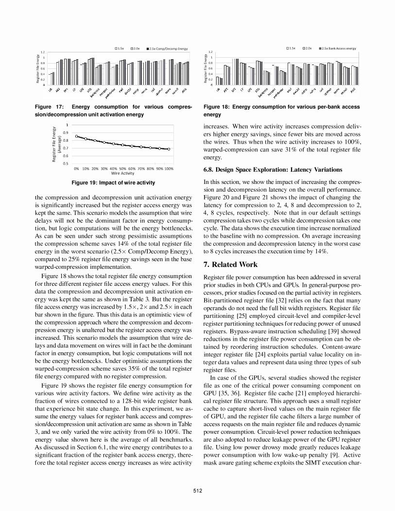
1.2 > � 1
L&.J 0.8 . II 0.6 � 0.4 & 0.2
o l.Sx 0 2.0x • 2.Sx Cam p/Deca m p Energy
Figure 1 7: Energy consumption for various compres-
sion/d ecompression unit activation energy
� QJ 0.9 c _
W QJ � � 0.8
u::: � � � 0.7
1;: -'00 0 . 6 QJ
'" 0 . 5
0% 10% 20% 30% 4 0 % 50% 6 0 % 7 0 % 8 0 % 90% 100%
Wire Activity
Figure 1 9: I mpact of wire activity
the compression and decompression unit activation energy
is significantly increased but the register access energy was
kept the same. This scenario models the assumption that wire
delays will not be the dominant factor in energy consump
tion, but logic computations will be the energy bottlenecks .
As can be seen under such strong pessimistic assumptions
the compression scheme saves 14% of the total register file
energy in the worst scenario (2.5 x Comp/Decomp Energy),
compared to 25% register file energy savings seen in the base
warped-compression implementation.
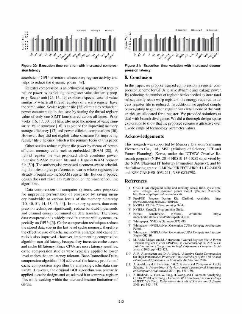
Figure 1 8 shows the total register file energy consumption
for three different register file access energy values . For this
data the compression and decompression unit activation en
ergy was kept the same as shown in Table 3. But the register
file access energy was increased by 1 .5 x , 2 x and 2 .5 x in each
bar shown in the figure. Thus this data is an optimistic view of
the compression approach where the compression and decom
pression energy is unaltered but the register access energy was
increased. This scenario models the assumption that wire de
lays and data movement on wires will in fact be the dominant
factor in energy consumption, but logic computations will not
be the energy bottlenecks . Under optimistic assumptions the
warped-compression scheme saves 35% of the total register
file energy compared with no register compression.
Figure 19 shows the register file energy consumption for
various wire activity factors . We define wire activity as the
fraction of wires connected to a 1 28-bit wide register bank
that experience bit state change. In this experiment, we as
sume the energy values for register bank access and compres
sion/decompression unit activation are same as shown in Table
3 , and we only varied the wire activity from 0% to 100%. The
energy value shown here is the average of all benchmarks.
As discussed in Section 6 . 1 , the wire energy contributes to a
significant fraction of the register bank access energy, there
fore the total register access energy increases as wire activity
512
1.2 > � 1
L&.J 0.8 . II 0.6 � 0.4 & 0.2
o l.Sx 0 2.0x • 2.Sx Bank Access energy
Figure 1 8: Energy consumption for various per-bank access
energy
increases . When wire activity increases compression deliv
ers higher energy savings, since fewer bits are moved across
the wires. Thus when the wire activity increases to 1 00%,
warped-compression can save 31 % of the total register file
energy.
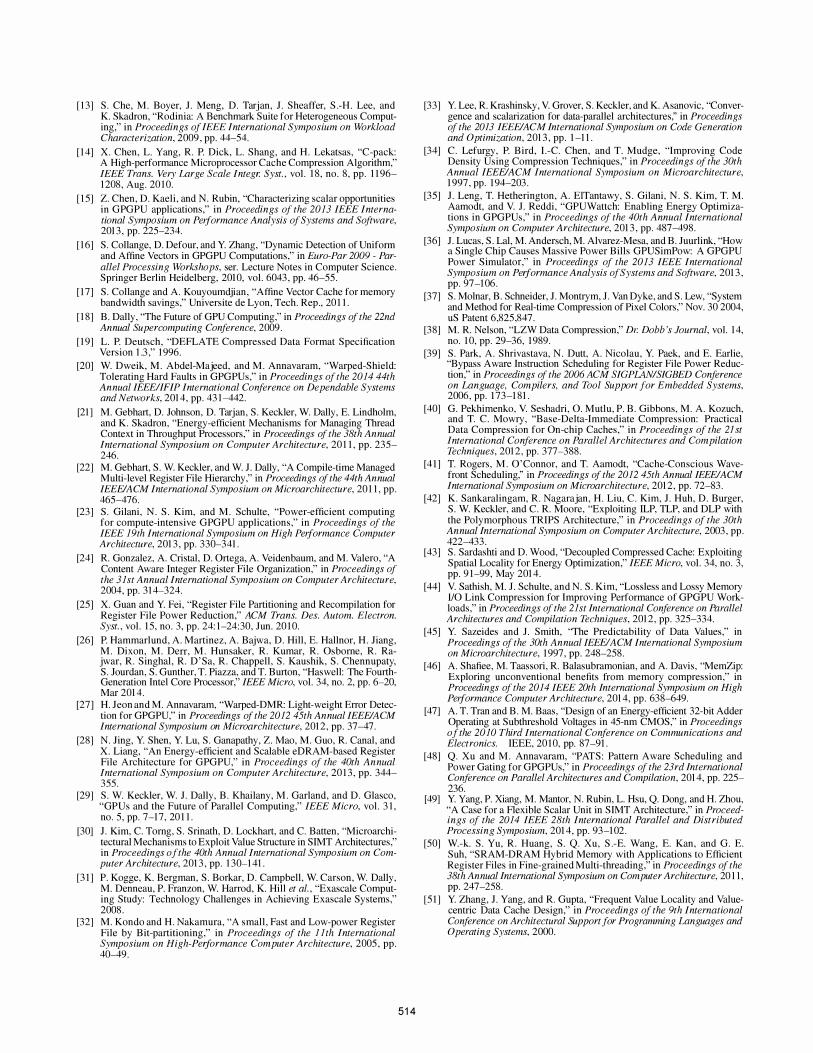
6.8. Design Space Exploration: Latency Variations
In this section, we show the impact of increasing the compres
sion and decompression latency on the overall performance.
Figure 20 and Figure 21 shows the impact of changing the
latency for compression to 2, 4, 8 and decompression to 2,
4, 8 cycles, respectively. Note that in our default settings
compression takes two cycles while decompression takes one
cycle. The data shows the execution time increase normalized
to the baseline with no compression. On average increasing
the compression and decompression latency in the worst case
to 8 cycles increases the execution time by 14%.
7. Related Work
Register file power consumption has been addressed in several
prior studies in both CPUs and GPUs. In general-purpose pro
cessors , prior studies focused on the partial activity in registers.
Bit-partitioned register file [32] relies on the fact that many
operands do not need the full bit width registers. Register file
partitioning [25] employed circuit-level and compiler-level
register partitioning techniques for reducing power of unused
registers. Bypass-aware instruction scheduling [39] showed
reductions in the register file power consumption can be ob
tained by reordering instruction schedules . Content-aware
integer register file [24] exploits partial value locality on in
teger data values and represent data using three types of sub
register files.
In case of the GPUs, several studies showed the register
file as one of the critical power consuming component on
GPU [35, 36] . Register file cache [2 1 ] employed hierarchi
cal register file structure. This approach uses a small register
cache to capture short-lived values on the main register file
of GPU, and the register file cache filters a large number of
access requests on the main register file and reduces dynamic
power consumption. Circuit-level power reduction techniques
are also adopted to reduce leakage power of the GPU register
file. Using low power drowsy mode greatly reduces leakage
power consumption with low wake-up penalty [9] . Active
mask aware gating scheme exploits the SIMT execution char-
1.6 D Comp 2 D Comp 4 . Camp 8
Figure 20: Execution time variation with increased compres
sion latency
acteristic of GPU to remove unnecessary register activity and
helps to reduce the dynamic power [48] .
Register compression is an orthogonal approach that tries to
reduce power by exploiting the register value similarity prop
erty. Scalar unit [23, 15 , 49] exploits a special case of value
similarity where all thread registers of a warp register have
the same value. Scalar register file [23] eliminates redundant
power consumption in that case by storing the thread register
value of only one SIMT lane shared across all lanes. Prior
works [ 1 6, 17 , 30, 33] have also used the notion of value simi
larity. Value structure [ 1 6] is exploited for improving memory
storage efficiency [ 17] and power efficient computations [30] .
However, they did not exploit value structure for improving
register file efficiency, which is the primary focus of this paper.
Other studies reduce register file power by means of power
efficient memory cells such as embedded DRAM [28] . A
hybrid register file was proposed which combines power
intensive SRAM register file and a large eDRAM register
file [50] . The authors also proposed a context-aware schedul
ing that tries to give preference to warps whose registers are
already brought into the SRAM register file. But our proposed
design does not place any restriction on the warp scheduling
algorithms.
Data compression on computer systems were proposed
for improving performance of processor by saving mem
ory bandwidth at various levels of the memory hierarchy
[ 1 0, 40, 5 1 , 14, 43, 46, 44] . In memory systems, data com
pression techniques significantly reduce bandwidth demands
and channel energy consumed on data transfer. Therefore,
data compression is widely used in commercial systems, es
pecially on GPUs [6] . Cache compression techniques reduce
the stored data size in the last level cache memory, therefore
the effective size of cache memory is enlarged and cache hit
ratio is also improved. However, implementing compression
algorithm can add latency because they increases cache access
and cache fill latency. Since CPUs are more latency sensitive,
cache compression studies were typically applied to lower
level caches that are latency tolerant. Base-Immediate-Delta
compression algorithm [40] addressed the latency problem of
cache compression algorithm by analyzing cache data sim
ilarity. However, the original BDI algorithm was primarily
applied to cache designs and we adapted it to compress register
files while working within the microarchitecture limitations of
GPUs.
5 1 3
1.6 o Decomp 2 0 Decamp 4 • Decomp 8
Figure 21 : Execution time variation with increased d ecom
pression latency
8. Conclusion
In this paper, we propose warped-compression, a register com
pression scheme for GPUs to save dynamic and leakage power.
By reducing the number of register banks needed to store (and
subsequently read) warp registers , the energy required to ac
cess register file is reduced. In addition, we applied simple
power-gating to gate each register bank when none of the bank
entries are allocated for a register. We provided solutions to
deal with branch divergence. We did a thorough design space
exploration to show that the proposed scheme is attractive over
a wide range of technology parameter values .
Acknowledgements
This research was supported by Memory Division, Samsung
Electronics Co . , Ltd. , MSP (Ministry of Science, ICT and
Future Planning) , Korea, under the ICT/SW Creative Re
search program (NIPA-20 14-H05 1 O- 14- 1 028) supervised by
the NIPA (National IT Industry Promotion Agency), and by
the following grants : DARPA-PERFECT-HROO I I - 1 2-2-0020
and NSF-CAREER-09542 1 1 , NSF-0834798.
References
[l] CACTI: An integrated cache and memory access time, cycle time, area, leakage, and dynamic power model. [Online]. Available: http://www.hpl.hp.comlresearch/cacti/
[2] FreePDK Process Design Kit. [Online]. Available: http: //www.eda.ncsu.edu/wikilFreePDK
[3] NV IDlA, CUDA C Programming Guide.
[4] NV IDIA, OpenCL Programming Guide.
[5] Parboil Benchmarks. [Online]. Available: http: // impact.crhc.illinois.edu/ParboiIlparboil.aspx
[6] Whitepaper: NVlDIA GeForce GTX 980.
[7] Whitepaper: NVlDlAs Next Generation CUDA Compute Architecture: Fermi.
[8] Whitepaper: NVlDIAs Next Generation CUDA Compute Architecture: KeplerGKllO.
[9] M. Abdel-Majeed and M. Annavaram, "Warped Register File: A Power Efficient Register File for GPGPUs," in Proceedings of the 2013 IEEE 1 9th International Symposium on High Peiformance Computer Architecture, 2013, pp. 412-423.
[ 10] A. R. Alameldeen and D. A. Wood, "Adaptive Cache Compression for High-Performance Processors," in Proceedings of the 31st Annual International Symposium on Computer Architecture, 2004.
[11] A. Arelakis and P. Stenstrom, "SC2: A Statistical Compression Cache Scheme," in Proceedings of the 41st Annual International Symposium on Computer Architecuture, 2014, pp. 145-156.
[ 12] A. Bakhoda, G. Yuan, W. Fung, H. Wong, and T. Aamodt, "Analyzing CUDA Workloads Using a Detailed GPU Simulator," in Proceedings of IEEE Int' l Symp. Peiformance Analysis of Systems and Software, 2009, pp. 163-174.
[ 13] S. Che, M. Boyer, 1. Meng, D. Tarjan, J. Sheaffer, S.-H. Lee, and K. Skadron, "Rodinia: A Benchmark Suite for Heterogeneous Computing," in Proceedings of IEEE International Symposium on Workload Characterization, 2009, pp. 44-54.
[l4] X. Chen, L. Yang, R. P. Dick, L. Shang, and H. Lekatsas, "C-pack: A High-performance Microprocessor Cache Compression Algorithm," IEEE Trans. Very Large Scale Integr. Syst. , vol. 18, no. 8, pp. 1196-1208, Aug. 2010.
[ 15] Z. Chen, D. Kaeli, and N. Rubin, "Characterizing scalar opportunities in GPGPU applications," in Proceedings of the 2013 IEEE International Symposium on Peiformance Analysis of Systems and Software, 2013, pp. 225-234.
[l6] S. Collange, D. Defour, and Y. Zhang, "Dynamic Detection of Uniform and Affine Vectors in GPGPU Computations," in Euro-Par 2009 - Parallel Processing Workshops, ser. Lecture Notes in Computer Science. Springer Berlin Heidelberg, 2010, vol. 6043, pp. 46-55.
[l7] S. Collange and A. Kouyoumdjian, "Affine Vector Cache for memory bandwidth savings," Universite de Lyon, Tech. Rep., 2011.
[l8] B. Dally, "The Future of GPU Computing," in Proceedings of the 22nd Annual Supercomp uting Conference, 2009.
[l9] L. P. Deutsch, "DEFLATE Compressed Data Format Specification Version 1.3," 1996.
[20] W Dweik, M. Abdel-Majeed, and M. Annavaram, "Warped-Shield: Tolerating Hard Faults in GPGPUs," in Proceedings of the 2014 44th AnnuaI IEEE/IFlP International Conference on Dependable Systems and Networks, 2014, pp. 431-442.
[21] M. Gebhart, D. 10hnson, D. Tarjan, S. KeckJer, W Dally, E. Lindholm, and K. Skadron, "Energy-efficient Mechanisms for Managing Thread Context in Throughput Processors," in Proceedings of the 38th Annual International Symposium on Computer Architecture, 2011, pp. 235-246.
[22] M. Gebhart, S. W. Keckler, and W. 1. Dally, "A Compile-time Managed Multi-level Register File Hierarchy," in Proceedings of the 44th Annual IEEE/ACM International Symposium on Microarchitecture, 2011, pp. 465-476.
[23] S. Gilani, N. S. Kim, and M. Schulte, "Power-efficient computing for compute-intensive GPGPU applications," in Proceedings of the IEEE 19th International Symposium on High Peiformance Computer Architecture, 2013, pp. 330-341.
[24] R. Gonzalez, A. Cristal, D. Ortega, A. Veidenbaum, and M. Valero, "A Content Aware Integer Register File Organization," in Proceedings of the 31st Annual International Symposium on Computer Architecture, 2004, pp. 314-324.
[25] X. Guan and Y. Fei, "Register File Partitioning and Recompilation for Register File Power Reduction," ACM Trans. Des. Autom. Electron. Syst. , vol. 15, no. 3, pp. 24: 1-24:30, Jun. 2010.
[26] P. Hammarlund, A. Martinez, A. Bajwa, D. Hill, E. Hallnor, H. Jiang, M. Dixon, M. Derr, M. Hunsaker, R. Kumar, R. Osborne, R. Rajwar, R. Singhal, R. D'Sa, R. Chappell, S. Kaushik, S. Chennupaty, S. 10urdan, S. Gunther, T. Piazza, and T. Burton, "Haswell: The FourthGeneration Intel Core Processor," IEEE Micro, vol. 34, no. 2, pp. 6-20, Mar 2014.
[27] H. Jeon and M. Annavaram, "Warped-DMR: Light-weight Error Detection for GPGPU," in Proceedings of the 2012 45th AnnuaI IEEE/ACM International Symposium on Microarchitecture, 2012, pp. 37-47.
[28] N. Jing, Y. Shen, Y. Lu, S. Ganapathy, Z. Mao, M. Guo, R. Canal, and X. Liang, "An Energy-efficient and Scalable eDRAM-based Register File Architecture for GPGPU," in Proceedings of the 40th Annual International Symposium on Computer Architecture, 2013, pp. 344-355.
[29] S. W Keckler, W J. Dally, B. Khailany, M. Garland, and D. Glasco, "GPUs and the Future of Parallel Computing," IEEE Micro, vol. 31, no. 5, pp. 7-17, 2011.
[30] J. Kim, C. Torng, S. Srinath, D. Lockhart, and C. Batten, "Microarchitectural Mechanisms to Exploit Value Structure in SIMT Architectures," in Proceedings of the 40th Annual International Symposium on Computer Architecture, 2013, pp. 130-141.
[31] P. Kogge, K. Bergman, S. Borkar, D. Campbell, W Carson, W. Dally, M. Denneau, P. Franzon, W. Harrod, K. Hill et aI. , "Exascale Computing Study: Technology Challenges in Achieving Exascale Systems," 2008.
[32] M. Kondo and H. Nakamura, "A small, Fast and Low-power Register File by Bit-partitioning," in Proceedings of the 1 1 th International Symposium on High-Peiformance Computer Architecture, 2005, pp. 40-49.
514
[33] Y. Lee, R. Krashinsky, V. Grover, S. Keckler, and K. Asanovic, "Convergence and scalarization for data-parallel architectures;' in Proceedings of the 2013 IEEE/A CM International Symposium on Code Generation and Optimization, 2013, pp. 1-11.
[34] C. Lefurgy, P. Bird, I.-C. Chen, and T. Mudge, "Improving Code Density Using Compression Techniques," in Proceedings of the 30th Annual IEEE/ACM International Symposium on Microarchitecture, 1997, pp. 194-203.
[35] J. Leng, T. Hetherington, A. EITantawy, S. Gilani, N. S. Kim, T. M. Aamodt, and V. J. Reddi, "GPUWattch: Enabling Energy Optimizations in GPGPUs," in Proceedings of the 40th Annual International Symposium on Computer Architecture, 2013, pp. 487-498.
[36] 1. Lucas, S. Lal, M. Andersch, M. Alvarez-Mesa, and B. luurlink, "How a Single Chip Causes Massive Power Bills GPUSimPow: A GPGPU Power Simulator," in Proceedings of the 2013 IEEE International Symposium on Peiformance Analysis of Systems and Software, 2013, pp. 97-106.
[37] S. Molnar, B. Schneider, J. Montrym, J. Van Dyke, and S. Lew, "System and Method for Real-time Compression of Pixel Colors," Nov. 30 2004, uS Patent 6,825,847.
[38] M. R. Nelson, "LZW Data Compression," Dr. Dobb 's Journal, vo!. 14, no. 10, pp. 29-36, 1989.
[39] S. Park, A. Shrivastava, N. Dutt, A. Nicolau, Y. Paek, and E. Earlie, "Bypass Aware Instruction Scheduling for Register File Power Reduction," in Proceedings of the 2006 ACM SIGPLAN/SIGBED Conference on Language, Compilers, and Tool Support for Embedded Systems, 2006, pp. 173-181.
[40] G. Pekhimenko, V. Seshadri, O. Mutlu, P. B. Gibbons, M. A. Kozuch, and T. C. Mowry, "Base-Delta-Immediate Compression: Practical Data Compression for On-chip Caches," in Proceedings of the 21 st International Conference on Parallel Architectures and Compilation Techniques, 2012, pp. 377-388.
[41] T. Rogers, M. O'Connor, and T. Aamodt, "Cache-Conscious Wavefront Scheduling;' in Proceedings of the 2012 45th Annual IEEE/A CM International Symposium on Microarchitecture, 2012, pp. 72-83.
[42] K. Sankaralingam, R. Nagarajan, H. Liu, C. Kim, J. Huh, D. Burger, S. W Keckler, and C. R. Moore, "Exploiting ILP, TLP, and DLP with the Polymorphous TRIPS Architecture," in Proceedings of the 30th Annual International Symposium on Computer Architecture, 2003, pp. 422-433.
[43] S. Sardashti and D. Wood, "Decoupled Compressed Cache: Exploiting Spatial Locality for Energy Optimization," IEEE Micro, vol. 34, no. 3, pp. 91-99, May 2014.
[44] V. Sathish, M. J. Schulte, and N. S. Kim, "Lossless and Lossy Memory VO Link Compression for Improving Performance of GPGPU Workloads," in Proceedings of the 21st International Conference on Parallel Architectures and Compilation Techniques, 2012, pp. 325-334.
[45] Y. Sazeides and J. Smith, "The Predictability of Data Values," in Proceedings of the 30th Annual IEEElACM International Symposium on Microarchitecture, 1997, pp. 248-258.
[46] A. Shafiee, M. Taassori, R. Balasubramonian, and A. Davis, "MemZip: Exploring unconventional benefits from memory compression," in Proceedings of the 2014 IEEE 20th International Symposium on High Peiformance Computer Architecture, 2014, pp. 638-649.
[47] A. T. Tran and B. M. Baas, "Design of an Energy-efficient 32-bit Adder Operating at Subthreshold Voltages in 45-nm CMOS," in Proceedings of the 2010 Third International Conference on Communications and Electronics. IEEE, 2010, pp. 87-91.
[48] Q. XU and M. Annavaram, "PATS: Pattern Aware Scheduling and Power Gating for GPGPUs," in Proceedings of the 23rd International Conference on Parallel Architectures and Compilation, 2014, pp. 225-236.
[49] Y. Yang, P. Xiang, M. Mantor, N. Rubin, L. Hsu, Q. Dong, and H. Zhou, "A Case for a Flexible Scalar Unit in SIMT Architecture," in Proceedings of the 2014 IEEE 28th International Parallel and Distributed Processing Symposium, 2014, pp. 93-102.
[50] W-k. S. Yu, R. Huang, S. Q. Xu, S.-E. Wang, E. Kan, and G. E. Suh, "SRAM-DRAM Hybrid Memory with Applications to Efficient Register Files in Fine-grained Multi-threading," in Proceedings of the 38th Annual International Symposium on Computer Architecture, 20 11, pp. 247-258.
[51] Y. Zhang, J. Yang, and R. Gupta, "Frequent Value Locality and Valuecentric Data Cache Design," in Proceedings of the 9th International Conference on Architectural Support for Programming Languages and Operating Systems, 2000.
Recommended