University of Nairobi
A Phase Detector for Phase Perturbation
Demodulation in a LASER Signal
Project Index: PRJ067
by
Brian Wekesa Simiyu
Reg. No: F17/1412/2011
SUPERVISOR: Dr. Ing. Wilfred Mwema
EXAMINER: Prof. Elijah Mwangi
Project Report Submitted in Partial Fulfilment of the Requirement for the Award of the
Degree of Bachelor of Science in Electrical and Electronic Engineering of the University of
Nairobi
May 16th, 2016
Department of Electrical and Information Engineering
i
Declaration of Originality
College: Architecture and Engineering
Faculty/ School/ Institute: Engineering
Department: Electrical and Information Engineering
Course: Bachelor of Science in Electrical and Electronic Engineering
Registration Number: F17/1412/2011
Name of Student: Brian Wekesa Simiyu
Title of Work: A phase detector for phase perturbation demodulation in a LASER
signal
1. I understand what plagiarism is and I am aware of the University policy in this regard.
2. I declare that this final year project report is my original work and has not been
submitted elsewhere for examination, award of a degree or publication. Where other
people’s work or my own work has been used, this has properly been acknowledged
and referenced in accordance with the University of Nairobi’s requirements.
3. I have not sought or used the services of any professional agencies to produce this work.
4. I have not allowed, and shall not allow anyone to copy my work with the intention of
passing it off as his/her own work.
5. I understand that any false claim in respect of this work shall result in disciplinary action,
in accordance with University anti-plagiarism policy
Signature Date

ii
Dedicated to
my mum

iii
Acknowledgements This project would not have been possible without the help of many wonderfully helpful
people, to whom I am deeply indebted. It was an honour to work under the supervision of Dr.
Ing. Wilfred Mwema. He introduced me to the project. His refreshing and informed advice
helped me through the project and the writing of this report. Thank you.
I would also like to thank the Electrical Engineering Department at the University of Nairobi for
facilitating my project, especially Mr. Rotich of the Telecommunications Laboratory for ensuring
I had most of what I needed for the project. To the Electronics Laboratory team, I am more than
grateful for providing space and equipment for my project implementation and testing.
Words cannot how grateful I am to my family. Because of their love and encouragement I made
it this far. Heartfelt thanks to my mother, brothers and sister for their constant encouragement
and motivation over time that has made me who I am.
iv
Contents
Declaration of Originality .............................................................................................................................. i
Dedication...................................................................................................... Error! Bookmark not defined.
Acknowledgements ..................................................................................................................................... iii
Contents ....................................................................................................................................................... iv
List of Figures ............................................................................................................................................... vi
List of Tables ............................................................................................................................................... vii
List of Symbols ........................................................................................................................................... viii
List of Abbreviations ................................................................................................................................... ix
ABSTRACT ..................................................................................................................................................... x
1.0 INTRODUCTION ................................................................................................................................ 1
2.0 BACKROUND AND THEORY .............................................................................................................. 2
2.1 Interference .................................................................................................................................. 2
2.2 Doppler Effect ............................................................................................................................... 2
2.3 Interferometry .............................................................................................................................. 3
2.3.1 External Interferometry: The Michelson Interferometer ................................................... 4
2.3.2 Self-Mixing Interferometer .................................................................................................. 4
2.4 LASER Diodes ................................................................................................................................ 8
2.5 Photodiodes .................................................................................................................................. 9
3.0 METHODOLOGY .............................................................................................................................. 11
3.1 Choice of Implementation method ........................................................................................... 11
3.2 Choice of the LASER diode ......................................................................................................... 13
3.3 Design of the LASER Diode Driver .............................................................................................. 13
3.4 Design of the Trans Impedance Amplifier ................................................................................. 16
3.5 Design of the Low Pass Filter ..................................................................................................... 18
4.0 IMPLEMENTATION AND TESTING .................................................................................................. 24
4.1. Testing of the Complete Detector ............................................................................................. 25
4.2. Testing of the LASER driver ........................................................................................................ 27
4.3. Testing of the Transimpedance Amplifier ................................................................................. 29
4.4. Testing of the Lowpass Filter ..................................................................................................... 30
v
5.0 DISCUSSION .................................................................................................................................... 32
6.0 CONCLUSION .................................................................................................................................. 33
7.0 RECOMMENDATIONS ..................................................................................................................... 34
8.0 REFERENCES .................................................................................................................................... 35
vi
List of Figures Figure 1: Illustration of Doppler Shifting by Back Scattering………………………………………………..……3
Figure 1: Set up of the Michelson Interferometer……………………………………………………….………………4
Figure 2: Basic Scheme of a Self-Mixing Interferometer………………………………………….………………….5
Figure 3: Self-mixing output for different feedback regimes with respect to the target
vibration……………………………………………………………………………………………………………………………..….….8
Figure 4: Photodiode Equivalent Circuit…………………………………………………………………………….……..9
Figure 5: Block Diagram of the Phase Detector…………………………………………………………………..……12
Figure 6: Circuit of the Laser Diode Current Source (Driver)… …………………………………………..….….14
Figure 7: Circuit of the Transimpedance Amplifier………………….…………………………………………….….16
Figure 8: Spectral Response of Various Silicon Photodiodes…………….……………………………………....19
Figure 9: Second order Sallen-Key topology………………………………….………………………………………….20
Figure 10: Circuit of the Low Pass Filter……………………………………………………………………………………22
Figure 11: Simulated filter response………………………………………….…………………………………………….23
Figure 12: Schematic capture of the complete detector……………………………………………………………24
Figure 13: Board Layout of the Phase detector…………………………………………………………………………25
Figure 14: Illustration of the fringe counting method………………………………………………………………25
Figure 15: Phase detector testing set up………………………………………..…………………………………………27
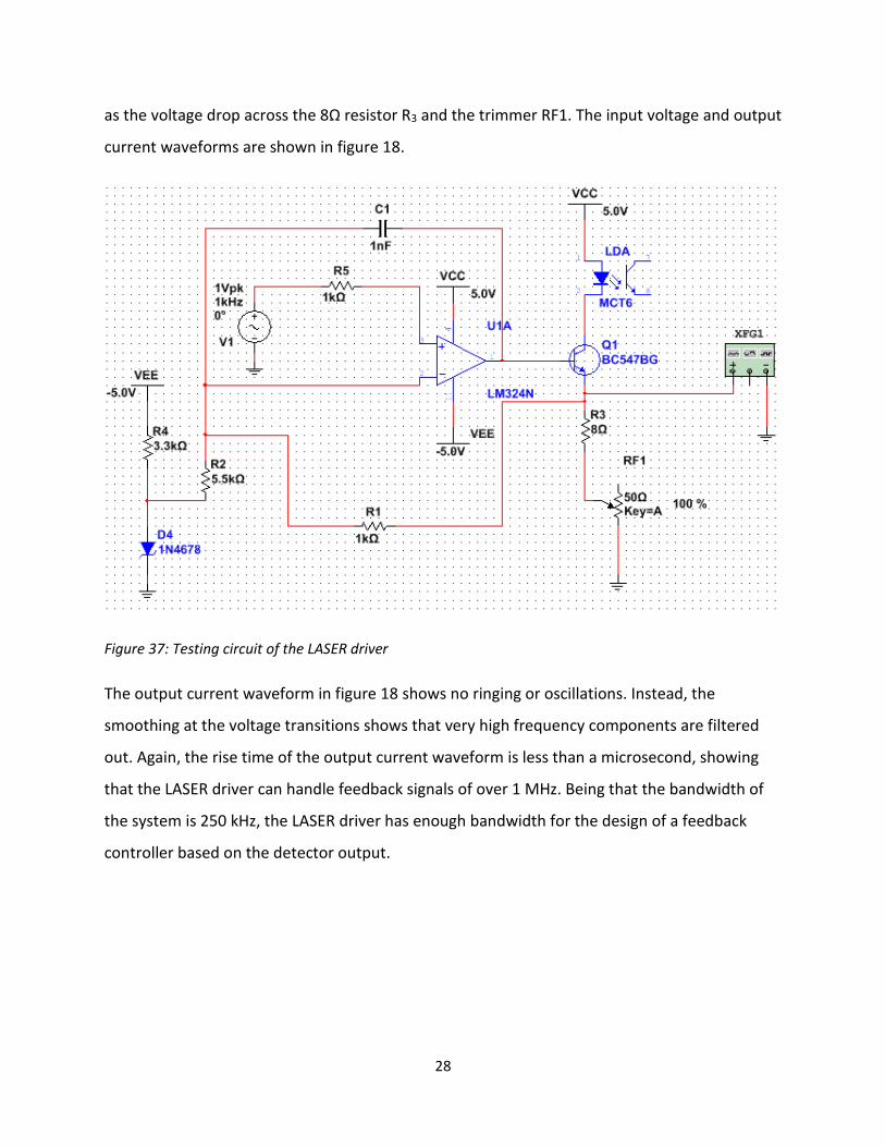
Figure 16: Testing circuit of the LASER driver……………………………………………………………………………28
Figure 17: Input Voltage and Output Current Waveforms……………..…………………………………………29
Figure 18: Multisim simulation set up for the transimpedance amplifier…..……………………………..30
Figure 19: Transimpedance amplifier output waveform……………………………………………………………30
Figure 20: Frequency Response of the lowpass filter…………………………………………………………………31

vii
List of Tables Table 1: Self-mixing optical feedback regimes ……………………………………………………………………………………….7
Table 2: Some LASER diodes suitable for self-mixing interferometer…………….……………………………13
Table 3: Fourth order Bessel Filter Table…………………………………….…………………………………………………………21
Table 4: Frequency response data for the lowpass filter…………………………………………………………..31
viii
List of Symbols Ω Ohms
μ micro or 10-6 (as a prefix)
𝜆 Wavelength
oC degree Celsius (unit of temperature)
Ω Ohms (unit of resistance)
ix
List of Abbreviations n nano or 10-9 (as a prefix)
p pico or 10-12 (as a prefix)
m milli or 10-3 (as a prefix)
k kilo or 103 (as a prefix); Boltzmann constant
M mega or 106 (as a prefix)
m meter (as a suffix)
A Amperes (unit of current)
Hz Hertz (unit of frequency)
V Volts (unit of voltage)
F Farads (unit of capacitance)
K Kelvins (unit of temperature)
Op Amp Operational amplifier
dB decibels
LASER Light Amplification through Stimulated Emission of Radiation
x
ABSTRACT Laser interferometry is a powerful tool for vibration measurement. It makes it possible to
measure vibrations without the need for contact with the vibrating object. This makes it
especially suited for measurement of small vibrations which would otherwise be interfered with
by contact-based methods.
This is a report of the design and implementation of a phase detector for LASER phase
perturbation demodulation. Based on self-mixing interferometry, the detector achieves
vibrations measurements using the fringe counting method. The report covers design of a
LASER driver, a transimpedance amplifier and an output filter. With a bandwidth of over 200
kHz, the detector is designed to measure vibrations larger than half a wavelength of the lasing
frequency. This translates to small vibrations as small as a few micrometers for a red LASER
diode for example.
In the later part of the report, the detector sub circuits are tested and analysed. The complete
detector is however not tested for vibration measurements having failed to acquire the
appropriate LASER diode in time. Nevertheless, the vibration testing procedure is presented
and ways on automating and improving the sensitivity of the detector discussed.
1
1.0 INTRODUCTION Light reflecting off a vibrating surface experiences a change in its phase proportional to the
vibrational changes. To recover the vibrations, the reflected signal is usually demodulated by
interferometric means. Interferometry started with the first observation of interference by
Thomas Young and invention of the first interferometer by Albert Michelson, both in the 19th
century. Invention of the laser in the mid 20th century revolutionized interferometry with laser
interferometers. Laser interferometers have been applied in vibrometry (vibration
measurement), velocimetry (velocity measurement), mechanical metrology, space telemetry,
optical fibre sensors among others [1].
The aim of this project was to develop a phase detector for vibrometry or vibration
measurement. The main advantage of LASER vibrometry is that it does not require contact with
the vibrating body which makes it suitable for measurement of very small vibrations as well as
vibrations in inaccessible areas.
Section 2 discusses the necessary theoretical background followed by design of a self-mixing
interferometer in section 3. Testing of the phase detector for vibration measurements is
outlined in section 4 using the fringe counting technique. Section 5 discusses the resulting
findings concluding that the project objectives were met in section 6. The project is however
not a finished product and important improvements are discussed in section 7.
2
2.0 BACKROUND AND THEORY Given a phase-perturbed LASER signal a detector was to be built with the intention of
recovering the phase information and subsequently observing the small target vibrations. The
goal of the project was to generate the appropriate LASER signal, have it reflect off a vibrating
surface, then detect the signal and lastly reconstruct the target vibrations from the phase of the
back-scattered signal. In this section the theoretical background required is discussed. Concepts
examined include interference, interferometry, and Doppler Effect. Also discussed are the basic
principles behind devices that would be used as emitters (LASER diodes) and sensors
(photodiodes) of the LASER signal.
2.1 Interference
Phase demodulation in a LASER signal is made possible by the phenomenon of wave
interference. Interference is observed when two monochromatic waves from coherent sources
interact. Coherence means that the two sources have a constant phase difference between
them. A light wave is monochromatic when it is composed of a single wavelength.
Wave interference is a simple case of wave superposition. When two or more coherent light
waves interact, their amplitudes add or subtract depending on the phase difference between
them. Wherever the waves are in phase their amplitudes add leading to constructive
interference while the amplitudes cancel out at the points where they are out of phase leading
to destructive interference [2]. For any intermediate points, partial addition or subtraction
takes occurs.
2.2 Doppler Effect
The Doppler Effect refers to the apparent change in the frequency of the received wave as
perceived by the receiver when there is relative motion between the transmitter and the
receiver. The observed frequency of the wave appears higher than the source frequency when
the source and receiver are moving towards each other than when they are moving away from
each.
In phase measurements involving a stationary LASER source and a stationary vibrating target,
consideration is only given to Doppler frequency shift due to back scattering as derived by Drain
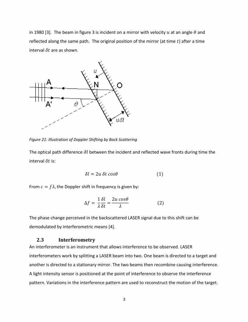
3
in 1980 [3]. The beam in figure 3 is incident on a mirror with velocity 𝑢 at an angle 𝜃 and
reflected along the same path. The original position of the mirror (at time 𝑡) after a time
interval 𝛿𝑡 are as shown.
Figure 21: Illustration of Doppler Shifting by Back Scattering
The optical path difference 𝜕𝑙 between the incident and reflected wave fronts during time the
interval 𝛿𝑡 is:
𝛿𝑙 = 2𝑢 𝛿𝑡 𝑐𝑜𝑠𝜃 (1)
From 𝑐 = 𝑓𝜆, the Doppler shift in frequency is given by:
Δ𝑓 = 1
𝜆
𝛿𝑙
𝛿𝑡=
2𝑢 𝑐𝑜𝑠𝜃
𝜆 (2)
The phase change perceived in the backscattered LASER signal due to this shift can be
demodulated by interferometric means [4].
2.3 Interferometry
An interferometer is an instrument that allows interference to be observed. LASER
interferometers work by splitting a LASER beam into two. One beam is directed to a target and
another is directed to a stationary mirror. The two beams then recombine causing interference.
A light intensity sensor is positioned at the point of interference to observe the interference
pattern. Variations in the interference pattern are used to reconstruct the motion of the target.
4
Generally, interferometers can be classified based on the configuration used into two types:
external interferometry and self-mixing interferometry [5].
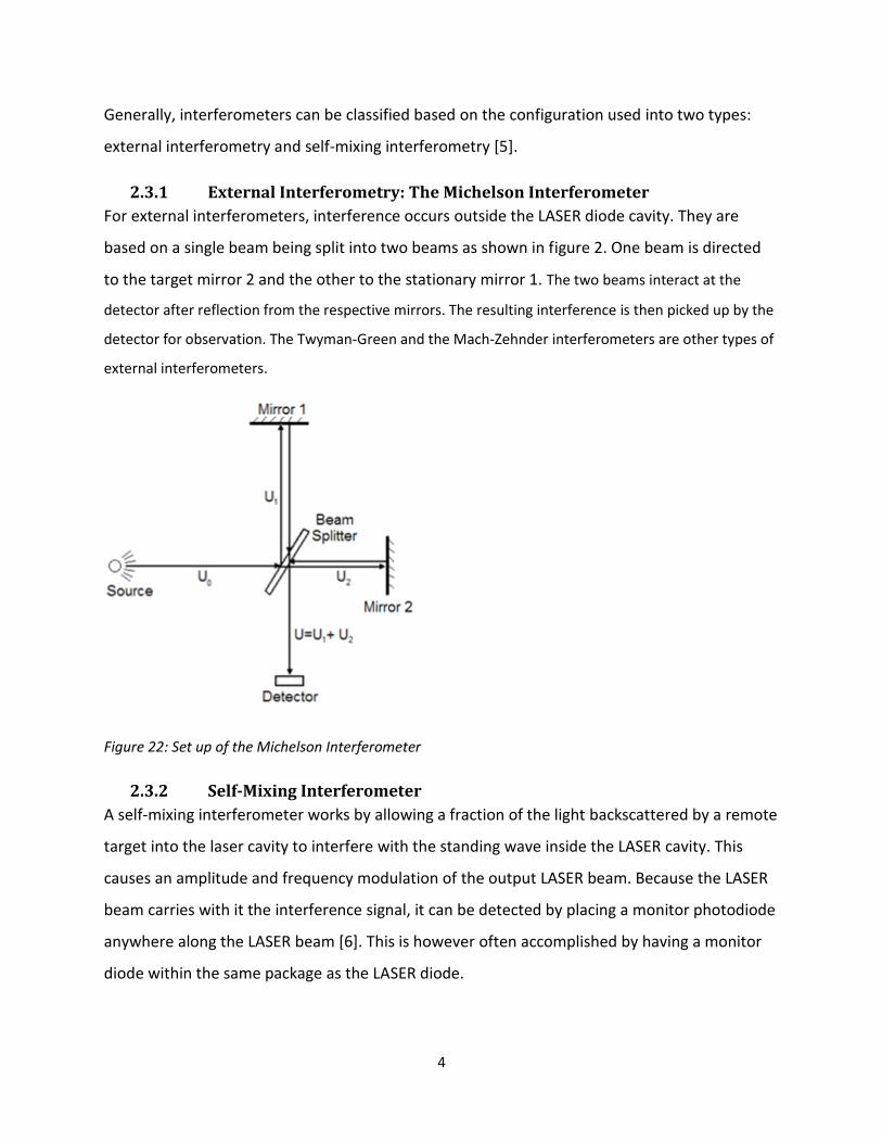
2.3.1 External Interferometry: The Michelson Interferometer
For external interferometers, interference occurs outside the LASER diode cavity. They are
based on a single beam being split into two beams as shown in figure 2. One beam is directed
to the target mirror 2 and the other to the stationary mirror 1. The two beams interact at the
detector after reflection from the respective mirrors. The resulting interference is then picked up by the
detector for observation. The Twyman-Green and the Mach-Zehnder interferometers are other types of
external interferometers.
Figure 22: Set up of the Michelson Interferometer
2.3.2 Self-Mixing Interferometer
A self-mixing interferometer works by allowing a fraction of the light backscattered by a remote
target into the laser cavity to interfere with the standing wave inside the LASER cavity. This
causes an amplitude and frequency modulation of the output LASER beam. Because the LASER
beam carries with it the interference signal, it can be detected by placing a monitor photodiode
anywhere along the LASER beam [6]. This is however often accomplished by having a monitor
diode within the same package as the LASER diode.
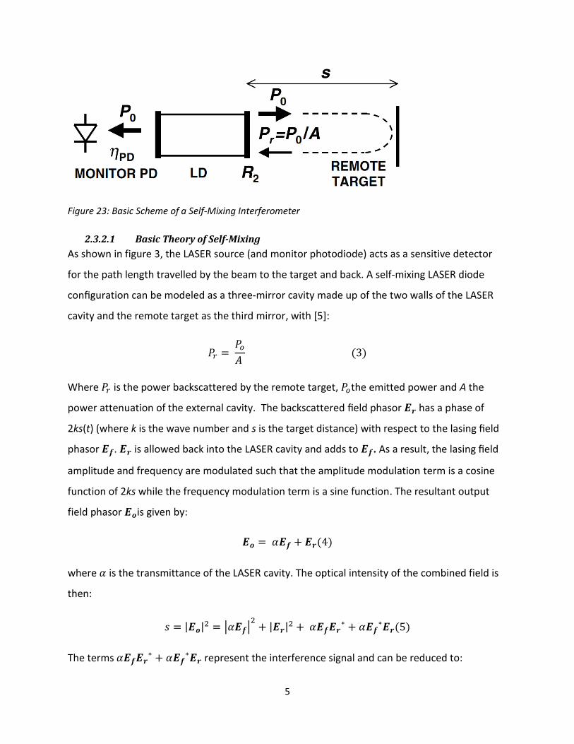
5
Figure 23: Basic Scheme of a Self-Mixing Interferometer
2.3.2.1 Basic Theory of Self-Mixing
As shown in figure 3, the LASER source (and monitor photodiode) acts as a sensitive detector
for the path length travelled by the beam to the target and back. A self-mixing LASER diode
configuration can be modeled as a three-mirror cavity made up of the two walls of the LASER
cavity and the remote target as the third mirror, with [5]:
𝑃𝑟 = 𝑃𝑜
𝐴 (3)
Where 𝑃𝑟 is the power backscattered by the remote target, 𝑃𝑜the emitted power and A the
power attenuation of the external cavity. The backscattered field phasor 𝑬𝒓 has a phase of
2ks(t) (where k is the wave number and s is the target distance) with respect to the lasing field
phasor 𝑬𝒇. 𝑬𝒓 is allowed back into the LASER cavity and adds to 𝑬𝒇. As a result, the lasing field
amplitude and frequency are modulated such that the amplitude modulation term is a cosine
function of 2ks while the frequency modulation term is a sine function. The resultant output
field phasor 𝑬𝒐is given by:
𝑬𝒐 = 𝛼𝑬𝒇 + 𝑬𝒓(4)
where 𝛼 is the transmittance of the LASER cavity. The optical intensity of the combined field is
then:
𝑠 = |𝑬𝒐|2 = |𝛼𝑬𝒇|2
+ |𝑬𝒓|2 + 𝛼𝑬𝒇𝑬𝒓∗ + 𝛼𝑬𝒇
∗𝑬𝒓(5)
The terms 𝛼𝑬𝒇𝑬𝒓∗ + 𝛼𝑬𝒇
∗𝑬𝒓 represent the interference signal and can be reduced to:
6
𝛼𝑬𝒇𝑬𝒓∗ + 𝜶𝑬𝒇
∗𝑬𝒓 = 2𝛼|𝑬𝒇||𝑬𝒓|𝑐𝑜𝑠 𝜔𝑚𝑡 (6)
Where 𝜔𝑚 is the angular beat frequency between the two fields.
Setting 𝑆𝑜 = |𝛼𝑬𝒇|2and for weak feedback (
𝐸𝑟𝐸𝑓
⁄ ≪ 1)
𝑠 = 𝑆𝑜(1 + 𝑚 𝑐𝑜𝑠 𝜔𝑚𝑡) (7)
Where 𝑚 = 2 |𝐸𝑟
𝛼𝐸𝑓⁄ | and |
𝐸𝑟𝐸𝑓
⁄ | is the field amplitude feedback ratio.
Equivalently, the output power density which is the signal detected by the monitor photodiode
is given by
𝑃(∅) = 𝑃𝑜[1 + 𝑚 𝑐𝑜𝑠 𝜔𝑚𝑡] (8)
2.3.2.2 Self-Mixing in a LASER Diode
Any single-mode longitudinal Fabry-Perot (FP) LASER diode can be used for self-mixing as long
as the diode has a side mode suppression larger than 7 to 8 dB [7]. Self-mixing in LASER diodes
differs from the simple three mirror model because of the non-linear nature of the
semiconductor medium that relates both refractive index and optical gain to the injected
carrier density. This means the amplitude modulation term differs from the three mirror cosine
function [8].Lang and Kobayashi developed equations for a complete analysis of the LASER
diode with optical feedback. For sensing applications, steady-state solution for the power
emitted by the LASER diode as given by the equations is [8]:
𝑃(∅) = 𝑃𝑜[1 + 𝑚𝐹(∅)] (9)
Where 𝑃𝑜is the power emitted by the LASER diode without optical feedback,𝐹(∅) is a periodic
function of the phase ∅ = 2𝑘𝑠 and 𝑚 is the modulation index. The modulation index and the
function 𝐹(∅) depend on the feedback regime defined by a parameter known as the feedback
parameter C, which depends on both the amount of feedback and the target distance. The
different feedback regimes are discriminated by the value of the C parameter as shown in table
1 and figure 4:
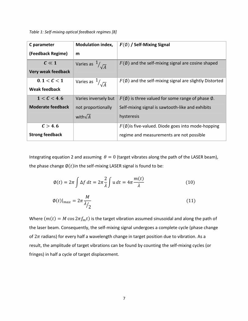
7
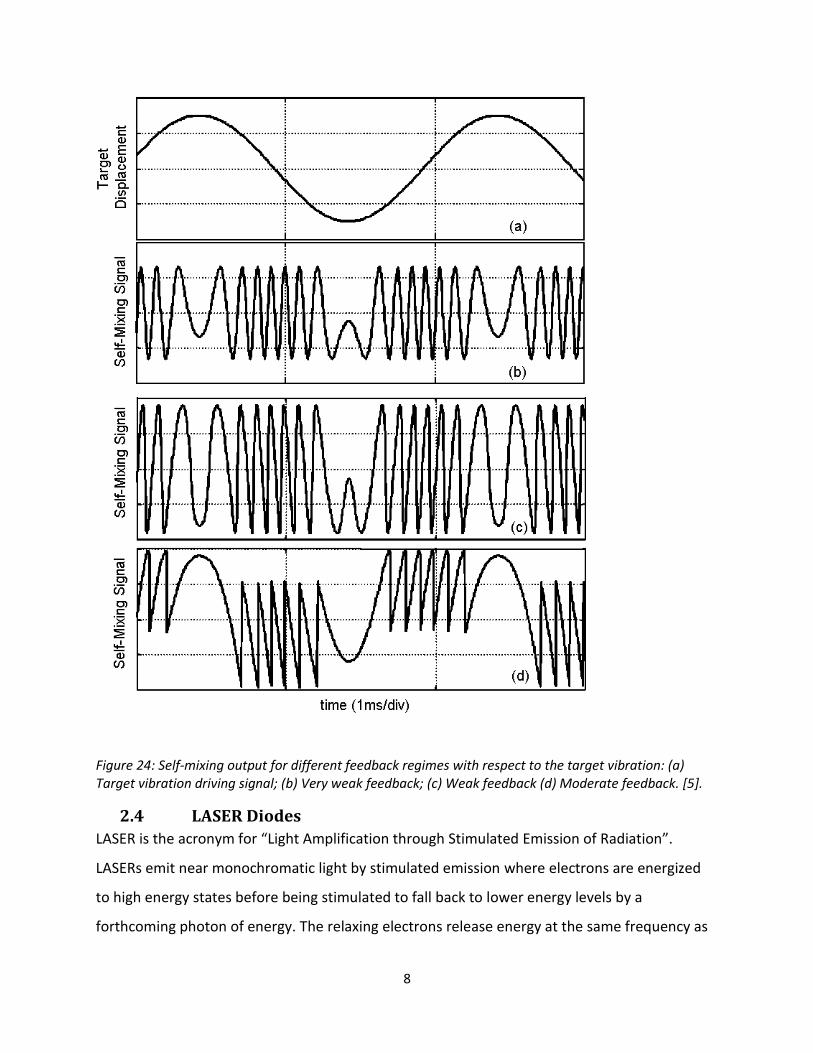
Table 1: Self-mixing optical feedback regimes [8]
C parameter
(Feedback Regime)
Modulation index,
m
𝑭(∅) / Self-Mixing Signal
𝑪 ≪ 𝟏
Very weak feedback
Varies as 1√𝐴
⁄ 𝐹(∅) and the self-mixing signal are cosine shaped
𝟎. 𝟏 < 𝑪 < 𝟏
Weak feedback
Varies as 1√𝐴
⁄ 𝐹(∅) and the self-mixing signal are slightly Distorted
𝟏 < 𝑪 < 𝟒. 𝟔
Moderate feedback
Varies inversely but
not proportionally
with√𝐴
𝐹(∅) is three valued for some range of phase ∅.
Self-mixing signal is sawtooth-like and exhibits
hysteresis
𝑪 > 𝟒. 𝟔
Strong feedback
𝐹(∅)is five-valued. Diode goes into mode-hopping
regime and measurements are not possible
Integrating equation 2 and assuming 𝜃 = 0 (target vibrates along the path of the LASER beam),
the phase change ∅(𝑡)in the self-mixing LASER signal is found to be:
∅(𝑡) = 2𝜋 ∫ Δ𝑓 𝑑𝑡 = 2𝜋2
𝜆∫ u 𝑑𝑡 = 4𝜋
𝑚(𝑡)
𝜆 (10)
∅(𝑡)|𝑚𝑎𝑥 = 2𝜋𝑀
𝜆2⁄
(11)
Where (𝑚(𝑡) = 𝑀 cos 2𝜋𝑓𝑚𝑡) is the target vibration assumed sinusoidal and along the path of
the laser beam. Consequently, the self-mixing signal undergoes a complete cycle (phase change
of 2𝜋 radians) for every half a wavelength change in target position due to vibration. As a
result, the amplitude of target vibrations can be found by counting the self-mixing cycles (or
fringes) in half a cycle of target displacement.
8
Figure 24: Self-mixing output for different feedback regimes with respect to the target vibration: (a) Target vibration driving signal; (b) Very weak feedback; (c) Weak feedback (d) Moderate feedback. [5].
2.4 LASER Diodes
LASER is the acronym for “Light Amplification through Stimulated Emission of Radiation”.
LASERs emit near monochromatic light by stimulated emission where electrons are energized
to high energy states before being stimulated to fall back to lower energy levels by a
forthcoming photon of energy. The relaxing electrons release energy at the same frequency as
9
the photon causing light amplification. A LASER device consists of an optical amplifier that
carries out stimulated emission and a frequency selective resonator that confines and feeds
emitted light back to the amplifier.
The amplifying element in semiconductor LASER diodes is a forward biased P-N junction. A
LASER diode is a current sensitive device, and careful operation is required to prevent damage
to the diode due to large transient as well as sustained currents. Also the frequency output of
the diode is current-dependent, and a stable current is required to ensure stability of the
output frequency [9].
2.5 Photodiodes
Photodiodes are light sensors that generate an electrical signal on illumination with light. The
various types of photodiodes include silicon and germanium P-N photodiodes, P-I-N
photodiodes, avalanche photodiodes (APD) and hetero-junction photodiodes. A photodiode
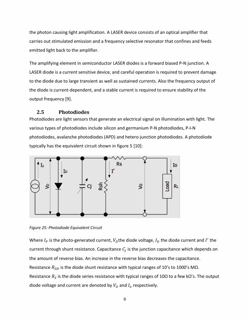
typically has the equivalent circuit shown in figure 5 [10]:
Figure 25: Photodiode Equivalent Circuit
Where 𝐼𝑃 is the photo-generated current, 𝑉𝐷the diode voltage, 𝐼𝐷 the diode current and 𝐼′ the
current through shunt resistance. Capacitance 𝐶𝑗 is the junction capacitance which depends on
the amount of reverse bias. An increase in the reverse bias decreases the capacitance.
Resistance 𝑅𝑆𝐻 is the diode shunt resistance with typical ranges of 10’s to 1000’s MΩ.
Resistance 𝑅𝑆 is the diode series resistance with typical ranges of 10Ω to a few kΩ’s. The output
diode voltage and current are denoted by 𝑉𝑂 and 𝐼𝑜 respectively.
10
Photodiodes can operate in either the photoconductive mode or the photovoltaic mode. In the
photovoltaic mode, the diode is operated with zero voltage bias. This mode eliminates dark
current and is preferred for low noise operation. A large junction capacitance is involved due to
zero bias, which leads to large time constants and it is therefore applicable to slow speed
operation. The photoconductive mode involves reverse biasing the photodiode. This is a fast
mode of operation due to reduced junction capacitances. It however involves large dark
currents.
There are two major noise considerations in photodiode detectors namely shot noise and
Johnson noise. Shot noise depends on the statistical distribution of both the photocurrent and
the dark current. It is the dominating noise when the photodiode is operated in the
photocurrent mode. The magnitude of shot noise is given by:
𝐼𝑠𝑛 = √2𝑞(𝐼𝑃 + 𝐼𝐷)∆𝑓 (12)
Where 𝐼𝑃 is the photocurrent, 𝐼𝐷 the dark current, and ∆𝑓 is the measurement bandwidth.
Johnson noise on the other hand is thermal noise associated with all resistive components. The
photodiode Johnson noise is given by:
𝐼𝑗𝑛 = √4𝑘𝑇∆𝑓
𝑅𝑆𝐻 (13)
Where k is the Boltzmann constant, T absolute temperature in Kelvins and 𝑅𝑆𝐻 is the
photodiode shunt resistance. Johnson noise is the dominant noise in the photovoltaic mode of
a photodiode operation. The total photodiode noise is then given by:
𝐼𝑇 = √𝐼𝑠𝑛2 + 𝐼𝑗𝑛
2 (14)
Equations 12 and 13 show that limiting the bandwidth of measurement, can help minimize the
total photodiode noise.
11
3.0 METHODOLOGY
3.1 Choice of Implementation method
As the project requirements were clear on demodulation of the phase of the LASER signal,
rather than of other LASER parameters such as amplitude, only interferometric methods were
considered. Different types of interferometry were studied and evaluated according to two
categories: external interferometry and the self-mixing interferometry. External
interferometers (such as the Michelson, Twyman-Green and the Mach-Zehnder interferometers)
were found to require a large optical equipment part count including beam splitters and Bragg
cells, on top of separate LASER and photodiodes which made them bulky and part-count
expensive. Moreover, they involve alignment in more than one direction, and hence more
cumbersome to set up. On the other hand, a self-mixing interferometer has the following
advantages:
i. No beam splitters, mirrors and Bragg cells are required, leading to a setup that is
compact, simple and part-count-saving;
ii. No extra photo detector is required as detection is done by a monitor photodiode within
the LASER package
iii. High sensitivity as it can measure vibrations to the order of half a wavelength of the
beam (sub-nanometer lengths). Closed loop techniques can however be employed to
increase sensitivity beyond half a wavelength [11].
iv. It can successfully operate on rough diffusive surfaces
The biggest limitation of the self-mixing set up is the limited target distance as the LASER
regime directly depends on the target distance. To maintain stability, the diode needs to be
operated in moderate feedback regime. As a result, the ratio of the maximum to the minimum
target distance becomes 4.6 in the absence of any light. However, varying the amount of light
fed back (by use of a variable density filter for example), can increase the measurement range
further.
The interferometer was thus chosen to be of the self-mixing architecture. To detect vibrations,
the simple fringe counting method was adopted. This way, the self-mixing concept could be
12
tested and with the resulting insight help in the design of an automated measurement of the
target vibrations. The detector was designed as per the block diagram of figure 6.
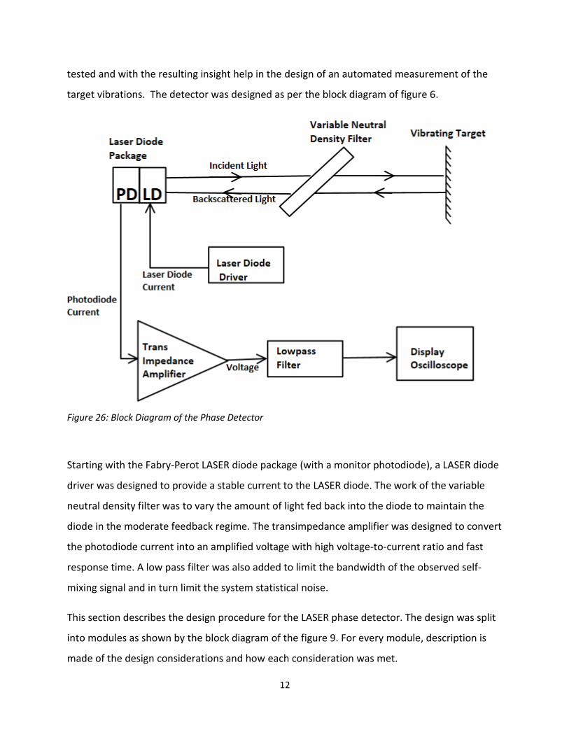
Figure 26: Block Diagram of the Phase Detector
Starting with the Fabry-Perot LASER diode package (with a monitor photodiode), a LASER diode
driver was designed to provide a stable current to the LASER diode. The work of the variable
neutral density filter was to vary the amount of light fed back into the diode to maintain the
diode in the moderate feedback regime. The transimpedance amplifier was designed to convert
the photodiode current into an amplified voltage with high voltage-to-current ratio and fast
response time. A low pass filter was also added to limit the bandwidth of the observed self-
mixing signal and in turn limit the system statistical noise.
This section describes the design procedure for the LASER phase detector. The design was split
into modules as shown by the block diagram of the figure 9. For every module, description is
made of the design considerations and how each consideration was met.
13
As shown in the block diagram, the overall design involved:
i. Choice of the LASER Diode
ii. Design of the LASER diode driver
iii. Design of the Trans Impedance Amplifier
iv. Design of the output filter
3.2 Choice of the LASER diode
Any single longitudinal mode Fabry-Perot LASER diode with an inbuilt monitor photodiode can
be used for self-mixing [7]. Low power was desired to reduce the dangers that come with high
power LASERs. Table 2 shows some of the LASER diodes that can be used for self-mixing
interferometry. Design of the LASER driver in the next section was based on the Hitachi
HL6724MG red LASER diode. However, being that the maximum drive current of the LASER
driver is 50 mA, most of the other diodes can still be reliably driven as well.
Table 2: Some LASER diodes suitable for self-mixing interferometer
Laser Diode Typical Wavelength Output Power Typical operating current
HL6724MG 670 nm 5 mW 35 mA
HL6314MG 635 nm 3 mW 30 mA
DL3149-057 670 nm 7 mW 40 mA
HL6722G 670 nm 5mW 32 mA
3.3 Design of the LASER Diode Driver
A LASER diode is basically a current controlled device that emits highly coherent and
monochromatic light. However, the diode is very sensitive to current disturbances and can
easily get damaged. The LASER driver was thus meant to ensure that:
i. The diode was protected from damage due to excessive transient and sustained
currents
ii. The LASER current was stable to reduce the noise frequency in the diode output
14
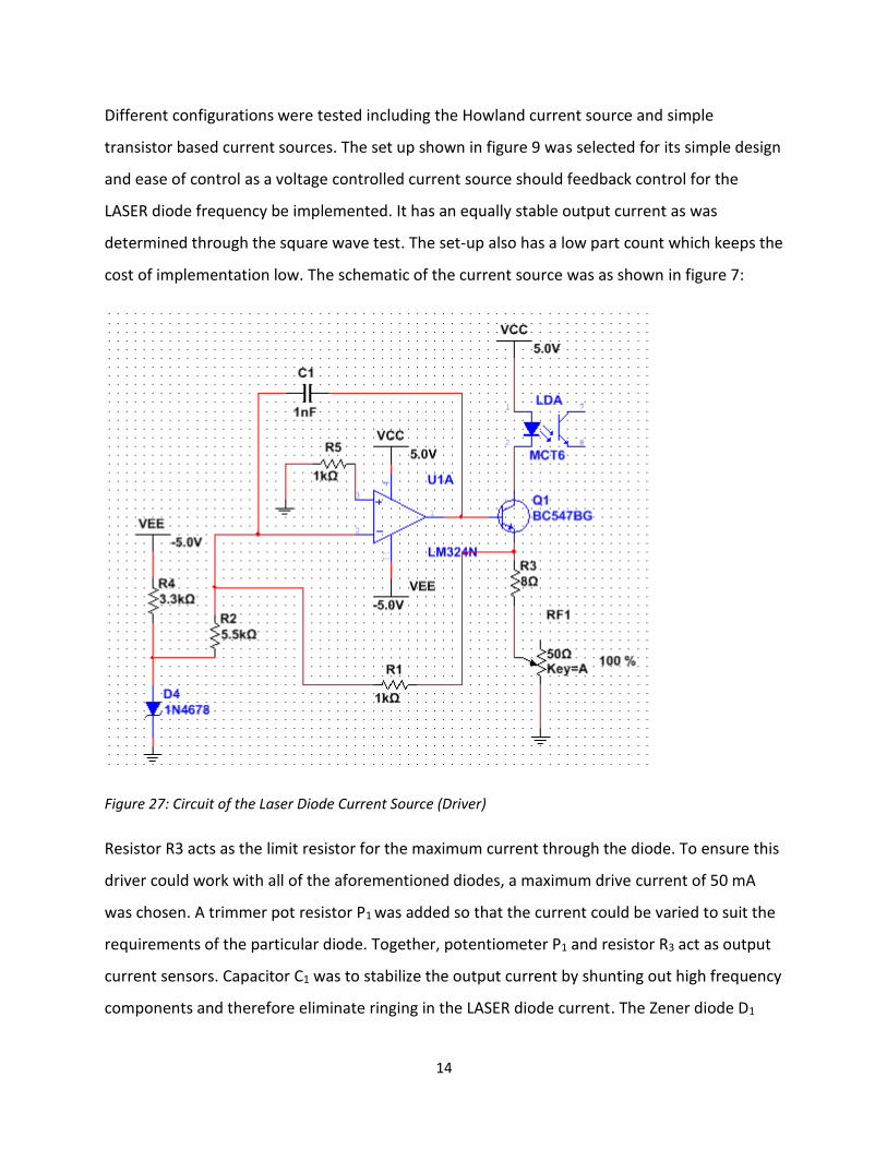
Different configurations were tested including the Howland current source and simple
transistor based current sources. The set up shown in figure 9 was selected for its simple design
and ease of control as a voltage controlled current source should feedback control for the
LASER diode frequency be implemented. It has an equally stable output current as was
determined through the square wave test. The set-up also has a low part count which keeps the
cost of implementation low. The schematic of the current source was as shown in figure 7:
Figure 27: Circuit of the Laser Diode Current Source (Driver)
Resistor R3 acts as the limit resistor for the maximum current through the diode. To ensure this
driver could work with all of the aforementioned diodes, a maximum drive current of 50 mA
was chosen. A trimmer pot resistor P1 was added so that the current could be varied to suit the
requirements of the particular diode. Together, potentiometer P1 and resistor R3 act as output
current sensors. Capacitor C1 was to stabilize the output current by shunting out high frequency
components and therefore eliminate ringing in the LASER diode current. The Zener diode D1
15
was used as a voltage reference while resistors R1 through R3 determined the output current
per unit of reference voltage.
Using an Op Amp with a high open loop gain Ad, the voltage Vo at the output of the Op Amp
with respect to the differential input voltage Vd is:
𝑉𝑜 = 𝐴𝑑𝑉𝑑 (14)
But 𝑉𝑑 = −(𝑉𝑅2 + 𝑉𝑍𝐷) where 𝑉𝑅2 is the voltage across R2 and 𝑉𝑍𝐷 the Zener diode terminal
voltage:
𝑉𝑅2 = 𝐼𝑅2𝑅2 (15)
Because the current through R1, 𝐼𝑅1 = 𝐼𝑅2 (current through R2), the voltage 𝑉𝐸 at the emitter
of transistor Q1 is given by:
𝑉𝐸 = 𝐼𝑅2𝑅1 (16)
𝑉𝑜 = 𝑉𝐸 + 𝑉𝐵𝐸 (17)
Thus the Op Amp input differential voltage becomes:
𝑉𝑑 = 𝑉𝑜
𝐴𝑑=
𝑉𝐸 + 𝑉𝐵𝐸
𝐴𝑑≅ 0 (18)
for large 𝐴𝑑. Thus 𝑉𝑅2 = −𝑉𝑍𝐷 and current through the LASER diode 𝐼𝑜 becomes
𝐼𝑜 = 𝑉𝐸
𝑅3 + 𝑃1=
𝐼𝑅2𝑅1
𝑅3 + 𝑃1=
−𝑉𝑍𝐷
𝑅2𝑅1
𝑅3 + 𝑃1= −𝑉𝑍𝐷
𝑅1
𝑅2(𝑅3 + 𝑃1) (19)
For the current source to work 𝑉𝑍𝐷 was chosen to be negative so that the forward current 𝐼𝑜
through the LASER diode is positive. Small values were chosen for 𝑅3 and 𝑃1 so that they
dropped only a small voltage leaving as much voltage as possible available for the LASER diode.
With a 2.2V Zener diode together with R2 of 5.5 kΩ, R1 of 1 kΩ and R3 of 8 Ω, the LASER diode
driver current limit was thus made:
16
𝐼𝑜 = −𝑉𝑍𝐷
𝑅1
𝑅2(𝑅3 + 𝑃1)= 2.2 𝑉
1 𝑘Ω
(8 Ω)5.5 𝑘Ω= 50 𝑚𝐴
The trimmer potentiometer P1 of value 50 Ω meant that the output current could be varied
down to 5.5 mA.
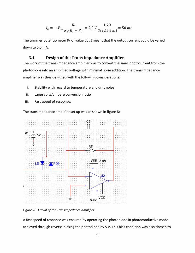
3.4 Design of the Trans Impedance Amplifier
The work of the trans-impedance amplifier was to convert the small photocurrent from the
photodiode into an amplified voltage with minimal noise addition. The trans-impedance
amplifier was thus designed with the following considerations:
i. Stability with regard to temperature and drift noise
ii. Large volts/ampere conversion ratio
iii. Fast speed of response.
The transimpedance amplifier set up was as shown in figure 8:
Figure 28: Circuit of the Transimpedance Amplifier
A fast speed of response was ensured by operating the photodiode in photoconductive mode
achieved through reverse biasing the photodiode by 5 V. This bias condition was also chosen to
17
simplify the design so that the common mode voltage appearing at the input of the
transimpedance Op Amp was zero. Current from the photodiode sees a large impedance on the
non-inverting input of the Op Amp, and is thus forced through resistor RF. Because the non-
inverting input is at virtual ground, a negative voltage proportional to the current is registered
at the Op Amp output. The voltage gain of the amplifier per unit of photodiode current is given
by:
𝐺𝑎𝑖𝑛 (𝑉 𝐴⁄ ) = 𝑅𝐹 (20)
A large resistor RF was needed to provide enough gain for the small photodiode current.
However, this had the effect of increasing thermal noise in the circuit due to the resistor, and
𝑅𝐹 was thus implemented as a trimmer. Resistor 𝑅𝐹 together with stray capacitance in the
circuit creates an oscillatory behavior that causes gain peaking in the circuit and a small
feedback capacitor CF was added to stabilize the transimpedance amplifier. The 3dB
bandwidth𝑓3𝑑𝐵 of the amplifier is then given by [12]:
𝑓3𝑑𝐵(𝐻𝑧) = √𝐺𝐵𝑃
2𝜋𝑅𝐹(𝐶𝐽 + 𝐶𝐹 + 𝐶𝐴) (21)
Where GBP is the Op Amp gain-bandwidth product, 𝐶𝐽 is the junction capacitance of the
photodiode and 𝐶𝐴 is the Op Amp input capacitance.
To realize gains of 106 V/A, RF was selected to be a 1 MΩ trimmer together with 𝐶𝐹 of 2pF. With
this gain, a 10 nA input current would provide a voltage of 10 mV. Most photodiode datasheets
including datasheets for the monitor photodiodes in LASER diodes do not carry information
about the photodiode capacitance. A typical photodiode capacitance of 50pF was used in
determination of the transimpedance bandwidth. However, the actual capacitance was
expected to be lower as the 5V reverse bias on the photodiode lowers this capacitance.
The opa2381 transimpedance amplifier was chosen for the design because it has excellent
desired features, and it was readily available from within the university. The Op Amp has a high
unity-gain bandwidth of 18 MHz, a low input offset current less of than 100 pA but typically of 6
18
pA. The Op Amp also has a low input offset voltage of less than 25 μV and a low drift of 0.1 μV/
oC.
The OPA2381 has a typical input capacitance of 3 pF and a gain bandwidth of 18 MHz. Based on
equation 27, the transimpedance 3 dB bandwidth was found to be:
𝑓3𝑑𝐵(𝐻𝑧) = √18𝑥106
2𝜋𝑥106(50 + 2 + 3)𝑥10−12= 228 𝑘𝐻𝑧
At this bandwidth, and at room temperature 𝑇 of 300 Kelvins, the thermal voltage of the 1 MΩ
resistor was as given by equation28; 𝑘 is the Boltzmann constant.
𝑉𝑟𝑚𝑠 = √4𝑘𝑇𝑅𝐹𝑓3𝑑𝐵 (22)
= √4 ∗ (1.381 ∗ 10−23) ∗ 106 ∗ 228 ∗ 103 ≅ 3.5𝜇V
With such small thermal voltage, the main trade off for a larger resistance was thus the
transimpedance amplifier bandwidth. The offset current of the Op Amp creates a maximum
voltage of 0.1 mV across 𝑅𝐹. The sum of the feedback resistor thermal noise, the Op Amp offset
current and offset voltage noise gives a maximum noise voltage for the transimpedance
amplifier of less than 0.15 mV.
The LASER driver and transimpedance amplifier were tested through simulation as discussed in
the testing section.
3.5 Design of the Low Pass Filter
Typical spectral responses of some silicon photodiodes are as shown in figure 9. Sensitivity of a
photodiode is significant in the visible light range with peak response in the infrared region
(about 900 nm to 1000 nm). In figure 12, QE is the photodiode quantum efficiency, which is the
number of electrons or holes that can contribute to the photodiode current as a fraction of the
number of incident photons.
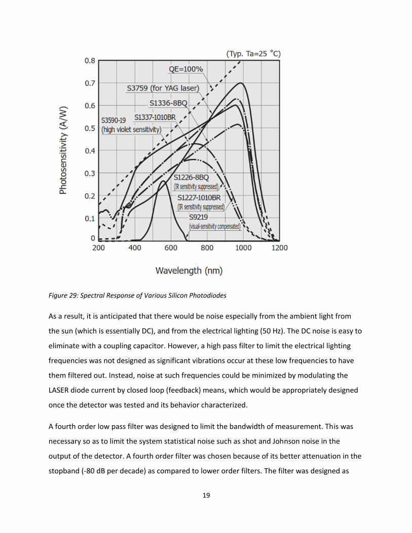
19
Figure 29: Spectral Response of Various Silicon Photodiodes
As a result, it is anticipated that there would be noise especially from the ambient light from
the sun (which is essentially DC), and from the electrical lighting (50 Hz). The DC noise is easy to
eliminate with a coupling capacitor. However, a high pass filter to limit the electrical lighting
frequencies was not designed as significant vibrations occur at these low frequencies to have
them filtered out. Instead, noise at such frequencies could be minimized by modulating the
LASER diode current by closed loop (feedback) means, which would be appropriately designed
once the detector was tested and its behavior characterized.
A fourth order low pass filter was designed to limit the bandwidth of measurement. This was
necessary so as to limit the system statistical noise such as shot and Johnson noise in the
output of the detector. A fourth order filter was chosen because of its better attenuation in the
stopband (-80 dB per decade) as compared to lower order filters. The filter was designed as
20
Bessel type filter to ensure a maximally flat response in the passband. Moreover, the Sallen-Key
topology was selected for its simplicity. A 3 dB cut-off frequency for the low pass filter was set
at 250 kHz to just cater for the bandwidth of the transimpedance of the amplifier. The filter was
designed as a cascade of two second order Sallen-Key filters as shown in figure 10.
A second order lowpass filter is described by the following transfer function in the frequency
domain.
𝐻(𝑓) = 𝐾
(𝑓
𝐹𝑆𝐹 × 𝑓𝑐)
2
+1
𝑄
𝑗𝑓
(𝐹𝑆𝐹 × 𝑓𝑐)+ 1
(23)
Where f is the frequency variable, K is the zero frequency gain, 𝑓𝑐 is the cut-off frequency, 𝑄 is
the filter quality factor and 𝐹𝑆𝐹 is the frequency scaling factor. The passband of the filter is the
frequency range below 𝑓𝑐.
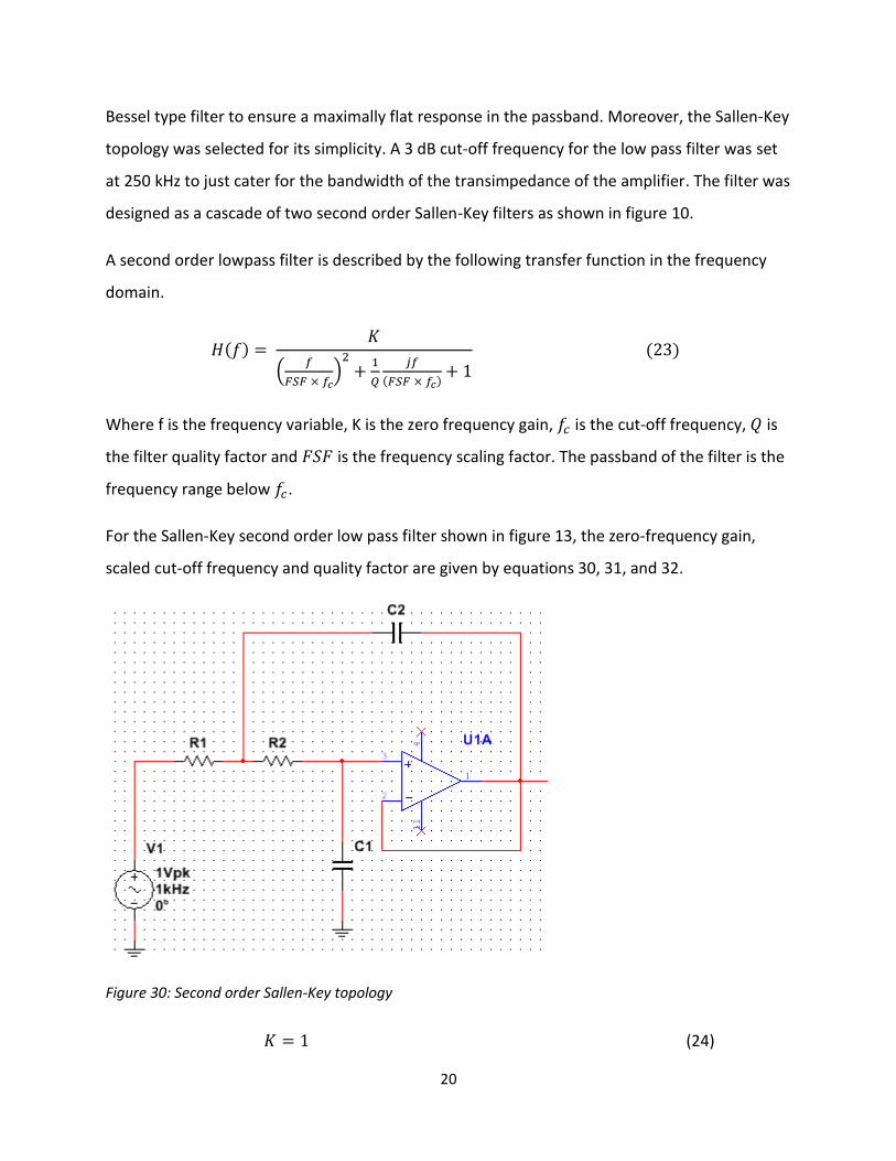
For the Sallen-Key second order low pass filter shown in figure 13, the zero-frequency gain,
scaled cut-off frequency and quality factor are given by equations 30, 31, and 32.
Figure 30: Second order Sallen-Key topology
𝐾 = 1 (24)
21
𝐹𝑆𝐹 × 𝑓𝑐 = 1
2𝜋√𝑅1𝑅2𝐶1𝐶2
(25)
𝑄 =√𝑅1𝑅2𝐶1𝐶2
𝑅1𝐶1 + 𝑅2𝐶1=
1
2𝜋 × 𝐹𝑆𝐹 × 𝑓𝑐(𝑅1𝐶1 + 𝑅2𝐶1) (26)
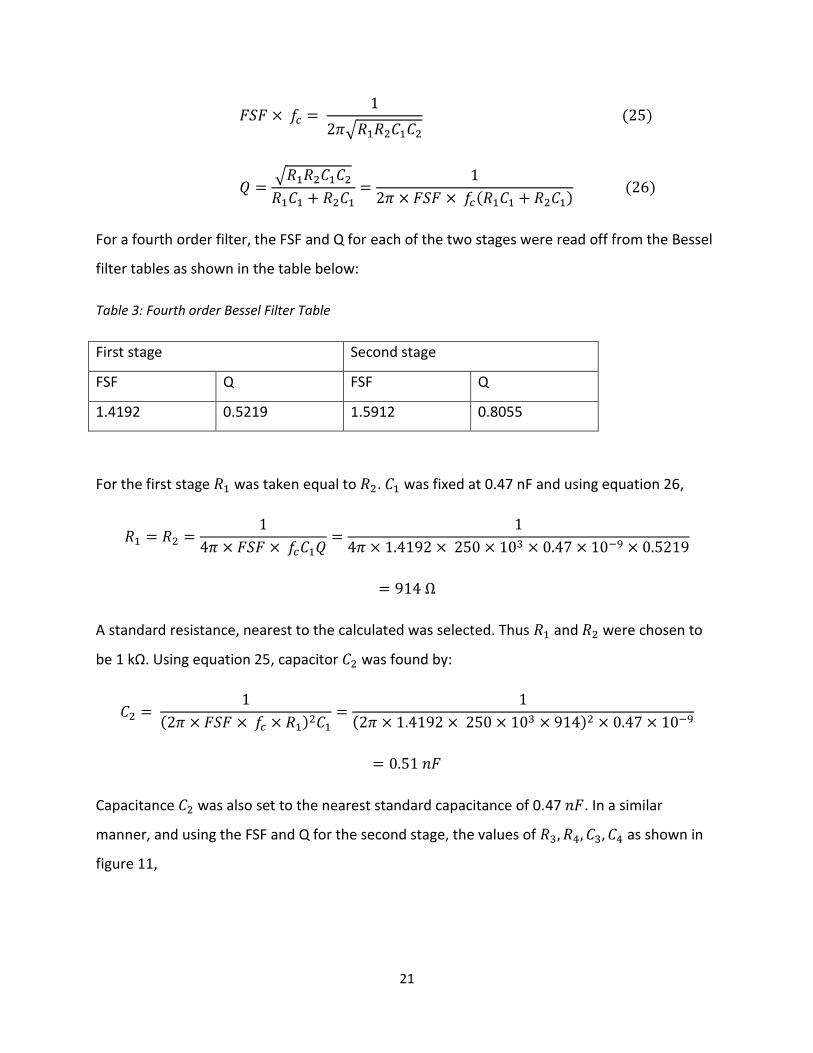
For a fourth order filter, the FSF and Q for each of the two stages were read off from the Bessel
filter tables as shown in the table below:
Table 3: Fourth order Bessel Filter Table
First stage Second stage
FSF Q FSF Q
1.4192 0.5219 1.5912 0.8055
For the first stage 𝑅1 was taken equal to 𝑅2. 𝐶1 was fixed at 0.47 nF and using equation 26,
𝑅1 = 𝑅2 =1
4𝜋 × 𝐹𝑆𝐹 × 𝑓𝑐𝐶1𝑄=
1
4𝜋 × 1.4192 × 250 × 103 × 0.47 × 10−9 × 0.5219
= 914 Ω
A standard resistance, nearest to the calculated was selected. Thus 𝑅1 and 𝑅2 were chosen to
be 1 kΩ. Using equation 25, capacitor 𝐶2 was found by:
𝐶2 = 1
(2𝜋 × 𝐹𝑆𝐹 × 𝑓𝑐 × 𝑅1)2𝐶1=
1
(2𝜋 × 1.4192 × 250 × 103 × 914)2 × 0.47 × 10−9
= 0.51 𝑛𝐹
Capacitance 𝐶2 was also set to the nearest standard capacitance of 0.47 𝑛𝐹. In a similar
manner, and using the FSF and Q for the second stage, the values of 𝑅3, 𝑅4, 𝐶3, 𝐶4 as shown in
figure 11,
22
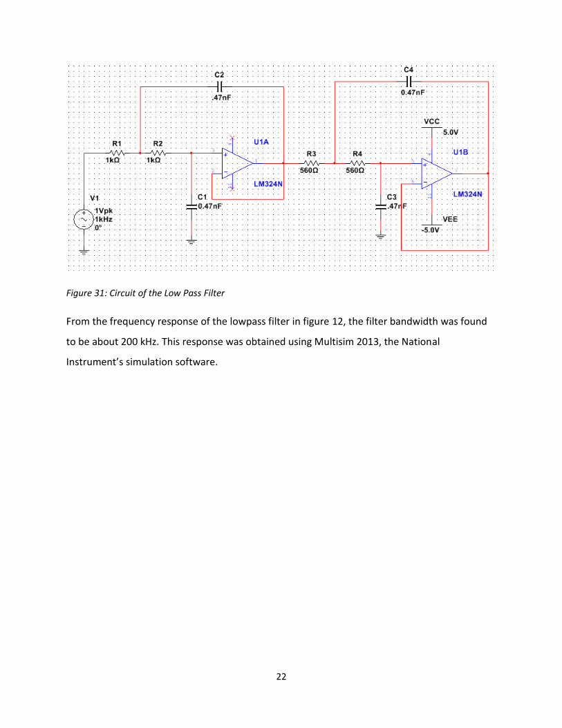
Figure 31: Circuit of the Low Pass Filter
From the frequency response of the lowpass filter in figure 12, the filter bandwidth was found
to be about 200 kHz. This response was obtained using Multisim 2013, the National
Instrument’s simulation software.
23
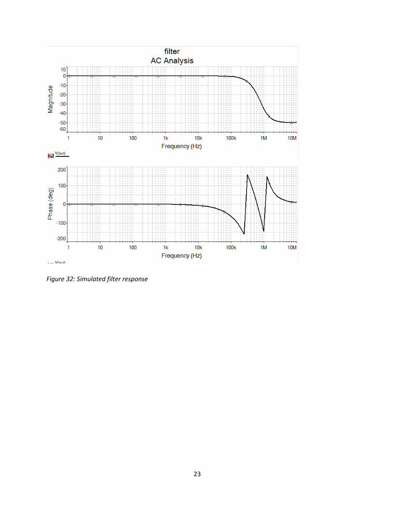
Figure 32: Simulated filter response
24
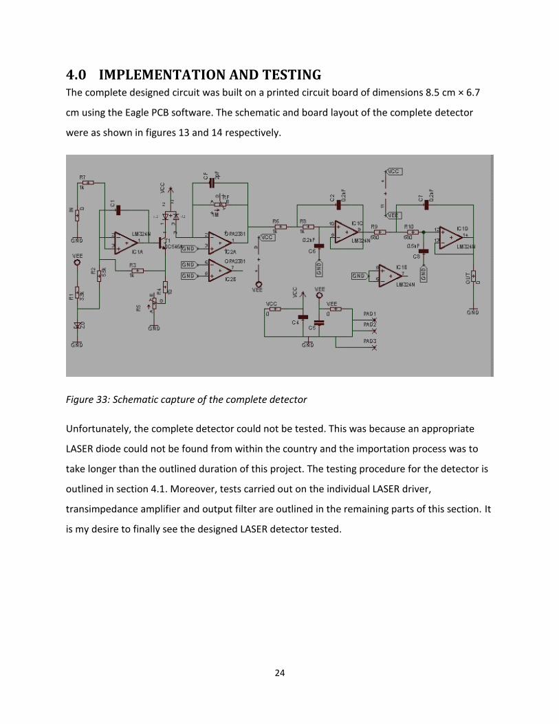
4.0 IMPLEMENTATION AND TESTING The complete designed circuit was built on a printed circuit board of dimensions 8.5 cm × 6.7
cm using the Eagle PCB software. The schematic and board layout of the complete detector
were as shown in figures 13 and 14 respectively.
Figure 33: Schematic capture of the complete detector
Unfortunately, the complete detector could not be tested. This was because an appropriate
LASER diode could not be found from within the country and the importation process was to
take longer than the outlined duration of this project. The testing procedure for the detector is
outlined in section 4.1. Moreover, tests carried out on the individual LASER driver,
transimpedance amplifier and output filter are outlined in the remaining parts of this section. It
is my desire to finally see the designed LASER detector tested.
25
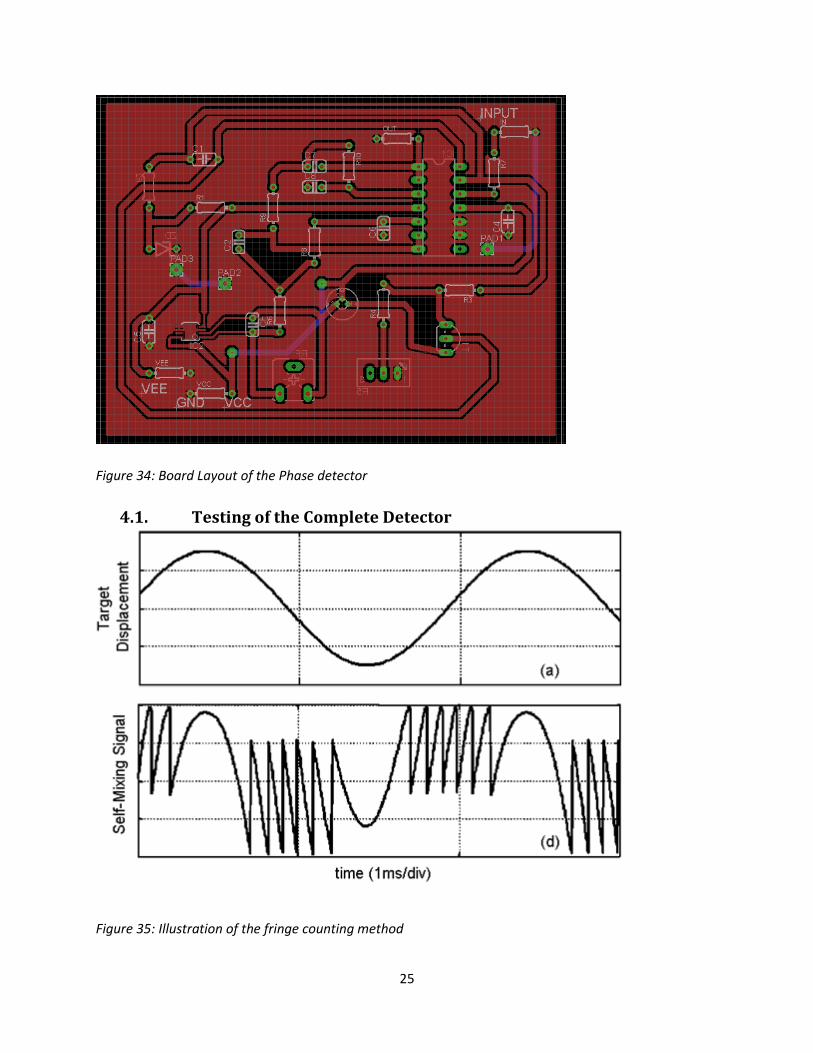
Figure 34: Board Layout of the Phase detector
4.1. Testing of the Complete Detector
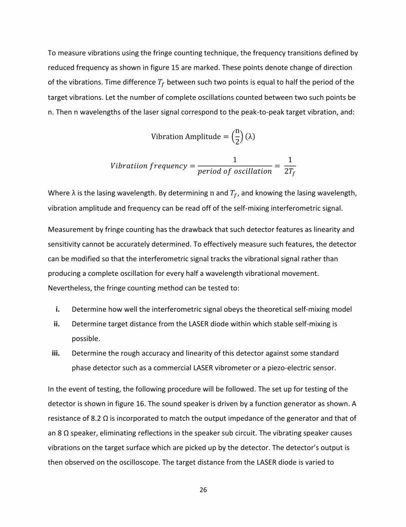
Figure 35: Illustration of the fringe counting method
26
To measure vibrations using the fringe counting technique, the frequency transitions defined by
reduced frequency as shown in figure 15 are marked. These points denote change of direction
of the vibrations. Time difference 𝑇𝑓 between such two points is equal to half the period of the
target vibrations. Let the number of complete oscillations counted between two such points be
n. Then n wavelengths of the laser signal correspond to the peak-to-peak target vibration, and:
Vibration Amplitude = (n
2) (λ)
𝑉𝑖𝑏𝑟𝑎𝑡𝑖𝑖𝑜𝑛 𝑓𝑟𝑒𝑞𝑢𝑒𝑛𝑐𝑦 =1
𝑝𝑒𝑟𝑖𝑜𝑑 𝑜𝑓 𝑜𝑠𝑐𝑖𝑙𝑙𝑎𝑡𝑖𝑜𝑛=
1
2𝑇𝑓
Where λ is the lasing wavelength. By determining n and 𝑇𝑓, and knowing the lasing wavelength,
vibration amplitude and frequency can be read off of the self-mixing interferometric signal.
Measurement by fringe counting has the drawback that such detector features as linearity and
sensitivity cannot be accurately determined. To effectively measure such features, the detector
can be modified so that the interferometric signal tracks the vibrational signal rather than
producing a complete oscillation for every half a wavelength vibrational movement.
Nevertheless, the fringe counting method can be tested to:
i. Determine how well the interferometric signal obeys the theoretical self-mixing model
ii. Determine target distance from the LASER diode within which stable self-mixing is
possible.
iii. Determine the rough accuracy and linearity of this detector against some standard
phase detector such as a commercial LASER vibrometer or a piezo-electric sensor.
In the event of testing, the following procedure will be followed. The set up for testing of the
detector is shown in figure 16. The sound speaker is driven by a function generator as shown. A
resistance of 8.2 Ω is incorporated to match the output impedance of the generator and that of
an 8 Ω speaker, eliminating reflections in the speaker sub circuit. The vibrating speaker causes
vibrations on the target surface which are picked up by the detector. The detector’s output is
then observed on the oscilloscope. The target distance from the LASER diode is varied to
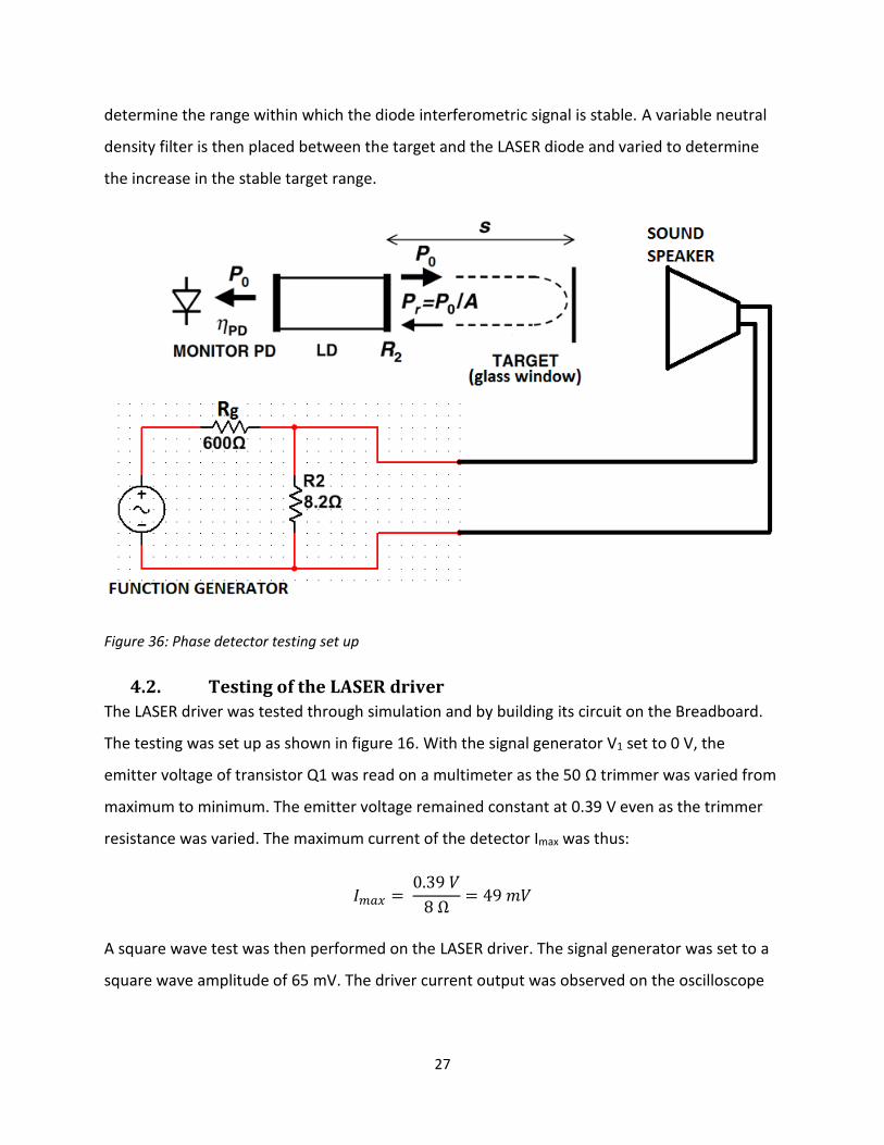
27
determine the range within which the diode interferometric signal is stable. A variable neutral
density filter is then placed between the target and the LASER diode and varied to determine
the increase in the stable target range.
Figure 36: Phase detector testing set up
4.2. Testing of the LASER driver
The LASER driver was tested through simulation and by building its circuit on the Breadboard.
The testing was set up as shown in figure 16. With the signal generator V1 set to 0 V, the
emitter voltage of transistor Q1 was read on a multimeter as the 50 Ω trimmer was varied from
maximum to minimum. The emitter voltage remained constant at 0.39 V even as the trimmer
resistance was varied. The maximum current of the detector Imax was thus:
𝐼𝑚𝑎𝑥 = 0.39 𝑉
8 Ω= 49 𝑚𝑉
A square wave test was then performed on the LASER driver. The signal generator was set to a
square wave amplitude of 65 mV. The driver current output was observed on the oscilloscope
28
as the voltage drop across the 8Ω resistor R3 and the trimmer RF1. The input voltage and output
current waveforms are shown in figure 18.
Figure 37: Testing circuit of the LASER driver
The output current waveform in figure 18 shows no ringing or oscillations. Instead, the
smoothing at the voltage transitions shows that very high frequency components are filtered
out. Again, the rise time of the output current waveform is less than a microsecond, showing
that the LASER driver can handle feedback signals of over 1 MHz. Being that the bandwidth of
the system is 250 kHz, the LASER driver has enough bandwidth for the design of a feedback
controller based on the detector output.
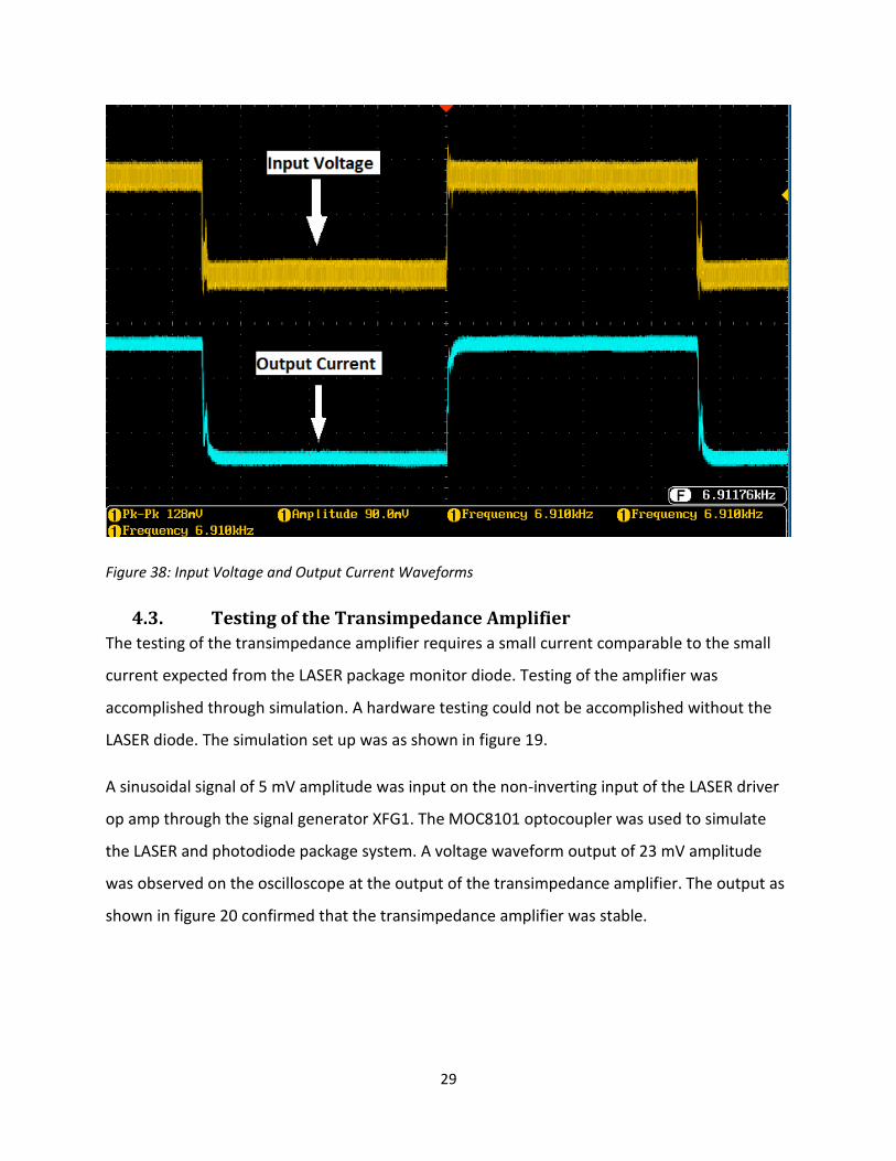
29
Figure 38: Input Voltage and Output Current Waveforms
4.3. Testing of the Transimpedance Amplifier
The testing of the transimpedance amplifier requires a small current comparable to the small
current expected from the LASER package monitor diode. Testing of the amplifier was
accomplished through simulation. A hardware testing could not be accomplished without the
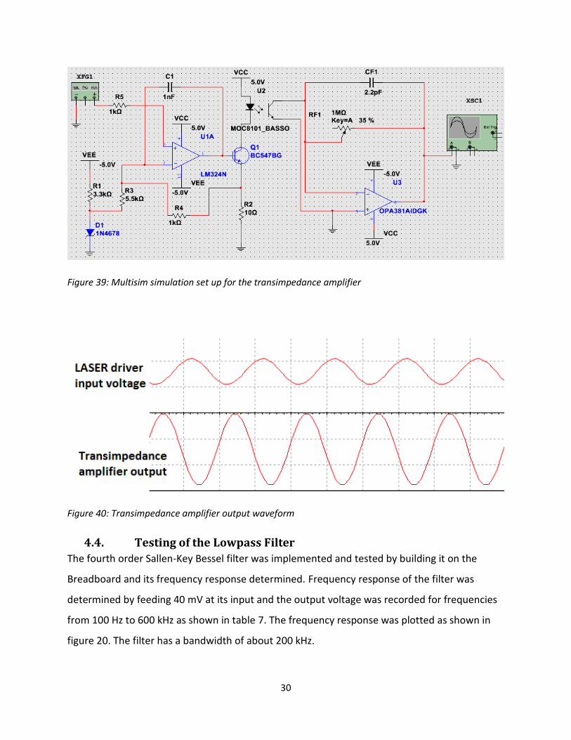
LASER diode. The simulation set up was as shown in figure 19.
A sinusoidal signal of 5 mV amplitude was input on the non-inverting input of the LASER driver
op amp through the signal generator XFG1. The MOC8101 optocoupler was used to simulate
the LASER and photodiode package system. A voltage waveform output of 23 mV amplitude
was observed on the oscilloscope at the output of the transimpedance amplifier. The output as
shown in figure 20 confirmed that the transimpedance amplifier was stable.
30
Figure 39: Multisim simulation set up for the transimpedance amplifier
Figure 40: Transimpedance amplifier output waveform
4.4. Testing of the Lowpass Filter
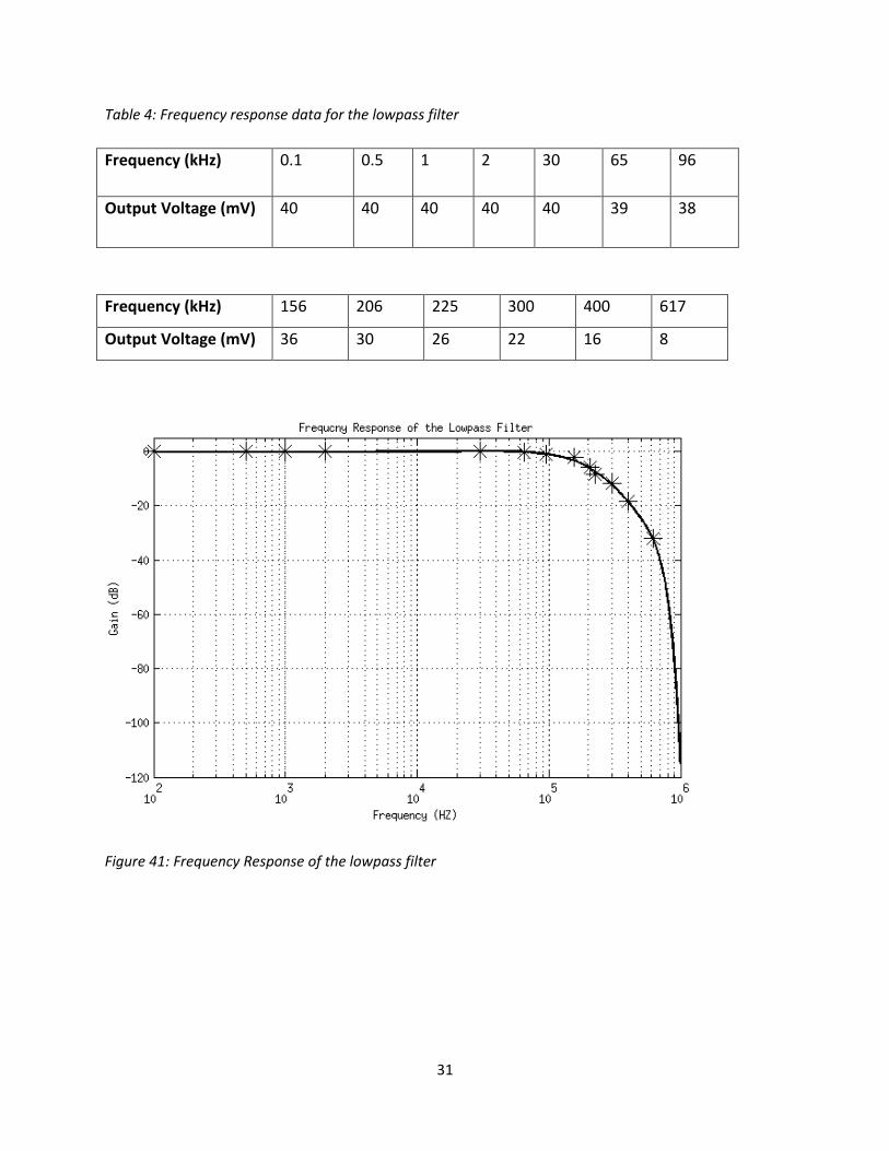
The fourth order Sallen-Key Bessel filter was implemented and tested by building it on the
Breadboard and its frequency response determined. Frequency response of the filter was
determined by feeding 40 mV at its input and the output voltage was recorded for frequencies
from 100 Hz to 600 kHz as shown in table 7. The frequency response was plotted as shown in
figure 20. The filter has a bandwidth of about 200 kHz.
31
Table 4: Frequency response data for the lowpass filter
Frequency (kHz) 0.1 0.5 1 2 30 65 96
Output Voltage (mV) 40 40 40 40 40 39 38
Frequency (kHz) 156 206 225 300 400 617
Output Voltage (mV) 36 30 26 22 16 8
Figure 41: Frequency Response of the lowpass filter
32
5.0 DISCUSSION A 200 kHz bandwidth LASER phase perturbation demodulator was designed and built. The
detector was based on self-mixing interferometry and achieved phase demodulation by the
fringe counting method. Its component circuits namely the LASER driver, the transimpedance
amplifier and the output lowpass filter were tested and verified to meet their design
specifications. Although a single longitudinal mode LASER diode appropriate for self-mixing
could not be acquired in time to test the detector for its phase demodulation characteristics,
the testing procedure was presented. The detector is still far from automated, requiring manual
counting to convert fringes into the equivalent vibration amplitude and frequency. Moreover,
its sensitivity is based on the lasing wavelength and can only be used for measurement of
vibration amplitudes greater than half the lasing wavelength.
33
6.0 CONCLUSION The main objective of the project was to build a phase detector for demodulation of the LASER
signal phase perturbations and use the phase detector to observe small vibrations on a glass
window. Theoretical background was developed and the detector designed and implemented.
The detector is however not a finished product. Instead, it forms the basis upon which more
control and automation of the phase demodulation mechanism can be built. The use of a self-
mixing interferometer which is suited for closed loop feedback control further adds to the
reasons to not only fully test this detector but also improve upon it.
34
7.0 RECOMMENDATIONS The developed detector can be improved in a few areas. It can be improved upon to track the
vibration signal instead of outputting a full oscillation for every half a wavelength target
vibration. This can be achieved through open loop techniques as well as phase locking through
a phase locked loop (PLL). Having made the LASER driver a voltage controlled current source,
interfacing with the PLL is made simpler. The same feedback phase locked loop can be used to
modulate the lasing current and eliminate dependence of the detector sensitivity and range on
the lasing wavelength. This would serve to increase the target range and improve stability of
the LASER diode current, hence its linewidth thereby improving the sensitivity of the diode
beyond half a wavelength of the lasing signal.
35
8.0 REFERENCES [1] A. L. Kachelmyer and K.I.Schultz, “LASER Vibration Sensing”, the Lincoln Laboratory
Journal, Vol. 8, No. 1, 1995
[2] P.R. Kaczmarek et.al, “LASER Doppler Vibrometry with Acoustooptic Frequency
shift”, Optica Applicata, Vol. XXXIV, No. 3, 2004
[3] L. E. Drain, The LASER Doppler Technique, 1980, New York: J. Wiley
[4] A. Y. Karasik, B. S. Rinkevichius and V. A. Zubov, Laser interferometry principles,
Advances in science and technology, 1995, Boca Raton: Mir Publishers, CRC Press
[5] T. Bosch, N. Servagent and S. Donati, “Optical feedback interferometry for sensing
application”, Optical Engineering 40(1) 207, 2001.
[6] S. Donati, Electro-optical instrumentation : sensing and measuring with lasers, 2004
Upper Saddle River, NJ: Prentice Hall
[7] Pawan Kumar Shrestha, “Self Mixing Laser Interferometry: A thesis submitted to the
University of Waikato for the degree of Masters of Engineering”, The University
of Waikato, Hamilton, New Zealand, 2010
[8] R. Lang and K. Kobayashi, “External optical feedback effects on semiconductor
injection laser properties”, IEEE Journal of Quantum Electronics QE-16(3), 1980,
pp. 347-55.
[9] R. Wolfson and J. M. Pasachoff, Physics: extended with modern physics, 1990,
Glenview, III: Scott, Foresman/Little, Brown HigherEducation
[10] S. Donati, Photodetectors, Devices, Circuits and Applications, 2000, Englewood
Cliffs NJ, Prentice-Hall
[11] G. Giuliani, M. Norgia, S. Donati and T. Bosch, “Laser diode self-mixing technique for
sensing applications”, Journal of Optics A; Pure and Applied Optics 4(2002), 2002
pp. 283-294
[12] S. Franco, Design with Operational Amplifiers and Analog Integrated Circuits, 3rd ed.
McGraw-Hill, 2002
Recommended