www.ti.com
FEATURES
TMS470R1A25616/32-Bit RISC Flash Microcontroller
SPNS100A–NOVEMBER 2004–REVISED SEPTEMBER 2005
• Asynchronous/Isosynchronous Modes• High-Performance Static CMOS Technology – Standard CAN Controller (SCC)• TMS470R1x 16/32-Bit RISC Core • 16-Mailbox Capacity
(ARM7TDMI™) • Fully Compliant With CAN Protocol,– 24-MHz System Clock (48-MHz Pipeline Version 2.0B
Mode) – Class II Serial Interface (C2SIb)– Independent 16/32-Bit Instruction Set • Two Selectable Data Rates– Open Architecture With Third-Party Support • Normal Mode 10.4 Kbps and 4X Mode 41.6– Built-In Debug Module Kbps– Big-Endian Format Utilized • High-End Timer (HET)
• Integrated Memory – 16 Programmable I/O Channels:– 256K-Byte Program Flash • 14 High-Resolution Pins
• One Bank With 14 Contiguous Sectors • 2 Standard-Resolution Pins• Internal State Machine for Programming – High-Resolution Share Feature (XOR)
and Erase – High-End Timer RAM– 12K-Byte Static RAM (SRAM) • 64-Instruction Capacity
• Operating Features • 10-Bit Multi-Buffered ADC (MibADC)– Core Supply Voltage (VCC): 1.81 V–2.05 V 16-Channel– I/O Supply Voltage (VCCIO): 3.0 V–3.6 V – 64-Word FIFO Buffer– Low-Power Modes: STANDBY and HALT – Single- or Continuous-Conversion Modes– Extended Industrial Temperature Ranges – 1.55 µs Minimum Sample and Conversion
Time• 470+ System Module– Calibration Mode and Self-Test Features– 32-Bit Address Space Decoding
• 8 External Interrupts– Bus Supervision for Memory andPeripherals • Flexible Interrupt Handling
– Analog Watchdog (AWD) Timer • 11 Dedicated GIO Pins, 1 Input-Only GIO Pin,and 38 Additional Peripheral I/Os (A256)– Real-Time Interrupt (RTI)
• External Clock Prescale (ECP) Module– System Integrity and Failure Detection– Programmable Low-Frequency External• Zero-Pin Phase-Locked Loop (ZPLL)-Based
Clock (CLK)Clock Module With Prescaler• Compatible ROM Device– Multiply-by-4 or -8 Internal ZPLL Option• On-Chip Scan-Base Emulation Logic, IEEE– ZPLL Bypass Mode
Standard 1149.1 (JTAG) Test-Access Port (1)• Six Communication Interfaces:
• 100-Pin Plastic Low-Profile Quad Flatpack (PZ– Two Serial Peripheral Interfaces (SPIs)Suffix)
• 255 Programmable Baud Rates(1) The test-access port is compatible with the IEEE Standard– Two Serial Communications Interfaces
1149.1-1990, IEEE Standard Test-Access Port and Boundary(SCIs)Scan Architecture. Boundary scan is not supported on this
• 224 Selectable Baud Rates device.
Please be aware that an important notice concerning availability, standard warranty, and use in critical applications of TexasInstruments semiconductor products and disclaimers thereto appears at the end of this data sheet.
ARM7TDMI is a trademark of Advanced RISC Machines Limited (ARM).All trademarks are the property of their respective owners.
PRODUCTION DATA information is current as of publication date. Copyright © 2004–2005, Texas Instruments IncorporatedProducts conform to specifications per the terms of the TexasInstruments standard warranty. Production processing does notnecessarily include testing of all parameters.
www.ti.com
76
77
78
79
80
81
82
83
84
85
86
87
88
89
90
91
92
93
94
95
96
97
98
99
100
50
49
48
47
46
45
44
43
42
41
40
39
38
37
36
35
34
33
32
31
30
29
28
27
26
75 74 73 72 71 70 69 68 67 66 65 64 63 62 61 60 59 58 57 56 55 54 53 52 51
1 2 3 4 5 6 7 8 9 10 11 12 13 14 15 16 17 18 19 20 21 22 23 24 25
ADIN[11]
ADIN[14]
ADIN[10]
ADIN[13]
ADIN[9]
ADIN[12]
ADREFHI
ADREFLO
VCCAD
VSSAD
TMS
TMS2
VSS
VCC
HET[0]
VSS
VCC
FLTP2
FLTP1
VCCP
HET[2]
HET[4]
HET[6]
HET[7]
AWD
HET[18]
HET[20]
HET[21]
SPI2SCS
SPI2ENA
SPI2SOMI
SPI2SIMO
SPI2CLK
VCC
VSS
C2SIRX
C2SITX
C2SILPN
HET[24]
HET[31]
SCI2TX
SCI2RX
GIOA[3]/INT3
GIOA[2]/INT2
GIOA[1]/INT1/ECLK
GIOA[0]/INT0(A)
TEST
TRST
SP
I1E
NA
SP
I1S
CS
SP
I1S
IMO
SP
I1S
OM
I
SP
I1C
LK VS
SO
SC
OU
T
OS
CIN
VC
C
RS
T
VS
SIO
V
CC
IOG
IOB
[3]
GIO
B[2
]
GIO
B[1
]
GIO
B[0
]
HE
T[1
3]
HE
T[1
2]
HE
T[1
1]
HE
T[1
0]
PO
RR
ST
GIO
A[7
]/IN
T7
GIO
A[6
]/IN
T6
GIO
A[5
]/IN
T5
GIO
A[4
]/IN
T4
AD
IN[0
]
AD
IN[1
]
AD
IN[2
]
AD
IN[3
]
AD
IN[4
]
AD
IN[1
5]
AD
IN[5
]
AD
IN[6
]
AD
IN[7
]
AD
EV
T
VC
C
VS
S
SC
I1R
X
SC
I1T
X
SC
I1C
LK
CA
NS
TX
CA
NS
RX
CLK
OU
T
VC
CIO
VS
SIO
HE
T[8
]
TC
K
TD
O
TD
I
PLL
DIS
ADIN[8]
HET[19]
DESCRIPTION
TMS470R1A25616/32-Bit RISC Flash MicrocontrollerSPNS100A–NOVEMBER 2004–REVISED SEPTEMBER 2005
TMS470R1A256 100-PIN PZ PACKAGE (TOP VIEW)
A. GIOA[0]/INT0 (pin 28) is an input-only GIO pin.
The TMS470R1A256 (1) devices are members of the Texas Instruments TMS470R1x family of general-purpose16/32-bit reduced instruction set computer (RISC) microcontrollers. The A256 microcontroller offers highperformance utilizing the high-speed ARM7TDMI 16/32-bit RISC central processing unit (CPU), resulting in ahigh instruction throughput while maintaining greater code efficiency. The ARM7TDMI 16/32-bit RISC CPU viewsmemory as a linear collection of bytes numbered upwards from 0. The TMS470R1A256 utilizes the big-endianformat where the most significant byte of a word is stored at the lowest numbered byte and the least significantbyte at the highest numbered byte.
High-end embedded control applications demand more performance from their controllers while maintaining lowcosts. The A256 RISC core architecture offers solutions to these performance and cost demands whilemaintaining low power consumption.(1) Throughout the remainder of this document, the TMS470R1A256 device name will be referred to as either the full device name,
TMS470R1A256, or as A256.
2
www.ti.com
TMS470R1A25616/32-Bit RISC Flash Microcontroller
SPNS100A–NOVEMBER 2004–REVISED SEPTEMBER 2005
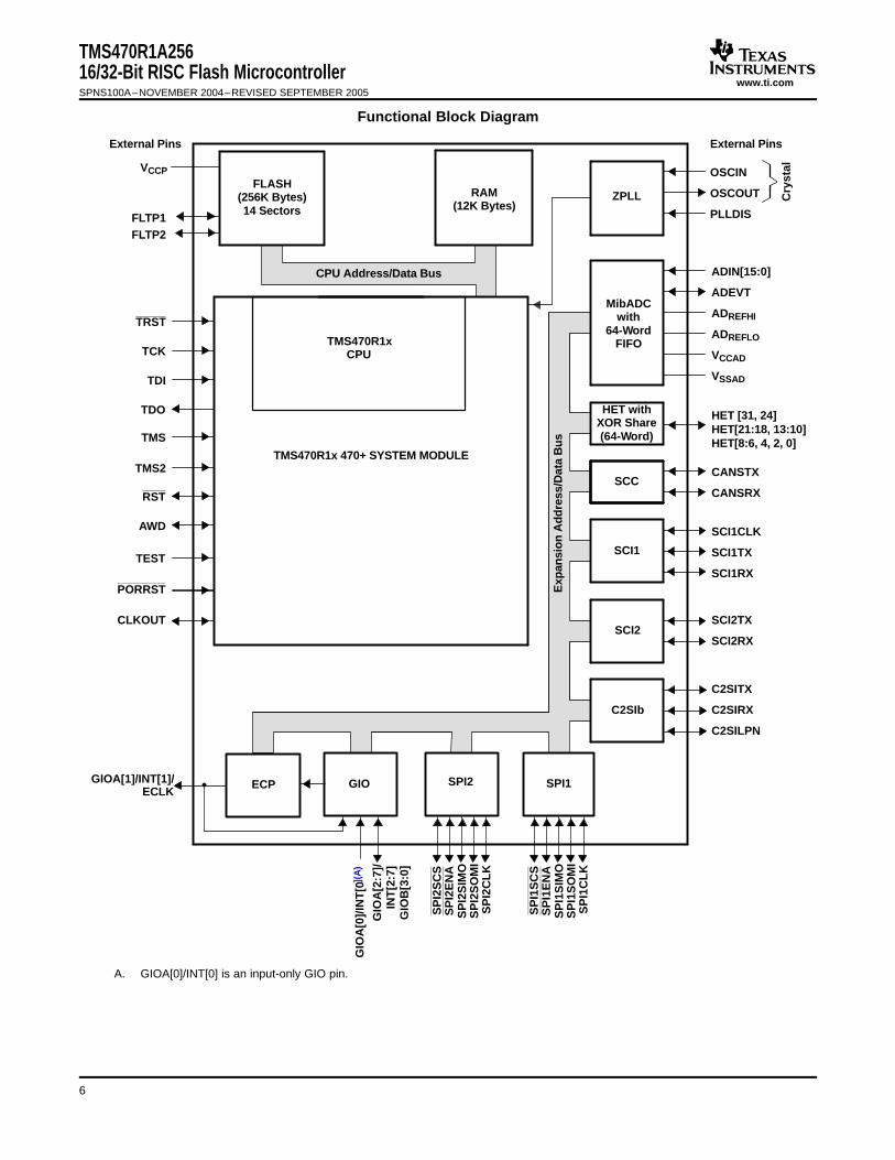
The A256 device contains the following:• ARM7TDMI 16/32-Bit RISC CPU• TMS470R1x system module (SYS) with 470+ enhancements• 256K-byte flash• 12K-byte SRAM• Zero-pin phase-locked loop (ZPLL) clock module• Analog watchdog (AWD) timer• Real-time interrupt ( RTI) module• Two serial peripheral interface (SPI) modules• Two serial communications interface (SCI) modules• Standard CAN controller (SCC)• Class II serial interface (C2SIb)• 10-bit multi-buffered analog-to-digital converter (MibADC), 16-input channels• High-end timer (HET) controlling 16 I/Os• External clock prescale (ECP) module• Up to 49 I/O pins and 1 input-only pin
The functions performed by the 470+ system module (SYS) include:• Address decoding• Memory protection• Memory and peripherals bus supervision• Reset and abort exception management• Prioritization for all internal interrupt sources• Device clock control• Parallel signature analysis (PSA)• This data sheet includes device-specific information such as memory and peripheral select assignment,
interrupt priority, and a device memory map. For a more detailed functional description of the SYS module,see the TMS470R1x System Module Reference Guide (literature number SPNU189).
The A256 memory includes general-purpose SRAM supporting single-cycle read/write accesses in byte,half-word, and word modes.
The flash memory on this device is a nonvolatile, electrically erasable and programmable memory implementedwith a 32-bit-wide data bus interface. In pipeline mode, the flash operates with a system clock frequency of up to48 MHz. In normal mode, the flash operates with a system clock frequency of up to 24 MHz. For more detailedinformation on the flash, see the F05 flash section of this data sheet and the TMS470R1x F05 Flash ReferenceGuide (literature number SPNU213).
The A256 device has six communication interfaces: two SPIs, two SCIs, an SCC, and a C2SIb. The SPI providesa convenient method of serial interaction for high-speed communications between similar shift-register typedevices. The SCI is a full-duplex, serial I/O interface intended for asynchronous communication between theCPU and other peripherals using the standard non-return-to-zero (NRZ) format. The SCC uses a serial,multimaster communication protocol that efficiently supports distributed real-time control with robust communi-cation rates of up to 1 megabit per second (Mbps). The SCC is ideal for applications operating in noisy andharsh environments (e.g., industrial fields) that require reliable serial communication or multiplexed wiring. TheC2SIb allows the A256 to transmit and receive messages on a class II network following an SAE J1850 (2)
standard. For more detailed functional information on the SPI, SCI, and SCC peripherals, see the specificreference guides (literature numbers SPNU195, SPNU196, and SPNU197, respectively). For more detailedfunctional information on the C2SIb peripheral, see the TMS470R1x Class II Serial Interface B (C2SIb)Reference Guide (literature number SPNU214).(2) SAE Standard J1850 Class B Data Communication Network Interface
3
www.ti.com
TMS470R1A25616/32-Bit RISC Flash MicrocontrollerSPNS100A–NOVEMBER 2004–REVISED SEPTEMBER 2005
The HET is an advanced intelligent timer that provides sophisticated timing functions for real-time applications.The timer is software-controlled, using a reduced instruction set, with a specialized timer micromachine and anattached I/O port. The HET can be used for compare, capture, or general-purpose I/O. It is especially well suitedfor applications requiring multiple sensor information and drive actuators with complex and accurate time pulses.For more detailed functional information on the HET, see the TMS470R1x High-End Timer (HET) ReferenceGuide (literature number SPNU199).
The A256 HET peripheral contains the XOR-share feature. This feature allows two adjacent HET high-resolutionchannels to be XORed together, making it possible to output smaller pulses than a standard HET. For moredetailed information on the HET XOR-share feature, see the TMS470R1x High-End Timer (HET) ReferenceGuide (literature number SPNU199).
The A256 device has a 10-bit-resolution sample-and-hold MibADC. The MibADC channels can be convertedindividually or can be grouped by software for sequential conversion sequences. There are three separategroupings, two of which are triggerable by an external event. Each sequence can be converted once whentriggered or configured for continuous conversion mode. For more detailed functional information on the MibADC,see the TMS470R1x Multi-Buffered Analog-to-Digital Converter (MibADC) Reference Guide (literature numberSPNU206).
The zero-pin phase-locked loop (ZPLL) clock module contains a phase-locked loop, a clock-monitor circuit, aclock-enable circuit, and a prescaler (with prescale values of 1–8). The function of the ZPLL is to multiply theexternal frequency reference to a higher frequency for internal use. The ZPLL provides ACLK to the system(SYS) module. The SYS module subsequently provides the system clock (SYSCLK), real-time interrupt clock(RTICLK), CPU clock (MCLK), and peripheral interface clock (ICLK) to all other A256 device modules. For moredetailed functional information on the ZPLL, see the TMS470R1x Zero-Pin Phase Locked Loop (ZPLL) ClockModule Reference Guide (literature number SPNU212).
NOTE:
ACLK should not be confused with the MibADC internal clock, ADCLK. ACLK is thecontinuous system clock from an external resonator/crystal reference.
The A256 device also has an external clock prescaler (ECP) module that when enabled, outputs a continuousexternal clock (ECLK) on a specified GIO pin. The ECLK frequency is a user-programmable ratio of theperipheral interface clock (ICLK) frequency. For more detailed functional information on the ECP, see theTMS470R1x External Clock Prescaler (ECP) Reference Guide (literature number SPNU202).
4
www.ti.com
Device Characteristics
TMS470R1A25616/32-Bit RISC Flash Microcontroller
SPNS100A–NOVEMBER 2004–REVISED SEPTEMBER 2005
The TMS470R1A256 device is a derivative of the F05 system emulation device SE470R1VB8AD. Table 1identifies all the characteristics of the TMS470R1A256 device except the SYSTEM and CPU, which are generic.
Table 1. Device Characteristics
DEVICE DESCRIP-CHARACTERISTICS COMMENTSTION
MEMORY
For the number of memory selects on this device, see the "Memory Selection Assignment" table (Table 2).
Flash is pipeline-capable.256K-Byte flashINTERNAL MEMORY The A256 RAM is implemented in one 12K array selected by two memory-select12K-Byte SRAM
signals (see the "Memory Selection Assignment" table, Table 2).
PERIPHERALS
For the device-specific interrupt priority configurations, see the "Interrupt Priority" table (Table 4). For the 1K peripheral address ranges andtheir peripheral selects, see the "A256 Peripherals, System Module, and Flash Base Addresses" table (Table 3).
CLOCK ZPLL Zero-pin PLL has no external loop filter pins.
GENERAL-PURPOSE I/Os 11 I/O 1 Input only Port A has 8 external pins and Port B has 4 external pins.
ECP YES
C2SIb 1
SCI 1 (3-pin) 1 (2-pin) SCI2 has no external clock pin, only transmit/receive pins (SCI2TX and SCI2RX)
CAN 1 SCC Standard CAN controller(HECC and/or SCC)
SPI (5-pin, 4-pin or 3-pin) 2 (5-pin)
The A256 devices have both the logic and registers for a full 32-I/O HET to beimplemented, even though not all 32 pins are available externally.
The high-resolution (HR) SHARE feature allows even HR pins to share the nexthigher odd-numbered HR pin structures. This HR sharing is independent of
HET with XOR Share 16 I/O whether or not the odd pin is available externally. If an odd pin is availableexternally and shared, then the odd pin can only be used as a general-purposeI/O.
For more information on HR SHARE, see the TMS470R1x High-End Timer (HET)Reference Guide (literature number SPNU199).
HET RAM 64-Instruction Capacity
10-bit, 16-channel Both the logic and registers for a full 16-channel MibADC are present. TheMibADC 64-word FIFO MibADC is capable of being event-triggered from a user-selectable event source.
CORE VOLTAGE 1.81–2.05 V
I/O VOLTAGE 3.0–3.6 V
PINS 100
PACKAGE PZ
5
www.ti.com
SP
I1S
CS
SP
I2S
CS
ZPLL
MibADCwith
64-WordFIFO
PLLDIS
OSCOUT
ADIN[15:0]
ADEVT
ADREFLO
ADREFHI
HET withXOR Share(64-Word)
SPI2
SCI1
SCC
VSSAD
HET [31, 24]HET[21:18, 13:10]HET[8:6, 4, 2, 0]
CANSRX
CANSTX
SCI1TX
SCI1CLK
VCCAD
RAM(12K Bytes)
TMS470R1xCPU
CPU Address/Data Bus
TMS470R1x 470+ SYSTEM MODULE
OSCIN
External Pins
VCCP
FLTP1FLTP2
TCK
TMS
TDO
TDI
TRST
AWD
RST
TMS2
PORRST
CLKOUT
FLASH(256K Bytes)14 Sectors
C2SIb
C2SITX
C2SILPN
C2SIRX
SCI1RX
Cry
stal
External Pins
SPI1
SP
I2C
LK
SP
I2E
NA
SP
I2S
IMO
SP
I2S
OM
I
GIO
GIO
A[0
]/IN
T[0
](A
)
GIO
A[2
:7]/
TEST
GIOA[1]/INT[1]/ ECPECLK
SCI2SCI2TX
SCI2RX
SP
I1C
LK
SP
I1E
NA
SP
I1S
IMO
SP
I1S
OM
I
INT
[2:7
]
Exp
ansi
on
Ad
dre
ss/D
ata
Bu
s
GIO
B[3
:0]
TMS470R1A25616/32-Bit RISC Flash MicrocontrollerSPNS100A–NOVEMBER 2004–REVISED SEPTEMBER 2005
Functional Block Diagram
A. GIOA[0]/INT[0] is an input-only GIO pin.
6
www.ti.com
TMS470R1A25616/32-Bit RISC Flash Microcontroller
SPNS100A–NOVEMBER 2004–REVISED SEPTEMBER 2005
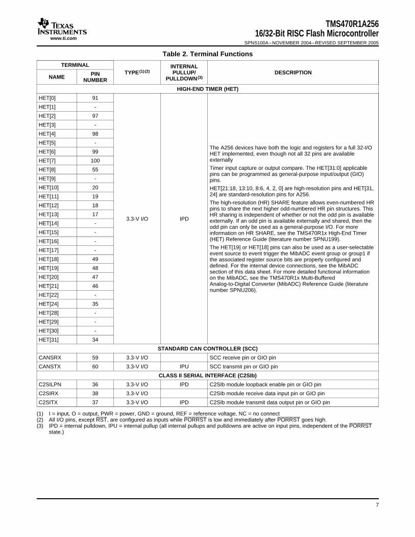
Table 2. Terminal Functions
TERMINAL INTERNALTYPE (1) (2) PULLUP/ DESCRIPTIONPINNAME PULLDOWN (3)NUMBER
HIGH-END TIMER (HET)
HET[0] 91
HET[1] -
HET[2] 97
HET[3] -
HET[4] 98
HET[5] -The A256 devices have both the logic and registers for a full 32-I/O
HET[6] 99 HET implemented, even though not all 32 pins are availableexternallyHET[7] 100Timer input capture or output compare. The HET[31:0] applicableHET[8] 55pins can be programmed as general-purpose input/output (GIO)
HET[9] - pins.HET[10] 20 HET[21:18, 13:10, 8:6, 4, 2, 0] are high-resolution pins and HET[31,
24] are standard-resolution pins for A256.HET[11] 19The high-resolution (HR) SHARE feature allows even-numbered HRHET[12] 18pins to share the next higher odd-numbered HR pin structures. This
HET[13] 17 HR sharing is independent of whether or not the odd pin is available3.3-V I/O IPD externally. If an odd pin is available externally and shared, then theHET[14] -
odd pin can only be used as a general-purpose I/O. For moreHET[15] - information on HR SHARE, see the TMS470R1x High-End Timer
(HET) Reference Guide (literature number SPNU199).HET[16] -The HET[19] or HET[18] pins can also be used as a user-selectableHET[17] -event source to event trigger the MibADC event group or group1 if
HET[18] 49 the associated register source bits are properly configured anddefined. For the internal device connections, see the MibADCHET[19] 48section of this data sheet. For more detailed functional information
HET[20] 47 on the MibADC, see the TMS470R1x Multi-BufferedAnalog-to-Digital Converter (MibADC) Reference Guide (literatureHET[21] 46number SPNU206).
HET[22] -
HET[24] 35
HET[28] -
HET[29] -
HET[30] -
HET[31] 34
STANDARD CAN CONTROLLER (SCC)
CANSRX 59 3.3-V I/O SCC receive pin or GIO pin
CANSTX 60 3.3-V I/O IPU SCC transmit pin or GIO pin
CLASS II SERIAL INTERFACE (C2SIb)
C2SILPN 36 3.3-V I/O IPD C2SIb module loopback enable pin or GIO pin
C2SIRX 38 3.3-V I/O C2SIb module receive data input pin or GIO pin
C2SITX 37 3.3-V I/O IPD C2SIb module transmit data output pin or GIO pin
(1) I = input, O = output, PWR = power, GND = ground, REF = reference voltage, NC = no connect(2) All I/O pins, except RST, are configured as inputs while PORRST is low and immediately after PORRST goes high.(3) IPD = internal pulldown, IPU = internal pullup (all internal pullups and pulldowns are active on input pins, independent of the PORRST
state.)
7
www.ti.com
TMS470R1A25616/32-Bit RISC Flash MicrocontrollerSPNS100A–NOVEMBER 2004–REVISED SEPTEMBER 2005
Table 2. Terminal Functions (continued)
TERMINAL INTERNALTYPE (1) (2) PULLUP/ DESCRIPTIONPINNAME PULLDOWN (3)NUMBER
GENERAL-PURPOSE I/O (GIO)
GIOA[0]/INT0 28 3.3-V I
GIOA[1]/INT1/ 29ECLK
GIOA[2]/INT2 30
GIOA[3]/INT3 31General-purpose input/output pins.GIOA[4]/INT4 25GIOA[0]/INT[0] is an input-only pin. GIOA[7:0]/INT[7:0] are inter-GIOA[5]/INT5 24rupt-capable pins.
GIOA[6]/INT6 23 GIOA[1]/INT[1]/ECLK pin is multiplexed with the external clock-outGIOA[7]/INT7 22 3.3-V I/O IPD function of the external clock prescale (ECP) module.
GIOB[0] 16
GIOB[1] 15
GIOB[2] 14
GIOB[3] 13
MULTI-BUFFERED ANALOG-TO-DIGITAL CONVERTER (MibADC)
MibADC event input. ADEVT can be programmed as a GIO pin.TheADEVT pin can also be used as a user-selectable event source toevent trigger the MibADC event group or group1 if the associatedADEVT 66 3.3-V I/O register source bits are properly configured and defined. For theinternal device connections, see the MibADC section of this datasheet.
ADIN[0] 75
ADIN[1] 74
ADIN[2] 73
ADIN[3] 72
ADIN[4] 71
ADIN[5] 69 IPDADIN[6] 68
ADIN[7] 673.3-V I MibADC analog input pins
ADIN[8] 82
ADIN[9] 80
ADIN[10] 78
ADIN[11] 76
ADIN[12] 81
ADIN[13] 79
ADIN[14] 77
ADIN[15] 70
ADREFHI 83 3.3-V REF I MibADC module high-voltage reference input
ADREFLO 84 GND REF I MibADC module low-voltage reference input
VCCAD 85 3.3-V PWR MibADC analog supply voltage
VSSAD 86 GND MibADC analog ground reference.
8
www.ti.com
TMS470R1A25616/32-Bit RISC Flash Microcontroller
SPNS100A–NOVEMBER 2004–REVISED SEPTEMBER 2005
Table 2. Terminal Functions (continued)
TERMINAL INTERNALTYPE (1) (2) PULLUP/ DESCRIPTIONPINNAME PULLDOWN (3)NUMBER
SERIAL PERIPHERAL INTERFACE 1 (SPI1)
SPI1CLK 5 SPI1 clock. SPI1CLK can be programmed as a GIO pin.
SPI1ENA 1 SPI1 chip enable. SPI1ENA can be programmed as a GIO pin.
SPI1SCS 2 SPI1 slave chip select. SPI1SCS can be programmed as a GIO pin.3.3-V I/O IPD SPI1 data stream. Slave in/master out. SPI1SIMO can be pro-SPI1SIMO 3 grammed as a GIO pin.
SPI1 data stream. Slave out/master in. SPI1SOMI can be pro-SPI1SOMI 4 grammed as a GIO pin.
SERIAL PERIPHERAL INTERFACE 2 (SPI2)
SPI2CLK 41 SPI2 clock. SPI2CLK can be programmed as a GIO pin.
SPI2ENA 44 SPI2 chip enable. SPI2ENA can be programmed as a GIO pin.
SPI2SCS 45 SPI2 slave chip select. SPI2SCS can be programmed as a GIO pin.3.3-V I/O IPD SPI2 data stream. Slave in/master out. SPI2SIMO can be pro-SPI2SIMO 42 grammed as a GIO pin.
SPI2 data stream. Slave out/master in. SPI2SOMI can be pro-SPI2SOMI 43 grammed as a GIO pin.
ZERO-PIN PHASE-LOCKED LOOP (ZPLL)
OSCIN 8 1.8-V I Crystal connection pin or external clock input
OSCOUT 7 1.8-V O External crystal connection pin
Enable/disable the ZPLL. The ZPLL can be bypassed and theoscillator becomes the system clock. If not in bypass mode, TIPLLDIS 51 3.3-V I IPD recommends that PLLDIS be connected to ground or pulled down toground by an external resistor.
SERIAL COMMUNICATIONS INTERFACE 1 (SCI1)
SCI1CLK 61 3.3-V I/O IPD SCI1 clock. SCI1CLK can be programmed as a GIO pin.
SCI1RX 63 3.3-V I/O IPU SCI1 data receive. SCI1RX can be programmed as a GIO pin.
SCI1TX 62 3.3-V I/O IPU SCI1 data transmit. SCI1TX can be programmed as a GIO pin.
SERIAL COMMUNICATIONS INTERFACE 2 (SCI2)
SCI2RX 32 3.3-V I/O IPU SCI2 data receive. SCI2RX can be programmed as a GIO pin.
SCI2TX 33 3.3-V I/O IPU SCI2 data transmit. SCI2TX can be programmed as a GIO pin.
SYSTEM MODULE (SYS)
Bidirectional pin. CLKOUT can be programmed as a GIO pin or theCLKOUT 58 3.3-V I/O IPD output of SYSCLK, ICLK, or MCLK.
Input master chip power-up reset. External VCC monitor circuitryPORRST 21 3.3-V I IPD must assert a power-on reset.
Bidirectional reset. The internal circuitry can assert a reset, and anexternal system reset can assert a device reset. On RST, the output
RST 10 3.3-V I/O IPU buffer is implemented as an open drain (drives low only). To ensurean external reset is not arbitrarily generated, TI recommends that anexternal pullup resistor be connected to RST.
WATCHDOG/REAL-TIME INTERRUPT (WD/RTI)
Analog watchdog reset. The AWD pin provides a system reset if theWD KEY is not written in time by the system, providing an externalRC network circuit is connected. If the user is not using AWD, TIrecommends that AWD be connected to ground or pulled down toground by an external resistor.
AWD 50 3.3-V I/O IPDFor more details on the external RC network circuit, see theTMS470R1x System Module Reference Guide(literature numberSPNU189) and the application note Analog Watchdog Resistor,Capacitor and Discharge Interval Selection Constraints (literaturenumber SPNA005).
9
www.ti.com
TMS470R1A25616/32-Bit RISC Flash MicrocontrollerSPNS100A–NOVEMBER 2004–REVISED SEPTEMBER 2005
Table 2. Terminal Functions (continued)
TERMINAL INTERNALTYPE (1) (2) PULLUP/ DESCRIPTIONPINNAME PULLDOWN (3)NUMBER
TEST/DEBUG (T/D)
TCK 54 3.3-V I IPD Test clock. TCK controls the test hardware (JTAG)
Test data in. TDI inputs serial data to the test instruction register,TDI 52 3.3-V I IPU test data register, and programmable test address (JTAG).
Test data out. TDO outputs serial data from the test instructionTDO 53 3.3-V O IPD register, test data register, identification register, and programmable
test address (JTAG).
Test enable. Reserved for internal use only. TI recommends thatTEST 27 3.3-V I IPD TEST be connected to ground or pulled down to ground by an
external resistor.
Serial input for controlling the state of the CPU test access portTMS 87 3.3-V I IPU (TAP) controller (JTAG)
Serial input for controlling the second TAP. TI recommends thatTMS2 88 3.3-V I IPU TMS2 be connected to VCCIO or pulled up to VCCIO by an external
resistor.
Test hardware reset to TAP1 and TAP2. IEEE Standard 1149-1TRST 26 3.3-V I IPD (JTAG) Boundary-Scan Logic. TI recommends that TRST be pulled
down to ground by an external resistor.
FLASH
FLTP1 95 Flash test pads 1 and 2. For proper operation, these pins mustNC not be connected (no connect [NC]).FLTP2 94
VCCP 96 3.3-V PWR Flash external pump voltage (3.3 V)
SUPPLY VOLTAGE CORE (1.8 V)
9
40
VCC 65 1.8-V PWR Core logic supply voltage
90
93
SUPPLY VOLTAGE DIGITAL I/O (3.3 V)
12VCCIO 3.3-V PWR Digital I/O supply voltage
57
SUPPLY GROUND CORE
6
39
VSS 64 GND Core supply ground reference
89
92
SUPPLY GROUND DIGITAL I/O
11VSSIO GND Digital I/O supply ground reference
56
10
www.ti.com
A256 DEVICE-SPECIFIC INFORMATION
Memory
0xFFE8_C000
0xFFE8_8000
0xFFFF_FFFF
System Module Control Registers(512K Bytes)
Exception, Interrupt, andReset Vectors
Memory (4G Bytes)
Programand
Data Area
Peripheral Control Registers(512K Bytes)
Reserved
MPU Control Registers
Reserved
0xFFF8_00000xFFF7_FFFF
0xFFF0_0000
0xFFE8_BFFF
0xFFE8_7FFF
0xFFE8_40240xFFE8_40230xFFE8_4000
0xFFE0_0000
0x0000_001F
0x0000_0000
FIQ
IRQ
Reserved
Data Abort
Prefetch Abort
Software Interrupt
Undefined Instruction
Reset
0x0000_ 001F
0x0000_ 001C
0x0000_ 0018
0x0000_ 0014
0x0000_ 0010
0x0000_ 000C
0x0000_ 0008
0x0000_ 0004
0x0000_ 0000
Reserved
0xFFFF_FD00
0xFFF8_0000
HET0xFFF7_FC00
0xFFF7_F800
0xFFF7_F400
0xFFF7_F000
0xFFF7_EC00
0xFFF7_E400
SPI1
SCI1
MibADC
GIO/ECP
Reserved
RAM(12K Bytes)
FLASH(256K Bytes)14 Sectors
Flash Control Registers
Reserved0xFFEF_FFFF
SCC RAM
SCC0xFFF7_E000
0xFFF7_DC00
0xFFF7_D800
0xFFF7_D400
C2SIb
Reserved0xFFF0_0000
SYSTEM
0xFFE8_3FFF
SCI20xFFF7_F500
Reserved
RESERVED
SPI2
0xFFF7_C800
0xFFF7_CC00
0xFFFF_FFFF
0x0000_0020
HET RAM(1K Byte)
TMS470R1A25616/32-Bit RISC Flash Microcontroller
SPNS100A–NOVEMBER 2004–REVISED SEPTEMBER 2005
Figure 1 shows the memory map of the A256 device.
A. Memory addresses are configurable by the system (SYS) module within the range of 0x0000_0000 to 0xFFE0_0000.
B. The CPU registers are not part of the memory map.
Figure 1. Memory Map
11
www.ti.com
Memory Selects
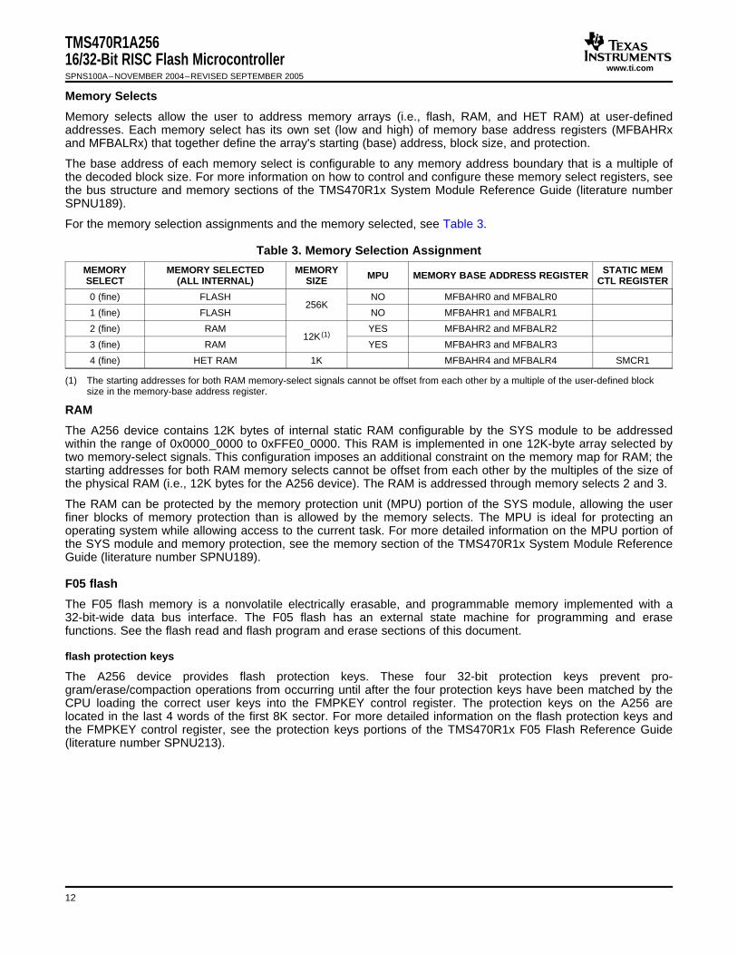
TMS470R1A25616/32-Bit RISC Flash MicrocontrollerSPNS100A–NOVEMBER 2004–REVISED SEPTEMBER 2005
Memory selects allow the user to address memory arrays (i.e., flash, RAM, and HET RAM) at user-definedaddresses. Each memory select has its own set (low and high) of memory base address registers (MFBAHRxand MFBALRx) that together define the array's starting (base) address, block size, and protection.
The base address of each memory select is configurable to any memory address boundary that is a multiple ofthe decoded block size. For more information on how to control and configure these memory select registers, seethe bus structure and memory sections of the TMS470R1x System Module Reference Guide (literature numberSPNU189).
For the memory selection assignments and the memory selected, see Table 3.
Table 3. Memory Selection Assignment
MEMORY MEMORY SELECTED MEMORY STATIC MEMMPU MEMORY BASE ADDRESS REGISTERSELECT (ALL INTERNAL) SIZE CTL REGISTER
0 (fine) FLASH NO MFBAHR0 and MFBALR0256K
1 (fine) FLASH NO MFBAHR1 and MFBALR1
2 (fine) RAM YES MFBAHR2 and MFBALR212K (1)
3 (fine) RAM YES MFBAHR3 and MFBALR3
4 (fine) HET RAM 1K MFBAHR4 and MFBALR4 SMCR1
(1) The starting addresses for both RAM memory-select signals cannot be offset from each other by a multiple of the user-defined blocksize in the memory-base address register.
RAM
The A256 device contains 12K bytes of internal static RAM configurable by the SYS module to be addressedwithin the range of 0x0000_0000 to 0xFFE0_0000. This RAM is implemented in one 12K-byte array selected bytwo memory-select signals. This configuration imposes an additional constraint on the memory map for RAM; thestarting addresses for both RAM memory selects cannot be offset from each other by the multiples of the size ofthe physical RAM (i.e., 12K bytes for the A256 device). The RAM is addressed through memory selects 2 and 3.
The RAM can be protected by the memory protection unit (MPU) portion of the SYS module, allowing the userfiner blocks of memory protection than is allowed by the memory selects. The MPU is ideal for protecting anoperating system while allowing access to the current task. For more detailed information on the MPU portion ofthe SYS module and memory protection, see the memory section of the TMS470R1x System Module ReferenceGuide (literature number SPNU189).
F05 flash
The F05 flash memory is a nonvolatile electrically erasable, and programmable memory implemented with a32-bit-wide data bus interface. The F05 flash has an external state machine for programming and erasefunctions. See the flash read and flash program and erase sections of this document.
flash protection keys
The A256 device provides flash protection keys. These four 32-bit protection keys prevent pro-gram/erase/compaction operations from occurring until after the four protection keys have been matched by theCPU loading the correct user keys into the FMPKEY control register. The protection keys on the A256 arelocated in the last 4 words of the first 8K sector. For more detailed information on the flash protection keys andthe FMPKEY control register, see the protection keys portions of the TMS470R1x F05 Flash Reference Guide(literature number SPNU213).
12
www.ti.com
TMS470R1A25616/32-Bit RISC Flash Microcontroller
SPNS100A–NOVEMBER 2004–REVISED SEPTEMBER 2005
flash read
The A256 flash memory is configurable by the SYS module to be addressed within the range of 0x0000_0000 to0xFFE0_0000. The flash is addressed through memory selects 0 and 1.
NOTE:
The flash external pump voltage (VCCP) is required for all operations (program, erase,and read).
flash pipeline mode
When in pipeline mode, the flash operates with a system clock frequency of up to 48 MHz. In normal mode, itoperates with a system clock frequency of up to 24 MHz. Flash in pipeline mode is capable of accessing 64-bitwords and provides two 32-bit pipelined words to the CPU. Also in pipeline mode, the flash can be read with nowait states when memory addresses are contiguous (after the initial 1-or 2-wait-state reads).
NOTE:
After a system reset, pipeline mode is disabled (ENPIPE bit FMREGOPT[0] = 0). Inother words, the A256 device powers up and comes out of reset in non-pipelinemode. Furthermore, setting the flash configuration mode bit (GLBCTRL[4]) willoverride pipeline mode.
flash program and erase
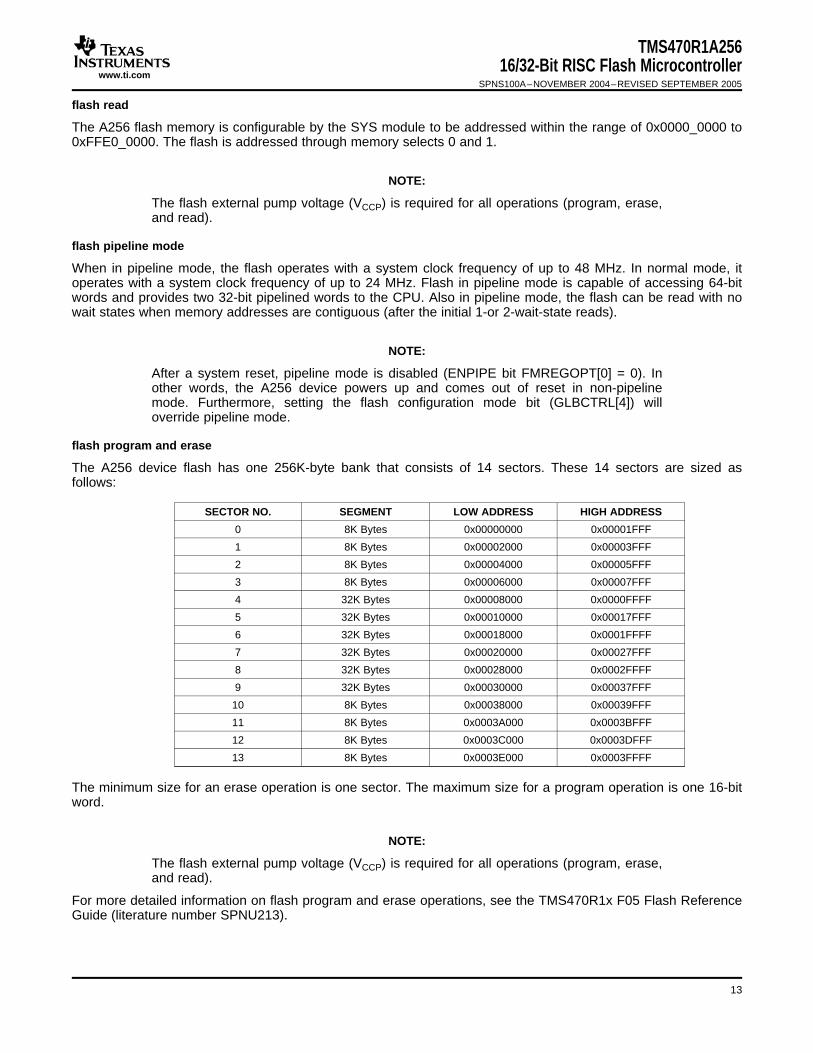
The A256 device flash has one 256K-byte bank that consists of 14 sectors. These 14 sectors are sized asfollows:
SECTOR NO. SEGMENT LOW ADDRESS HIGH ADDRESS
0 8K Bytes 0x00000000 0x00001FFF
1 8K Bytes 0x00002000 0x00003FFF
2 8K Bytes 0x00004000 0x00005FFF
3 8K Bytes 0x00006000 0x00007FFF
4 32K Bytes 0x00008000 0x0000FFFF
5 32K Bytes 0x00010000 0x00017FFF
6 32K Bytes 0x00018000 0x0001FFFF
7 32K Bytes 0x00020000 0x00027FFF
8 32K Bytes 0x00028000 0x0002FFFF
9 32K Bytes 0x00030000 0x00037FFF
10 8K Bytes 0x00038000 0x00039FFF
11 8K Bytes 0x0003A000 0x0003BFFF
12 8K Bytes 0x0003C000 0x0003DFFF
13 8K Bytes 0x0003E000 0x0003FFFF
The minimum size for an erase operation is one sector. The maximum size for a program operation is one 16-bitword.
NOTE:
The flash external pump voltage (VCCP) is required for all operations (program, erase,and read).
For more detailed information on flash program and erase operations, see the TMS470R1x F05 Flash ReferenceGuide (literature number SPNU213).
13
www.ti.com
Peripheral Selects and Base Addresses
TMS470R1A25616/32-Bit RISC Flash MicrocontrollerSPNS100A–NOVEMBER 2004–REVISED SEPTEMBER 2005
HET RAM
The A256 device contains HET RAM. The HET RAM has a 64-instruction capability. The HET RAM isconfigurable by the SYS module to be addressed within the range of 0x0000_0000 to 0xFFE0_0000. The HETRAM is addressed through memory select 4.
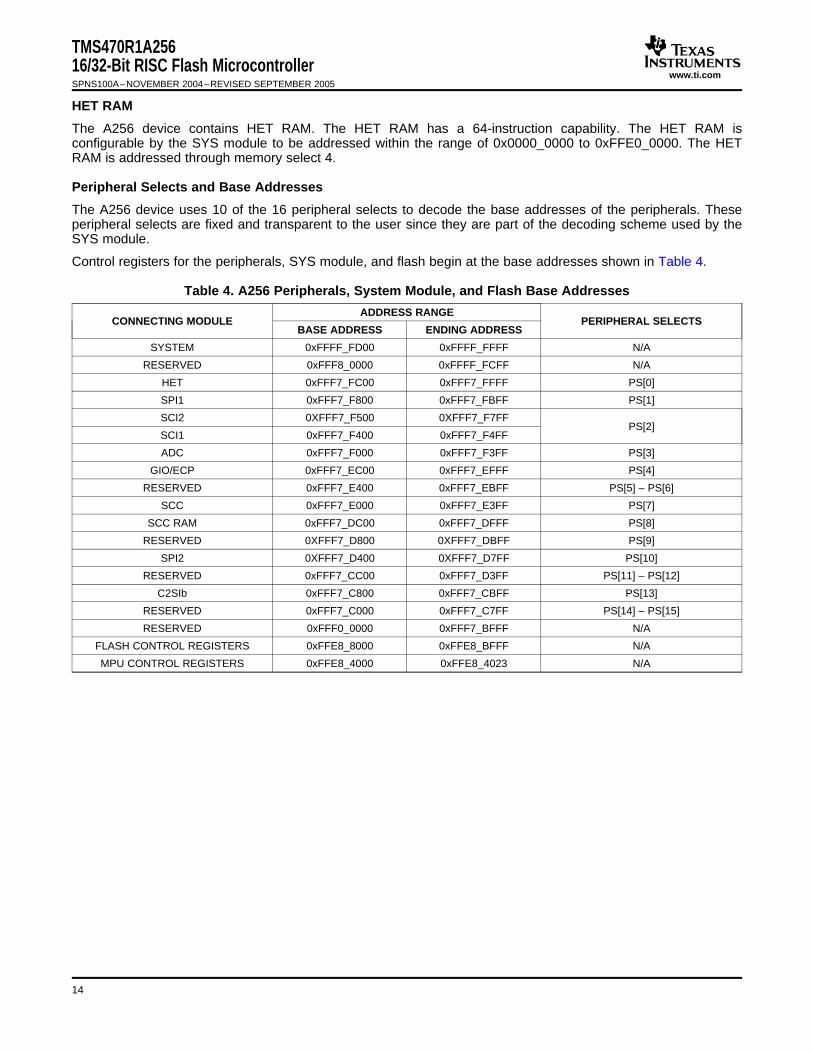
The A256 device uses 10 of the 16 peripheral selects to decode the base addresses of the peripherals. Theseperipheral selects are fixed and transparent to the user since they are part of the decoding scheme used by theSYS module.
Control registers for the peripherals, SYS module, and flash begin at the base addresses shown in Table 4.
Table 4. A256 Peripherals, System Module, and Flash Base Addresses
ADDRESS RANGECONNECTING MODULE PERIPHERAL SELECTS
BASE ADDRESS ENDING ADDRESS
SYSTEM 0xFFFF_FD00 0xFFFF_FFFF N/A
RESERVED 0xFFF8_0000 0xFFFF_FCFF N/A
HET 0xFFF7_FC00 0xFFF7_FFFF PS[0]
SPI1 0xFFF7_F800 0xFFF7_FBFF PS[1]
SCI2 0XFFF7_F500 0XFFF7_F7FFPS[2]
SCI1 0xFFF7_F400 0xFFF7_F4FF
ADC 0xFFF7_F000 0xFFF7_F3FF PS[3]
GIO/ECP 0xFFF7_EC00 0xFFF7_EFFF PS[4]
RESERVED 0xFFF7_E400 0xFFF7_EBFF PS[5] – PS[6]
SCC 0xFFF7_E000 0xFFF7_E3FF PS[7]
SCC RAM 0xFFF7_DC00 0xFFF7_DFFF PS[8]
RESERVED 0XFFF7_D800 0XFFF7_DBFF PS[9]
SPI2 0XFFF7_D400 0XFFF7_D7FF PS[10]
RESERVED 0xFFF7_CC00 0xFFF7_D3FF PS[11] – PS[12]
C2SIb 0xFFF7_C800 0xFFF7_CBFF PS[13]
RESERVED 0xFFF7_C000 0xFFF7_C7FF PS[14] – PS[15]
RESERVED 0xFFF0_0000 0xFFF7_BFFF N/A
FLASH CONTROL REGISTERS 0xFFE8_8000 0xFFE8_BFFF N/A
MPU CONTROL REGISTERS 0xFFE8_4000 0xFFE8_4023 N/A
14

www.ti.com
Interrupt Priority
TMS470R1A25616/32-Bit RISC Flash Microcontroller
SPNS100A–NOVEMBER 2004–REVISED SEPTEMBER 2005
The central interrupt manager (CIM) portion of the SYS module manages the interrupt requests from the devicemodules (i.e., SPI1 or SPI2, SCI1 or SCI2, and RTI, etc.).
Although the CIM can accept up to 32 interrupt request signals, the A256 device only uses 21 of those interruptrequest signals. The request channels are maskable so that individual channels can be selectively disabled. Allinterrupt requests can be programmed in the CIM to be of either type:• Fast interrupt request (FIQ)• Normal interrupt request (IRQ)
The precedences of request channels decrease with ascending channel order in the CIM (0 [highest] and 31[lowest] priority). For these channel priorities and the associated modules, see Table 5.
Table 5. Interrupt Priority
MODULES INTERRUPT SOURCES INTERRUPT LEVEL/CHANNEL
SPI1 SPI1 end-transfer/overrun 0
RTI COMP2 interrupt 1
RTI COMP1 interrupt 2
RTI TAP interrupt 3
SPI2 SPI2 end-transfer/overrun 4
GIO Interrupt A 5
RESERVED 6
HET Interrupt 1 7
RESERVED 8
SCI1/SCI2 SCI1/SCI2 error interrupt 9
SCI1 SCI1 receive interrupt 10
C2SIb C2SIb interrupt 11
RESERVED 12
RESERVED 13
SCC Interrupt A 14
RESERVED 15
MibADC End event conversion 16
SCI2 SCI2 receive interrupt 17
RESERVED 18
RESERVED 19
SCI1 SCI1 transmit interrupt 20
System SW interrupt (SSI) 21
RESERVED 22
HET Interrupt 2 23
RESERVED 24
SCC Interrupt B 25
SCI2 SCI2 transmit interrupt 26
MibADC End Group 1 conversion 27
RESERVED 28
GIO Interrupt B 29
MibADC End Group 2 conversion 30
RESERVED 31
15
www.ti.com
MibADC
TMS470R1A25616/32-Bit RISC Flash MicrocontrollerSPNS100A–NOVEMBER 2004–REVISED SEPTEMBER 2005
The multi-buffered analog-to-digital converter (MibADC) accepts an analog signal and converts the signal to a10-bit digital value.
The A256 MibADC module can function in two modes: compatibility mode, where its programmer's model iscompatible with the TMS470R1x ADC module and its digital results are stored in digital result registers; or inbuffered mode, where the digital result registers are replaced with three FIFO buffers, one for each conversiongroup (event, group1 [G1], and group2 [G2]). In buffered mode, the MibADC buffers can be serviced byinterrupts.
MibADC event trigger enhancements
The MibADC includes two major enhancements over the event-triggering capability of the TMS470R1x ADC.• Both group1 and the event group can be configured for event-triggered operation, providing up to two
event-triggered groups.• The trigger source and polarity can be selected individually for both group 1 and the event group from the
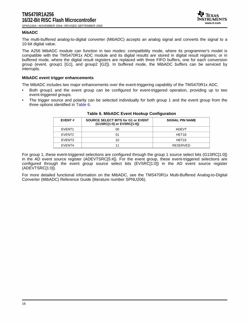
three options identified in Table 6.
Table 6. MibADC Event Hookup Configuration
EVENT # SOURCE SELECT BITS for G1 or EVENT SIGNAL PIN NAME(G1SRC[1:0] or EVSRC[1:0])
EVENT1 00 ADEVT
EVENT2 01 HET18
EVENT3 10 HET19
EVENT4 11 RESERVED
For group 1, these event-triggered selections are configured through the group 1 source select bits (G1SRC[1:0])in the AD event source register (ADEVTSRC[5:4]). For the event group, these event-triggered selections areconfigured through the event group source select bits (EVSRC[1:0]) in the AD event source register(ADEVTSRC[1:0]).
For more detailed functional information on the MibADC, see the TMS470R1x Multi-Buffered Analog-to-DigitalConverter (MibADC) Reference Guide (literature number SPNU206).
16
www.ti.com
Documentation Support
TMS470R1A25616/32-Bit RISC Flash Microcontroller
SPNS100A–NOVEMBER 2004–REVISED SEPTEMBER 2005
Extensive documentation supports all of the TMS470 microcontroller family generation of devices. The types ofdocumentation available include: data sheets with design specifications; complete user's guides; and erratasheets. Useful reference documentation includes:• Bulletin
– TMS470 Microcontroller Family Product Bulletin (literature number SPNB086)• User's Guides
– TMS470R1x System Module Reference Guide (literature number SPNU189)– TMS470R1x General Purpose Input/Output (GIO) Reference Guide (literature number SPNU192)– TMS470R1x Direct Memory Access (DMA) Controller Reference Guide (literature number SPNU194)– TMS470R1x Serial Peripheral Interface (SPI) Reference Guide (literature number SPNU195)– TMS470R1x Serial Communication Interface (SCI) Reference Guide (literature number SPNU196)– TMS470R1x Controller Area Network (CAN) Reference Guide (literature number SPNU197)– TMS470R1x High End Timer (HET) Reference Guide (literature number SPNU199)– TMS470R1x External Clock Prescale (ECP) Reference Guide (literature number SPNU202)– TMS470R1x MultiBuffered Analog to Digital (MibADC) Reference Guide (literature number SPNU206)– TMS470R1x ZeroPin Phase Locked Loop (ZPLL) Clock Module Reference Guide (literature number
SPNU212)– TMS470R1x F05 Flash Reference Guide (literature number SPNU213)– TMS470R1x Class II Serial Interface B (C2SIb) Reference Guide (literature number SPNU214)– TMS470R1x Class II Serial Interface A (C2SIa) Reference Guide (literature number SPNU218)– TMS470R1x Inter-Integrated Circuit (I2C) Reference Guide (literature number SPNU223)– TMS470 Peripherals Overview Reference Guide (literature number SPNU248)
• Errata Sheet:– TMS470R1A256 TMS470 Microcontrollers Silicon Errata (literature number SPNZ133)
17
www.ti.com
Device and Development-Support Tool Nomenclature
TMS470R1A25616/32-Bit RISC Flash MicrocontrollerSPNS100A–NOVEMBER 2004–REVISED SEPTEMBER 2005
To designate the stages in the product development cycle, TI assigns prefixes to the part numbers of all DSPdevices and support tools. Each DSP commercial family member has one of three prefixes: TMX, TMP, or TMS(e.g., TMS470R1A256). Texas Instruments recommends two of three possible prefix designators for its supporttools: TMDX and TMDS. These prefixes represent evolutionary stages of product development from engineeringprototypes (TMX/TMDX) through fully qualified production devices/tools (TMS/TMDS).
Device development evolutionary flow:
TMX Experimental device that is not necessarily representative of the final device's electrical specifi-cations
TMP Final silicon die that conforms to the device's electrical specifications but has not completed qualityand reliability verification
TMS Fully qualified production device
Support tool development evolutionary flow:
TMDX Development-support product that has not yet completed Texas Instruments internal qualificationtesting.
TMDS Fully qualified development-support product
TMX and TMP devices and TMDX development-support tools are shipped against the following disclaimer:
"Developmental product is intended for internal evaluation purposes."
TMS devices and TMDS development-support tools have been characterized fully, and the quality and reliabilityof the device have been demonstrated fully. TI's standard warranty applies.
Predictions show that prototype devices (TMX or TMP) have a greater failure rate than the standard productiondevices. Texas Instruments recommends that these devices not be used in any production system because theirexpected end-use failure rate still is undefined. Only qualified production devices are to be used.
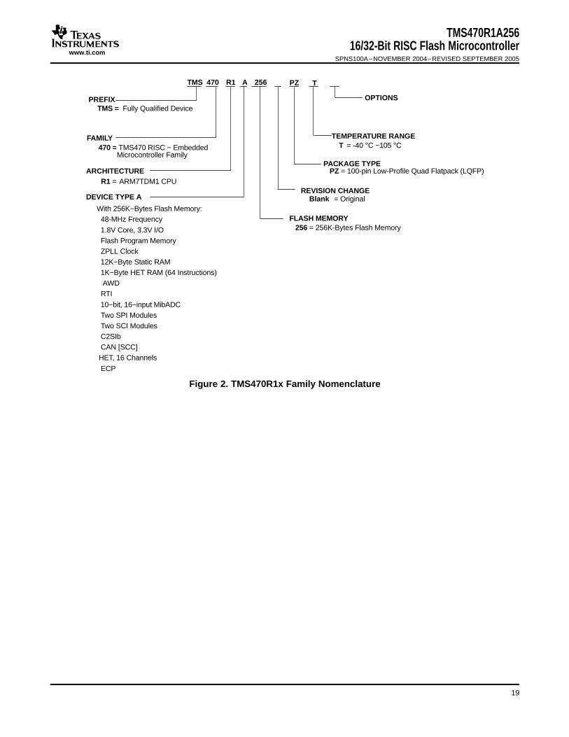
Figure 2 illustrates the numbering and symbol nomenclature for the TMS470R1x family.
18
www.ti.com
PREFIX
470
FAMILY
DEVICE TYPE A
PZ = 100-pin Low-Profile Quad Flatpack (LQFP)
TMS
470 = TMS470 RISC − Embedded Microcontroller Family
A
PACKAGE TYPE
R1
ARCHITECTURER1 = ARM7TDM1 CPU
TMS = Fully Qualified Device
256 = 256K-Bytes Flash Memory
256
REVISION CHANGEBlank = Original
OPTIONS
FLASH MEMORYWith 256K−Bytes Flash Memory: 48-MHz Frequency
1.8V Core, 3.3V I/O Flash Program Memory ZPLL Clock 12K−Byte Static RAM 1K−Byte HET RAM (64 Instructions) AWD RTI
10−bit, 16−input MibADC Two SPI Modules Two SCI Modules C2SIb CAN [SCC] HET, 16 Channels
ECP
PZ
TEMPERATURE RANGET = -40 °C −105 °C
T
TMS470R1A25616/32-Bit RISC Flash Microcontroller
SPNS100A–NOVEMBER 2004–REVISED SEPTEMBER 2005
Figure 2. TMS470R1x Family Nomenclature
19
www.ti.com
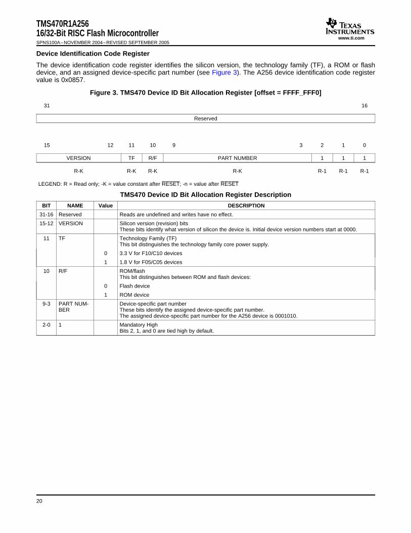
Device Identification Code Register
TMS470R1A25616/32-Bit RISC Flash MicrocontrollerSPNS100A–NOVEMBER 2004–REVISED SEPTEMBER 2005
The device identification code register identifies the silicon version, the technology family (TF), a ROM or flashdevice, and an assigned device-specific part number (see Figure 3). The A256 device identification code registervalue is 0x0857.
Figure 3. TMS470 Device ID Bit Allocation Register [offset = FFFF_FFF0]
31 16
Reserved
15 12 11 10 9 3 2 1 0
VERSION TF R/F PART NUMBER 1 1 1
R-K R-K R-K R-K R-1 R-1 R-1
LEGEND: R = Read only; -K = value constant after RESET; -n = value after RESET
TMS470 Device ID Bit Allocation Register Description
BIT NAME Value DESCRIPTION
31-16 Reserved Reads are undefined and writes have no effect.
15-12 VERSION Silicon version (revision) bitsThese bits identify what version of silicon the device is. Initial device version numbers start at 0000.
11 TF Technology Family (TF)This bit distinguishes the technology family core power supply.
0 3.3 V for F10/C10 devices
1 1.8 V for F05/C05 devices
10 R/F ROM/flashThis bit distinguishes between ROM and flash devices:
0 Flash device
1 ROM device
9-3 PART NUM- Device-specific part numberBER These bits identify the assigned device-specific part number.
The assigned device-specific part number for the A256 device is 0001010.
2-0 1 Mandatory HighBits 2, 1, and 0 are tied high by default.
20
www.ti.com
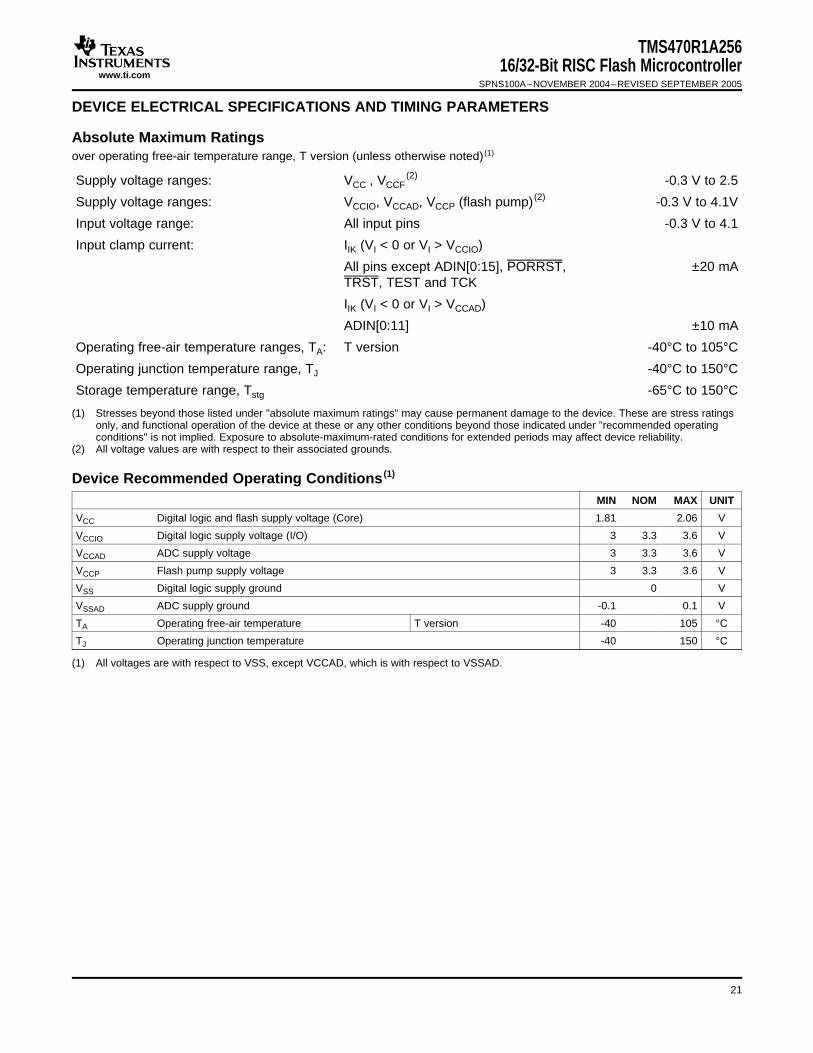
DEVICE ELECTRICAL SPECIFICATIONS AND TIMING PARAMETERS
Absolute Maximum Ratings
Device Recommended Operating Conditions (1)
TMS470R1A25616/32-Bit RISC Flash Microcontroller
SPNS100A–NOVEMBER 2004–REVISED SEPTEMBER 2005
over operating free-air temperature range, T version (unless otherwise noted) (1)
Supply voltage ranges: VCC , VCCF(2) -0.3 V to 2.5
Supply voltage ranges: VCCIO, VCCAD, VCCP (flash pump) (2) -0.3 V to 4.1V
Input voltage range: All input pins -0.3 V to 4.1
Input clamp current: IIK (VI < 0 or VI > VCCIO)
All pins except ADIN[0:15], PORRST, ±20 mATRST, TEST and TCK
IIK (VI < 0 or VI > VCCAD)
ADIN[0:11] ±10 mA
Operating free-air temperature ranges, TA: T version -40°C to 105°C
Operating junction temperature range, TJ -40°C to 150°C
Storage temperature range, Tstg -65°C to 150°C
(1) Stresses beyond those listed under "absolute maximum ratings" may cause permanent damage to the device. These are stress ratingsonly, and functional operation of the device at these or any other conditions beyond those indicated under "recommended operatingconditions" is not implied. Exposure to absolute-maximum-rated conditions for extended periods may affect device reliability.
(2) All voltage values are with respect to their associated grounds.
MIN NOM MAX UNIT
VCC Digital logic and flash supply voltage (Core) 1.81 2.06 V
VCCIO Digital logic supply voltage (I/O) 3 3.3 3.6 V
VCCAD ADC supply voltage 3 3.3 3.6 V
VCCP Flash pump supply voltage 3 3.3 3.6 V
VSS Digital logic supply ground 0 V
VSSAD ADC supply ground -0.1 0.1 V
TA Operating free-air temperature T version -40 105 °C
TJ Operating junction temperature -40 150 °C
(1) All voltages are with respect to VSS, except VCCAD, which is with respect to VSSAD.
21
www.ti.com
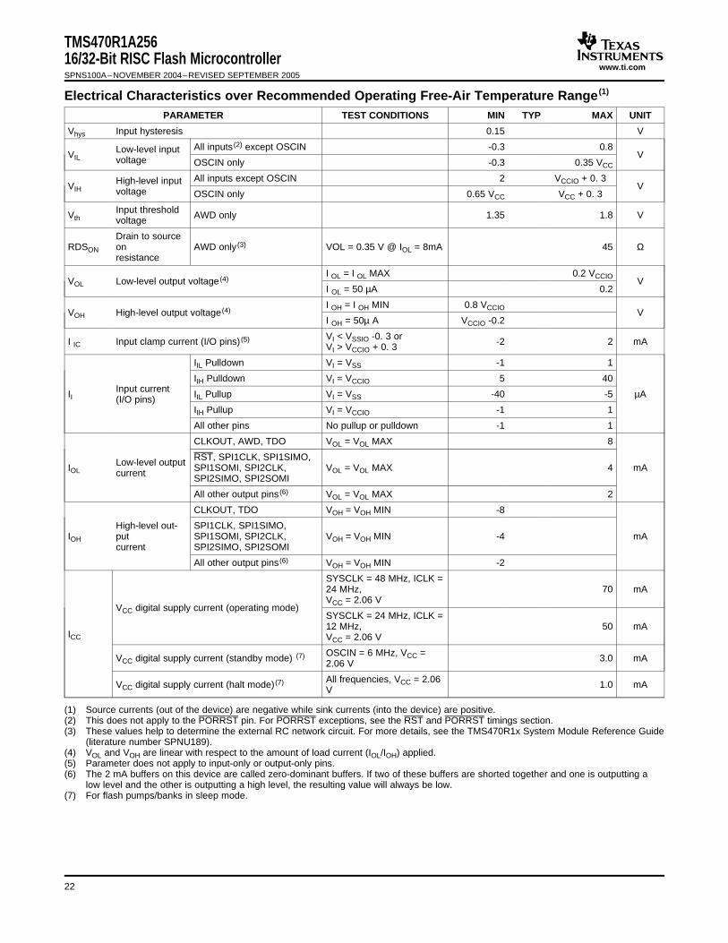
Electrical Characteristics over Recommended Operating Free-Air Temperature Range (1)
TMS470R1A25616/32-Bit RISC Flash MicrocontrollerSPNS100A–NOVEMBER 2004–REVISED SEPTEMBER 2005
PARAMETER TEST CONDITIONS MIN TYP MAX UNIT
Vhys Input hysteresis 0.15 V
All inputs (2) except OSCIN -0.3 0.8Low-level inputVIL Vvoltage OSCIN only -0.3 0.35 VCC
All inputs except OSCIN 2 VCCIO + 0. 3High-level inputVIH Vvoltage OSCIN only 0.65 VCC VCC + 0. 3
Input thresholdVth AWD only 1.35 1.8 Vvoltage
Drain to sourceRDSON on AWD only (3) VOL = 0.35 V @ IOL = 8mA 45 Ω
resistance
I OL = I OL MAX 0.2 VCCIOVOL Low-level output voltage (4) V
I OL = 50 µA 0.2
I OH = I OH MIN 0.8 VCCIOVOH High-level output voltage (4) V
I OH = 50µ A VCCIO -0.2
VI < VSSIO -0. 3 orI IC Input clamp current (I/O pins) (5) -2 2 mAVI > VCCIO + 0. 3
IIL Pulldown VI = VSS -1 1
IIH Pulldown VI = VCCIO 5 40Input currentII IIL Pullup VI = VSS -40 -5 µA(I/O pins)
IIH Pullup VI = VCCIO -1 1
All other pins No pullup or pulldown -1 1
CLKOUT, AWD, TDO VOL = VOL MAX 8
RST, SPI1CLK, SPI1SIMO,Low-level outputIOL SPI1SOMI, SPI2CLK, VOL = VOL MAX 4 mAcurrent SPI2SIMO, SPI2SOMI
All other output pins (6) VOL = VOL MAX 2
CLKOUT, TDO VOH = VOH MIN -8
High-level out- SPI1CLK, SPI1SIMO,IOH put SPI1SOMI, SPI2CLK, VOH = VOH MIN -4 mA
current SPI2SIMO, SPI2SOMI
All other output pins (6) VOH = VOH MIN -2
SYSCLK = 48 MHz, ICLK =24 MHz, 70 mAVCC = 2.06 V
VCC digital supply current (operating mode)SYSCLK = 24 MHz, ICLK =12 MHz, 50 mA
ICC VCC = 2.06 V
OSCIN = 6 MHz, VCC =VCC digital supply current (standby mode) (7) 3.0 mA2.06 V
All frequencies, VCC = 2.06VCC digital supply current (halt mode)(7) 1.0 mAV
(1) Source currents (out of the device) are negative while sink currents (into the device) are positive.(2) This does not apply to the PORRST pin. For PORRST exceptions, see the RST and PORRST timings section.(3) These values help to determine the external RC network circuit. For more details, see the TMS470R1x System Module Reference Guide
(literature number SPNU189).(4) VOL and VOH are linear with respect to the amount of load current (IOL/IOH) applied.(5) Parameter does not apply to input-only or output-only pins.(6) The 2 mA buffers on this device are called zero-dominant buffers. If two of these buffers are shorted together and one is outputting a
low level and the other is outputting a high level, the resulting value will always be low.(7) For flash pumps/banks in sleep mode.
22
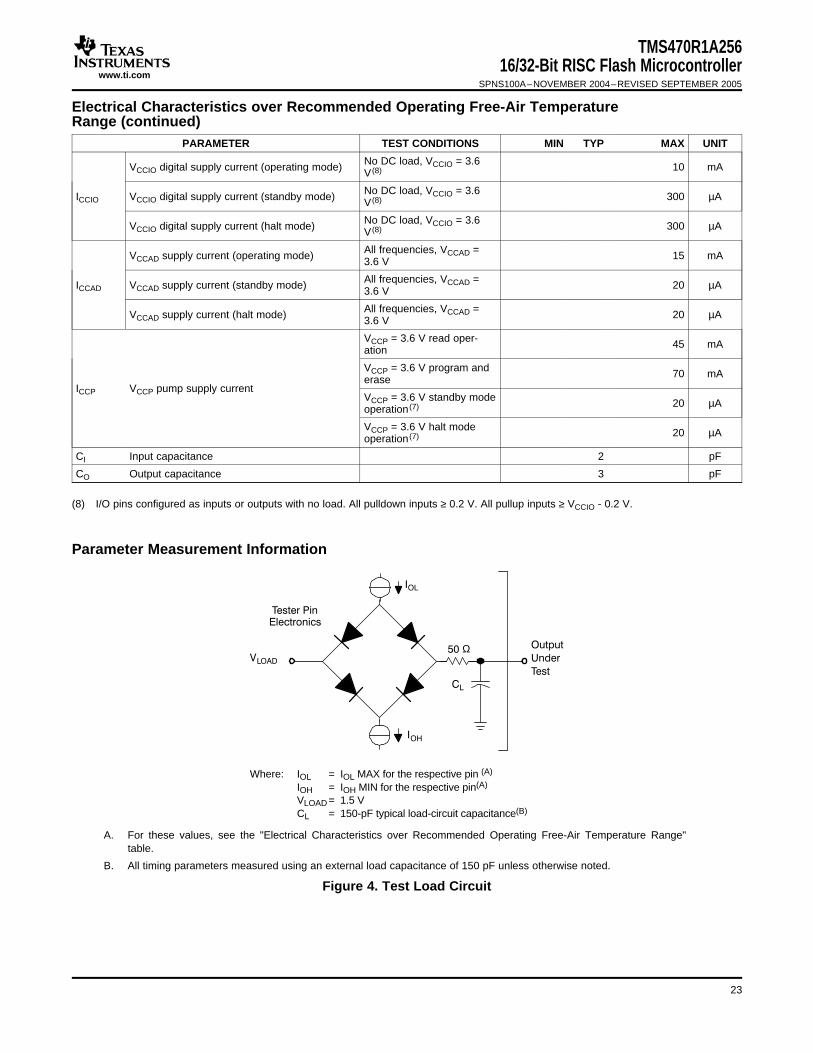
www.ti.com
Parameter Measurement Information
Ω
Where: IOL = IOL MAX for the respective pin (A)
IOH = IOH MIN for the respective pin(A)
VLOAD = 1.5 VCL = 150-pF typical load-circuit capacitance(B)
TMS470R1A25616/32-Bit RISC Flash Microcontroller
SPNS100A–NOVEMBER 2004–REVISED SEPTEMBER 2005
Electrical Characteristics over Recommended Operating Free-Air TemperatureRange (continued)
PARAMETER TEST CONDITIONS MIN TYP MAX UNIT
No DC load, VCCIO = 3.6VCCIO digital supply current (operating mode) 10 mAV (8)
No DC load, VCCIO = 3.6ICCIO VCCIO digital supply current (standby mode) 300 µAV (8)
No DC load, VCCIO = 3.6VCCIO digital supply current (halt mode) 300 µAV (8)
All frequencies, VCCAD =VCCAD supply current (operating mode) 15 mA3.6 V
All frequencies, VCCAD =ICCAD VCCAD supply current (standby mode) 20 µA3.6 V
All frequencies, VCCAD =VCCAD supply current (halt mode) 20 µA3.6 V
VCCP = 3.6 V read oper- 45 mAation
VCCP = 3.6 V program and 70 mAeraseICCP VCCP pump supply current
VCCP = 3.6 V standby mode 20 µAoperation (7)
VCCP = 3.6 V halt mode 20 µAoperation (7)
CI Input capacitance 2 pF
CO Output capacitance 3 pF
(8) I/O pins configured as inputs or outputs with no load. All pulldown inputs ≥ 0.2 V. All pullup inputs ≥ VCCIO - 0.2 V.
A. For these values, see the "Electrical Characteristics over Recommended Operating Free-Air Temperature Range"table.
B. All timing parameters measured using an external load capacitance of 150 pF unless otherwise noted.
Figure 4. Test Load Circuit
23
www.ti.com
Timing Parameter Symbology
TMS470R1A25616/32-Bit RISC Flash MicrocontrollerSPNS100A–NOVEMBER 2004–REVISED SEPTEMBER 2005
Timing parameter symbols have been created in accordance with JEDEC Standard 100. To shorten the symbols,some of the pin names and other related terminology have been abbreviated as follows:
CM Compaction, CMPCT RD Read
CO CLKOUT RST Reset, RST
ER Erase RX SCInRX
ICLK Interface clock S Slave mode
M Master mode SCC SCInCLK
OSC, OSCI OSCIN SIMO SPInSIMO
OSCO OSCOUT SOMI SPInSOMI
P Program, PROG SPC SPInCLK
R Ready SYS System clock
R0 Read margin 0, RDMRGN0 TX SCInTX
R1 Read margin 1, RDMRGN1
Lowercase subscripts and their meanings are:
a access time r rise time
c cycle time (period) su setup time
d delay time t transition time
f fall time v valid time
h hold time w pulse duration (width)
The following additional letters are used with these meanings:
H High X Unknown, changing, or don't care level
L Low Z High impedance
V Valid
24
www.ti.com
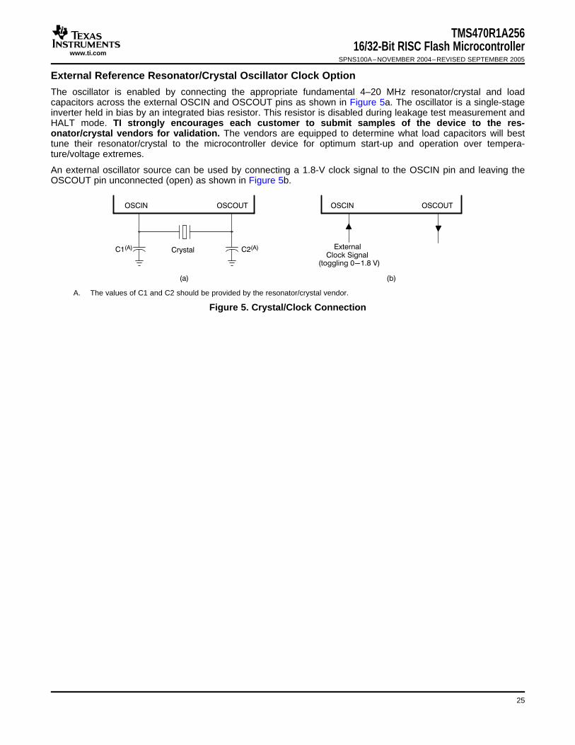
External Reference Resonator/Crystal Oscillator Clock Option
!
"
TMS470R1A25616/32-Bit RISC Flash Microcontroller
SPNS100A–NOVEMBER 2004–REVISED SEPTEMBER 2005
The oscillator is enabled by connecting the appropriate fundamental 4–20 MHz resonator/crystal and loadcapacitors across the external OSCIN and OSCOUT pins as shown in Figure 5a. The oscillator is a single-stageinverter held in bias by an integrated bias resistor. This resistor is disabled during leakage test measurement andHALT mode. TI strongly encourages each customer to submit samples of the device to the res-onator/crystal vendors for validation. The vendors are equipped to determine what load capacitors will besttune their resonator/crystal to the microcontroller device for optimum start-up and operation over tempera-ture/voltage extremes.
An external oscillator source can be used by connecting a 1.8-V clock signal to the OSCIN pin and leaving theOSCOUT pin unconnected (open) as shown in Figure 5b.
A. The values of C1 and C2 should be provided by the resonator/crystal vendor.
Figure 5. Crystal/Clock Connection
25
www.ti.com
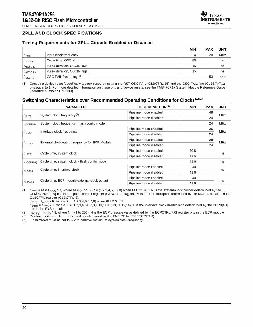
ZPLL AND CLOCK SPECIFICATIONS
Timing Requirements for ZPLL Circuits Enabled or Disabled
Switching Characteristics over Recommended Operating Conditions for Clocks (1) (2)
TMS470R1A25616/32-Bit RISC Flash MicrocontrollerSPNS100A–NOVEMBER 2004–REVISED SEPTEMBER 2005
MIN MAX UNIT
f(OSC) Input clock frequency 4 20 MHz
tc(OSC) Cycle time, OSCIN 50 ns
tw(OSCIL) Pulse duration, OSCIN low 15 ns
tw(OSCIH) Pulse duration, OSCIN high 15 ns
f(OSCRST) OSC FAIL frequency (1) 53 kHz
(1) Causes a device reset (specifically a clock reset) by setting the RST OSC FAIL (GLBCTRL.15) and the OSC FAIL flag (GLBSTAT.1)bits equal to 1. For more detailed information on these bits and device resets, see the TMS470R1x System Module Reference Guide(literature number SPNU189).
PARAMETER TEST CONDITION (3) MIN MAX UNIT
Pipeline mode enabled 48f(SYS) System clock frequency (4) MHz
Pipeline mode disabled 24
f(CONFIG) System clock frequency - flash config mode 24 MHz
Pipeline mode enabled 25f(ICLK) Interface clock frequency MHz
Pipeline mode disabled 24
Pipeline mode enabled 25f(ECLK) External clock output frequency for ECP Module MHz
Pipeline mode disabled 24
Pipeline mode enabled 20.8tc(SYS) Cycle time, system clock ns
Pipeline mode disabled 41.6
tc(CONFIG) Cycle time, system clock - flash config mode 41.6 ns
Pipeline mode enabled 40tc(ICLK) Cycle time, interface clock ns
Pipeline mode disabled 41.6
Pipeline mode enabled 40tc(ECLK) Cycle time, ECP module external clock output ns
Pipeline mode disabled 41.6
(1) f(SYS) = M × f(OSC) / R, where M = 4 or 8, R = 1,2,3,4,5,6,7,8 when PLLDIS = 0. R is the system-clock divider determined by theCLKDIVPRE [2:0] bits in the global control register (GLBCTRL[2:0]) and M is the PLL multiplier determined by the MULT4 bit, also in theGLBCTRL register (GLBCTRL.3).f(SYS) = f(OSC) / R, where R = 1,2,3,4,5,6,7,8 when PLLDIS = 1.f(ICLK) = f(SYS) / X, where X = 1,2,3,4,5,6,7,8,9,10,11,12,13,14,15,16. X is the interface clock divider ratio determined by the PCR0[4:1]bits in the SYS module.
(2) f(ECLK) = f(ICLK) / N, where N = 1 to 256. N is the ECP prescale value defined by the ECPCTRL[7:0] register bits in the ECP module(3) Pipeline mode enabled or disabled is determined by the ENPIPE bit (FMREGOPT.0).(4) Flash Vread must be set to 5 V to achieve maximum system clock frequency.
26
www.ti.com
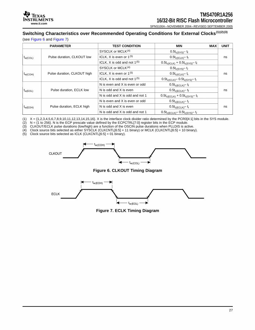
Switching Characteristics over Recommended Operating Conditions for External Clocks (1) (2) (3)
TMS470R1A25616/32-Bit RISC Flash Microcontroller
SPNS100A–NOVEMBER 2004–REVISED SEPTEMBER 2005
(see Figure 6 and Figure 7)
PARAMETER TEST CONDITION MIN MAX UNIT
SYSCLK or MCLK (4) 0.5tc(SYS)– tftw(COL) Pulse duration, CLKOUT low ICLK, X is even or 1 (5) 0.5tc(ICLK)– tf ns
ICLK, X is odd and not 1 (5) 0.5tc(ICLK) + 0.5tc(SYS)– tfSYSCLK or MCLK (4) 0.5tc(SYS)– tr
tw(COH) Pulse duration, CLKOUT high ICLK, X is even or 1 (5) 0.5tc(ICLK)– tr ns
ICLK, X is odd and not 1 (5) 0.5tc(ICLK)– 0.5tc(SYS)– trN is even and X is even or odd 0.5tc(ECLK)– tf
tw(EOL) Pulse duration, ECLK low N is odd and X is even 0.5tc(ECLK)– tf ns
N is odd and X is odd and not 1 0.5tc(ECLK) + 0.5tc(SYS)– tfN is even and X is even or odd 0.5tc(ECLK)– tr
tw(EOH) Pulse duration, ECLK high N is odd and X is even 0.5tc(ECLK)– tr ns
N is odd and X is odd and not 1 0.5tc(ECLK)– 0.5tc(SYS)– tr
(1) X = 1,2,3,4,5,6,7,8,9,10,11,12,13,14,15,16. X is the interface clock divider ratio determined by the PCR0[4:1] bits in the SYS module.(2) N = 1 to 256. N is the ECP prescale value defined by the ECPCTRL[7:0] register bits in the ECP module.(3) CLKOUT/ECLK pulse durations (low/high) are a function of the OSCIN pulse durations when PLLDIS is active.(4) Clock source bits selected as either SYSCLK (CLKCNTL[6:5] = 11 binary) or MCLK (CLKCNTL[6:5] = 10 binary).(5) Clock source bits selected as ICLK (CLKCNTL[6:5] = 01 binary).
Figure 6. CLKOUT Timing Diagram
Figure 7. ECLK Timing Diagram
27
www.ti.com
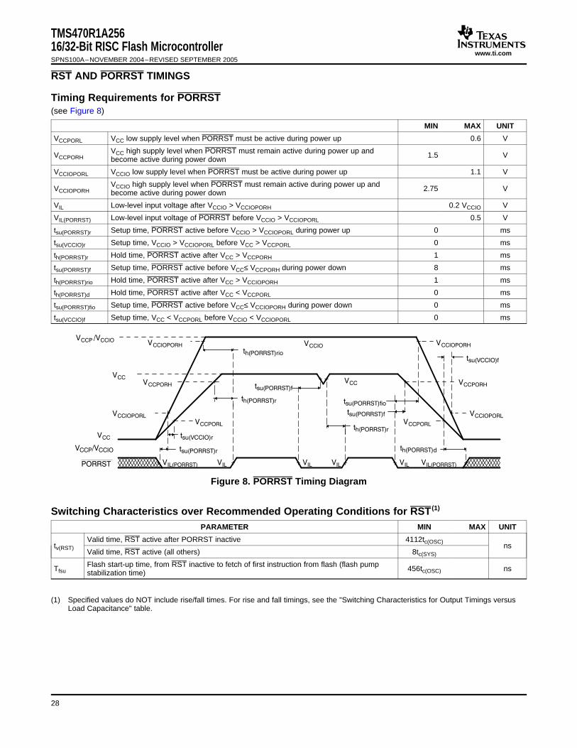
RST AND PORRST TIMINGS
Timing Requirements for PORRST
Switching Characteristics over Recommended Operating Conditions for RST (1)
TMS470R1A25616/32-Bit RISC Flash MicrocontrollerSPNS100A–NOVEMBER 2004–REVISED SEPTEMBER 2005
(see Figure 8)
MIN MAX UNIT
VCCPORL VCC low supply level when PORRST must be active during power up 0.6 V
VCC high supply level when PORRST must remain active during power up andVCCPORH 1.5 Vbecome active during power down
VCCIOPORL VCCIO low supply level when PORRST must be active during power up 1.1 V
VCCIO high supply level when PORRST must remain active during power up andVCCIOPORH 2.75 Vbecome active during power down
VIL Low-level input voltage after VCCIO > VCCIOPORH 0.2 VCCIO V
VIL(PORRST) Low-level input voltage of PORRST before VCCIO > VCCIOPORL 0.5 V
tsu(PORRST)r Setup time, PORRST active before VCCIO > VCCIOPORL during power up 0 ms
tsu(VCCIO)r Setup time, VCCIO > VCCIOPORL before VCC > VCCPORL 0 ms
th(PORRST)r Hold time, PORRST active after VCC > VCCPORH 1 ms
tsu(PORRST)f Setup time, PORRST active before VCC≤ VCCPORH during power down 8 ms
th(PORRST)rio Hold time, PORRST active after VCC > VCCIOPORH 1 ms
th(PORRST)d Hold time, PORRST active after VCC < VCCPORL 0 ms
tsu(PORRST)fio Setup time, PORRST active before VCC≤ VCCIOPORH during power down 0 ms
tsu(VCCIO)f Setup time, VCC < VCCPORL before VCCIO < VCCIOPORL 0 ms
Figure 8. PORRST Timing Diagram
PARAMETER MIN MAX UNIT
Valid time, RST active after PORRST inactive 4112tc(OSC)tv(RST) ns
Valid time, RST active (all others) 8tc(SYS)
Flash start-up time, from RST inactive to fetch of first instruction from flash (flash pumpTfsu 456tc(OSC) nsstabilization time)
(1) Specified values do NOT include rise/fall times. For rise and fall timings, see the "Switching Characteristics for Output Timings versusLoad Capacitance" table.
28
www.ti.com
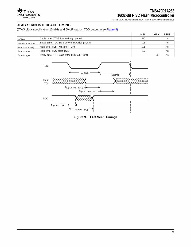
JTAG SCAN INTERFACE TIMING
TMS470R1A25616/32-Bit RISC Flash Microcontroller
SPNS100A–NOVEMBER 2004–REVISED SEPTEMBER 2005
(JTAG clock specification 10-MHz and 50-pF load on TDO output) (see Figure 9)
MIN MAX UNIT
tc(JTAG) Cycle time, JTAG low and high period 50 ns
tsu(TDI/TMS - TCKr) Setup time, TDI, TMS before TCK rise (TCKr) 15 ns
th(TCKr -TDI/TMS) Hold time, TDI, TMS after TCKr 15 ns
th(TCKf -TDO) Hold time, TDO after TCKf 10 ns
td(TCKf -TDO) Delay time, TDO valid after TCK fall (TCKf) 45 ns
Figure 9. JTAG Scan Timings
29
www.ti.com
OUTPUT TIMINGS
Switching Characteristics for Output Timings versus Load Capacitance (CL)
TMS470R1A25616/32-Bit RISC Flash MicrocontrollerSPNS100A–NOVEMBER 2004–REVISED SEPTEMBER 2005
(see Figure 10)
PARAMETER MIN MAX UNIT
CL = 15 pF 0.5 2.50
CL = 50 pF 1.5 5tr Rise time, CLKOUT, AWD, TDO ns
CL = 100 pF 3 9
CL = 150 pF 4.5 12.5
CL = 15 pF 0.5 2.5
CL = 50 pF 1.5 5tf Fall time, CLKOUT, AWD, TDO ns
CL = 100 pF 3 9
CL = 150 pF 4.5 12.5
CL = 15 pF 2.5 8
CL = 50 pF 5 14tr Rise time, SPInCLK, SPInSOMI, SPInSIMO (1) ns
CL = 100 pF 9 23
CL = 150 pF 13 32
CL = 15 pF 2.5 8
CL = 50 pF 5 14tf Fall time, RST, SPInCLK, SPInSOMI, SPInSIMO (1) ns
CL = 100 pF 9 23
CL = 150 pF 13 32
CL = 15 pF 2.5 10
CL = 50 pF 6.0 25tr Rise time, all other output pins ns
CL = 100 pF 12 45
CL = 150 pF 18 65
CL = 15 pF 3 10
CL = 50 pF 8.5 25tf Fall time, all other output pins ns
CL = 100 pF 16 45
CL = 150 pF 23 65
(1) Where n = 1 and 2
Figure 10. CMOS-Level Outputs
30
www.ti.com
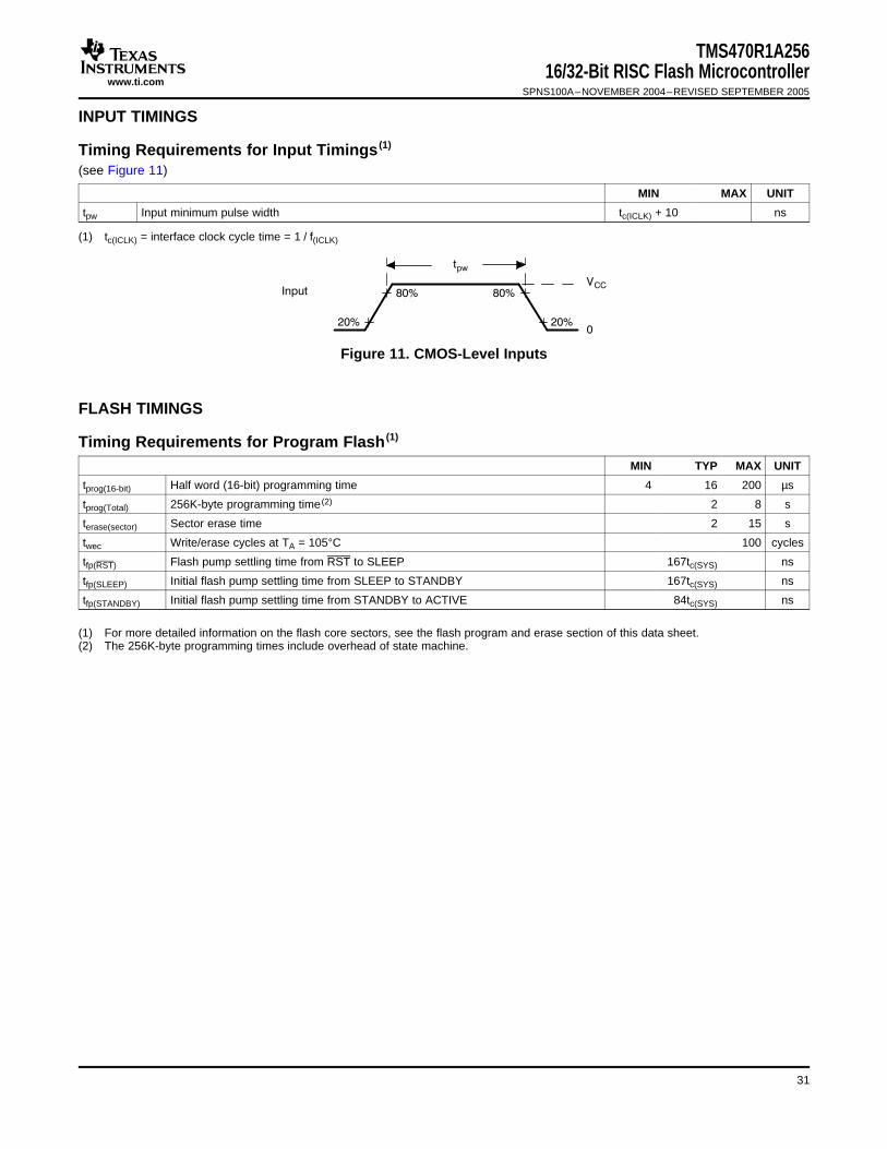
INPUT TIMINGS
Timing Requirements for Input Timings (1)
FLASH TIMINGS
Timing Requirements for Program Flash (1)
TMS470R1A25616/32-Bit RISC Flash Microcontroller
SPNS100A–NOVEMBER 2004–REVISED SEPTEMBER 2005
(see Figure 11)
MIN MAX UNIT
tpw Input minimum pulse width tc(ICLK) + 10 ns
(1) tc(ICLK) = interface clock cycle time = 1 / f(ICLK)
Figure 11. CMOS-Level Inputs
MIN TYP MAX UNIT
tprog(16-bit) Half word (16-bit) programming time 4 16 200 µs
tprog(Total) 256K-byte programming time (2) 2 8 s
terase(sector) Sector erase time 2 15 s
twec Write/erase cycles at TA = 105°C 100 cycles
tfp(RST) Flash pump settling time from RST to SLEEP 167tc(SYS) ns
tfp(SLEEP) Initial flash pump settling time from SLEEP to STANDBY 167tc(SYS) ns
tfp(STANDBY) Initial flash pump settling time from STANDBY to ACTIVE 84tc(SYS) ns
(1) For more detailed information on the flash core sectors, see the flash program and erase section of this data sheet.(2) The 256K-byte programming times include overhead of state machine.
31
www.ti.com
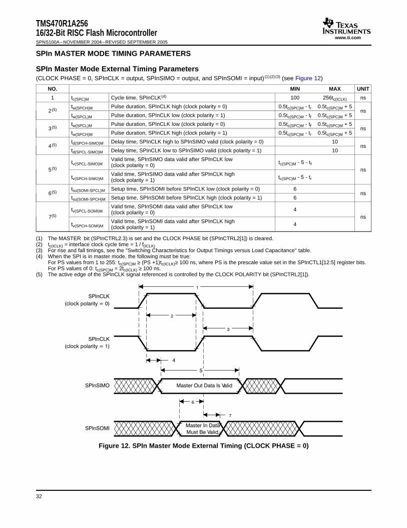
SPIn MASTER MODE TIMING PARAMETERS
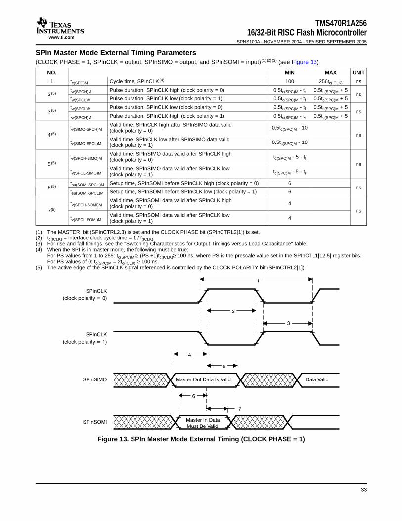
SPIn Master Mode External Timing Parameters
! "$&
! "$&
#$"$
%#$
#$"%$$#
TMS470R1A25616/32-Bit RISC Flash MicrocontrollerSPNS100A–NOVEMBER 2004–REVISED SEPTEMBER 2005
(CLOCK PHASE = 0, SPInCLK = output, SPInSIMO = output, and SPInSOMI = input) (1) (2) (3) (see Figure 12)
NO. MIN MAX UNIT
1 tc(SPC)M Cycle time, SPInCLK (4) 100 256tc(ICLK) ns
tw(SPCH)M Pulse duration, SPInCLK high (clock polarity = 0) 0.5tc(SPC)M - tr 0.5tc(SPC)M + 52 (5) ns
tw(SPCL)M Pulse duration, SPInCLK low (clock polarity = 1) 0.5tc(SPC)M - tf 0.5tc(SPC)M + 5
tw(SPCL)M Pulse duration, SPInCLK low (clock polarity = 0) 0.5tc(SPC)M - tf 0.5tc(SPC)M + 53 (5) ns
tw(SPCH)M Pulse duration, SPInCLK high (clock polarity = 1) 0.5tc(SPC)M - tr 0.5tc(SPC)M + 5
td(SPCH-SIMO)M Delay time, SPInCLK high to SPInSIMO valid (clock polarity = 0) 104 (5) ns
td(SPCL-SIMO)M Delay time, SPInCLK low to SPInSIMO valid (clock polarity = 1) 10
Valid time, SPInSIMO data valid after SPInCLK lowtv(SPCL-SIMO)M tc(SPC)M - 5 - tf(clock polarity = 0)5 (5) ns
Valid time, SPInSIMO data valid after SPInCLK hightv(SPCH-SIMO)M tc(SPC)M - 5 - tr(clock polarity = 1)
tsu(SOMI-SPCL)M Setup time, SPInSOMI before SPInCLK low (clock polarity = 0) 66 (5) ns
tsu(SOMI-SPCH)M Setup time, SPInSOMI before SPInCLK high (clock polarity = 1) 6
Valid time, SPInSOMI data valid after SPInCLK lowtv(SPCL-SOMI)M 4(clock polarity = 0)7(5) ns
Valid time, SPInSOMI data valid after SPInCLK hightv(SPCH-SOMI)M 4(clock polarity = 1)
(1) The MASTER bit (SPInCTRL2.3) is set and the CLOCK PHASE bit (SPInCTRL2[1]) is cleared.(2) tc(ICLK) = interface clock cycle time = 1 / f(ICLK)(3) For rise and fall timings, see the "Switching Characteristics for Output Timings versus Load Capacitance" table.(4) When the SPI is in master mode, the following must be true:
For PS values from 1 to 255: tc(SPC)M ≥ (PS +1)tc(ICLK)≥ 100 ns, where PS is the prescale value set in the SPInCTL1[12:5] register bits.For PS values of 0: tc(SPC)M = 2tc(ICLK) ≥ 100 ns.
(5) The active edge of the SPInCLK signal referenced is controlled by the CLOCK POLARITY bit (SPInCTRL2[1]).
Figure 12. SPIn Master Mode External Timing (CLOCK PHASE = 0)
32
www.ti.com
SPIn Master Mode External Timing Parameters
$
! "$&
! "$&
#$"$
%#$
#$"%$$#
TMS470R1A25616/32-Bit RISC Flash Microcontroller
SPNS100A–NOVEMBER 2004–REVISED SEPTEMBER 2005
(CLOCK PHASE = 1, SPInCLK = output, SPInSIMO = output, and SPInSOMI = input) (1) (2) (3) (see Figure 13)
NO. MIN MAX UNIT
1 tc(SPC)M Cycle time, SPInCLK (4) 100 256tc(ICLK) ns
tw(SPCH)M Pulse duration, SPInCLK high (clock polarity = 0) 0.5tc(SPC)M - tr 0.5tc(SPC)M + 52 (5) ns
tw(SPCL)M Pulse duration, SPInCLK low (clock polarity = 1) 0.5tc(SPC)M - tf 0.5tc(SPC)M + 5
tw(SPCL)M Pulse duration, SPInCLK low (clock polarity = 0) 0.5tc(SPC)M - tf 0.5tc(SPC)M + 53 (5) ns
tw(SPCH)M Pulse duration, SPInCLK high (clock polarity = 1) 0.5tc(SPC)M - tr 0.5tc(SPC)M + 5
Valid time, SPInCLK high after SPInSIMO data validtv(SIMO-SPCH)M 0.5tc(SPC)M - 10(clock polarity = 0)4 (5) ns
Valid time, SPInCLK low after SPInSIMO data validtv(SIMO-SPCL)M 0.5tc(SPC)M - 10(clock polarity = 1)
Valid time, SPInSIMO data valid after SPInCLK hightv(SPCH-SIMO)M tc(SPC)M - 5 - tf(clock polarity = 0)5 (5) ns
Valid time, SPInSIMO data valid after SPInCLK lowtv(SPCL-SIMO)M tc(SPC)M - 5 - tr(clock polarity = 1)
tsu(SOMI-SPCH)M Setup time, SPInSOMI before SPInCLK high (clock polarity = 0) 66 (5) ns
tsu(SOMI-SPCL)M Setup time, SPInSOMI before SPInCLK low (clock polarity = 1) 6
Valid time, SPInSOMI data valid after SPInCLK hightv(SPCH-SOMI)M 4(clock polarity = 0)7(5) ns
Valid time, SPInSOMI data valid after SPInCLK lowtv(SPCL-SOMI)M 4(clock polarity = 1)
(1) The MASTER bit (SPInCTRL2.3) is set and the CLOCK PHASE bit (SPInCTRL2[1]) is set.(2) tc(ICLK) = interface clock cycle time = 1 / f(ICLK)(3) For rise and fall timings, see the "Switching Characteristics for Output Timings versus Load Capacitance" table.(4) When the SPI is in master mode, the following must be true:
For PS values from 1 to 255: tc(SPC)M ≥ (PS +1)tc(ICLK)≥ 100 ns, where PS is the prescale value set in the SPInCTL1[12:5] register bits.For PS values of 0: tc(SPC)M = 2tc(ICLK) ≥ 100 ns.
(5) The active edge of the SPInCLK signal referenced is controlled by the CLOCK POLARITY bit (SPInCTRL2[1]).
Figure 13. SPIn Master Mode External Timing (CLOCK PHASE = 1)
33
www.ti.com
SPIn SLAVE MODE TIMING PARAMETERS
SPIn Slave Mode External Timing Parameters
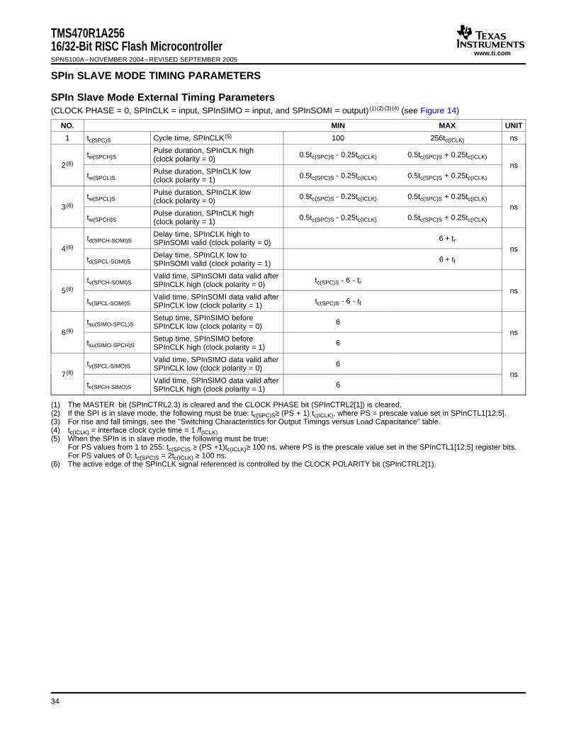
TMS470R1A25616/32-Bit RISC Flash MicrocontrollerSPNS100A–NOVEMBER 2004–REVISED SEPTEMBER 2005
(CLOCK PHASE = 0, SPInCLK = input, SPInSIMO = input, and SPInSOMI = output) (1) (2) (3) (4) (see Figure 14)
NO. MIN MAX UNIT
1 tc(SPC)S Cycle time, SPInCLK (5) 100 256tc(ICLK) ns
Pulse duration, SPInCLK hightw(SPCH)S 0.5tc(SPC)S - 0.25tc(ICLK) 0.5tc(SPC)S + 0.25tc(ICLK)(clock polarity = 0)2 (6) ns
Pulse duration, SPInCLK lowtw(SPCL)S 0.5tc(SPC)S - 0.25tc(ICLK) 0.5tc(SPC)S + 0.25tc(ICLK)(clock polarity = 1)
Pulse duration, SPInCLK lowtw(SPCL)S 0.5tc(SPC)S - 0.25tc(ICLK) 0.5tc(SPC)S + 0.25tc(ICLK)(clock polarity = 0)3 (6) ns
Pulse duration, SPInCLK hightw(SPCH)S 0.5tc(SPC)S - 0.25tc(ICLK) 0.5tc(SPC)S + 0.25tc(ICLK)(clock polarity = 1)
Delay time, SPInCLK high totd(SPCH-SOMI)S 6 + trSPInSOMI valid (clock polarity = 0)4 (6) ns
Delay time, SPInCLK low totd(SPCL-SOMI)S 6 + tfSPInSOMI valid (clock polarity = 1)
Valid time, SPInSOMI data valid aftertv(SPCH-SOMI)S tc(SPC)S - 6 - trSPInCLK high (clock polarity = 0)5 (6) ns
Valid time, SPInSOMI data valid aftertv(SPCL-SOMI)S tc(SPC)S - 6 - tfSPInCLK low (clock polarity = 1)
Setup time, SPInSIMO beforetsu(SIMO-SPCL)S 6SPInCLK low (clock polarity = 0)6 (6) ns
Setup time, SPInSIMO beforetsu(SIMO-SPCH)S 6SPInCLK high (clock polarity = 1)
Valid time, SPInSIMO data valid aftertv(SPCL-SIMO)S 6SPInCLK low (clock polarity = 0)7 (6) ns
Valid time, SPInSIMO data valid aftertv(SPCH-SIMO)S 6SPInCLK high (clock polarity = 1)
(1) The MASTER bit (SPInCTRL2.3) is cleared and the CLOCK PHASE bit (SPInCTRL2[1]) is cleared.(2) If the SPI is in slave mode, the following must be true: tc(SPC)S≥ (PS + 1) tc(ICLK), where PS = prescale value set in SPInCTL1[12:5].(3) For rise and fall timings, see the "Switching Characteristics for Output Timings versus Load Capacitance" table.(4) tc(ICLK) = interface clock cycle time = 1 /f(ICLK)(5) When the SPIn is in slave mode, the following must be true:
For PS values from 1 to 255: tc(SPC)S ≥ (PS +1)tc(ICLK)≥ 100 ns, where PS is the prescale value set in the SPInCTL1[12:5] register bits.For PS values of 0: tc(SPC)S = 2tc(ICLK) ≥ 100 ns.
(6) The active edge of the SPInCLK signal referenced is controlled by the CLOCK POLARITY bit (SPInCTRL2[1).
34
www.ti.com
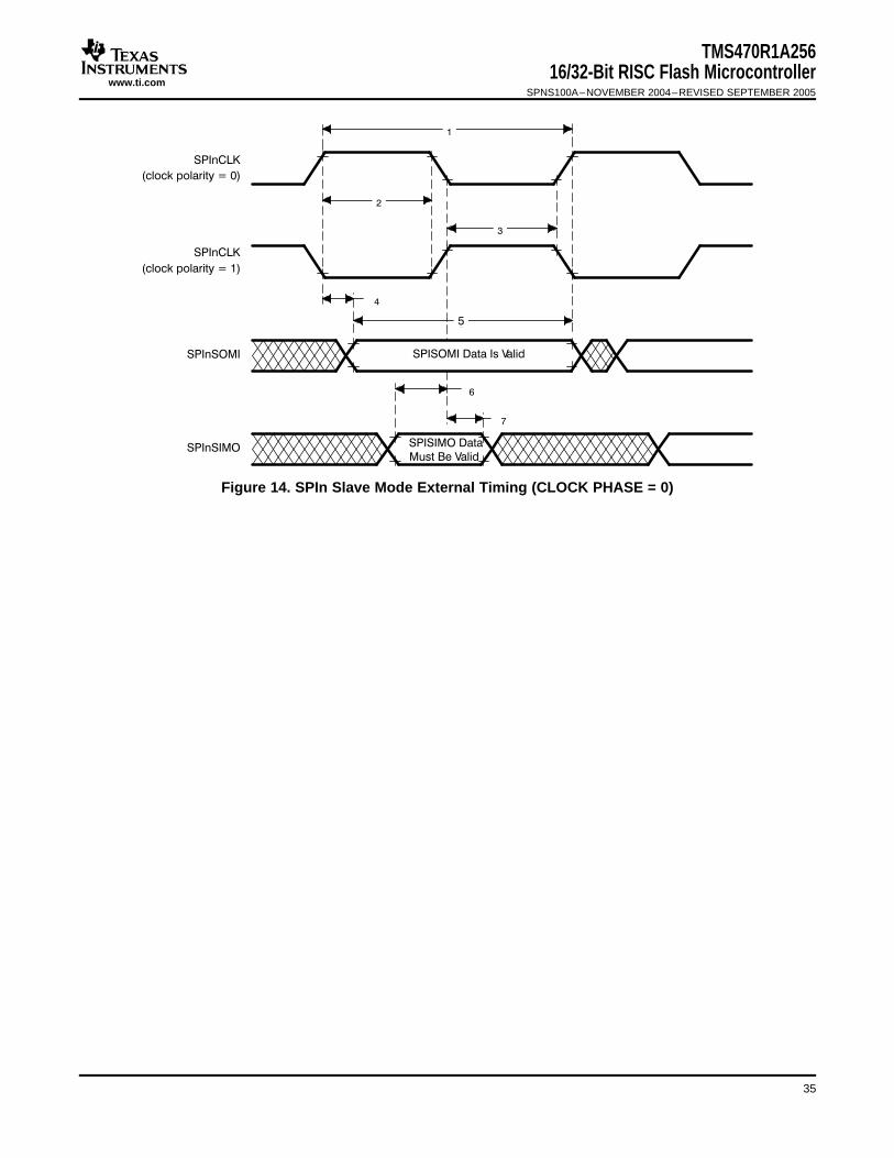
! "$&
! "$&
$
%#$
$#
TMS470R1A25616/32-Bit RISC Flash Microcontroller
SPNS100A–NOVEMBER 2004–REVISED SEPTEMBER 2005
Figure 14. SPIn Slave Mode External Timing (CLOCK PHASE = 0)
35
www.ti.com
SPIn Slave Mode External Timing Parameters
TMS470R1A25616/32-Bit RISC Flash MicrocontrollerSPNS100A–NOVEMBER 2004–REVISED SEPTEMBER 2005
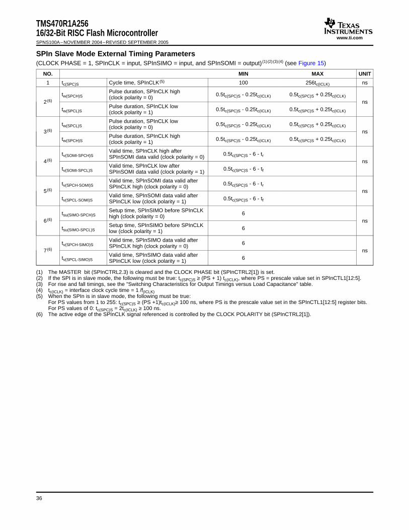
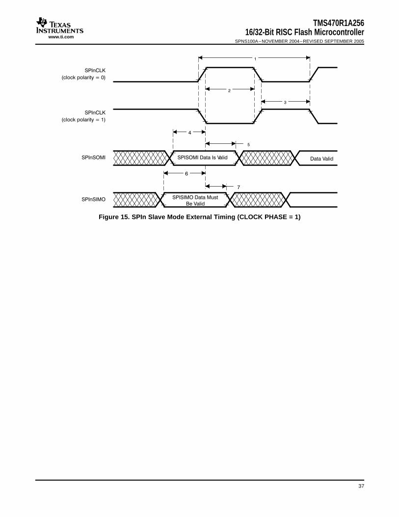
(CLOCK PHASE = 1, SPInCLK = input, SPInSIMO = input, and SPInSOMI = output) (1) (2) (3) (4) (see Figure 15)
NO. MIN MAX UNIT
1 tc(SPC)S Cycle time, SPInCLK (5) 100 256tc(ICLK) ns
Pulse duration, SPInCLK hightw(SPCH)S 0.5tc(SPC)S - 0.25tc(ICLK) 0.5tc(SPC)S + 0.25tc(ICLK)(clock polarity = 0)2 (6) ns
Pulse duration, SPInCLK lowtw(SPCL)S 0.5tc(SPC)S - 0.25tc(ICLK) 0.5tc(SPC)S + 0.25tc(ICLK)(clock polarity = 1)
Pulse duration, SPInCLK lowtw(SPCL)S 0.5tc(SPC)S - 0.25tc(ICLK) 0.5tc(SPC)S + 0.25tc(ICLK)(clock polarity = 0)3 (6) ns
Pulse duration, SPInCLK hightw(SPCH)S 0.5tc(SPC)S - 0.25tc(ICLK) 0.5tc(SPC)S + 0.25tc(ICLK)(clock polarity = 1)
Valid time, SPInCLK high aftertv(SOMI-SPCH)S 0.5tc(SPC)S - 6 - trSPInSOMI data valid (clock polarity = 0)4 (6) ns
Valid time, SPInCLK low aftertv(SOMI-SPCL)S 0.5tc(SPC)S - 6 - tfSPInSOMI data valid (clock polarity = 1)
Valid time, SPInSOMI data valid aftertv(SPCH-SOMI)S 0.5tc(SPC)S - 6 - trSPInCLK high (clock polarity = 0)5 (6) ns
Valid time, SPInSOMI data valid aftertv(SPCL-SOMI)S 0.5tc(SPC)S - 6 - tfSPInCLK low (clock polarity = 1)
Setup time, SPInSIMO before SPInCLKtsu(SIMO-SPCH)S 6high (clock polarity = 0)6 (6) ns
Setup time, SPInSIMO before SPInCLKtsu(SIMO-SPCL)S 6low (clock polarity = 1)
Valid time, SPInSIMO data valid aftertv(SPCH-SIMO)S 6SPInCLK high (clock polarity = 0)7 (6) ns
Valid time, SPInSIMO data valid aftertv(SPCL-SIMO)S 6SPInCLK low (clock polarity = 1)
(1) The MASTER bit (SPInCTRL2.3) is cleared and the CLOCK PHASE bit (SPInCTRL2[1]) is set.(2) If the SPI is in slave mode, the following must be true: tc(SPC)S ≥ (PS + 1) tc(ICLK), where PS = prescale value set in SPInCTL1[12:5].(3) For rise and fall timings, see the "Switching Characteristics for Output Timings versus Load Capacitance" table.(4) tc(ICLK) = interface clock cycle time = 1 /f(ICLK)(5) When the SPIn is in slave mode, the following must be true:
For PS values from 1 to 255: tc(SPC)S ≥ (PS +1)tc(ICLK)≥ 100 ns, where PS is the prescale value set in the SPInCTL1[12:5] register bits.For PS values of 0: tc(SPC)S = 2tc(ICLK) ≥ 100 ns.
(6) The active edge of the SPInCLK signal referenced is controlled by the CLOCK POLARITY bit (SPInCTRL2[1]).
36
www.ti.com
$
! "$&
! "$&
$%#$
$#
TMS470R1A25616/32-Bit RISC Flash Microcontroller
SPNS100A–NOVEMBER 2004–REVISED SEPTEMBER 2005
Figure 15. SPIn Slave Mode External Timing (CLOCK PHASE = 1)
37
www.ti.com
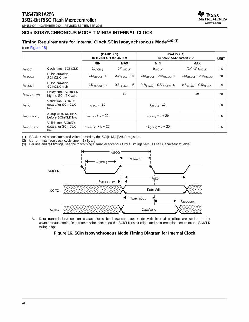
SCIn ISOSYNCHRONOUS MODE TIMINGS INTERNAL CLOCK
Timing Requirements for Internal Clock SCIn Isosynchronous Mode (1) (2) (3)
TMS470R1A25616/32-Bit RISC Flash MicrocontrollerSPNS100A–NOVEMBER 2004–REVISED SEPTEMBER 2005
(see Figure 16)
(BAUD + 1) (BAUD + 1)IS EVEN OR BAUD = 0 IS ODD AND BAUD ≠ 0 UNIT
MIN MAX MIN MAX
tc(SCC) Cycle time, SCInCLK 2tc(ICLK) 224tc(ICLK) 3tc(ICLK) (224 -1) tc(ICLK) ns
Pulse duration,tw(SCCL) 0.5tc(SCC) - tf 0.5tc(SCC) + 5 0.5tc(SCC) + 0.5tc(ICLK)- tf 0.5tc(SCC) + 0.5tc(ICLK) nsSCInCLK low
Pulse duration,tw(SCCH) 0.5tc(SCC) - tr 0.5tc(SCC) + 5 0.5tc(SCC) - 0.5tc(ICLK)- tr 0.5tc(SCC) - 0.5tc(ICLK) nsSCInCLK high
Delay time, SCInCLKtd(SCCH-TXV) 10 10 nshigh to SCInTX valid
Valid time, SCInTXtv(TX) data after SCInCLK tc(SCC) - 10 tc(SCC) - 10 ns
low
Setup time, SCInRXtsu(RX-SCCL) tc(ICLK) + tf + 20 tc(ICLK) + tf + 20 nsbefore SCInCLK low
Valid time, SCInRXtv(SCCL-RX) data after SCInCLK - tc(ICLK) + tf + 20 - tc(ICLK) + tf + 20 ns
low
(1) BAUD = 24-bit concatenated value formed by the SCI[H,M,L]BAUD registers.(2) tc(ICLK) = interface clock cycle time = 1 / f(ICLK)(3) For rise and fall timings, see the "Switching Characteristics for Output Timings versus Load Capacitance" table.
A. Data transmission/reception characteristics for isosynchronous mode with internal clocking are similar to theasynchronous mode. Data transmission occurs on the SCICLK rising edge, and data reception occurs on the SCICLKfalling edge.
Figure 16. SCIn Isosynchronous Mode Timing Diagram for Internal Clock
38
www.ti.com
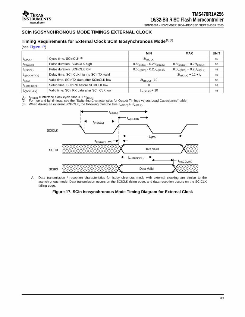
SCIn ISOSYNCHRONOUS MODE TIMINGS EXTERNAL CLOCK
Timing Requirements for External Clock SCIn Isosynchronous Mode (1) (2)
TMS470R1A25616/32-Bit RISC Flash Microcontroller
SPNS100A–NOVEMBER 2004–REVISED SEPTEMBER 2005
(see Figure 17)
MIN MAX UNIT
tc(SCC) Cycle time, SCInCLK (3) 8tc(ICLK) ns
tw(SCCH) Pulse duration, SCInCLK high 0.5tc(SCC) - 0.25tc(ICLK) 0.5tc(SCC) + 0.25tc(ICLK) ns
tw(SCCL) Pulse duration, SCInCLK low 0.5tc(SCC) - 0.25tc(ICLK) 0.5tc(SCC) + 0.25tc(ICLK) ns
td(SCCH-TXV) Delay time, SCInCLK high to SCInTX valid 2tc(ICLK) + 12 + tr ns
tv(TX) Valid time, SCInTX data after SCInCLK low 2tc(SCC) - 10 ns
tsu(RX-SCCL) Setup time, SCInRX before SCInCLK low 0 ns
tv(SCCL-RX) Valid time, SCInRX data after SCInCLK low 2tc(ICLK) + 10 ns
(1) tc(ICLK) = interface clock cycle time = 1 / f(ICLK)(2) For rise and fall timings, see the "Switching Characteristics for Output Timings versus Load Capacitance" table.(3) When driving an external SCInCLK, the following must be true: tc(SCC) ≥ 8tc(ICLK)
A. Data transmission / reception characteristics for isosynchronous mode with external clocking are similar to theasynchronous mode. Data transmission occurs on the SCICLK rising edge, and data reception occurs on the SCICLKfalling edge.
Figure 17. SCIn Isosynchronous Mode Timing Diagram for External Clock
39
www.ti.com
HIGH-END TIMER (HET) TIMINGS
Minimum PWM Output Pulse Width:
Minimum Input Pulses that Can Be Captured:
STANDARD CAN CONTROLLER (SCC) MODE TIMINGS
Dynamic Characteristics for the CANSTX and CANSRX Pins
TMS470R1A25616/32-Bit RISC Flash MicrocontrollerSPNS100A–NOVEMBER 2004–REVISED SEPTEMBER 2005
This is equal to one high resolution clock period (HRP). The HRP is defined by the 6-bit high resolution prescalefactor (hr), which is user defined, giving prescale factors of 1 to 64, with a linear increment of codes.
Therefore, the minimum PWM output pulse width = HRP(min) = hr(min)/SYSCLK = 1/SYSCLK
For example, for a SYSCLK of 30 MHz, the minimum PWM output pulse width = 1/30 = 33.33ns
The input pulse width must be greater or equal to the low resolution clock period (LRP), i.e., the HET loop (theHET program must fit within the LRP). The LRP is defined by the 3-bit loop-resolution prescale factor (lr), whichis user defined, with a power of 2 increment of codes. That is, the value of lr can be 1, 2, 4, 8, 16, or 32.
Therefore, the minimum input pulse width = LRP(min) = hr(min) * lr(min)/SYSCLK = 1 * 1/SYSCLK
For example, with a SYSCLK of 30 MHz, the minimum input pulse width = 1 * 1/30 = 33.33 ns
NOTE:
Once the input pulse width is greater than LRP, the resolution of the measurement isstill HRP. (That is, the captured value gives the number of HRP clocks inside thepulse.)
Abbreviations:
hr = HET high resolution divide rate = 1, 2, 3,...63, 64
lr = HET low resolution divide rate = 1, 2, 4, 8, 16, 32
High resolution clock period = HRP = hr/SYSCLK
Loop resolution clock period = LRP = hr*lr/SYSCLK
PARAMETER MIN MAX UNIT
td(CANSTX) Delay time, transmit shift register to CANSTX pin (1) 15 ns
td(CANSRX) Delay time, CANSRX pin to receive shift register 5 ns
(1) These values do not include the rise/fall times of the output buffer.
40
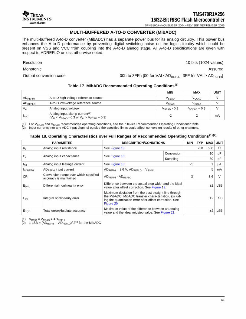
www.ti.com
MULTI-BUFFERED A-TO-D CONVERTER (MibADC)
TMS470R1A25616/32-Bit RISC Flash Microcontroller
SPNS100A–NOVEMBER 2004–REVISED SEPTEMBER 2005
The multi-buffered A-to-D converter (MibADC) has a separate power bus for its analog circuitry. This power busenhances the A-to-D performance by preventing digital switching noise on the logic circuitry which could bepresent on VSS and VCC from coupling into the A-to-D analog stage. All A-to-D specifications are given withrespect to ADREFLO unless otherwise noted.
Resolution 10 bits (1024 values)
Monotonic Assured
Output conversion code 00h to 3FFh [00 for VAI ≤ADREFLO; 3FF for VAI ≥ ADREFHI]
Table 17. MibADC Recommended Operating Conditions (1)
MIN MAX UNIT
ADREFHI A-to-D high-voltage reference source VSSAD VCCAD V
ADREFLO A-to-D low-voltage reference source VSSAD VCCAD V
VAI Analog input voltage VSSAD - 0.3 VCCAD + 0.3 V
Analog input clamp current (2)IAIC -2 2 mA(VAI < VSSAD - 0.3 or VAI > VCCAD + 0.3)
(1) For VCCAD and VSSAD recommended operating conditions, see the "Device Recommended Operating Conditions" table.(2) Input currents into any ADC input channel outside the specified limits could affect conversion results of other channels.
Table 18. Operating Characteristics over Full Ranges of Recommended Operating Conditions (1) (2)
PARAMETER DESCRIPTION/CONDITIONS MIN TYP MAX UNIT
Ri Analog input resistance See Figure 18. 250 500 Ω
Conversion 10 pFCi Analog input capacitance See Figure 18.
Sampling 30 pF
IAIL Analog input leakage current See Figure 18. -1 1 µA
IADREFHI ADREFHI input current ADREFHI = 3.6 V, ADREFLO = VSSAD 5 mA
Conversion range over which specifiedCR ADREFHI - ADREFLO 3 3.6 Vaccuracy is maintained
Difference between the actual step width and the idealEDNL Differential nonlinearity error ±2 LSBvalue after offset correction. See Figure 19.
Maximum deviation from the best straight line throughthe MibADC. MibADC transfer characteristics, exclud-EINL Integral nonlinearity error ±2 LSBing the quantization error after offset correction. SeeFigure 20.
Maximum value of the difference between an analogETOT Total error/Absolute accuracy ±2 LSBvalue and the ideal midstep value. See Figure 21.
(1) VCCIO = VCCAD = ADREFHI(2) 1 LSB = (ADREFHI - ADREFLO)/ 210 for the MibADC
41
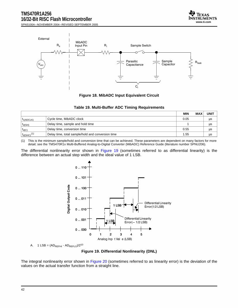
www.ti.com
!
!
TMS470R1A25616/32-Bit RISC Flash MicrocontrollerSPNS100A–NOVEMBER 2004–REVISED SEPTEMBER 2005
Figure 18. MibADC Input Equivalent Circuit
Table 19. Multi-Buffer ADC Timing Requirements
MIN MAX UNIT
tc(ADCLK) Cycle time, MibADC clock 0.05 µs
td(SH) Delay time, sample and hold time 1 µs
td(C) Delay time, conversion time 0.55 µs
td(SHC)(1) Delay time, total sample/hold and conversion time 1.55 µs
(1) This is the minimum sample/hold and conversion time that can be achieved. These parameters are dependent on many factors for moredetail; see the TMS470R1x Multi-Buffered Analog-to-Digital Converter (MibADC) Reference Guide (literature number SPNU206).
The differential nonlinearity error shown in Figure 19 (sometimes referred to as differential linearity) is thedifference between an actual step width and the ideal value of 1 LSB.
A. 1 LSB = (ADREFHI - ADREFLO)/210
Figure 19. Differential Nonlinearity (DNL)
The integral nonlinearity error shown in Figure 20 (sometimes referred to as linearity error) is the deviation of thevalues on the actual transfer function from a straight line.
42
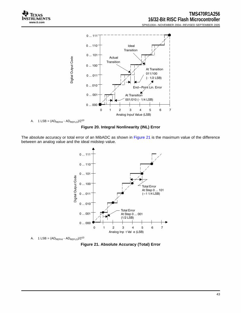
www.ti.com
!%$%
$"#$
&
$"" "
$"#$
&
"#$
$%
"#$
TMS470R1A25616/32-Bit RISC Flash Microcontroller
SPNS100A–NOVEMBER 2004–REVISED SEPTEMBER 2005
A. 1 LSB = (ADREFHI - ADREFLO)/210
Figure 20. Integral Nonlinearity (INL) Error
The absolute accuracy or total error of an MibADC as shown in Figure 21 is the maximum value of the differencebetween an analog value and the ideal midstep value.
A. 1 LSB = (ADREFHI - ADREFLO)/210
Figure 21. Absolute Accuracy (Total) Error
43

www.ti.com
THERMAL CHARACTERISTICS
TMS470R1A25616/32-Bit RISC Flash MicrocontrollerSPNS100A–NOVEMBER 2004–REVISED SEPTEMBER 2005
PARAMETER °C/W
RΘJA 51
RΘJC 5
44
www.ti.com
TMS470R1A25616/32-Bit RISC Flash Microcontroller
SPNS100A–NOVEMBER 2004–REVISED SEPTEMBER 2005
REVISION HISTORY
This revision history highlights the changes made to the device-specific datasheet SPNS100 to create theSPNS100A version.
Table 7. Revision History
Changed Figure 2, the Family Nomenclature drawing, to reflect T version of the temperature range.
Revised "Absolute Maximum Ratings over Operating Free-Air Temperature Range" table to show T version of the temperature range.
Revised "Device Recommended Operating Conditions" table to show T version of the temperature range.
Added "Device and Development-Support Tool Nomenclature" information.
Changed VCC to 2.06 V in the ICC in the "Electrical Characteristics over Recommended Operating Free-Air Temperature Range" table.
Changed the max for the ICC Digital supply current (operating mode) at SYSCLK = 48 MHz from 75 to 70 mA.
Corrected VCCPORE to VCCPORL in "Timing Requirements for PORRST" table.
Moved 2.75 from Max to Min column for VCCIOPORH in "Timing Requirements for PORRST" table.
Added row for Tfsu to "Switching Characteristics over Recommended Operating Conditions for RST" table.
Added rows for Tfp(RST), Tfp(SLEEP), and Tfp(STANDBY) to "Flash Timings" table.
45
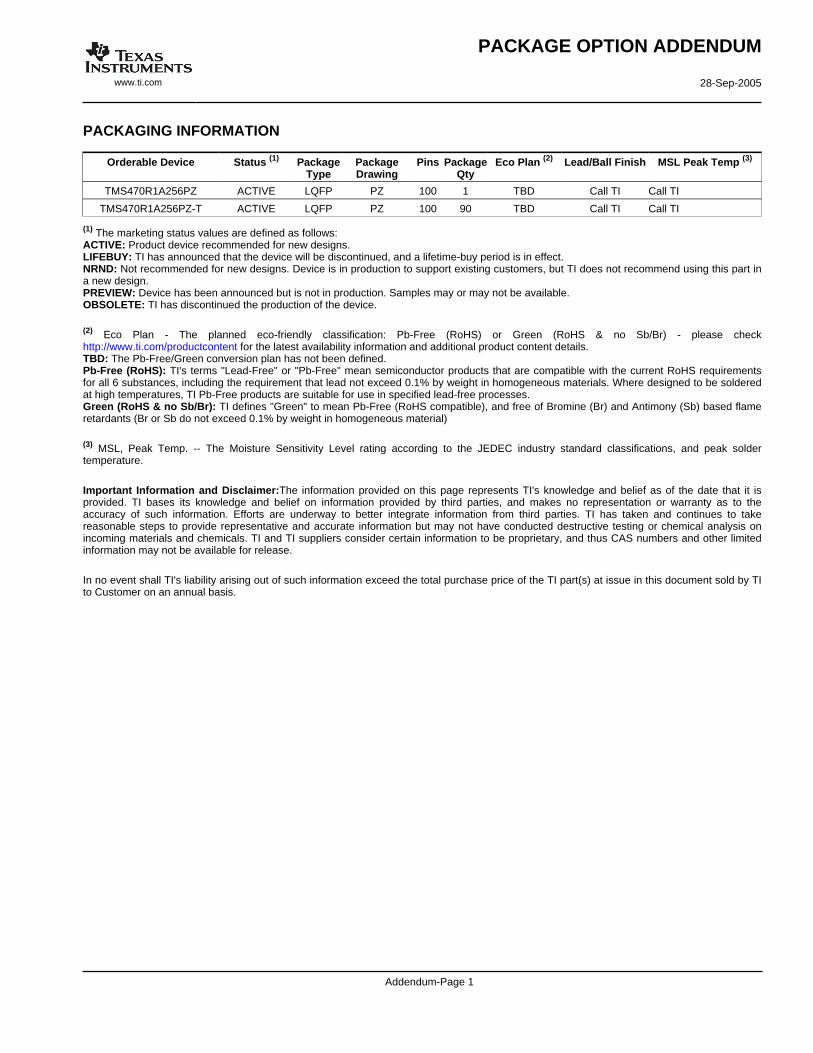
PACKAGING INFORMATION
Orderable Device Status (1) PackageType
PackageDrawing
Pins PackageQty
Eco Plan (2) Lead/Ball Finish MSL Peak Temp (3)
TMS470R1A256PZ ACTIVE LQFP PZ 100 1 TBD Call TI Call TI
TMS470R1A256PZ-T ACTIVE LQFP PZ 100 90 TBD Call TI Call TI
(1) The marketing status values are defined as follows:ACTIVE: Product device recommended for new designs.LIFEBUY: TI has announced that the device will be discontinued, and a lifetime-buy period is in effect.NRND: Not recommended for new designs. Device is in production to support existing customers, but TI does not recommend using this part ina new design.PREVIEW: Device has been announced but is not in production. Samples may or may not be available.OBSOLETE: TI has discontinued the production of the device.
(2) Eco Plan - The planned eco-friendly classification: Pb-Free (RoHS) or Green (RoHS & no Sb/Br) - please checkhttp://www.ti.com/productcontent for the latest availability information and additional product content details.TBD: The Pb-Free/Green conversion plan has not been defined.Pb-Free (RoHS): TI's terms "Lead-Free" or "Pb-Free" mean semiconductor products that are compatible with the current RoHS requirementsfor all 6 substances, including the requirement that lead not exceed 0.1% by weight in homogeneous materials. Where designed to be solderedat high temperatures, TI Pb-Free products are suitable for use in specified lead-free processes.Green (RoHS & no Sb/Br): TI defines "Green" to mean Pb-Free (RoHS compatible), and free of Bromine (Br) and Antimony (Sb) based flameretardants (Br or Sb do not exceed 0.1% by weight in homogeneous material)
(3) MSL, Peak Temp. -- The Moisture Sensitivity Level rating according to the JEDEC industry standard classifications, and peak soldertemperature.
Important Information and Disclaimer:The information provided on this page represents TI's knowledge and belief as of the date that it isprovided. TI bases its knowledge and belief on information provided by third parties, and makes no representation or warranty as to theaccuracy of such information. Efforts are underway to better integrate information from third parties. TI has taken and continues to takereasonable steps to provide representative and accurate information but may not have conducted destructive testing or chemical analysis onincoming materials and chemicals. TI and TI suppliers consider certain information to be proprietary, and thus CAS numbers and other limitedinformation may not be available for release.
In no event shall TI's liability arising out of such information exceed the total purchase price of the TI part(s) at issue in this document sold by TIto Customer on an annual basis.
PACKAGE OPTION ADDENDUM
www.ti.com 28-Sep-2005
Addendum-Page 1
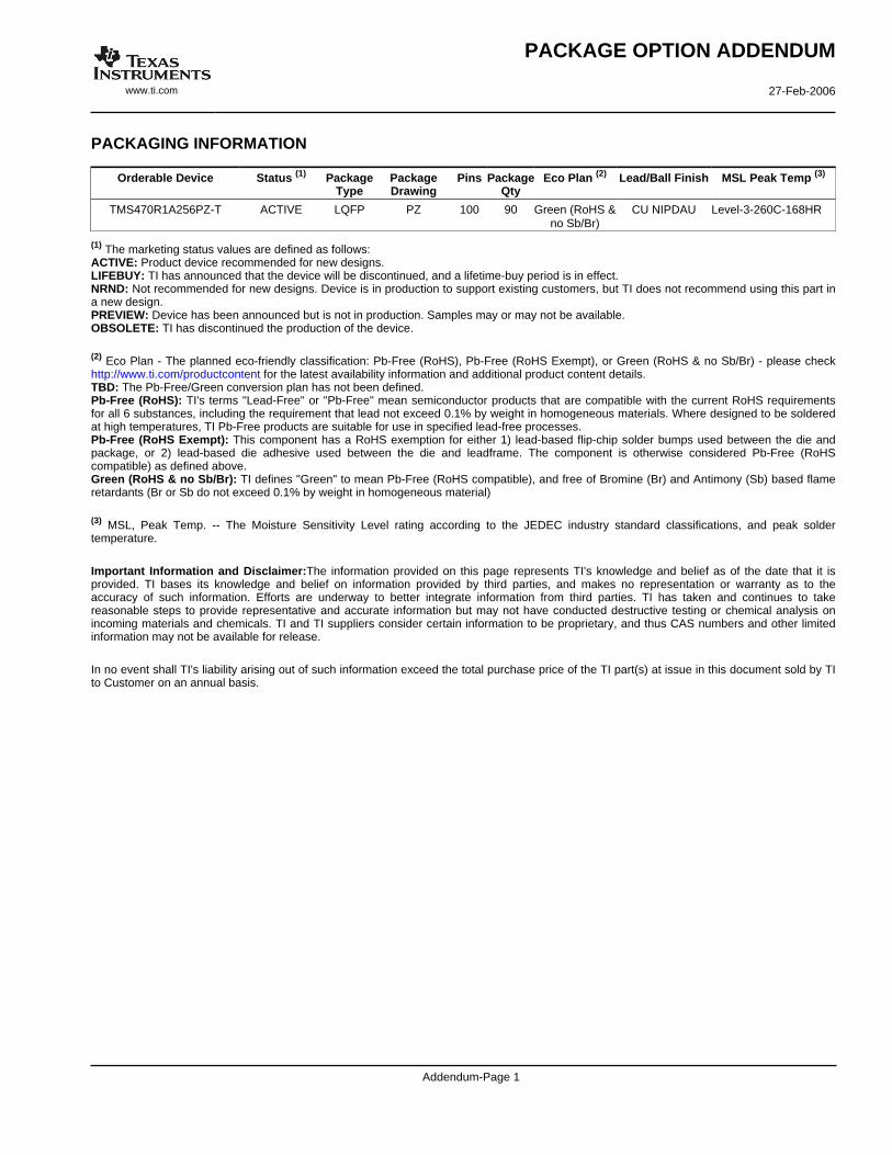
PACKAGING INFORMATION
Orderable Device Status (1) PackageType
PackageDrawing
Pins PackageQty
Eco Plan (2) Lead/Ball Finish MSL Peak Temp (3)
TMS470R1A256PZ-T ACTIVE LQFP PZ 100 90 Green (RoHS &no Sb/Br)
CU NIPDAU Level-3-260C-168HR
(1) The marketing status values are defined as follows:ACTIVE: Product device recommended for new designs.LIFEBUY: TI has announced that the device will be discontinued, and a lifetime-buy period is in effect.NRND: Not recommended for new designs. Device is in production to support existing customers, but TI does not recommend using this part ina new design.PREVIEW: Device has been announced but is not in production. Samples may or may not be available.OBSOLETE: TI has discontinued the production of the device.
(2) Eco Plan - The planned eco-friendly classification: Pb-Free (RoHS), Pb-Free (RoHS Exempt), or Green (RoHS & no Sb/Br) - please checkhttp://www.ti.com/productcontent for the latest availability information and additional product content details.TBD: The Pb-Free/Green conversion plan has not been defined.Pb-Free (RoHS): TI's terms "Lead-Free" or "Pb-Free" mean semiconductor products that are compatible with the current RoHS requirementsfor all 6 substances, including the requirement that lead not exceed 0.1% by weight in homogeneous materials. Where designed to be solderedat high temperatures, TI Pb-Free products are suitable for use in specified lead-free processes.Pb-Free (RoHS Exempt): This component has a RoHS exemption for either 1) lead-based flip-chip solder bumps used between the die andpackage, or 2) lead-based die adhesive used between the die and leadframe. The component is otherwise considered Pb-Free (RoHScompatible) as defined above.Green (RoHS & no Sb/Br): TI defines "Green" to mean Pb-Free (RoHS compatible), and free of Bromine (Br) and Antimony (Sb) based flameretardants (Br or Sb do not exceed 0.1% by weight in homogeneous material)
(3) MSL, Peak Temp. -- The Moisture Sensitivity Level rating according to the JEDEC industry standard classifications, and peak soldertemperature.
Important Information and Disclaimer:The information provided on this page represents TI's knowledge and belief as of the date that it isprovided. TI bases its knowledge and belief on information provided by third parties, and makes no representation or warranty as to theaccuracy of such information. Efforts are underway to better integrate information from third parties. TI has taken and continues to takereasonable steps to provide representative and accurate information but may not have conducted destructive testing or chemical analysis onincoming materials and chemicals. TI and TI suppliers consider certain information to be proprietary, and thus CAS numbers and other limitedinformation may not be available for release.
In no event shall TI's liability arising out of such information exceed the total purchase price of the TI part(s) at issue in this document sold by TIto Customer on an annual basis.
PACKAGE OPTION ADDENDUM
www.ti.com 27-Feb-2006
Addendum-Page 1
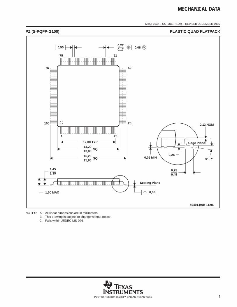
MECHANICAL DATA
MTQF013A – OCTOBER 1994 – REVISED DECEMBER 1996
1POST OFFICE BOX 655303 • DALLAS, TEXAS 75265
PZ (S-PQFP-G100) PLASTIC QUAD FLATPACK
4040149/B 11/96
50
26 0,13 NOM
Gage Plane
0,25
0,450,75
0,05 MIN
0,27
51
25
75
1
12,00 TYP
0,17
76
100
SQ
SQ15,8016,20
13,80
1,351,45
1,60 MAX
14,20
0°–7°
Seating Plane
0,08
0,50 M0,08
NOTES: A. All linear dimensions are in millimeters.B. This drawing is subject to change without notice.C. Falls within JEDEC MS-026
IMPORTANT NOTICE
Texas Instruments Incorporated and its subsidiaries (TI) reserve the right to make corrections, modifications,enhancements, improvements, and other changes to its products and services at any time and to discontinueany product or service without notice. Customers should obtain the latest relevant information before placingorders and should verify that such information is current and complete. All products are sold subject to TI’s termsand conditions of sale supplied at the time of order acknowledgment.
TI warrants performance of its hardware products to the specifications applicable at the time of sale inaccordance with TI’s standard warranty. Testing and other quality control techniques are used to the extent TIdeems necessary to support this warranty. Except where mandated by government requirements, testing of allparameters of each product is not necessarily performed.
TI assumes no liability for applications assistance or customer product design. Customers are responsible fortheir products and applications using TI components. To minimize the risks associated with customer productsand applications, customers should provide adequate design and operating safeguards.
TI does not warrant or represent that any license, either express or implied, is granted under any TI patent right,copyright, mask work right, or other TI intellectual property right relating to any combination, machine, or processin which TI products or services are used. Information published by TI regarding third-party products or servicesdoes not constitute a license from TI to use such products or services or a warranty or endorsement thereof.Use of such information may require a license from a third party under the patents or other intellectual propertyof the third party, or a license from TI under the patents or other intellectual property of TI.
Reproduction of information in TI data books or data sheets is permissible only if reproduction is withoutalteration and is accompanied by all associated warranties, conditions, limitations, and notices. Reproductionof this information with alteration is an unfair and deceptive business practice. TI is not responsible or liable forsuch altered documentation.
Resale of TI products or services with statements different from or beyond the parameters stated by TI for thatproduct or service voids all express and any implied warranties for the associated TI product or service andis an unfair and deceptive business practice. TI is not responsible or liable for any such statements.
Following are URLs where you can obtain information on other Texas Instruments products and applicationsolutions:
Products Applications
Amplifiers amplifier.ti.com Audio www.ti.com/audio
Data Converters dataconverter.ti.com Automotive www.ti.com/automotive
DSP dsp.ti.com Broadband www.ti.com/broadband
Interface interface.ti.com Digital Control www.ti.com/digitalcontrol
Logic logic.ti.com Military www.ti.com/military
Power Mgmt power.ti.com Optical Networking www.ti.com/opticalnetwork
Microcontrollers microcontroller.ti.com Security www.ti.com/security
Telephony www.ti.com/telephony
Video & Imaging www.ti.com/video
Wireless www.ti.com/wireless
Mailing Address: Texas Instruments
Post Office Box 655303 Dallas, Texas 75265
Copyright 2006, Texas Instruments Incorporated
Recommended