Embed Size (px)
Citation preview

DC6288FT Datasheet Rev 1.6
Dragonchip We bring silicon to life
DragonFLASHTM
1 of 24
DC6288FT Mixed-Signal Flash Microcontroller
DC6288FT is an 8-bit Microcontroller Unit designed with low voltage embedded Flash memory. It is manufactured in advanced CMOS process with Super 1T 8051 CPU core, Flash memory, and digital and analog peripherals suitable for mixed-signal application. As Flash memory is adopted in the MCU, firmware programming and upgrading (In System Programming) can be implemented which can significantly reduce development cycle time and dead inventory. Features CPU
◊ High-Performance 1T 8051 8-bit CPU core, MCS51 instructions compatible Memory
◊ 8KB/16KB/32KB Configurable Program & Data Flash Memory
◊ Security bit for read back protection
◊ Internal 256B SRAM; Expanded 1KB/1.5KB/2KB SRAM Clock
◊ Internal 12MHz oscillator with ± 1% accuracy from -20C to +70C, VDD = 1.8V to 3.6V
◊ Internal low power low frequency oscillator I/O Ports, Timers, Counters, & PWM
◊ General Purpose I/O ports x 13/17/21/25
◊ 16-bit Timers x 2
◊ 16-bit Timer with 4 compare/capture modules
◊ 24-bit Timer with 3 compare modules
◊ 16-bit Watchdog Timer x 1
◊ 8-bit Pulse width modulator x 2 Power Management
◊ Power Down and Backup modes
◊ Low Voltage Detection (LVD) for backup mode
◊ Low Voltage Indication (LVI) - Programmable 12-Bit Full-differential (11bit Single-end) A/D Convertor
◊ Maximum 200k samples per second
◊ Internal or external start of conversion sources
◊ 13/17/21 Analog channels Digital Peripherals
◊ Integrated Enhanced UART, SPI, I2C bus controller
AC/DC Characteristics
◊ 1.5V to 3.6V operating voltage range, -40C to +85C operating temperature Package type:
◊ 20-pin TSSOP (3 pin layouts)
◊ 24-pin TSSOP
◊ 20-pin QFN
◊ 24-pin QFN
◊ 28-pin QFN Quick look on Ordering Information

DC6288FT Datasheet Rev 1.6
Dragonchip We bring silicon to life
DragonFLASHTM
2 of 24
Table of Contents ELECTRICAL CHARACTERISTICS ...................................................................................................... 3 1
1.1 ABSOLUTE MAXIMUM RATINGS ................................................................................................................. 3 1.2 DC ELECTRICAL CHARACTERISTICS .............................................................................................................. 3 1.3 LOW VOLTAGE DETECT CIRCUIT CHARACTERISTICS ......................................................................................... 3 1.4 SRAM DATA RETENTION VOLTAGE IN STOP MODE ....................................................................................... 4 1.5 INPUT/OUTPUT CAPACITANCE ................................................................................................................... 4 1.6 FLASH MEMORY DATA RETENTION ............................................................................................................. 4 1.7 OSCILLATION CHARACTERISTICS ................................................................................................................. 4 1.8 12 BITS ADC CHARACTERISTICS ................................................................................................................. 5 1.9 TEMPERATURE SENSOR CHARACTERISTICS.................................................................................................... 5 1.10 BANDGAP VOLTAGE REFERENCE .............................................................................................................. 5 1.11 THERMAL CHARACTERISTICS .................................................................................................................... 6
PIN ASSIGNMENT.......................................................................................................................... 7 2
ARCHITECTURE OVERVIEW ......................................................................................................... 10 3
CENTRAL PROCESSING UNIT (CPU) .............................................................................................. 11 4
MEMORY .................................................................................................................................... 11 5
I/O PORT ..................................................................................................................................... 12 6
12-BIT FULL-DIFFERENTIAL/11-BIT SINGLE-END ADC ................................................................... 13 7
INTERNAL BANDGAP VOLTAGE REFERENCE & TEMPERATURE SENSOR ....................................... 13 8
GENERAL PURPOSE TIMERS/COUNTERS 0 & 1 ............................................................................ 14 9
TIMER 2 ...................................................................................................................................... 15 10
TIMER 24 .................................................................................................................................... 15 11
ENHANCED UART ........................................................................................................................ 16 12
INTER-INTEGRATED CIRCUIT (I2C) INTERFACE .............................................................................. 16 13
SERIAL PERIPHERAL INTERFACE .................................................................................................. 16 14
LOW VOLTAGE DETECTION RESET ............................................................................................... 16 15
IN SYSTEM PROGRAMMING ....................................................................................................... 17 16
ORDERING INFORMATION .......................................................................................................... 17 17
PACKAGE OUTLINES .................................................................................................................... 18 18
18.1 20-PIN TSSOP................................................................................................................................... 18 18.2 24-PIN TSSOP................................................................................................................................... 19 18.3 20-PIN QFN ...................................................................................................................................... 20 18.4 24-PIN QFN ...................................................................................................................................... 21 18.5 28-PIN QFN ...................................................................................................................................... 22
REVISION HISTORY...................................................................................................................... 23 19

DC6288FT Datasheet Rev 1.6
Dragonchip We bring silicon to life
DragonFLASHTM
3 of 24
Electrical Characteristics 1
1.1 Absolute Maximum Ratings
(TA = 25°C, unless otherwise specified) Parameter Symbol Conditions Rating Unit
Supply Voltage VDD - -0.3 to +3.8 V Input Voltage VIN - -0.3 to VDD + 0.3 V
Output Current High IOH One I/O pin active[1] -18 mA Total pin current for ports A,B and C[2] -60 mA
Output Current Low IOL One I/O pin active[3] +30 mA Total pin current for ports A,B and C[4] +100 mA
Operating Temperature TA - -40 to +85 °C Junction Temperature Range TJ - -40 to +105 °C
Storage Temperature TSTG - -65 to +150 °C
Remarks: [1] It is measured for any one of I/O pin when configured to push-pull output high. [2] It is measured as total for Ports A, B and C when configured to push-pull output high. [3] It is measured for any one of I/O pin when configured to push-pull output low. [4] It is measured as total for Ports A, B and C when configured to push-pull output low.
1.2 DC Electrical Characteristics
(TA = -40°C to +85°C, VDD = VLVD1 to 3.6 V) Parameter Symbol Conditions Min Typ Max Unit
Operating Voltage VDD fOSC = 12MHz VLVD1 - 3.6 V
Input High Voltage VIH All input pins 0.7 VDD - VDD V Input Low Voltage VIL All input pins 0 - 0.3 VDD V Output High Voltage VOH VDD = 2.4V, IOH = - 1mA, TA = 25°C VDD - 0.7 - - V
Output Low Voltage VOL VDD = 2.4V, IOL = 1mA, TA = 25°C - 0.4 1 V Output High Current IOH VDD = 2.4V, VOH = 2.2V TA = 25°C - -2 - mA
Output Low Current IOL VDD = 2.4V, VOH = 2.2V TA = 25°C - 2 - mA
Input High Leakage Current ILIH1 All input pins except PROG, VIN = VDD - - 1 μA
ILIH2 PROG, VIN = VDD - - 100 μA Input Low Leakage Current ILIL All input pins, VIN = 0 - - -1 μA
Output High Leakage Current ILOH All output pins, VOUT = VDD - - 1 μA Output Low Leakage Current ILOL All output pins, VOUT = 0V - - -1 μA
Pull-up Resistors RPU VDD = 2.4V, VIN = 0 V; TA = 25°C 40 80 160 kΩ Pull-down Resistors RPD VDD = 2.4V, VIN = 0 V; TA = 25°C 75 150 300 kΩ
Supply Current Run Mode [1] Idd(op) fOSC = 12MHz, VDD = 3.3V, TA = 25°C - 10 12 mA Supply Current Power Down Mode [2] Idd(pd) VDD = 3.3V, TA = 25°C - 4 10 μA
Remarks: [1] Supply current does not include current drawn through internal pull-up resistors or external output current
loads, and is tested if the condition is that all ports configured to output push-pull. [2] Supply current is tested with all digital and analog peripherals power down, and all IO ports configured as digital
input with pull-up resistor enabled.
1.3 Low Voltage Detect circuit Characteristics
(TA = -40°C to +85°C)
Parameter Symbol Conditions Min Typ Max Unit
Hysteresis Voltage of LVD (slew rate of LVD)
ΔV[1] - 100 - mV
Low Voltage Indicator VLVI
Program setting 1.65 1.8 1.95 V Default setting 2.0 2.15 2.3 V
Program setting 2.35 2.5 2.65 V Program setting 2.65 2.8 2.95 V
Low Voltage Detect Level VLVD1 1.4 1.5 1.6 V
Remarks: [1] VLVD2 – VLVD1 = ΔV
DC6288FT Datasheet Rev 1.6
Dragonchip We bring silicon to life
DragonFLASHTM
4 of 24
1.4 SRAM Data Retention Voltage in Stop Mode
(TA = -40°C to +85°C)
Parameter Symbol Conditions Min Typ Max Unit
Data Retention Supply Voltage VDDDR 1.0 - 3.6 V Data Retention Supply Current IDDDR VDDDR = 1.0V Stop Mode - - 1 uA
1.5 Input/Output Capacitance
(TA = -40°C to +85°C, VDD = 0 V)
Parameter Symbol Conditions Min Typ Max Unit
Input Capacitance CIN f = 1MHz; unmeasured pins are connected to VSS
- - 10 pF Output Capacitance COUT I/O Capacitance CIO
1.6 Flash Memory Data Retention
(VDD = 2.5V, TA = 25°C)
Parameter Symbol Conditions Min Typ Max Unit
Data Retention tDRP1
tDRP2
tDRP3
1 write/erase cycle 10k write/erase cycle
100k write/erase cycle
- - -
100 10 1
- - -
Year Year Year
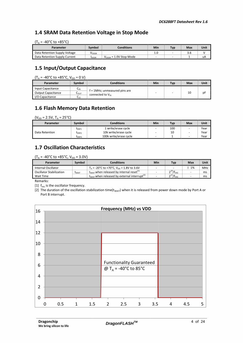
1.7 Oscillation Characteristics
(TA = -40°C to +85°C, VDD = 3.0V)
Parameter Symbol Conditions Min Typ Max Unit
Internal Oscillator TA = -20°C to +70°C, VDD = 1.8V to 3.6V - - ± 1% MHz
Oscillator Stabilization Wait Time
tWAIT tWAIT when released by internal reset[1] - 219/fOSC - ms
tWAIT when released by external interrupt[2] - 213/fOSC - ms
Remarks: [1] fosc is the oscillator frequency. [2] The duration of the oscillation stabilization time(tWAIT) when it is released from power down mode by Port A or
Port B interrupt.
0
2
4
6
8
10
12
14
16
0 0.5 1 1.5 2 2.5 3 3.5 4 4.5 5
Frequency (MHz) vs VDD
Functionality Guaranteed @ TA = -40°C to 85°C

DC6288FT Datasheet Rev 1.6
Dragonchip We bring silicon to life
DragonFLASHTM
5 of 24
1.8 12 bits ADC Characteristics
VDD = 3.3V, VADC ref+ = 3.3V, VADC ref- = 0V
Parameter Symbol Conditions Min Typ Max Unit
Input Voltage Range VADC IN - VSS - VDD V
Voltage Reference Range VADC ref - VSS - VDD V
ADC Voltage Resolution - - 1.61
mV External Voltage Reference (VADC ref+ +VADC ref-) /2048
Output Resolution - Single-ended mode 11
bits Differential mode 12
Conversion Range -
Single-ended mode 0.7 - VDD V
Differential mode (VIN+ - VIN-) - VDD - VDD V Differential Common Mode Voltage
* (Vcm) 0.7 - 1.9 V
Internal Sample & Hold Capacitance
CADC IN - - - 10 pF
Input Resistance RADC IN - 5 - - MΩ
Conversion Clock Frequency fADC VDD = 2.0V – 3.3V 1 - 3.2 MHz
Sampling time tADC_S fADC = 3.2MHz 1 μs
- 3 1/ fADC
Total conversion time tADC_CONV fADC = 3.2MHz 16 μs
- 16 1/ fADC
Dynamic performance
ENOB
VDD = 3.3V, fADC = 3MHz, TA = 25°C
10 - - bits
INL - 1 2 LSB DNL - 1 2 LSB
*Differential Common Mode Voltage = (Vin++Vin-)/2
1.9 Temperature Sensor Characteristics
Parameter Symbol Conditions Min Typ Max Unit
Linearity - ±0.1 - °C
Gain - 2.85 - Digit/°C Offset - 670(Dec) - Digit
1.10 Bandgap Voltage Reference
Parameter Symbol Conditions Min Typ Max Unit
Output Voltage VBG - 1.4 - V
Short-circuit Current IOBG - 2 - mA Load Regulation Load = 0 - 200μA to VSS - 6 - μV/μA
Turn-on Time TBGReady - 50 - μs Supply Rejection Ratio - 1.1 - mV/V
0
1.1
2.2
3.3
0 1.1 2.2 3.3
VIN
+ In
pu
t (V
)
VIN- Input (V)
Full-differential Voltage Conversion Range
0.7 0.5
0.7
0.5
-2048
-1536
-1024
-512
0
512
1024
1536
2048
-3.3 -2.2 -1.1 0 1.1 2.2 3.3
AD
C O
utp
ut
VADC IN (VIN+ - VIN-) (V)
Differential Mode Conversion
Vcm = 1.65V
0
512
1024
1536
2048
0 0.5 1 1.5 2 2.5
AD
C O
utp
ut
VIN+ Input (V)
Single Mode Conversion
VIN- = 0V Vref+= 2.5V
DC6288FT Datasheet Rev 1.6
Dragonchip We bring silicon to life
DragonFLASHTM
6 of 24
1.11 Thermal Characteristics
The maximum junction temperature (TJMAX) can be calculated using the below equation: TJMAX = TAMAX + (PDMAX x θJA) Where:
TAMAX is the maximum ambient temperature in °C
θJA is the package junction-to-ambient thermal resistance in °C/W
PDMAX is the sum of PINTMAX and PIOMAX (PDMAX = PINTMAX + PIOMAX)
PINTMAX is the maximum internal power of the chip. It is calculated as the product of VDD and IDD, expressed in Watts.
PIOMAX is the maximum power dissipation of output pins, where PIOMAX = ∑ (VOL*IOL) + ∑ ((VDD - VOH)*IOH), and taking account of the actual VOL/IOL and VOH/IOH of the IOs at low and high level of the application
Package thermal characteristics is shown in the table below are based on JEDEC JESD51-2 with 4-layer PCB in a natural convection environment. More information about JESD51-2 can be found in www.jedec.org.
Parameter Symbol Parameters Value Unit
Maximum Junction Temperature TJmax +105 °C
Thermal Resistance junction-ambient θJA
TSSOP20 6.5mm x 6.4mm 50
°C/W QFN20 4mm x 4mm 40 QFN24 4mm x 4mm 40
QFN28 4mm x 4mm 40

DC6288FT Datasheet Rev 1.6
Dragonchip We bring silicon to life
DragonFLASHTM
7 of 24
Pin Assignment 2
(TSSOP20 – L)
(TSSOP20 – M)
(TSSOP20 – R)
N.C. N.C.
T24_CA/PWM0/PB4 ECLK/RSTN PC2 REM/PC1 VSS PWM1/PC0 VDD
T24_EX/T24_CC/T0/PA0
20 N.C. 19 N.C. 18 PB1/T1/SL 17 PA7/SCK/T2_CC2 16 PA6/SDI/T2_CC1/RX0* 15 PA5/SDO/T24_OUT/TX0* 14 PA4/T2_CC4/MCLK 13 PA3/T2_CC3 12 PA2/SCK/T2/CNVSTR 11 PA1/SDA/T2EX
1 2 3 4 5 6 7 8 9 10
T24_CA/PWM0/PB4
TX0/PB5 RX0/PB6 ECLK/RSTN PC2 REM/PC1 VSS PWM1/PC0 VDD
T24_EX/T24_CC/T0/PA0
20 PB3/T24_CB 19 PB2 18 PB1/T1/SL 17 PA7/SCK/T2_CC2 16 PA6/SDI/T2_CC1 15 PA5/SDO/T24_OUT 14 PA4/T2_CC4/MCLK 13 PA3/T2_CC3 12 PA2/SCK/T2/CNVSTR 11 PA1/SDA/T2EX
1 2 3 4 5 6 7 8 9 10
PWM1/PC0
T24_CB/PB3 T24_CA/PWM0/PB4 PB5 ECLK/RSTN PC3 PC2 REM/PC1 VSS VDD
20 PB2 19 PB1/T1/SL 18 PB0 17 PA7/SCK/T2_CC2 16 PA6/SDI/T2_CC1 15 PA5/SDO/T24_OUT 14 PA4/T2_CC4/MCLK 13 PA3/T2_CC3 12 PA2/SCK/T2/CNVSTR 11 PA1/SDA/T2EX
1 2 3 4 5 6 7 8 9 10
DC6288FT Datasheet Rev 1.6
Dragonchip We bring silicon to life
DragonFLASHTM
8 of 24
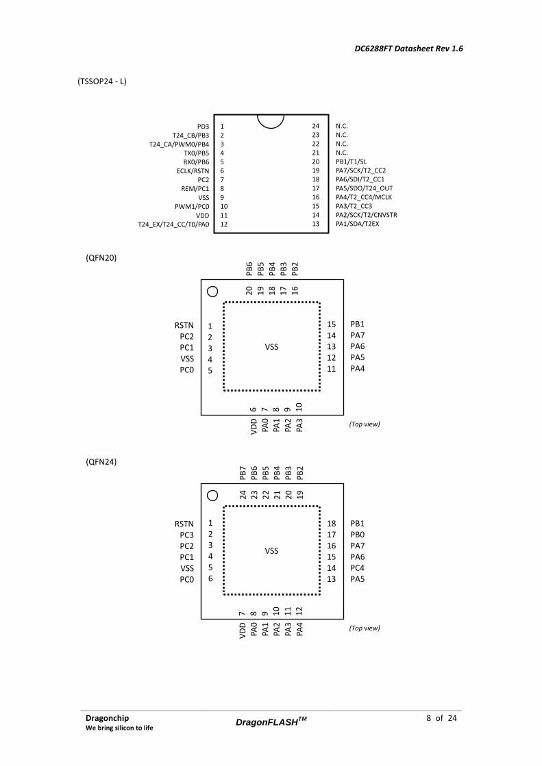
(TSSOP24 - L)
PD3 T24_CB/PB3
T24_CA/PWM0/PB4 TX0/PB5
RX0/PB6 ECLK/RSTN
PC2 REM/PC1 VSS PWM1/PC0 VDD
T24_EX/T24_CC/T0/PA0
24 N.C. 23 N.C. 22 N.C. 21 N.C. 20 PB1/T1/SL 19 PA7/SCK/T2_CC2 18 PA6/SDI/T2_CC1 17 PA5/SDO/T24_OUT 16 PA4/T2_CC4/MCLK 15 PA3/T2_CC3 14 PA2/SCK/T2/CNVSTR 13 PA1/SDA/T2EX
1 2 3 4 5 6 7 8 9 10 11 12
RSTN PC2 PC1 VSS PC0
6
7
8
9
10
VD
D
PA0
PA1
PA2
PA3
VSS
(QFN20)
(Top view)
1 2 3 4 5
PB1 PA7 PA6 PA5 PA4
15 14 13 12 11
20
19
18
17
16
PB
6
PB
5
PB
4
PB
3
PB
2
RSTN PC3
PC2 PC1 VSS PC0
7
8
9
10
11
12
VD
D
PA0
PA1
PA2
PA3
PA4
VSS
(QFN24)
(Top view)
1 2 3 4 5 6
PB1 PB0 PA7 PA6 PC4 PA5
18 17 16 15 14 13
24
23
22
21
20
19
PB
7
PB
6
PB
5
PB
4
PB
3
PB
2

DC6288FT Datasheet Rev 1.6
Dragonchip We bring silicon to life
DragonFLASHTM
9 of 24
Pin Function Timer / PWM Communication Other Analogue (Ch.0/Ch.1)
PA0 Full feature GPIO w/ Interrupt T0/T24EX/T24CC - - ADC V+ / ADC V-
PA1 Full feature GPIO w/ Interrupt T2EX SDA (I2C) - ADC V+ / ADC V-
PA2 Full feature GPIO w/ Interrupt T2/T2OUT SCK (I2C) CNVSTR (ADC) ADC V+ / ADC V-
PA3 Full feature GPIO w/ Interrupt T2CC3 - - ADC V+ / ADC V-
PA4 Full feature GPIO w/ Interrupt T2CC4 - MCLK ADC V+ / ADC V-
PA5 Full feature GPIO w/ Interrupt T24OUT SDO(SPI) / TX(UART0)* - ADC V+ / ADC V-
PA6 Full feature GPIO w/ Interrupt T2CC1 SDI(SPI) / RX(UART0)* - ADC V+ / ADC V-
PA7 Full feature GPIO w/ Interrupt T2CC2 SCK(SPI) - ADC V+ / ADC V-
PB0 Full feature GPIO w/ Interrupt - - - ADC V+ / ADC V-
PB1 Full feature GPIO w/ Interrupt T1 - SL (ISP-SL) ADC V+ / ADC V-
PB2 Full feature GPIO w/ Interrupt - - - ADC V+ / ADC VREF-
PB3 Full feature GPIO w/ Interrupt T24CB - - ADC V+ / ADC V-
PB4 Full feature GPIO w/ Interrupt T24CA/PWM0 - - ADC V+ / ADC V-
PB5 Full feature GPIO w/ Interrupt - TX (UART0) - ADC V+ / ADC V-
PB6 Full feature GPIO w/ Interrupt - RX (UART0) - ADC V+ / ADC V-
PB7 Full feature GPIO w/ Interrupt - - - ADC V+ / ADC V-
PC0 Full feature GPIO w/ Interrupt PWM1 - - ADC VREF+ / ADC V-
PC1 Full feature GPIO w/ Interrupt REM (CA) - - ADC V+ / ADC V-
PC2 Full feature GPIO w/ Interrupt - - - ADC V+ / ADC V-
PC3 Full feature GPIO w/ Interrupt - - - ADC V+ / ADC V-
PC4 Full feature GPIO w/ Interrupt - - - ADC V+ / ADC V-
PD0 Full feature GPIO w/ Interrupt - TX (UART1) - -
PD1 Full feature GPIO w/ Interrupt - RX (UART1) - -
PD2 Full feature GPIO w/ Interrupt - - - -
PD3 Full feature GPIO w/ Interrupt - - - -
*: Available by enabling software setting in DC6288FT (8/16/32) N3L only Pin Function Remarks Other
RSTN External Reset (Active-low) Capacity load must be <50pF ECLK (ISP-SL)
VDD MCU Power Supply Require 100uF + 0.1uF decoupling capacitor -
VSS MCU Power Ground -
PB6 PB7
RSTN PC3
PC2 PC1 VSS
8
9
10
11
12
13
14
PC
0
VD
D
PA0
PD
3
PA1
PA2
PA3
VSS
(QFN28)
(Top view)
1 2 3 4 5 6 7
PA6 PC4 PA5 PD0 PA4 PD1 PD2
21 20 19 18 17 16 15
28
27
26
25
24
23
22
PB
5
PB
4
PB
3
PB
2
PB
1
PB
0
PA7
8051 MCU

DC6288FT Datasheet Rev 1.6
Dragonchip We bring silicon to life
DragonFLASHTM
10 of 24
Architecture Overview 3
DC6288FT is an 8-bit Microcontroller Unit (MCU) with low voltage embedded Flash memory, internal high accuracy RC oscillator, digital peripherals, analogue to digital converter (ADC) and more for general low power or handheld application. As Flash memory is adopted in the MCU, firmware programming and upgrading (In System Programming) can be implemented which can significantly reduce development cycle time and dead inventory. The internal RC oscillator can generate clock signal without any external components, and provide an accurate system clock that is trimmed from factory or by In-system Programmer during MCU programming for a more precise clocking. The MCU also comes with array of timers/counters that can be configured for varies timing or counting needs. There are also capable for generate pulse width modulation signals automatically, allowing system control via analogue means. The built-in communication peripherals provide an automated support for standard protocols used for module to module communication. The 12 bit full differential, or 11 bit single-ended, successive approximation ADC with IO channel multiplexing provides a fast, accurate, and flexible analogue to digital interface for connecting the sensors to the MCU. It supports single, continuous, timer, or external event conversion mode. It also supports window watchdog that allow user program to react to analog event automatically.
Timer 0
T24 Timer
Timer 1 Timer 2
I2C Master/Slave Port Interrupt
8051 1T CPU
Internal 256B SRAM
Expanded 1KB/1.5KB/2KB SRAM
Program & Data Flash
Watchdog Timer
In System Programming
SPI Master
LVD
Digital Part
Analog Part
Full Differential/Single-end ADC
Bandgap Voltage Reference Temperature Sensor
Internal 12 MHz Oscillator
PWM
UART
Internal low frequency Oscillator
POR

DC6288FT Datasheet Rev 1.6
Dragonchip We bring silicon to life
DragonFLASHTM
11 of 24
Central Processing Unit (CPU) 4
The 1T 8051 CPU (Central Processing Unit) is MCS51 instruction compatible. It consists of the instruction decoder, the arithmetic section and the program control section. Each program instruction is decoded by the instruction decoder. This unit generates the internal signals controlling the functions of the individual units within the CPU. They have an effect on the source and destination of data transfers and control the ALU processing. The arithmetic section of the processor performs extensive data manipulation and is comprised of the arithmetic/logic unit (ALU), A register, B register and PSW register. The ALU accepts 8-bit data words from one or two sources and generates an 8-bit result under the control of the instruction decoder. The ALU performs the arithmetic operations add, subtract, multiply, divide, increment, decrement, BDC-decimal-add-adjust and compare, and the logic operations AND, OR, Exclusive OR, complement and rotate (right, left or swap nibble (left four)). Also included is a Boolean processor performing the bit operations as set, clear, complement, jump-if-not-set, jump-if-set-and-clear and move to/from carry. Between any addressable bit (and its complement) and the carry flag, it can perform the bit operations of logical AND or logical OR with the result returned to the carry flag. The program control section controls the sequence in which the instructions stored in program memory are executed. The 16-bit program counter (PC) holds the address of the next instruction to be executed. The conditional branch logic enables internal and external events to the processor to cause a change in the program execution sequence.
Memory 5
Memory comprises of the following elements, namely: 8KB/16KB/32KB Flash memory for Code and Data usage 256B Internal SRAM 1KB/1.5KB/2KB Expanded SRAM 128B Special function register (SFR) 256B External special function register (XFR) The embedded Flash memory can be partitioned for program or data memory use in 512 byte interval. It can be read and write by user program via the built-in Flash controller peripheral. In addition, the write operation is protected by write protection signature to avoid writing accidentally.

DC6288FT Datasheet Rev 1.6
Dragonchip We bring silicon to life
DragonFLASHTM
12 of 24
I/O port 6
There are 4 GPIO ports on the MCU, Port A/B/C/D, and each port have varies number of pins depends on package. The 20-pin TSSOP package has one 8-bit port (PORTA), one 6-bit port (PORTB) and one 3-bit port (PORTC). All ports are latches used to drive the bi-directional I/O lines. The 20-pin QFN package has two 8-bit ports (PA and PB) and one 1-bit port (PORTC). All ports are latches used to drive the bi-directional I/O lines. The 24-pin package has two 8-bit ports (PA and PB) and one 5-bit port (PORTC). All ports are latches used to drive the bi-directional I/O lines. The 28-pin package has two 8-bit ports (PA and PB), one 5-bit port (PORTC), and one 4-bit port (PORTD). All ports are latches used to drive the bi-directional I/O lines. Each individual pin has the following feature that can be configure independently: Digital output mode (High impedance, push-pull, and open-drain mode) Pull-up resistor Input Schmitt trigger Interrupt trigger (Rising, falling, or both edge) Analogue channels

DC6288FT Datasheet Rev 1.6
Dragonchip We bring silicon to life
DragonFLASHTM
13 of 24
12-Bit Full-differential/11-bit Single-end ADC 7
The 12-bit Full-differential/11-bit Single-end ADC module consists of two input paths, V+ and V-, to digitize full differential signal at maximum conversion rate of 200ksps. It can also be configured to measure signal-end input with 11-bit resolution. The start of conversion can be triggered by register, timer overflow or external rising-edge. The reference voltage (VREF) is also selectable from either internal, external or VDD by software configurations.
Internal Bandgap Voltage Reference & Temperature Sensor 8
The internal bandgap voltage reference can provide a fix voltage which can be used for voltage comparison and measurement. The internal temperature sensor uses the ADC to sense the on-chip temperature without external component.

DC6288FT Datasheet Rev 1.6
Dragonchip We bring silicon to life
DragonFLASHTM
14 of 24
General Purpose Timers/Counters 0 & 1 9
Three independent general purpose 16-bit timers/counters, Timer0, and Timer1 are integrated for use in counting events, and causing periodic (repetitive) interrupts. Either can be configured to operate as timer or event counter. In the ‘timer’ function, the registers TLx and/or THx (x = 0, 1) are incremented once every machine cycle. Thus, one can think of it as counting machine cycles. Regarding the ‘counter’ function, the registers TLx and/or THx (x = 0, 1) are incremented in response to a 1-to-0 transition at its corresponding external input pin, T0 or T1. In this function, the external input is sampled during every machine cycle. When the samples show a high in one cycle and a low in the next cycle, the count is incremented. The new count value appears in the register during the cycle following the one in which the transition was detected. Since it takes 2 machine cycles (24 oscillator periods) to recognize a 1-to-0 transition, the maximum count rate is 1/24 of the oscillator frequency. There are no restrictions on the duty cycle of the external input signal, but to ensure that a given level is sampled at least once before it changes, it should be held for at least one full machine cycle.

DC6288FT Datasheet Rev 1.6
Dragonchip We bring silicon to life
DragonFLASHTM
15 of 24
Timer 2 10
Timer 2 consists of a 16-bit timer/counter unit and multiples of compare/capture units. The timer unit itself is capable as a 16-bit system timer/counter, or an external event timer/counter. It also provides the base counter value to the compare/capture units, where each compare/capture unit can act as a system clock timer, external event timer, or PWM output generator.
Timer 24 11
Timer 24 is a 24 bit timer that provides high resolution and counting length designed to capture Infra-red signal carrier frequency as high as 500kHz for event 2 seconds apart. In capture mode, there is 3 capture registers that can time 3 events automatically without servicing. It can also operate as interval timer mode and compare mode which can generates interrupt for timing purposes, and/or pulse width modulation (PWM) outputs.
Timer 2
16 bit Increment
Counter Unit
Compare/Capture Unit 0
Compare/Capture Unit 1
…
Compare/Capture Unit X
T2 Clock Divider
T2/T2EX input
T24 Compare Output Unit

DC6288FT Datasheet Rev 1.6
Dragonchip We bring silicon to life
DragonFLASHTM
16 of 24
Enhanced UART 12
The UART controller is fully compatible with the standard 8051 serial channel with enhancement. The UART perform framing error detection and automatic address recognition in all four modes (one synchronous and three asynchronous. It supports multiprocessor communication as does the standard 80C51 UART.
Inter-Integrated Circuit (I2C) Interface 13
The I2C Bus Controller supports all transfer modes from and to the I
2C bus and transfers up to 100kbit/s
in the standard mode or up to 400kbit/s in the fast mode. The I2C logic handles bytes transfer
autonomously which keeps track of serial transfers, with status registers reflect the status of the I2C Bus
Controller and the I2C bus to applications. The interface also supports the System Management Bus
(SMBus) protocol where additional timeout detection is added.
Serial Peripheral Interface 14
The integrated master mode Serial Peripheral Interface (SPI) controller allows data to be synchronously transmitted and received simultaneously with bit rate up to 4Mbits/s between multiple external peripherals.
Low Voltage Detection Reset 15
The on-chip Low Voltage Detect circuit generates a system reset. It detects the level of VDD by comparing the voltage at pin VDD with reference voltage, VLVD1 (Low Voltage Detect Voltage Level 1). Whenever the voltage at VDD is falling down and passing VLVD1, the IC goes into back-up mode at the moment “VDD = VLVD1”. On the other hand, system reset pulse is generated by the rising slope of VDD. While the voltage at pin VDD is rising up and passing VLVD2 (Low Voltage Detect Voltage Level 2), the reset pulse is occurred at the moment “VDD >= VLVD2“. LVD provides a hysteresis (VLVD2 –VLVD1) to avoid the oscillation near the decision level. For the sake of reducing the current consumption, this function can be disabled when the IC is in power down mode.

DC6288FT Datasheet Rev 1.6
Dragonchip We bring silicon to life
DragonFLASHTM
17 of 24
In System Programming 16
The In System Programming (ISP) feature allows the update of Flash program memory content when the chip is already plugged on the application board. The DC6288FT series support ISP-SL protocol which requires only a 2 wire bus to perform the ISP function, minimize the impact on application design.
Ordering Information 17
Part No Package Program Flash Data Flash SRAM I/O
DC6288FT8N3L DC6288FT8N3M DC6288FT8N3R DC6288FT8Y3L DC6288FT8N6 DC6288FT8Y6 DC6288FT8U6
TSSOP20 TSSOP20 TSSOP20 TSSOP24 QFN20 QFN24 QFN28
8KB Configurable (Program + Data) 8KB Configurable (Program + Data) 8KB Configurable (Program + Data) 8KB Configurable (Program + Data) 8KB Configurable (Program + Data) 8KB Configurable (Program + Data) 8KB Configurable (Program + Data)
256B + 1KB 256B + 1KB 256B + 1KB 256B + 1KB 256B + 1KB 256B + 1KB 256B + 1KB
13 17 17 17 17 21 25
DC6288FT16N3L DC6288FT16N3M DC6288FT16N3R DC6288FT16Y3L DC6288FT16N6 DC6288FT16Y6 DC6288FT16U6
TSSOP20 TSSOP20 TSSOP20 TSSOP24 QFN20 QFN24 QFN28
16KB Configurable (Program + Data) 16KB Configurable (Program + Data) 16KB Configurable (Program + Data) 16KB Configurable (Program + Data) 16KB Configurable (Program + Data) 16KB Configurable (Program + Data) 16KB Configurable (Program + Data)
256B + 1.5KB 256B + 1.5KB 256B + 1.5KB 256B + 1.5KB 256B + 1.5KB 256B + 1.5KB 256B + 1.5KB
13 17 17 17 17 21 25
DC6288FT32N3L DC6288FT32N3M DC6288FT32N3R DC6288FT32Y3L DC6288FT32N6 DC6288FT32Y6 DC6288FT32U6
TSSOP20 TSSOP20 TSSOP20 TSSOP24 QFN20 QFN24 QFN28
32KB Configurable (Program + Data) 32KB Configurable (Program + Data) 32KB Configurable (Program + Data) 32KB Configurable (Program + Data) 32KB Configurable (Program + Data) 32KB Configurable (Program + Data) 32KB Configurable (Program + Data)
256B + 2KB 256B + 2KB 256B + 2KB 256B + 2KB 256B + 2KB 256B + 2KB 256B + 2KB
13 17 17 17 17 21 25

DC6288FT Datasheet Rev 1.6
Dragonchip We bring silicon to life
DragonFLASHTM
18 of 24
Package Outlines 18
18.1 20-pin TSSOP

DC6288FT Datasheet Rev 1.6
Dragonchip We bring silicon to life
DragonFLASHTM
19 of 24
18.2 24-pin TSSOP
Dimensions in millimeters

DC6288FT Datasheet Rev 1.6
Dragonchip We bring silicon to life
DragonFLASHTM
20 of 24
18.3 20-pin QFN

DC6288FT Datasheet Rev 1.6
Dragonchip We bring silicon to life
DragonFLASHTM
21 of 24
18.4 24-pin QFN
DC6288FT Datasheet Rev 1.6
Dragonchip We bring silicon to life
DragonFLASHTM
22 of 24
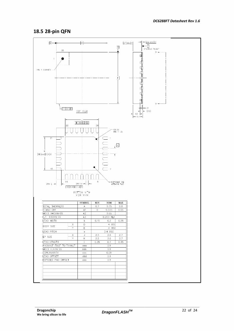
18.5 28-pin QFN

DC6288FT Datasheet Rev 1.6
Dragonchip We bring silicon to life
DragonFLASHTM
23 of 24
Revision History 19
Document Rev No.
Issued Date Section Page Description Edited by Reviewed by
0.6 May, 2016 - - Update to latest design Patrick Li 0.72 Aug, 2017 Combined DC6288FT8/16/32 Patrick Chan
0.9 Feb 2018 Added QFN20 and QFN24 pin assignment Changed 16MHz to 12MHz
Patrick Chan
1.0 Mar 2018 Changed 6688FTxY6 to 6288FTxY6 Patrick Chan 1.1 Mar 2018 Updated QFN24 pin assignment Patrick Chan
1.2 Jun 2018 Updated ADC specification Patrick Li 1.3 Dec 2018 Added QFN28 pin assignment Patrick Chan
1.4 May 2019 Added TSSOP20(L) pin assignment Patrick Chan Danny Ho 1.5 May 2019 Added thermal resistance Patrick Chan
1.6 Aug 2019 Revised package thermal resistance values Added TSSOP24 pin assignment
Patrick Chan

DC6288FT Datasheet Rev 1.6
Dragonchip We bring silicon to life
DragonFLASHTM
24 of 24
Copyright Notice This specification is copyrighted by Dragonchip Ltd. No part of this specification may be reproduced in any form or means, without the expressed written consent Dragonchip Ltd. Disclaimer Dragonchip Ltd. assumes no responsibility for any errors contained herein.
Copyright by Dragonchip Ltd. All Rights Reserved. Dragonchip Ltd. TEL: (852) 2776-0111 FAX: (852) 2776-0996 http://www.dragonchip.com 7