SLOS052D − OCTOBER 1987 − REVISED OCTOBER 2005
1POST OFFICE BOX 655303 • DALLAS, TEXAS 75265
Trimmed Offset Voltage:TLC27L7 . . . 500 µV Max at 25°C, VDD = 5 V
Input Offset Voltage Drift . . . Typically0.1 µV/Month, Including the First 30 Days
Wide Range of Supply Voltages OverSpecified Temperature Range:
0°C to 70°C . . . 3 V to 16 V−40°C to 85°C . . . 4 V to 16 V−55°C to 125°C . . . 4 V to 16 V
Single-Supply Operation
Common-Mode Input Voltage RangeExtends Below the Negative Rail (C-Suffix,I-Suffix Types)
Ultra-Low Power . . . Typically 95 µWat 25°C, VDD = 5 V
Output Voltage Range Includes NegativeRail
High Input Impedance . . . 1012 Ω Typ
ESD-Protection Circuitry
Small-Outline Package Option AlsoAvailable in Tape and Reel
Designed-In Latch-Up immunity
description
The TLC27L2 and TLC27L7 dual operationalamplifiers combine a wide range of input offsetvoltage grades with low offset voltage drift, highinput impedance, extremely low power, and highgain.
AVAILABLE OPTIONS
PACKAGE
TAVIOmaxAT 25°C
SMALLOUTLINE
(D)
CHIPCARRIER
(FK)
CERAMICDIP(JG)
PLASTICDIP(P)
0°C500 µV TLC27L7CD TLC27L7CP
0°C to
500 µV2 mV
TLC27L7CDTLC27L2BCD
— —
TLC27L7CPTLC27L2BCP
to70°C
2 mV5 mV
TLC27L2BCDTLC27L2ACD
— —TLC27L2BCPTLC27L2ACP
70°C5 mV
10 mVTLC27L2ACDTLC27L2CD
TLC27L2ACPTLC27L2CP
−40°C500 µV TLC27L7ID TLC27L7IP
−40°C to
500 µV2 mV
TLC27L7IDTLC27L2BID
— —
TLC27L7IPTLC27L2BIP
to85°C
2 mV5 mV
TLC27L2BIDTLC27L2AID
— —TLC27L2BIPTLC27L2AIP
85°C5 mV
10 mVTLC27L2AIDTLC27L2ID
TLC27L2AIPTLC27L2IP
−55°Cto
500 µVTLC27L7MDTLC27L2MD
TLC27L7MFK TLC27L7MJG TLC27L7MPto
125°C
500 µV10 mV
TLC27L2MDTLC27L2MDRG4
TLC27L7MFKTLC27L2MFK
TLC27L7MJGTLC27L2MJG
TLC27L7MPTLC27L2MP
The D package is available taped and reeled. Add R suffix to the device type(e.g., TLC27L7CDR).
Copyright 2005, Texas Instruments Incorporated !"# $%$ ! ! & ' $$ ()% $ !* $ #) #$* ## !%
LinCMOS is a trademark of Texas Instruments.
−800
Per
cent
age
of U
nits
− %
VIO − Input Offset Voltage − µV
30
8000
−400 0 400
5
10
15
20
25
DISTRIBUTION OF TLC27L7INPUT OFFSET VOLTAGE
1
2
3
4
8
7
6
5
1OUT1IN−1IN+GND
VDD2OUT2IN−2IN+
D, JG, OR P PACKAGE(TOP VIEW)
3 2 1 20 19
9 10 11 12 13
4
5
6
7
8
18
17
16
15
14
NC2OUTNC2IN−NC
NC1IN−
NC1IN+
NC
FK PACKAGE(TOP VIEW)
NC
1OU
TN
C
NC
NC
NC
GN
DN
C
NC − No internal connection
2IN
+D
DV
ÎÎÎÎÎÎÎÎÎÎÎÎÎÎÎÎÎÎÎÎÎÎ
335 Units Tested From 2 Wafer LotsVDD = 5 VTA = 25°CP Package

SLOS052D − OCTOBER 1987 − REVISED OCTOBER 2005
2 POST OFFICE BOX 655303 • DALLAS, TEXAS 75265
description (continued)
These devices use Texas Instruments silicon-gate LinCMOS technology, which provides offset voltagestability far exceeding the stability available with conventional metal-gate processes.
The extremely high input impedance, low bias currents, and low power consumption make these cost-effectivedevices ideal for high gain, low frequency, low power applications. Four offset voltage grades are available(C-suffix and I-suffix types), ranging from the low-cost TLC27L2 (10 mV) to the high-precision TLC27L7(500 µV). These advantages, in combination with good common-mode rejection and supply voltage rejection,make these devices a good choice for new state-of-the-art designs as well as for upgrading existing designs.
In general, many features associated with bipolar technology are available in LinCMOS operational amplifiers,without the power penalties of bipolar technology. General applications such as transducer interfacing, analogcalculations, amplifier blocks, active filters, and signal buffering are easily designed with the TLC27L2 andTLC27L7. The devices also exhibit low voltage single-supply operation and ultra-low power consumption,making them ideally suited for remote and inaccessible battery-powered applications. The common-mode inputvoltage range includes the negative rail.
A wide range of packaging options is available, including small-outline and chip-carrier versions for high-densitysystem applications.
The device inputs and outputs are designed to withstand −100-mA surge currents without sustaining latch-up.
The TLC27L2 and TLC27L7 incorporate internal ESD-protection circuits that prevent functional failures atvoltages up to 2000 V as tested under MIL-STD-883C, Method 3015.2; however, care should be exercised inhandling these devices as exposure to ESD may result in the degradation of the device parametric performance.
The C-Suffix devices are characterized for operation from 0°C to 70°C. The I-suffix devices are characterizedfor operation from −40°C to 85°C. The M-suffix devices are characterized for operation over the full militarytemperature range of −55°C to 125°C.
equivalent schematic (each amplifier)
P5 P6
OUT
N7N6
R7N4
C1R5
N3
GND
N2D2R4D1R3
N1
IN+
IN−
P1
R1
P2
R2 N5
R6
P3 P4
VDD

SLOS052D − OCTOBER 1987 − REVISED OCTOBER 2005
3POST OFFICE BOX 655303 • DALLAS, TEXAS 75265
absolute maximum ratings over operating free-air temperature range (unless otherwise noted) †
Supply voltage, VDD (see Note 1) 18 V. . . . . . . . . . . . . . . . . . . . . . . . . . . . . . . . . . . . . . . . . . . . . . . . . . . . . . . . . . . . Differential input voltage (see Note 2) ±VDD. . . . . . . . . . . . . . . . . . . . . . . . . . . . . . . . . . . . . . . . . . . . . . . . . . . . . . . . Input voltage range, VI (any input) −0.3 V to VDD. . . . . . . . . . . . . . . . . . . . . . . . . . . . . . . . . . . . . . . . . . . . . . . . . . . Input current, II ±5 mA. . . . . . . . . . . . . . . . . . . . . . . . . . . . . . . . . . . . . . . . . . . . . . . . . . . . . . . . . . . . . . . . . . . . . . . . . . Output current, IO (each output) ±30 mA. . . . . . . . . . . . . . . . . . . . . . . . . . . . . . . . . . . . . . . . . . . . . . . . . . . . . . . . . . Total current into VDD 45 mA. . . . . . . . . . . . . . . . . . . . . . . . . . . . . . . . . . . . . . . . . . . . . . . . . . . . . . . . . . . . . . . . . . . . Total current out of GND 45 mA. . . . . . . . . . . . . . . . . . . . . . . . . . . . . . . . . . . . . . . . . . . . . . . . . . . . . . . . . . . . . . . . . . Duration of short-circuit current at (or below) 25°C (see Note 3) Unlimited. . . . . . . . . . . . . . . . . . . . . . . . . . . . . . Continuous total dissipation See Dissipation Rating Table. . . . . . . . . . . . . . . . . . . . . . . . . . . . . . . . . . . . . . . . . . . Operating free-air temperature, TA: C suffix 0°C to 70°C. . . . . . . . . . . . . . . . . . . . . . . . . . . . . . . . . . . . . . . . . . . .
I suffix −40°C to 85°C. . . . . . . . . . . . . . . . . . . . . . . . . . . . . . . . . . . . . . . . . . . M suffix −55°C to 125°C. . . . . . . . . . . . . . . . . . . . . . . . . . . . . . . . . . . . . . . . .
Storage temperature range −65°C to 150°C. . . . . . . . . . . . . . . . . . . . . . . . . . . . . . . . . . . . . . . . . . . . . . . . . . . . . . . Case temperature for 60 seconds: FK package 260°C. . . . . . . . . . . . . . . . . . . . . . . . . . . . . . . . . . . . . . . . . . . . . . Lead temperature 1,6 mm (1/16 inch) from case for 10 seconds: D or P package 260°C. . . . . . . . . . . . . . . . . Lead temperature 1,6 mm (1/16 inch) from case for 60 seconds: JG package 300°C. . . . . . . . . . . . . . . . . . . .
† Stresses beyond those listed under “absolute maximum ratings” may cause permanent damage to the device. These are stress ratings only, andfunctional operation of the device at these or any other conditions beyond those indicated under “recommended operating conditions” is notimplied. Exposure to absolute-maximum-rated conditions for extended periods may affect device reliability.
NOTES: 1. All voltage values, except differential voltages, are with respect to network ground.2. Differential voltages are at IN+ with respect to IN−.3. The output may be shorted to either supply. Temperature and/or supply voltages must be limited to ensure that the maximum
dissipation rating is not exceeded (see application section).
DISSIPATION RATING TABLE
PACKAGETA ≤ 25°C DERATING FACTOR TA = 70°C TA = 85°C TA = 125°C
PACKAGETA ≤ 25 C
POWER RATINGDERATING FACTORABOVE TA = 25°C
TA = 70 CPOWER RATING
TA = 85 CPOWER RATING
TA = 125 CPOWER RATING
D 725 mW 5.8 mW/°C 464 mW 377 mW —
FK 1375 mW 11 mW/°C 880 mW 715 mW 275 mW
JG 1050 mW 8.4 mW/°C 672 mW 546 mW 210 mW
P 1000 mW 8 mW/°C 640 mW 520 mW —
recommended operating conditions
C SUFFIX I SUFFIX M SUFFIXUNIT
MIN MAX MIN MAX MIN MAXUNIT
Supply voltage, VDD 3 16 4 16 4 16 V
Common-mode input voltage, VICVDD = 5 V −0.2 3.5 −0.2 3.5 0 3.5
VCommon-mode input voltage, VIC VDD = 10 V −0.2 8.5 −0.2 8.5 0 8.5V
Operating free-air temperature, TA 0 70 −40 85 −55 125 °C

SLOS052D − OCTOBER 1987 − REVISED OCTOBER 2005
4 POST OFFICE BOX 655303 • DALLAS, TEXAS 75265
electrical characteristics at specified free-air temperature, V DD = 5 V (unless otherwise noted)
PARAMETER TEST CONDITIONS TA†
TLC27L2CTLC27L2ACTLC27L2BCTLC27L7C
UNIT
MIN TYP MAX
TLC27L2CVO = 1.4 V, VIC = 0, 25°C 1.1 10
TLC27L2CVO = 1.4 V,RS = 50 Ω,
VIC = 0,RL = 1 MΩ Full range 12
mV
TLC27L2ACVO = 1.4 V, VIC = 0, 25°C 0.9 5
mV
VIO Input offset voltage
TLC27L2ACVO = 1.4 V,RS = 50 Ω,
VIC = 0,RL = 1 MΩ Full range 6.5
VIO Input offset voltage
TLC27L2BCVO = 1.4 V, VIC = 0, 25°C 204 2000
TLC27L2BCVO = 1.4 V,RS = 50 Ω,
VIC = 0,RL = 1 MΩ Full range 3000
V
TLC27L7CVO = 1.4 V, VIC = 0, 25°C 170 500
µV
TLC27L7CVO = 1.4 V,RS = 50 Ω,
VIC = 0,RL = 1 MΩ Full range 1500
VIOAverage temperature coefficient of input 25°C to
1.1 V/°CαVIOAverage temperature coefficient of inputoffset voltage
25 C to70°C 1.1 µV/°C
IIO Input offset current (see Note 4) VO = 2.5 V, VIC = 2.5 V25°C 0.1 60
pAIIO Input offset current (see Note 4) VO = 2.5 V, VIC = 2.5 V70°C 7 300
pA
IIB Input bias current (see Note 4) VO = 2.5 V, VIC = 2.5 V25°C 0.6 60
pAIIB Input bias current (see Note 4) VO = 2.5 V, VIC = 2.5 V70°C 50 600
pA
−0.2 −0.325°C
−0.2to
−0.3to V
VICRCommon-mode input voltage range
25 C to4
to4.2
V
VICRCommon-mode input voltage range(see Note 5) −0.2(see Note 5)
Full range−0.2
to VFull range to3.5
V
25°C 3.2 4.1
VOH High-level output voltage VID = 100 mV, RL = 1 MΩ 0°C 3 4.1 VVOH High-level output voltage VID = 100 mV, RL = 1 MΩ70°C 3 4.2
V
25°C 0 50
VOL Low-level output voltage VID = −100 mV, IOL = 0 0°C 0 50 mVVOL Low-level output voltage VID = −100 mV, IOL = 0
70°C 0 50
mV
Large-signal differential voltage25°C 50 700
AVDLarge-signal differential voltageamplification VO = 0.25 V to 2 V, RL = 1 MΩ 0°C 50 700 V/mVAVD amplification VO = 0.25 V to 2 V, RL = 1 MΩ
70°C 50 380
V/mV
25°C 65 94
CMRR Common-mode rejection ratio VIC = VICRmin 0°C 60 95 dBCMRR Common-mode rejection ratio VIC = VICRmin
70°C 60 95
dB
Supply-voltage rejection ratio25°C 70 97
kSVRSupply-voltage rejection ratio(∆VDD/∆VIO) VDD = 5 V to 10 V, VO = 1.4 V 0°C 60 97 dBkSVR (∆VDD/∆VIO) VDD = 5 V to 10 V, VO = 1.4 V
70°C 60 98
dB
VO = 2.5 V, VIC = 2.5 V,25°C 20 34
IDD Supply current (two amplifiers)VO = 2.5 V,No load
VIC = 2.5 V,0°C 24 42 µAIDD Supply current (two amplifiers)
No load70°C 16 28
µA
† Full range is 0°C to 70°C.NOTES: 4. The typical values of input bias current and input offset current below 5 pA were determined mathematically.
5. This range also applies to each input individually.
SLOS052D − OCTOBER 1987 − REVISED OCTOBER 2005
5POST OFFICE BOX 655303 • DALLAS, TEXAS 75265
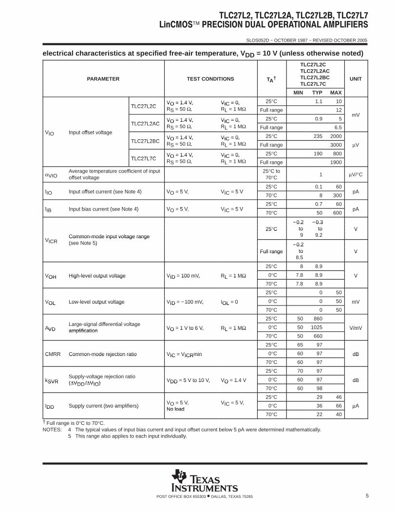
electrical characteristics at specified free-air temperature, V DD = 10 V (unless otherwise noted)
PARAMETER TEST CONDITIONS TA†
TLC27L2CTLC27L2ACTLC27L2BCTLC27L7C
UNIT
MIN TYP MAX
TLC27L2CVO = 1.4 V, VIC = 0, 25°C 1.1 10
TLC27L2CVO = 1.4 V,RS = 50 Ω,
VIC = 0,RL = 1 MΩ Full range 12
mV
TLC27L2ACVO = 1.4 V, VIC = 0, 25°C 0.9 5
mV
VIO Input offset voltage
TLC27L2ACVO = 1.4 V,RS = 50 Ω,
VIC = 0,RL = 1 MΩ Full range 6.5
VIO Input offset voltage
TLC27L2BCVO = 1.4 V, VIC = 0, 25°C 235 2000
TLC27L2BCVO = 1.4 V,RS = 50 Ω,
VIC = 0,RL = 1 MΩ Full range 3000 µV
TLC27L7CVO = 1.4 V, VIC = 0, 25°C 190 800
TLC27L7CVO = 1.4 V,RS = 50 Ω,
VIC = 0,RL = 1 MΩ Full range 1900
αVIOAverage temperature coefficient of inputoffset voltage
25°C to70°C 1 µV/°C
IIO Input offset current (see Note 4) VO = 5 V, VIC = 5 V25°C 0.1 60
pAIIO Input offset current (see Note 4) VO = 5 V, VIC = 5 V70°C 8 300
pA
IIB Input bias current (see Note 4) VO = 5 V, VIC = 5 V25°C 0.7 60
pAIIB Input bias current (see Note 4) VO = 5 V, VIC = 5 V70°C 50 600
pA
−0.2 −0.325°C
−0.2to
−0.3to V
VICRCommon-mode input voltage range
25 C to9
to9.2
V
VICRCommon-mode input voltage range(see Note 5) −0.2(see Note 5)
Full range−0.2
to VFull range to8.5
V
25°C 8 8.9
VOH High-level output voltage VID = 100 mV, RL = 1 MΩ 0°C 7.8 8.9 VVOH High-level output voltage VID = 100 mV, RL = 1 MΩ70°C 7.8 8.9
V
25°C 0 50
VOL Low-level output voltage VID = −100 mV, IOL = 0 0°C 0 50 mVVOL Low-level output voltage VID = −100 mV, IOL = 0
70°C 0 50
mV
Large-signal differential voltage25°C 50 860
AVDLarge-signal differential voltageamplification VO = 1 V to 6 V, RL = 1 MΩ 0°C 50 1025 V/mVAVD amplification VO = 1 V to 6 V, RL = 1 MΩ
70°C 50 660
V/mV
25°C 65 97
CMRR Common-mode rejection ratio VIC = VICRmin 0°C 60 97 dBCMRR Common-mode rejection ratio VIC = VICRmin
70°C 60 97
dB
Supply-voltage rejection ratio25°C 70 97
kSVRSupply-voltage rejection ratio(∆VDD/∆VIO) VDD = 5 V to 10 V, VO = 1.4 V 0°C 60 97 dBkSVR (∆VDD/∆VIO) VDD = 5 V to 10 V, VO = 1.4 V
70°C 60 98
dB
VO = 5 V, VIC = 5 V, 25°C 29 46
IDD Supply current (two amplifiers)VO = 5 V,No load
VIC = 5 V, 0°C 36 66 µAIDD Supply current (two amplifiers)
No load70°C 22 40
µA
† Full range is 0°C to 70°C.NOTES: 4 The typical values of input bias current and input offset current below 5 pA were determined mathematically.
5 This range also applies to each input individually.

SLOS052D − OCTOBER 1987 − REVISED OCTOBER 2005
6 POST OFFICE BOX 655303 • DALLAS, TEXAS 75265
electrical characteristics at specified free-air temperature, V DD = 5 V (unless otherwise noted)
PARAMETER TEST CONDITIONS TA†
TLC27L2ITLC27L2AITLC27L2BITLC27L7I
UNIT
MIN TYP MAX
TLC27L2IVO = 1.4 V, VIC = 0, 25°C 1.1 10
TLC27L2IVO = 1.4 V,RS = 50 Ω,
VIC = 0,RL = 1 MΩ Full range 13
mV
TLC27L2AIVO = 1.4 V, VIC = 0, 25°C 0.9 5
mV
VIO Input offset voltage
TLC27L2AIVO = 1.4 V,RS = 50 Ω,
VIC = 0,RL = 1 MΩ Full range 7
VIO Input offset voltage
TLC27L2BIVO = 1.4 V, VIC = 0, 25°C 240 2000
TLC27L2BIVO = 1.4 V,RS = 50 Ω,
VIC = 0,RL = 1 MΩ Full range 3500
V
TLC27L7IVO = 1.4 V, VIC = 0, 25°C 170 500
µV
TLC27L7IVO = 1.4 V,RS = 50 Ω,
VIC = 0,RL = 1 MΩ Full range 2000
VIOAverage temperature coefficient of 25°C to
1.1 V/°CαVIOAverage temperature coefficient ofinput offset voltage
25 C to85°C 1.1 µV/°C
IIO Input offset current (see Note 4) VO = 2.5 V, VIC = 2.5 V25°C 0.1 60
pAIIO Input offset current (see Note 4) VO = 2.5 V, VIC = 2.5 V85°C 24 1000
pA
IIB Input bias current (see Note 4) VO = 2.5 V, VIC = 2.5 V25°C 0.6 60
pAIIB Input bias current (see Note 4) VO = 2.5 V, VIC = 2.5 V85°C 200 2000
pA
−0.2 −0.325°C
−0.2to
−0.3to V
VICRCommon-mode input voltage range
25 C to4
to4.2
V
VICRCommon-mode input voltage range(see Note 5) −0.2(see Note 5)
Full range−0.2
to VFull range to3.5
V
25°C 3.2 4.1
VOH High-level output voltage VID = 100 mV, RL = 1 MΩ −40°C 3 4.1 VVOH High-level output voltage VID = 100 mV, RL = 1 MΩ85°C 3 4.2
V
25°C 0 50
VOL Low-level output voltage VID = −100 mV, IOL = 0 −40°C 0 50 mVVOL Low-level output voltage VID = −100 mV, IOL = 0
85°C 0 50
mV
Large-signal differential25°C 50 480
AVDLarge-signal differentialvoltage amplification VO = 0.25 V to 2 V, RL = 1 MΩ −40°C 50 900 V/mVAVD voltage amplification VO = 0.25 V to 2 V, RL = 1 MΩ
85°C 50 330
V/mV
25°C 65 94
CMRR Common-mode rejection ratio VIC = VICRmin −40°C 60 95 dBCMRR Common-mode rejection ratio VIC = VICRmin
85°C 60 95
dB
Supply-voltage rejection ratio25°C 70 97
kSVRSupply-voltage rejection ratio(∆VDD/∆VIO) VDD = 5 V to 10 V, VO = 1.4 V −40°C 60 97 dBkSVR (∆VDD/∆VIO) VDD = 5 V to 10 V, VO = 1.4 V
85°C 60 98
dB
VO = 2.5 V, VIC = 2.5 V, 25°C 20 34
IDD Supply current (two amplifiers)VO = 2.5 V,No load
VIC = 2.5 V, −40°C 31 54 µAIDD Supply current (two amplifiers)
No load85°C 15 26
µA
† Full range is −40°C to 85°C.NOTES: 4. The typical values of input bias current and input offset current below 5 pA were determined mathematically.
5. This range also applies to each input individually.
SLOS052D − OCTOBER 1987 − REVISED OCTOBER 2005
7POST OFFICE BOX 655303 • DALLAS, TEXAS 75265
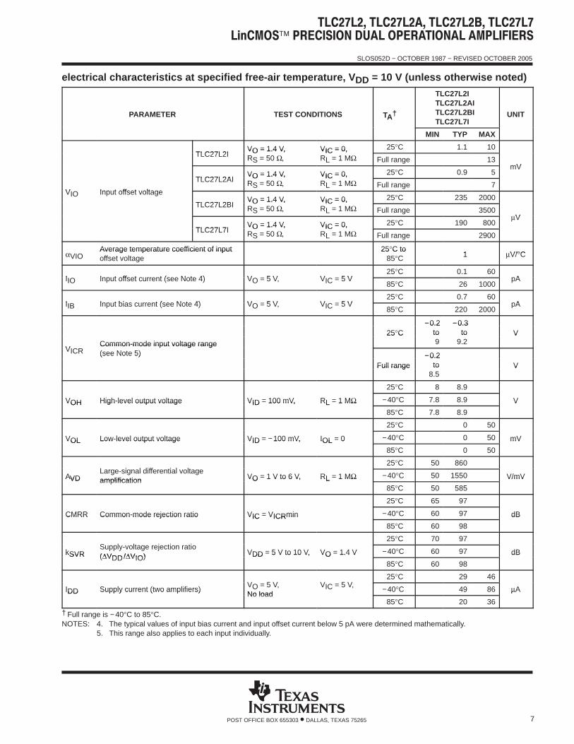
electrical characteristics at specified free-air temperature, V DD = 10 V (unless otherwise noted)
PARAMETER TEST CONDITIONS TA†
TLC27L2ITLC27L2AITLC27L2BITLC27L7I
UNIT
MIN TYP MAX
TLC27L2IVO = 1.4 V, VIC = 0, 25°C 1.1 10
TLC27L2IVO = 1.4 V,RS = 50 Ω,
VIC = 0,RL = 1 MΩ Full range 13
mV
TLC27L2AIVO = 1.4 V, VIC = 0, 25°C 0.9 5
mV
VIO Input offset voltage
TLC27L2AIVO = 1.4 V,RS = 50 Ω,
VIC = 0,RL = 1 MΩ Full range 7
VIO Input offset voltage
TLC27L2BIVO = 1.4 V, VIC = 0, 25°C 235 2000
TLC27L2BIVO = 1.4 V,RS = 50 Ω,
VIC = 0,RL = 1 MΩ Full range 3500
V
TLC27L7IVO = 1.4 V, VIC = 0, 25°C 190 800
µV
TLC27L7IVO = 1.4 V,RS = 50 Ω,
VIC = 0,RL = 1 MΩ Full range 2900
VIOAverage temperature coefficient of input 25°C to
1 V/°CαVIOAverage temperature coefficient of inputoffset voltage
25 C to85°C 1 µV/°C
IIO Input offset current (see Note 4) VO = 5 V, VIC = 5 V25°C 0.1 60
pAIIO Input offset current (see Note 4) VO = 5 V, VIC = 5 V85°C 26 1000
pA
IIB Input bias current (see Note 4) VO = 5 V, VIC = 5 V25°C 0.7 60
pAIIB Input bias current (see Note 4) VO = 5 V, VIC = 5 V85°C 220 2000
pA
−0.2 −0.325°C
−0.2to
−0.3to V
VICRCommon-mode input voltage range
25 C to9
to9.2
V
VICRCommon-mode input voltage range(see Note 5) −0.2(see Note 5)
Full range−0.2
to VFull range to8.5
V
25°C 8 8.9
VOH High-level output voltage VID = 100 mV, RL = 1 MΩ −40°C 7.8 8.9 VVOH High-level output voltage VID = 100 mV, RL = 1 MΩ85°C 7.8 8.9
V
25°C 0 50
VOL Low-level output voltage VID = −100 mV, IOL = 0 −40°C 0 50 mVVOL Low-level output voltage VID = −100 mV, IOL = 0
85°C 0 50
mV
Large-signal differential voltage25°C 50 860
AVDLarge-signal differential voltageamplification VO = 1 V to 6 V, RL = 1 MΩ −40°C 50 1550 V/mVAVD amplification VO = 1 V to 6 V, RL = 1 MΩ
85°C 50 585
V/mV
25°C 65 97
CMRR Common-mode rejection ratio VIC = VICRmin −40°C 60 97 dBCMRR Common-mode rejection ratio VIC = VICRmin
85°C 60 98
dB
Supply-voltage rejection ratio25°C 70 97
kSVRSupply-voltage rejection ratio(∆VDD/∆VIO) VDD = 5 V to 10 V, VO = 1.4 V −40°C 60 97 dBkSVR (∆VDD/∆VIO) VDD = 5 V to 10 V, VO = 1.4 V
85°C 60 98
dB
VO = 5 V, VIC = 5 V, 25°C 29 46
IDD Supply current (two amplifiers)VO = 5 V,No load
VIC = 5 V, −40°C 49 86 µAIDD Supply current (two amplifiers)
No load85°C 20 36
µA
† Full range is −40°C to 85°C.NOTES: 4. The typical values of input bias current and input offset current below 5 pA were determined mathematically.
5. This range also applies to each input individually.

SLOS052D − OCTOBER 1987 − REVISED OCTOBER 2005
8 POST OFFICE BOX 655303 • DALLAS, TEXAS 75265
electrical characteristics at specified free-air temperature, V DD = 5 V (unless otherwise noted)
PARAMETER TEST CONDITIONS TA†TLC27L2MTLC27L7M UNITPARAMETER TEST CONDITIONS TA†
MIN TYP MAXUNIT
TLC27L2MVO = 1.4 V, VIC = 0, 25°C 1.1 10
mV
VIO Input offset voltage
TLC27L2MVO = 1.4 V,RS = 50 Ω,
VIC = 0,RL = 1 MΩ Full range 12
mV
VIO Input offset voltage
TLC27L7MVO = 1.4 V, VIC = 0, 25°C 170 500
µVTLC27L7MVO = 1.4 V,RS = 50 Ω,
VIC = 0,RL = 1 MΩ Full range 3750
µV
αVIOAverage temperature coefficient of 25°C to
1.4 µV/°CαVIOAverage temperature coefficient ofinput offset voltage
25 C to125°C 1.4 µV/°C
IIO Input offset current (see Note 4) VO = 2.5 V, VIC = 2.5 V25°C 0.1 60 pA
IIO Input offset current (see Note 4) VO = 2.5 V, VIC = 2.5 V125°C 1.4 15 nA
IIB Input bias current (see Note 4) VO = 2.5 V, VIC = 2.5 V25°C 0.6 60 pA
IIB Input bias current (see Note 4) VO = 2.5 V, VIC = 2.5 V125°C 9 35 nA
0 −0.325°C
0to
−0.3to V
VICRCommon-mode input voltage range
25 C to4
to4.2
V
VICRCommon-mode input voltage range(see Note 5) 0(see Note 5)
Full range0to VFull range to
3.5V
25°C 3.2 4.1
VOH High-level output voltage VID = 100 mV, RL = 1 MΩ −55°C 3 4.1 VVOH High-level output voltage VID = 100 mV, RL = 1 MΩ125°C 3 4.2
V
25°C 0 50
VOL Low-level output voltage VID = −100 mV, IOL = 0 −55°C 0 50 mVVOL Low-level output voltage VID = −100 mV, IOL = 0125°C 0 50
mV
Large-signal differential voltage25°C 50 500
AVDLarge-signal differential voltageamplification VO = 0.25 V to 2 V, RL = 1 MΩ −55°C 25 1000 V/mVAVD amplification VO = 0.25 V to 2 V, RL = 1 MΩ
125°C 25 200V/mV
25°C 65 94
CMRR Common-mode rejection ratio VIC = VICRmin −55°C 60 95 dBCMRR Common-mode rejection ratio VIC = VICRmin125°C 60 85
dB
Supply-voltage rejection ratio25°C 70 97
kSVRSupply-voltage rejection ratio(∆VDD/∆VIO) VDD = 5 V to 10 V, VO = 1.4 V −55°C 60 97 dBkSVR (∆VDD/∆VIO) VDD = 5 V to 10 V, VO = 1.4 V
125°C 60 98dB
VO = 2.5 V, VIC = 2.5 V, 25°C 20 34
IDD Supply current (two amplifiers)VO = 2.5 V,No load
VIC = 2.5 V, −55°C 35 60 µAIDD Supply current (two amplifiers)
No load125°C 14 24
µA
† Full range is −55°C to 125°C.NOTES: 4. The typical values of input bias current and input offset current below 5 pA were determined mathematically.
5. This range also applies to each input individually.

SLOS052D − OCTOBER 1987 − REVISED OCTOBER 2005
9POST OFFICE BOX 655303 • DALLAS, TEXAS 75265
electrical characteristics at specified free-air temperature, V DD = 10 V (unless otherwise noted)
PARAMETER TEST CONDITIONS TA†TLC27L2MTLC27L7M UNITPARAMETER TEST CONDITIONS TA†
MIN TYP MAXUNIT
TLC27L2MVO = 1.4 V, VIC = 0, 25°C 1.1 10
mV
VIO Input offset voltage
TLC27L2MVO = 1.4 V,RS = 50 Ω,
VIC = 0,RL = 1 MΩ Full range 12
mV
VIO Input offset voltage
TLC27L7MVO = 1.4 V, VIC = 0, 25°C 190 800
µVTLC27L7MVO = 1.4 V,RS = 50 Ω,
VIC = 0,RL = 1 MΩ Full range 4300
µV
αVIOAverage temperature coefficient of 25°C to
1.4 µV/°CαVIOAverage temperature coefficient ofinput offset voltage
25 C to125°C
1.4 µV/°C
IIO Input offset current (see Note 4) VO = 5 V, VIC = 5 V25°C 0.1 60 pA
IIO Input offset current (see Note 4) VO = 5 V, VIC = 5 V125°C 1.8 15 nA
IIB Input bias current (see Note 4) VO = 5 V, VIC = 5 V25°C 0.7 60 pA
IIB Input bias current (see Note 4) VO = 5 V, VIC = 5 V125°C 10 35 nA
0 −0.325°C
0to
−0.3to V
VICRCommon-mode input voltage range
25 C to9
to9.2
V
VICRCommon-mode input voltage range(see Note 5) 0(see Note 5)
Full range0to VFull range to
8.5V
25°C 8 8.9
VOH High-level output voltage VID = 100 mV, RL = 1 MΩ −55°C 7.8 8.8 VVOH High-level output voltage VID = 100 mV, RL = 1 MΩ125°C 7.8 9
V
25°C 0 50
VOL Low-level output voltage VID = −100 mV, IOL = 0 −55°C 0 50 mVVOL Low-level output voltage VID = −100 mV, IOL = 0125°C 0 50
mV
Large-signal differential voltage25°C 50 860
AVDLarge-signal differential voltageamplification
VO = 1 V to 6 V, RL = 1 MΩ −55°C 25 1750 V/mVAVD amplification VO = 1 V to 6 V, RL = 1 MΩ125°C 25 380
V/mV
25°C 65 97
CMRR Common-mode rejection ratio VIC = VICRmin −55°C 60 97 dBCMRR Common-mode rejection ratio VIC = VICRmin125°C 60 91
dB
Supply-voltage rejection ratio25°C 70 97
kSVRSupply-voltage rejection ratio(∆VDD/∆VIO)
VDD = 5 V to 10 V, VO = 1.4 V −55°C 60 97 dBkSVR (∆VDD/∆VIO) VDD = 5 V to 10 V, VO = 1.4 V125°C 60 98
dB
VO = 5 V, VIC = 5 V, 25°C 29 46
IDD Supply current (two amplifiers)VO = 5 V,No load
VIC = 5 V, −55°C 56 96 µAIDD Supply current (two amplifiers)
No load125°C 18 30
µA
† Full range is −55 °C to 125°C.NOTES: 4. The typical values of input bias current and input offset current below 5 pA were determined mathematically.
5. This range also applies to each input individually.
SLOS052D − OCTOBER 1987 − REVISED OCTOBER 2005
10 POST OFFICE BOX 655303 • DALLAS, TEXAS 75265
operating characteristics, V DD = 5 V
PARAMETER TEST CONDITIONS TA
TLC27L2CTLC27L2ACTLC27L2BCTLC27L7C
UNIT
MIN TYP MAX
25°C 0.03
R = 1 M ,VI(PP) = 1 V 0°C 0.04
SR Slew rate at unity gainRL = 1 MΩ,CL = 20 pF,
VI(PP) = 1 V
70°C 0.03V/ sSR Slew rate at unity gain
LCL = 20 pF,See Figure 1 25°C 0.03
V/µsSee Figure 1
VI(PP) = 2.5 V 0°C 0.03VI(PP) = 2.5 V
70°C 0.02
Vn Equivalent input noise voltagef = 1 kHz, RS = 20 Ω,
25°C 68 nV/√HzVn Equivalent input noise voltagef = 1 kHz,See Figure 2
RS = 20 Ω,25°C 68 nV/√Hz
VO = VOH, CL = 20 pF,25°C 5
BOM Maximum output-swing bandwidthVO = VOH,RL = 1 MΩ,
CL = 20 pF,See Figure 1
0°C 6 kHzBOM Maximum output-swing bandwidth RL = 1 MΩ, See Figure 170°C 4.5
kHz
VI = 10 mV, CL = 20 pF,25°C 85
B1 Unity-gain bandwidthVI = 10 mV,See Figure 3
CL = 20 pF,0°C 100 kHzB1 Unity-gain bandwidth See Figure 3
70°C 65
kHz
VI = 10 mV, f = B1,25°C 34°
φm Phase marginVI = 10 mV,CL = 20 pF,
f = B1,See Figure 3
0°C 36°φm Phase marginCL = 20 pF, See Figure 3
70°C 30°
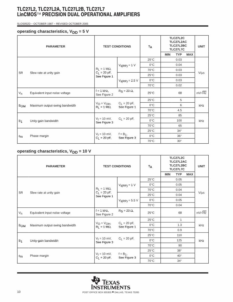
operating characteristics, V DD = 10 V
PARAMETER TEST CONDITIONS TA
TLC27L2CTLC27L2ACTLC27L2BCTLC27L7C
UNIT
MIN TYP MAX
25°C 0.05
R = 1 M ,VI(PP) = 1 V 0°C 0.05
SR Slew rate at unity gainRL = 1 MΩ,CL = 20 pF,
VI(PP) = 1 V
70°C 0.04V/ sSR Slew rate at unity gain
LCL = 20 pF,See Figure 1 25°C 0.04
V/µsSee Figure 1
VI(PP) = 5.5 V 0°C 0.05VI(PP) = 5.5 V
70°C 0.04
Vn Equivalent input noise voltagef = 1 kHz, RS = 20 Ω,
25°C 68 nV/√HzVn Equivalent input noise voltagef = 1 kHz,See Figure 2
RS = 20 Ω,25°C 68 nV/√Hz
VO = VOH, CL = 20 pF,25°C 1
BOM Maximum output-swing bandwidthVO = VOH,RL = 1 MΩ,
CL = 20 pF,See Figure 1
0°C 1.3 kHzBOM Maximum output-swing bandwidth RL = 1 MΩ, See Figure 170°C 0.9
kHz
VI = 10 mV, CL = 20 pF,25°C 110
B1 Unity-gain bandwidthVI = 10 mV,See Figure 3
CL = 20 pF,0°C 125 kHzB1 Unity-gain bandwidth See Figure 3
70°C 90
kHz
VI = 10 mV, f = B1,25°C 38°
φm Phase marginVI = 10 mV,CL = 20 pF,
f = B1,See Figure 3
0°C 40°φm Phase marginCL = 20 pF, See Figure 3
70°C 34°

SLOS052D − OCTOBER 1987 − REVISED OCTOBER 2005
11POST OFFICE BOX 655303 • DALLAS, TEXAS 75265
operating characteristics, V DD = 5 V
PARAMETER TEST CONDITIONS TA
TLC27L2ITLC27L2AITLC27L2BITLC27L7I
UNIT
MIN TYP MAX
25°C 0.03
R = 1 M ,VI(PP) = 1 V −40°C 0.04
SR Slew rate at unity gainRL = 1 MΩ,CL = 20 pF,
VI(PP) = 1 V
85°C 0.03V/ sSR Slew rate at unity gain
LCL = 20 pF,See Figure 1 25°C 0.03
V/µsSee Figure 1
VI(PP) = 2.5 V −40°C 0.04VI(PP) = 2.5 V
85°C 0.02
Vn Equivalent input noise voltagef = 1 kHz, RS = 20 Ω,
25°C 68 nV/√HzVn Equivalent input noise voltagef = 1 kHz,See Figure 2
RS = 20 Ω,25°C 68 nV/√Hz
VO = VOH, CL = 20 pF,25°C 5
BOM Maximum output-swing bandwidthVO = VOH,RL = 1 MΩ,
CL = 20 pF,See Figure 1
−40°C 7 kHzBOM Maximum output-swing bandwidth RL = 1 MΩ, See Figure 185°C 4
kHz
VI = 10 mV, CL = 20 pF,25°C 85
B1 Unity-gain bandwidthVI = 10 mV,See Figure 3
CL = 20 pF,−40°C 130 kHzB1 Unity-gain bandwidth See Figure 3
85°C 55
kHz
VI = 10 mV, f = B1,25°C 34°
φm Phase marginVI = 10 mV,CL = 20 pF,
f = B1,See Figure 3
−40°C 38°φm Phase marginCL = 20 pF, See Figure 3
85°C 29°
operating characteristics, V DD = 10 V
PARAMETER TEST CONDITIONS TA
TLC27L2ITLC27L2AITLC27L2BITLC27L7I
UNIT
MIN TYP MAX
25°C 0.05
R = 1 M ,VI(PP) = 1 V −40°C 0.06
SR Slew rate at unity gainRL = 1 MΩ,CL = 20 pF,
VI(PP) = 1 V
85°C 0.03V/ sSR Slew rate at unity gain
LCL = 20 pF,See Figure 1 25°C 0.04
V/µsSee Figure 1
VI(PP) = 5.5 V −40°C 0.05VI(PP) = 5.5 V
85°C 0.03
Vn Equivalent input noise voltagef = 1 kHz, RS = 20 Ω,
25°C 68 nV/√HzVn Equivalent input noise voltagef = 1 kHz,See Figure 2
RS = 20 Ω,25°C 68 nV/√Hz
VO = VOH, CL = 20 pF,25°C 1
BOM Maximum output-swing bandwidthVO = VOH,RL = 1 MΩ,
CL = 20 pF,See Figure 1
−40°C 1.4 kHzBOM Maximum output-swing bandwidth RL = 1 MΩ, See Figure 185°C 0.8
kHz
VI = 10 mV, CL = 20 pF,25°C 110
B1 Unity-gain bandwidthVI = 10 mV,See Figure 3
CL = 20 pF,−40°C 155 kHzB1 Unity-gain bandwidth See Figure 3
85°C 80
kHz
VI = 10 mV, f = B1,25°C 38°
φm Phase marginVI = 10 mV,CL = 20 pF,
f = B1,See Figure 3
−40°C 42°φm Phase marginCL = 20 pF, See Figure 3
85°C 32°
SLOS052D − OCTOBER 1987 − REVISED OCTOBER 2005
12 POST OFFICE BOX 655303 • DALLAS, TEXAS 75265
operating characteristics, V DD = 5 V
PARAMETER TEST CONDITIONS TA
TLC27L2MTLC27L7M UNITPARAMETER TEST CONDITIONS TA
MIN TYP MAXUNIT
25°C 0.03
R = 1 M ,VI(PP) = 1 V −55°C 0.04
SR Slew rate at unity gainRL = 1 MΩ,CL = 20 pF,
VI(PP) = 1 V
125°C 0.02V/ sSR Slew rate at unity gain
LCL = 20 pF,See Figure 1 25°C 0.03
V/µsSee Figure 1
VI(PP) = 2.5 V −55°C 0.04VI(PP) = 2.5 V
125°C 0.02
Vn Equivalent input noise voltagef = 1 kHz, RS = 20 Ω,
25°C 68 nV/√HzVn Equivalent input noise voltagef = 1 kHz,See Figure 2
RS = 20 Ω,25°C 68 nV/√Hz
VO = VOH, CL = 20 pF,25°C 5
BOM Maximum output-swing bandwidthVO = VOH,RL = 1 MΩ,
CL = 20 pF,See Figure 1
−55°C 8 kHzBOM Maximum output-swing bandwidth RL = 1 MΩ, See Figure 1125°C 3
kHz
VI = 10 mV, CL = 20 pF,25°C 85
B1 Unity-gain bandwidthVI = 10 mV,See Figure 3
CL = 20 pF,−55°C 140 kHzB1 Unity-gain bandwidth See Figure 3125°C 45
kHz
VI = 10 mV, f = B1,25°C 34°
φm Phase marginVI = 10 mV,CL = 20 pF,
f = B1,See Figure 3
−55°C 39°φm Phase marginCL = 20 pF, See Figure 3
125°C 25°
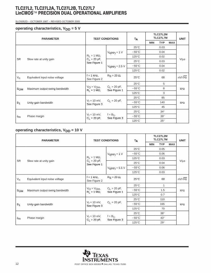
operating characteristics, V DD = 10 V
PARAMETER TEST CONDITIONS TA
TLC27L2MTLC27L7M UNITPARAMETER TEST CONDITIONS TA
MIN TYP MAXUNIT
25°C 0.05
R = 1 M ,VI(PP) = 1 V −55°C 0.06
SR Slew rate at unity gainRL = 1 MΩ,CL = 20 pF,
VI(PP) = 1 V
125°C 0.03V/ sSR Slew rate at unity gain
LCL = 20 pF,See Figure 1 25°C 0.04
V/µsSee Figure 1
VI(PP) = 5.5 V −55°C 0.06VI(PP) = 5.5 V
125°C 0.03
Vn Equivalent input noise voltagef = 1 kHz, RS = 20 Ω,
25°C 68 nV/√HzVn Equivalent input noise voltagef = 1 kHz,See Figure 2
RS = 20 Ω,25°C 68 nV/√Hz
VO = VOH, CL = 20 pF,25°C 1
BOM Maximum output-swing bandwidthVO = VOH,RL = 1 MΩ,
CL = 20 pF,See Figure 1
−55°C 1.5 kHzBOM Maximum output-swing bandwidth RL = 1 MΩ, See Figure 1125°C 0.7
kHz
VI = 10 mV, CL = 20 pF,25°C 110
B1 Unity-gain bandwidthVI = 10 mV,See Figure 3
CL = 20 pF,−55°C 165 kHzB1 Unity-gain bandwidth See Figure 3125°C 70
kHz
VI = 10 mV, f = B1,25°C 38°
φm Phase marginVI = 10 mV,CL = 20 pF,
f = B1,See Figure 3
−55°C 43°φm Phase marginCL = 20 pF, See Figure 3
125°C 29°

SLOS052D − OCTOBER 1987 − REVISED OCTOBER 2005
13POST OFFICE BOX 655303 • DALLAS, TEXAS 75265
PARAMETER MEASUREMENT INFORMATION
single-supply versus split-supply test circuits
Because the TLC27L2 and TLC27L7 are optimized for single-supply operation, circuit configurations used forthe various tests often present some inconvenience since the input signal, in many cases, must be offset fromground. This inconvenience can be avoided by testing the device with split supplies and the output load tied tothe negative rail. A comparison of single-supply versus split-supply test circuits is shown in Figure 1. The useof either circuit gives the same result.
VDD−
VDD+
−
+
CL RL
VOVIVI
VO
RLCL
VDD
−
+
(a) SINGLE SUPPLY (b) SPLIT SUPPLY
Figure 1. Unity-Gain Amplifier
VO
2 kΩ
20 Ω20 Ω
VDD−
20 Ω
2 kΩ
VO
20 Ω
1/2 VDD
−
+
VDD+−
+
VDD
(b) SPLIT SUPPLY(a) SINGLE SUPPLY
Figure 2. Noise-Test Circuit
VDD−
VDD+
−
+
10 kΩ
VO
100 Ω
CL
VIVI
1/2 VDD
CL
100 Ω
VO
10 kΩ
−
+
VDD
(a) SINGLE SUPPLY (b) SPLIT SUPPLY
Figure 3. Gain-of-100 Inverting Amplifier

SLOS052D − OCTOBER 1987 − REVISED OCTOBER 2005
14 POST OFFICE BOX 655303 • DALLAS, TEXAS 75265
PARAMETER MEASUREMENT INFORMATION
input bias current
Because of the high input impedance of the TLC27L2 and TLC27L7 operational amplifiers, attempts to measurethe input bias current can result in erroneous readings. The bias current at normal room ambient temperatureis typically less than 1 pA, a value that is easily exceeded by leakages on the test socket. Two suggestions areoffered to avoid erroneous measurements:
1. Isolate the device from other potential leakage sources.Use a grounded shield around and between thedevice inputs (see Figure 4). Leakages that would otherwise flow to the inputs are shunted away.
2. Compensate for the leakage of the test socket by actually performing an input bias current test (usinga picoammeter) with no device in the test socket. The actual input bias current can then be calculatedby subtracting the open-socket leakage readings from the readings obtained with a device in the testsocket.
One word of caution: many automatic testers as well as some bench-top operational amplifier testers use theservo-loop technique with a resistor in series with the device input to measure the input bias current (the voltagedrop across the series resistor is measured and the bias current is calculated). This method requires that adevice be inserted into the test socket to obtain a correct reading; therefore, an open-socket reading is notfeasible using this method.
8 5
1 4
V = VIC
Figure 4. Isolation Metal Around Device Inputs(JG and P packages)
low-level output voltage
To obtain low-supply-voltage operation, some compromise was necessary in the input stage. This compromiseresults in the device low-level output being dependent on both the common-mode input voltage level as wellas the differential input voltage level. When attempting to correlate low-level output readings with those quotedin the electrical specifications, these two conditions should be observed. If conditions other than these are tobe used, please refer to Figure 14 through Figure 19 in the Typical Characteristics of this data sheet.
input offset voltage temperature coefficient
Erroneous readings often result from attempts to measure temperature coefficient of input offset voltage. Thisparameter is actually a calculation using input offset voltage measurements obtained at two differenttemperatures. When one (or both) of the temperatures is below freezing, moisture can collect on both the deviceand the test socket. This moisture results in leakage and contact resistance, which can cause erroneous inputoffset voltage readings. The isolation techniques previously mentioned have no effect on the leakage since themoisture also covers the isolation metal itself, thereby rendering it useless. It is suggested that thesemeasurements be performed at temperatures above freezing to minimize error.

SLOS052D − OCTOBER 1987 − REVISED OCTOBER 2005
15POST OFFICE BOX 655303 • DALLAS, TEXAS 75265
PARAMETER MEASUREMENT INFORMATION
full-power response
Full-power response, the frequency above which the operational amplifier slew rate limits the output voltageswing, is often specified two ways: full-linear response and full-peak response. The full-linear response isgenerally measured by monitoring the distortion level of the output while increasing the frequency of a sinusoidalinput signal until the maximum frequency is found above which the output contains significant distortion. Thefull-peak response is defined as the maximum output frequency, without regard to distortion, above which fullpeak-to-peak output swing cannot be maintained.
Because there is no industry-wide accepted value for significant distortion, the full-peak response is specifiedin this data sheet and is measured using the circuit of Figure 1. The initial setup involves the use of a sinusoidalinput to determine the maximum peak-to-peak output of the device (the amplitude of the sinusoidal wave isincreased until clipping occurs). The sinusoidal wave is then replaced with a square wave of the sameamplitude. The frequency is then increased until the maximum peak-to-peak output can no longer be maintained(see Figure 5). A square wave is used to allow a more accurate determination of the point at which the maximumpeak-to-peak output is reached.
(d) f > B OM(c) f = B OM(b) BOM > f > 100 kHz(a) f = 100 kHz
Figure 5. Full-Power-Response Output Signal
test time
Inadequate test time is a frequent problem, especially when testing CMOS high-volume, short-test-timeenvironment. Internal capacitances are inherently higher in CMOS devices and require longer test times thantheir bipolar and BiFET counterparts. The problem becomes more pronounced with reduced supply levels andlower temperatures.

SLOS052D − OCTOBER 1987 − REVISED OCTOBER 2005
16 POST OFFICE BOX 655303 • DALLAS, TEXAS 75265
TYPICAL CHARACTERISTICS
Table of Graphs
FIGURE
VIO Input offset voltage Distribution 6, 7
αVIO Temperature coefficient of input offset voltage Distribution 8, 9
vs High-level output current 10, 11VOH High-level output voltage
vs High-level output currentvs Supply voltage
10, 1112VOH High-level output voltage vs Supply voltage
vs Free-air temperature1213
vs Differential input voltage 14,16VOL Low-level output voltage
vs Differential input voltagevs Free-air temperature
14,1615,17VOL Low-level output voltage vs Free-air temperature
vs Low-level output current15,1718, 19
VOL Low-level output voltage vs Free-air temperaturevs Low-level output current
15,1718, 19
vs Supply voltage 20AVD Large-signal differential voltage amplification
vs Supply voltagevs Free-air temperature
2021AVD Large-signal differential voltage amplification vs Free-air temperature
vs Frequency21
32, 33
IIB Input bias current vs Free-air temperature 22
IIO Input offset current vs Free-air temperature 22
VIC Common-mode input voltage vs Supply voltage 23
IDD Supply currentvs Supply voltage 24
IDD Supply currentvs Supply voltagevs Free-air temperature
2425
SR Slew ratevs Supply voltage 26
SR Slew ratevs Supply voltagevs Free-air temperature
2627
Normalized slew rate vs Free-air temperature 28
VO(PP) Maximum peak-to-peak output voltage vs Frequency 29
B1 Unity-gain bandwidthvs Free-air temperature 30
B1 Unity-gain bandwidthvs Free-air temperaturevs Supply voltage
3031
vs Supply voltage 34φm Phase margin
vs Supply voltagevs Free-air temperature
3435φm Phase margin vs Free-air temperature
vs Capacitive Load3536
Vn Equivalent input noise voltage vs Frequency 37
Phase shift vs Frequency 32, 33
SLOS052D − OCTOBER 1987 − REVISED OCTOBER 2005
17POST OFFICE BOX 655303 • DALLAS, TEXAS 75265
TYPICAL CHARACTERISTICS
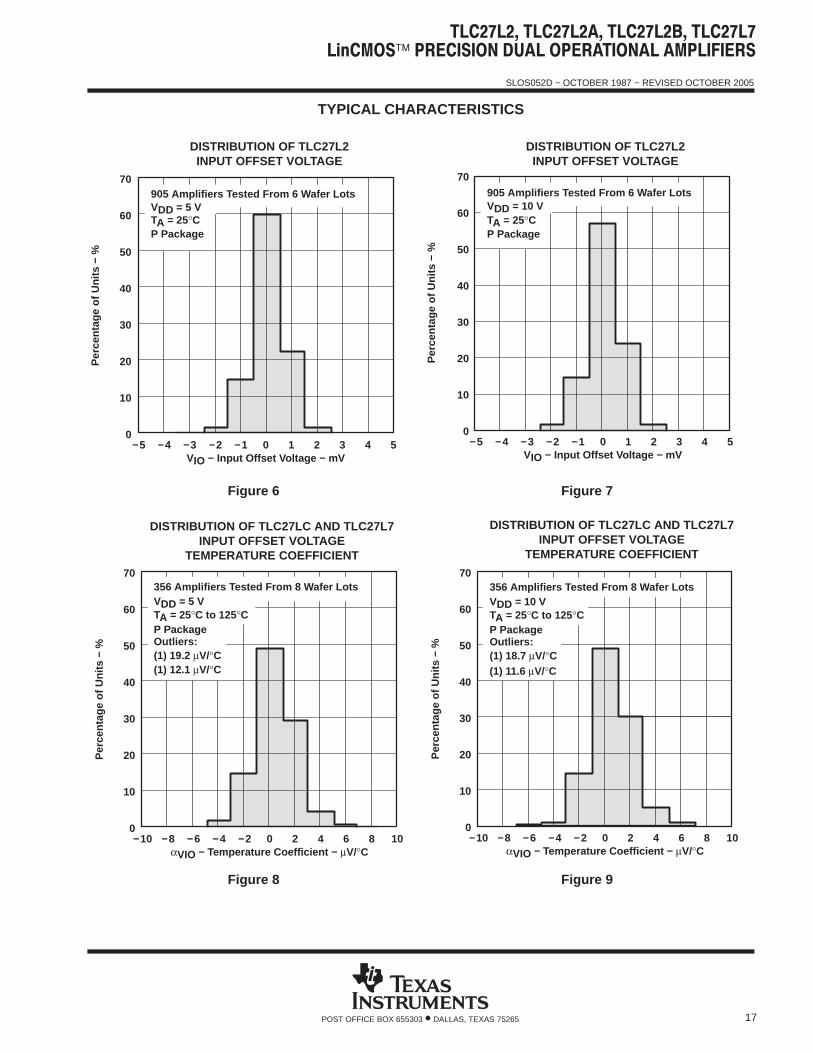
Figure 6
60
50
40
30
20
10
43210−1−2−3−4
70
5VIO − Input Offset Voltage − mV
Per
cent
age
of U
nits
− %
0−5
DISTRIBUTION OF TLC27L2INPUT OFFSET VOLTAGE
P PackageTA = 25°CVDD = 5 V905 Amplifiers Tested From 6 Wafer Lots
Figure 7
−50
Per
cent
age
of U
nits
− %
VIO − Input Offset Voltage − mV5
70
−4 −3 −2 −1 0 1 2 3 4
10
20
30
40
50
60
DISTRIBUTION OF TLC27L2INPUT OFFSET VOLTAGE
905 Amplifiers Tested From 6 Wafer LotsVDD = 10 VTA = 25°CP Package
Figure 8
−100
Per
cent
age
of U
nits
− %
αVIO − Temperature Coefficient − µV/°C10
70
−8 −6 −4 −2 0 2 4 6 8
10
20
30
40
50
60
DISTRIBUTION OF TLC27LC AND TLC27L7INPUT OFFSET VOLTAGE
TEMPERATURE COEFFICIENT
356 Amplifiers Tested From 8 Wafer LotsVDD = 5 VTA = 25°C to 125°CP PackageOutliers:(1) 19.2 µV/°C(1) 12.1 µV/°C
Figure 9
60
50
40
30
20
10
86420−2−4−6−8
70
10αVIO − Temperature Coefficient − µV/°C
Per
cent
age
of U
nits
− %
0−10
DISTRIBUTION OF TLC27LC AND TLC27L7INPUT OFFSET VOLTAGE
TEMPERATURE COEFFICIENT
(1) 11.6 µV/°C(1) 18.7 µV/°COutliers:P PackageTA = 25°C to 125°CVDD = 10 V356 Amplifiers Tested From 8 Wafer Lots
SLOS052D − OCTOBER 1987 − REVISED OCTOBER 2005
18 POST OFFICE BOX 655303 • DALLAS, TEXAS 75265
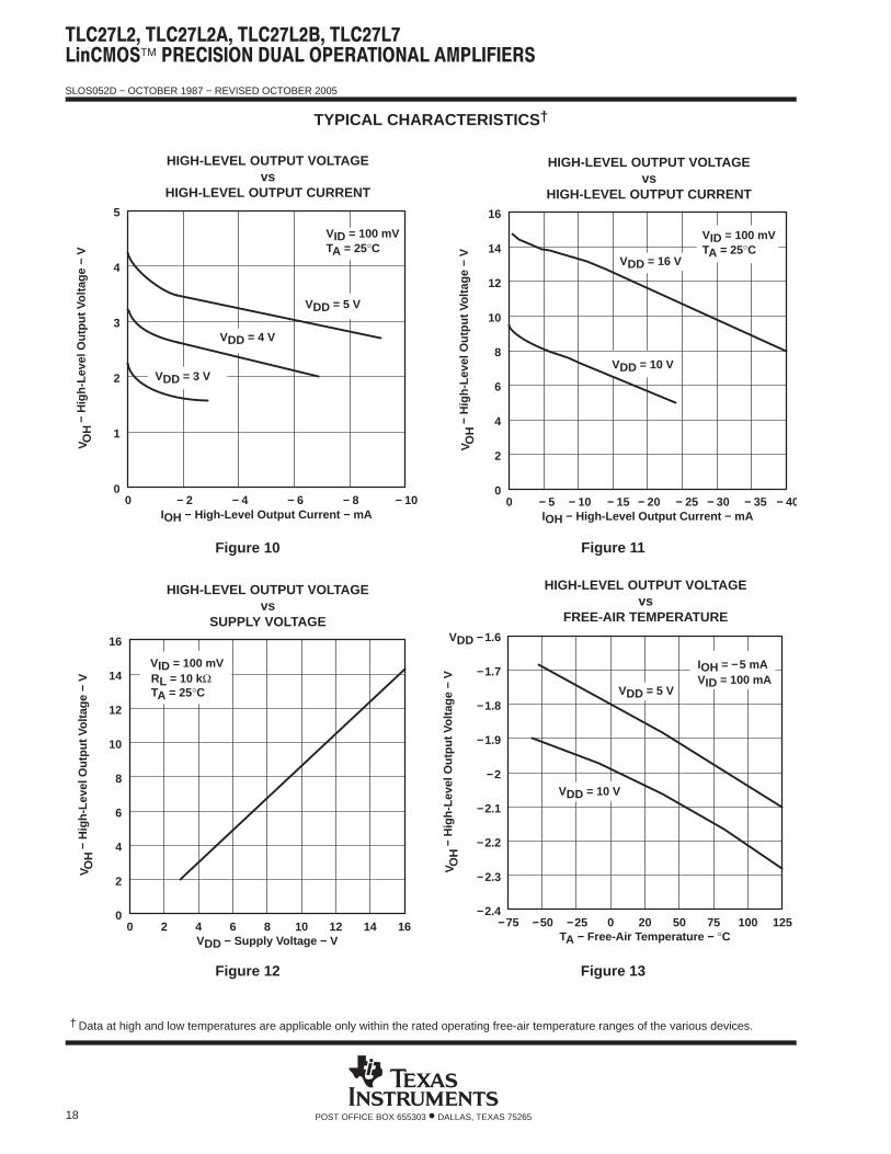
TYPICAL CHARACTERISTICS †
Figure 10
VDD = 3 V
VDD = 4 V
VDD = 5 V
4
3
2
1
− 8− 6− 4− 2
5
− 10IOH − High-Level Output Current − mA
VO
H −
Hig
h-Le
vel O
utpu
t Vol
tage
− V
00
HIGH-LEVEL OUTPUT VOLTAGEvs
HIGH-LEVEL OUTPUT CURRENT
ÁÁÁÁÁÁ
V OH
TA = 25°CVID = 100 mV
Figure 11
TA = 25°CVID = 100 mV
VDD = 10 V
14
12
10
8
6
4
2
− 30− 20− 10
16
− 40IOH − High-Level Output Current − mA
00
HIGH-LEVEL OUTPUT VOLTAGEvs
HIGH-LEVEL OUTPUT CURRENT
VO
H −
Hig
h-Le
vel O
utpu
t Vol
tage
− V
ÁÁÁÁÁÁ
V OH
− 5 − 15 − 25 − 35
ÎÎÎÎÎÎÎÎÎÎ
VDD = 16 V
Figure 12
ÎÎÎÎÎÎÎÎÎÎ
TA = 25°CÎÎÎÎÎÎRL = 10 kΩÎÎÎÎÎVID = 100 mV
0
16
2
4
6
8
10
12
14
1412108642 16VDD − Supply Voltage − V
0
HIGH-LEVEL OUTPUT VOLTAGEvs
SUPPLY VOLTAGE
VO
H −
Hig
h-Le
vel O
utpu
t Vol
tage
− V
ÁÁÁÁÁÁ
V OH
Figure 13
VDD = 10 V
VDD = 5 V
−75−2.4
TA − Free-Air Temperature − °C125
VDD −1.6
−50 −25 0 20 50 75 100
−2.3
−2.2
−2.1
−2
−1.9
−1.8
−1.7
HIGH-LEVEL OUTPUT VOLTAGEvs
FREE-AIR TEMPERATURE
VO
H −
Hig
h-Le
vel O
utpu
t Vol
tage
− V
ÁÁÁÁÁÁ
V OH
ÁÁÁÁÁÁÁÁÁÁVID = 100 mA
IOH = −5 mA
† Data at high and low temperatures are applicable only within the rated operating free-air temperature ranges of the various devices.

SLOS052D − OCTOBER 1987 − REVISED OCTOBER 2005
19POST OFFICE BOX 655303 • DALLAS, TEXAS 75265
TYPICAL CHARACTERISTICS †
Figure 14
VID = −1 V
VID = −100 mV
VDD = 5 VIOL = 5 mATA = 25°C
600
500
400
321
700
4VIC − Common-Mode Input Voltage − V
VO
L −
Low
-Lev
el O
utpu
t Vol
tage
− m
V
3000
LOW-LEVEL OUTPUT VOLTAGEvs
DIFFERENTIAL INPUT VOLTAGE
0.5 1.5 2.5 3.3
ÁÁÁÁ
VO
L
Figure 15
VID = −100 mV
VID = − 2.5 V
VID = −1 V
TA = 25°CIOL = 5 mAVDD = 10 V
108642
500
450
400
350
300
VIC − Common-Mode Input Voltage − V0
250
LOW-LEVEL OUTPUT VOLTAGEvs
FREE-AIR TEMPERATURE
VO
L −
Low
-Lev
el O
utpu
t Vol
tage
− m
V
ÁÁÁÁ
VO
L1 3 5 7 9
Figure 16
TA = 25°CVIC = |VID/2|IOL = 5 mA
0
100
200
300
400
500
600
700
800
−8−6−4−2 −10VID − Differential Input Voltage − V
0
LOW-LEVEL OUTPUT VOLTAGEvs
DIFFERENTIAL INPUT VOLTAGE
−1 −3 −5 −7 −9
VO
L −
Low
-Lev
el O
utpu
t Vol
tage
− m
V
ÁÁÁÁ
VO
L
ÎÎÎÎÎÎÎÎÎÎ
VDD = 10 V
ÎÎÎÎÎÎÎÎ
VDD = 5 V
Figure 17
VDD = 5 V
800
700
600
500
400
300
200
100
1007550250−25−50
900
125TA − Free-Air Temperature − °C
0−75
LOW-LEVEL OUTPUT VOLTAGEvs
FREE-AIR TEMPERATURE
VO
L −
Low
-Lev
el O
utpu
t Vol
tage
− m
V
ÁÁÁÁÁÁ
VO
L
ÁÁÁÁÁÁÁÁÁÁÁÁÁÁÁÁ
IOL = 5 mAVID = −1 VVIC = 0.5 V
ÎÎÎÎÎÎÎÎÎÎ
VDD = 10 V
† Data at high and low temperatures are applicable only within the rated operating free-air temperature ranges of the various devices.
SLOS052D − OCTOBER 1987 − REVISED OCTOBER 2005
20 POST OFFICE BOX 655303 • DALLAS, TEXAS 75265
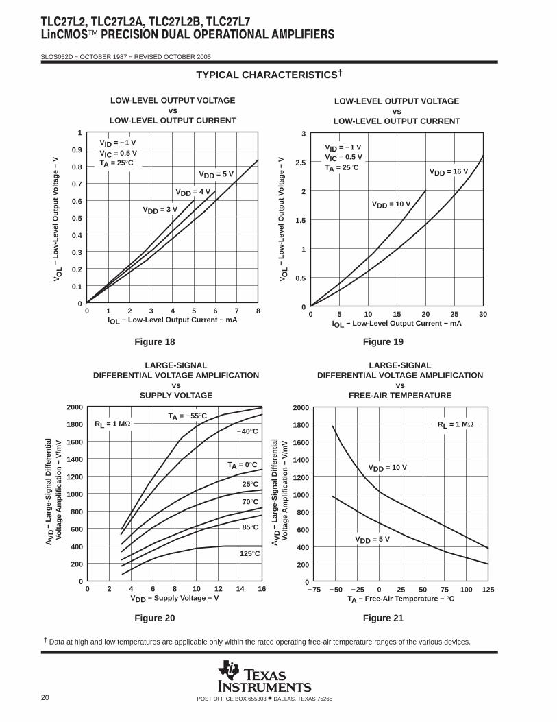
TYPICAL CHARACTERISTICS †
Figure 18
LOW-LEVEL OUTPUT VOLTAGEvs
LOW-LEVEL OUTPUT CURRENT
VDD = 4 V
VDD = 3 V
ÎÎÎÎÎTA = 25°CÎÎÎÎÎÎÎÎÎÎ
VIC = 0.5 V
ÎÎÎÎÎÎÎÎÎÎ
VID = −1 V0.9
0.8
0.7
0.6
0.5
0.4
0.3
0.2
0.1
76543210
8
1
IOL − Low-Level Output Current − mA0
VO
L −
Low
-Lev
el O
utpu
t Vol
tage
− V
ÁÁÁÁÁÁ
VO
L
ÎÎÎÎÎVDD = 5 V
Figure 19
LOW-LEVEL OUTPUT VOLTAGEvs
LOW-LEVEL OUTPUT CURRENT
VDD = 16 V
VDD = 10 V
ÎÎÎÎÎÎVID = −1 VÎÎÎÎÎÎÎÎÎÎÎÎVIC = 0.5 VÎÎÎÎÎÎÎÎÎÎTA = 25°C
2.5
2
1.5
1
0.5
2520151050
30
3
IOL − Low-Level Output Current − mA0
VO
L −
Low
-Lev
el O
utpu
t Vol
tage
− V
ÁÁÁÁÁÁ
VO
L
Figure 20
0VDD − Supply Voltage − V
2000
160
2 4 6 8 10 12 14
200
400
600
800
1000
1200
1400
1600
1800 RL = 1 MΩTA = −55°C
−40°C
TA = 0°C
ÎÎÎÎ
70°C
ÎÎ85°C
125°C
LARGE-SIGNALDIFFERENTIAL VOLTAGE AMPLIFICATION
vsSUPPLY VOLTAGE
ÎÎ25°C
AV
D −
Lar
ge-S
igna
l Diff
eren
tial
ÁÁÁ
AV
DV
olta
ge A
mpl
ifica
tion
− V
/mV
Figure 21
LARGE-SIGNALDIFFERENTIAL VOLTAGE AMPLIFICATION
vsFREE-AIR TEMPERATURE
1007550250−25−500
125TA − Free-Air Temperature − °C
−75
RL = 1 MΩ
VDD = 5 V
VDD = 10 V
1800
1600
1400
1200
1000
800
600
400
200
2000
AV
D −
Lar
ge-S
igna
l Diff
eren
tial
ÁÁÁÁÁÁ
AV
DV
olta
ge A
mpl
ifica
tion
− V
/mV
† Data at high and low temperatures are applicable only within the rated operating free-air temperature ranges of the various devices.

SLOS052D − OCTOBER 1987 − REVISED OCTOBER 2005
21POST OFFICE BOX 655303 • DALLAS, TEXAS 75265
TYPICAL CHARACTERISTICS †
Figure 22
0.1125
10000
45 65 85 105
1
10
100
1000
25
IIB a
nd II
O −
Inpu
t Bia
s an
d O
ffset
Cur
rent
s −
pA
TA − Free-Air Temperature − °C
INPUT BIAS CURRENT AND INPUT OFFSET CURRENTvs
FREE-AIR TEMPERATURE
IBII I
O
ÁÁÁÁÁÁÁÁÁÁÁÁÁÁÁÁ
VDD = 10 VVIC = 5 VSee Note A
ÎÎIIB
ÎÎIIO
NOTE A: The typical values of input bias current and input offsetcurrent below 5 pA were determined mathematically.
Figure 23
COMMON-MODEINPUT VOLTAGE POSITIVE LIMIT
vsSUPPLY VOLTAGE
0
VI −
Com
mon
-Mod
e In
put V
olta
ge −
V
VDD − Supply Voltage − V
16
160
2 4 6 8 10 12 14
2
4
6
8
10
12
14TA = 25°C
ÁÁÁÁ
VIC
Figure 24
No LoadVO = VDD/2
0°C
−40°C
80
70
60
50
40
30
20
10
14121086420
16
90
VDD − Supply Voltage − V
IDD
− S
uppl
y C
urre
nt −
mA
0
125°C
70°C
25°C
TA = −55°C
SUPPLY CURRENTvs
SUPPLY VOLTAGE
ÁÁÁÁ
DD
IA
µ
Figure 25
50
40
30
20
10
1007550250−25−500
125
60
TA − Free-Air Temperature − °C−75
VDD = 5 V
VDD = 10 V
No LoadVO = VDD/2
SUPPLY CURRENTvs
FREE-AIR TEMPERATURE
IDD
− S
uppl
y C
urre
nt −
mA
ÁÁÁÁ
DD
IA
µ
† Data at high and low temperatures are applicable only within the rated operating free-air temperature ranges of the various devices.

SLOS052D − OCTOBER 1987 − REVISED OCTOBER 2005
22 POST OFFICE BOX 655303 • DALLAS, TEXAS 75265
TYPICAL CHARACTERISTICS †
Figure 26
See Figure 1TA = 25°C
0
SR
− S
lew
Rat
e −
V/s
VDD − Supply Voltage − V
0.07
160.00
2 4 6 8 10 12 14
0.01
0.02
0.03
0.04
0.05
0.06
SLEW RATEvs
SUPPLY VOLTAGE
CL = 20 pFRL =1 MΩVI(PP) = 1 VAV = 1
sµ
Figure 27
VI(PP) = 5.5 VVDD = 10 V
−75TA − Free-Air Temperature − °C
0.07
1250.00
−50 −25 0 25 50 75 100
0.01
0.02
0.03
0.04
0.05
0.06
SLEW RATEvs
FREE-AIR TEMPERATURE
RL =1 MΩCL = 20 pFAV = 1See Figure 1
VI(PP) = 1 VVDD = 10 V
VI(PP) = 1 VVDD = 5 V
VI(PP) = 2.5 VVDD = 5 V
SR
− S
lew
Rat
e −
V/s
sµ
Figure 28
0.5
0.6
0.7
0.8
0.9
1
1.1
1.2
1.3
1.4
1007550250−25−50 125TA − Free-Air Temperature − °C
Nor
mal
ized
Sle
w R
ate
−75
NORMALIZED SLEW RATEvs
FREE-AIR TEMPERATURE
CL = 20 pFRL =1 MΩVIPP = 1 VAV = 1
ÎÎÎÎÎÎÎÎÎÎ
VDD = 10 V
ÎÎÎÎVDD = 5 V
Figure 29
101
9
8
7
6
5
4
3
2
1
0100
10
f − Frequency − kHz0.1
MAXIMUM-PEAK-TO-PEAK OUTPUT VOLTAGEvs
FREQUENCY
ÁÁÁÁÁÁ
RL = 1 MΩSee Figure 1
ÎÎÎÎÎÎÎÎ
VDD = 5 V
TA = −55°CTA = 25°CTA = 125°CÎÎÎÎ
ÎÎÎÎVDD = 10 V
− M
axim
um P
eak-
to-P
eak
Out
put V
olta
ge −
VV O
(PP
)
† Data at high and low temperatures are applicable only within the rated operating free-air temperature ranges of the various devices.
SLOS052D − OCTOBER 1987 − REVISED OCTOBER 2005
23POST OFFICE BOX 655303 • DALLAS, TEXAS 75265
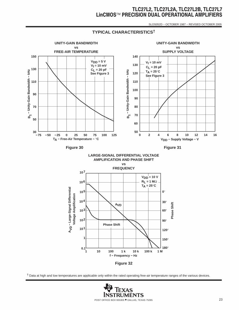
TYPICAL CHARACTERISTICS †
Figure 30
VDD = 5 VVI = 10 mVCL = 20 pFSee Figure 3
−75
B1
− U
nity
-Gai
n B
andw
idth
− k
Hz
TA − Free-Air Temperature − °C
150
12530
−50 −25 0 25 50 75 100
50
70
90
110
130
UNITY-GAIN BANDWIDTHvs
FREE-AIR TEMPERATURE
B1
Figure 31
0VDD − Supply Voltage − V
140
1650
2 4 6 8 10 12 14
60
70
80
90
100
110
120
130
See Figure 3TA = 25°CCL = 20 pF
VI = 10 mV
UNITY-GAIN BANDWIDTHvs
SUPPLY VOLTAGE
B1
− U
nity
-Gai
n B
andw
idth
− k
Hz
B1
1f − Frequency − Hz
1 M10 100 1 k 10 k 100 k
Pha
se S
hiftAVD
ÎÎÎÎÎPhase Shift
180°
0°
30°
60°
90°
120°
150°
107
106
0.1
1
105
104
103
102
101
VDD = 10 VRL = 1 MΩTA = 25°C
LARGE-SIGNAL DIFFERENTIAL VOLTAGEAMPLIFICATION AND PHASE SHIFT
vsFREQUENCY
AV
D −
Lar
ge-S
igna
l Diff
eren
tial
ÁÁÁÁÁÁ
AV
DV
olta
ge A
mpl
ifica
tion
Figure 32
† Data at high and low temperatures are applicable only within the rated operating free-air temperature ranges of the various devices.

SLOS052D − OCTOBER 1987 − REVISED OCTOBER 2005
24 POST OFFICE BOX 655303 • DALLAS, TEXAS 75265
TYPICAL CHARACTERISTICS †
ÎÎÎÎÎÎÎÎÎÎPhase Shift
AVD
VDD = 10 VRL = 1 MΩTA = 25°C
Pha
se S
hift
180°
0°
30°
60°
90°
120°
150°
100 k10 k1 k10010 1 Mf − Frequency − Hz
1
10 7
LARGE-SIGNAL DIFFERENTIAL VOLTAGEAMPLIFICATION AND PHASE SHIFT
vsFREQUENCY
10 6
0.1
1
10 5
10 4
10 3
10 2
10 1AV
D −
Lar
ge-S
igna
l Diff
eren
tial
ÁÁÁÁÁÁ
AV
DV
olta
ge A
mpl
ifica
tion
Figure 33
Figure 34
0
m −
Pha
se M
argi
n
VDD − Supply Voltage − V
42°
1630°
2 4 6 8 10 12 14
32°
34°
36°
38°
40°
See Figure 3
VI = 10 mV
TA = 25°CCL = 20 pF
ÁÁ
mφ
PHASE MARGINvs
SUPPLY VOLTAGE
Figure 35
See Figure 3
VI = 10 mVCL = 20 pF
VDD = 5 mV
−75
TA − Free-Air Temperature − °C
40°
12520°
− 50 −25 0 25 50 75 100
24°
28°
32°
36°
m −
Pha
se M
argi
n
ÁÁÁÁ
mφ
PHASE MARGINvs
FREE-AIR TEMPERATURE
† Data at high and low temperatures are applicable only within the rated operating free-air temperature ranges of the various devices.
SLOS052D − OCTOBER 1987 − REVISED OCTOBER 2005
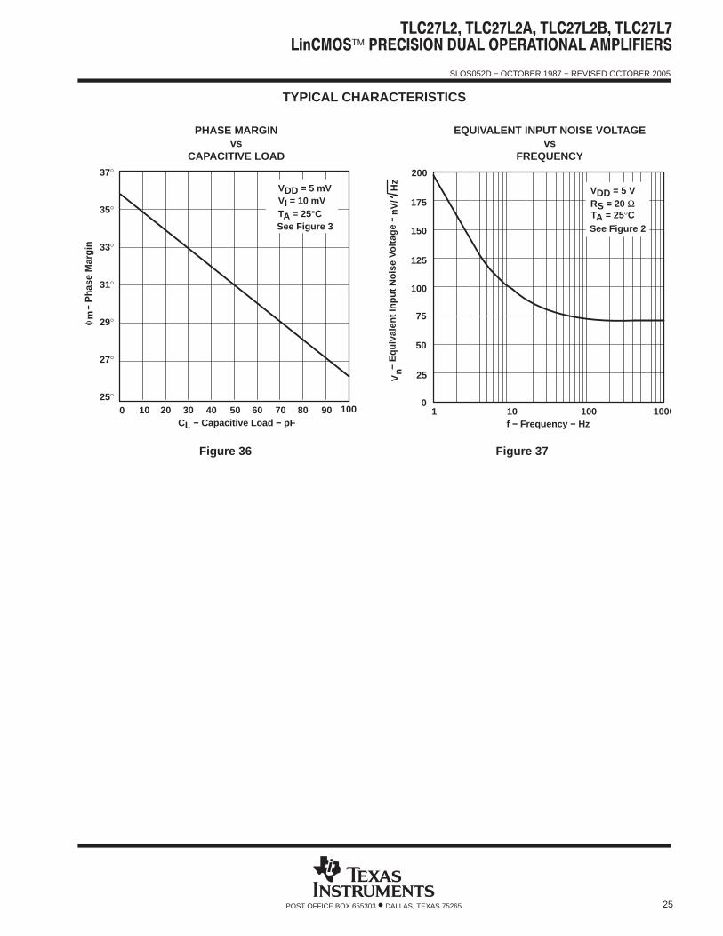
25POST OFFICE BOX 655303 • DALLAS, TEXAS 75265
TYPICAL CHARACTERISTICS
Figure 36
VDD = 5 mV
TA = 25°CSee Figure 3
VI = 10 mV
0CL − Capacitive Load − pF
37°
10025°
20 40 60 80
27°
29°
31°
33°
35°
PHASE MARGINvs
CAPACITIVE LOAD
m −
Pha
se M
argi
n
ÁÁÁÁ
mφ
10 30 50 70 90
Figure 37
See Figure 2
RS = 20 ΩVDD = 5 V
1
VN
− E
quiv
alen
t Inp
ut N
oise
Vol
tage
− n
V/H
z
f − Frequency − Hz100010 100
EQUIVALENT INPUT NOISE VOLTAGEvs
FREQUENCY
TA = 25°C
200
175
150
125
100
75
50
25
0V
n
ÁÁÁÁÁÁÁÁ
nV/
Hz
SLOS052D − OCTOBER 1987 − REVISED OCTOBER 2005
26 POST OFFICE BOX 655303 • DALLAS, TEXAS 75265
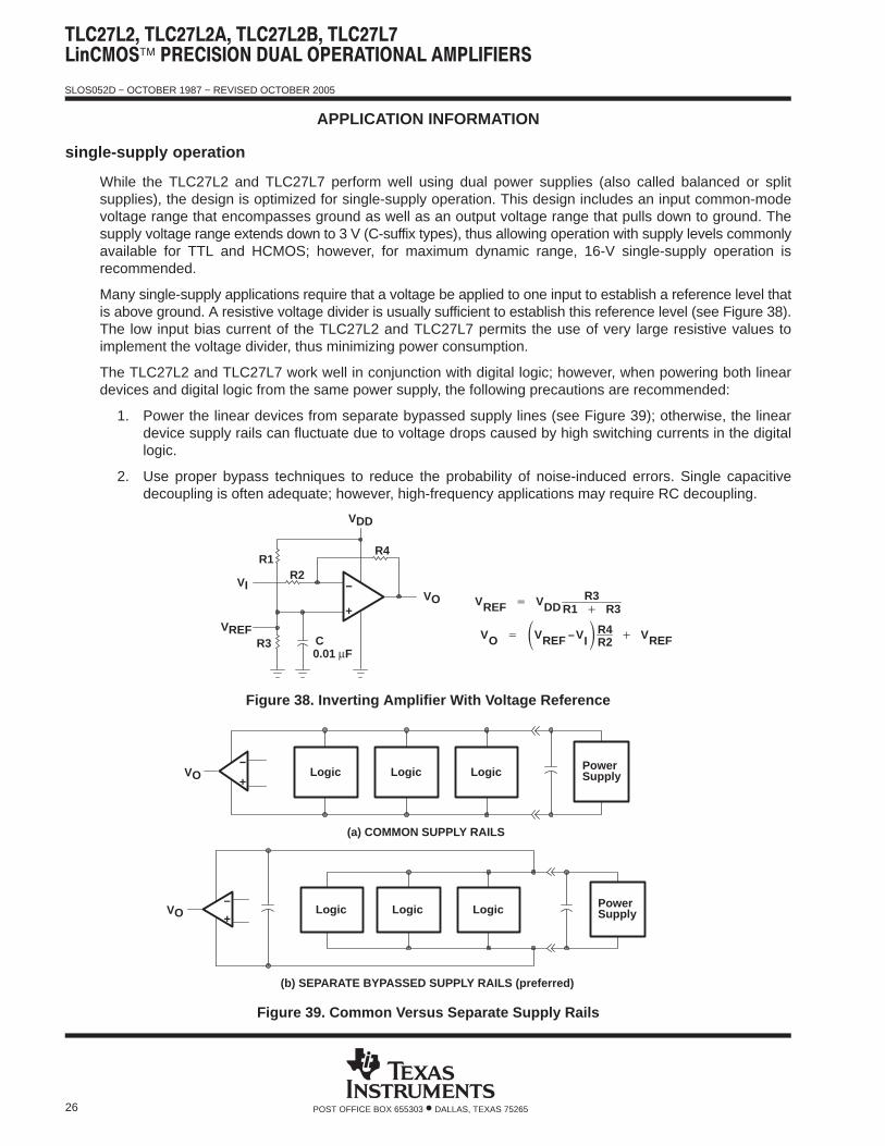
APPLICATION INFORMATION
single-supply operation
While the TLC27L2 and TLC27L7 perform well using dual power supplies (also called balanced or splitsupplies), the design is optimized for single-supply operation. This design includes an input common-modevoltage range that encompasses ground as well as an output voltage range that pulls down to ground. Thesupply voltage range extends down to 3 V (C-suffix types), thus allowing operation with supply levels commonlyavailable for TTL and HCMOS; however, for maximum dynamic range, 16-V single-supply operation isrecommended.
Many single-supply applications require that a voltage be applied to one input to establish a reference level thatis above ground. A resistive voltage divider is usually sufficient to establish this reference level (see Figure 38).The low input bias current of the TLC27L2 and TLC27L7 permits the use of very large resistive values toimplement the voltage divider, thus minimizing power consumption.
The TLC27L2 and TLC27L7 work well in conjunction with digital logic; however, when powering both lineardevices and digital logic from the same power supply, the following precautions are recommended:
1. Power the linear devices from separate bypassed supply lines (see Figure 39); otherwise, the lineardevice supply rails can fluctuate due to voltage drops caused by high switching currents in the digitallogic.
2. Use proper bypass techniques to reduce the probability of noise-induced errors. Single capacitivedecoupling is often adequate; however, high-frequency applications may require RC decoupling.
−
+
0.01 µFCR3
VREF
VI
R1R2
VDD
VO
R4
VREF VDDR3
R1 R3
VO VREF –VIR4
R2 VREF
Figure 38. Inverting Amplifier With Voltage Reference
(b) SEPARATE BYPASSED SUPPLY RAILS (preferred)
(a) COMMON SUPPLY RAILS
−
+
−
+
Logic Logic Logic
SupplyPowerLogicLogicLogic
SupplyPower
VO
VO
Figure 39. Common Versus Separate Supply Rails

SLOS052D − OCTOBER 1987 − REVISED OCTOBER 2005
27POST OFFICE BOX 655303 • DALLAS, TEXAS 75265
APPLICATION INFORMATION
input characteristics
The TLC27L2 and TLC27L7 are specified with a minimum and a maximum input voltage that, if exceeded ateither input, could cause the device to malfunction. Exceeding this specified range is a common problem,especially in single-supply operation. Note that the lower range limit includes the negative rail, while the upperrange limit is specified at VDD −1 V at TA = 25°C and at VDD −1.5 V at all other temperatures.
The use of the polysilicon-gate process and the careful input circuit design gives the TLC27L2 and TLC27L7very good input offset voltage drift characteristics relative to conventional metal-gate processes. Offset voltagedrift in CMOS devices is highly influenced by threshold voltage shifts caused by polarization of the phosphorusdopant implanted in the oxide. Placing the phosphorus dopant in a conductor (such as a polysilicon gate)alleviates the polarization problem, thus reducing threshold voltage shifts by more than an order of magnitude.The offset voltage drift with time has been calculated to be typically 0.1 µV/month, including the first month ofoperation.
Because of the extremely high input impedance and resulting low bias current requirements, the TLC27L2 andTLC27L7 are well suited for low-level signal processing; however, leakage currents on printed circuit boardsand sockets can easily exceed bias current requirements and cause a degradation in device performance. Itis good practice to include guard rings around inputs (similar to those of Figure 4 in the Parameter MeasurementInformation section). These guards should be driven from a low-impedance source at the same voltage levelas the common-mode input (see Figure 40).
Unused amplifiers should be connected as grounded unity-gain followers to avoid possible oscillation.
noise performance
The noise specifications in operational amplifier circuits are greatly dependent on the current in the first-stagedifferential amplifier. The low input bias current requirements of the TLC27L2 and TLC27L7 result in a low noisecurrent, which is insignificant in most applications. This feature makes the devices especially favorable overbipolar devices when using values of circuit impedance greater than 50 kΩ, since bipolar devices exhibit greaternoise currents.
VI
−
+
−
+
VI
(b) INVERTING AMPLIFIER
−
+
(c) UNITY-GAIN AMPLIFIER(a) NONINVERTING AMPLIFIER
VI
VO VO VO
Figure 40. Guard-Ring Schemes
output characteristics
The output stage of the TLC27L2 and TLC27L7 is designed to sink and source relatively high amounts of current(see typical characteristics). If the output is subjected to a short-circuit condition, this high current capability cancause device damage under certain conditions. Output current capability increases with supply voltage.
All operating characteristics of the TLC27L2 and TLC27L7 were measured using a 20-pF load. The devicesdrive higher capacitive loads; however, as output load capacitance increases, the resulting response poleoccurs at lower frequencies, thereby causing ringing, peaking, or even oscillation (see Figure 41). In manycases, adding a small amount of resistance in series with the load capacitance alleviates the problem.

SLOS052D − OCTOBER 1987 − REVISED OCTOBER 2005
28 POST OFFICE BOX 655303 • DALLAS, TEXAS 75265
APPLICATION INFORMATION
output characteristics (continued)
(b) CL = 260 pF, RL = NO LOAD(a) CL = 20 pF, RL = NO LOAD
VI
−2.5 V
CL
VO
2.5 V
−
+
TA = 25°Cf = 1 kHzVI(PP) = 1 V
(d) TEST CIRCUIT(c) CL = 310 pF, RL = NO LOAD
Figure 41. Effect of Capacitive Loads and Test Circuit
Although the TLC27L2 and TLC27L7 possess excellent high-level output voltage and current capability,methods for boosting this capability are available, if needed. The simplest method involves the use of a pullupresistor (RP) connected from the output to the positive supply rail (see Figure 42). There are two disadvantagesto the use of this circuit. First, the NMOS pulldown transistor N4 (see equivalent schematic) must sink acomparatively large amount of current. In this circuit, N4 behaves like a linear resistor with an on-resistancebetween approximately 60 Ω and 180 Ω, depending on how hard the operational amplifier input is driven. Withvery low values of RP, a voltage offset from 0 V at the output occurs. Second, pullup resistor RP acts as adrain load to N4 and the gain of the operational amplifier is reduced at output voltage levels where N5 is notsupplying the output current.

SLOS052D − OCTOBER 1987 − REVISED OCTOBER 2005
29POST OFFICE BOX 655303 • DALLAS, TEXAS 75265
APPLICATION INFORMATION
output characteristics (continued)
Figure 42. Resistive Pullup to Increase V OH
IL
IF
IP
RLR1R2
VO
RP
VDD
VI
−
+
RP VDD–VO
IF IL IP
ÁÁÁÁÁÁÁÁÁÁÁÁÁÁÁÁÁÁÁÁÁÁÁÁÁÁÁ
IP = Pullup current required by the operational amplifier (typically 500 µA)
Figure 43. Compensation for Input Capacitance
C
−
+
VO
feedback
Operational amplifier circuits nearly always employ feedback, and since feedback is the first prerequisite foroscillation, some caution is appropriate. Most oscillation problems result from driving capacitive loads(discussed previously) and ignoring stray input capacitance. A small-value capacitor connected in parallel withthe feedback resistor is an effective remedy (see Figure 43). The value of this capacitor is optimized empirically.
electrostatic discharge protection
The TLC27L2 and TLC27L7 incorporate an internal electrostatic discharge (ESD) protection circuit thatprevents functional failures at voltages up to 2000 V as tested under MIL-STD-883C, Method 3015.2. Careshould be exercised, however, when handling these devices, as exposure to ESD may result in the degradationof the device parametric performance. The protection circuit also causes the input bias currents to betemperature dependent and have the characteristics of a reverse-biased diode.
latch-up
Because CMOS devices are susceptible to latch-up due to their inherent parasitic thyristors, the TLC27L2 andTLC27L7 inputs and outputs were designed to withstand −100-mA surge currents without sustaining latch-up;however, techniques should be used to reduce the chance of latch-up whenever possible. Internal protectiondiodes should not, by design, be forward biased. Applied input and output voltage should not exceed the supplyvoltage by more than 300 mV. Care should be exercised when using capacitive coupling on pulse generators.Supply transients should be shunted by the use of decoupling capacitors (0.1 µF typical) located across thesupply rails as close to the device as possible.
The current path established if latch-up occurs is usually between the positive supply rail and ground and canbe triggered by surges on the supply lines and/or voltages on either the output or inputs that exceed the supplyvoltage. Once latch-up occurs, the current flow is limited only by the impedance of the power supply and theforward resistance of the parasitic thyristor and usually results in the destruction of the device. The chance oflatch-up occurring increases with increasing temperature and supply voltages.

SLOS052D − OCTOBER 1987 − REVISED OCTOBER 2005
30 POST OFFICE BOX 655303 • DALLAS, TEXAS 75265
APPLICATION INFORMATION
−
+
−
+
500 kΩ
500 kΩ
5 V
500 kΩ
0.1 µF
500 kΩ
VO2
VO1
1/2TLC27L2
TLC27L21/2
Figure 44. Multivibrator
Reset
Set
TLC27L21/2−
+
100 kΩ
VDD
33 kΩ
100 kΩ
100 kΩ
NOTE: VDD = 5 V to 16 V
Figure 45. Set/Reset Flip-Flop
SLOS052D − OCTOBER 1987 − REVISED OCTOBER 2005
31POST OFFICE BOX 655303 • DALLAS, TEXAS 75265
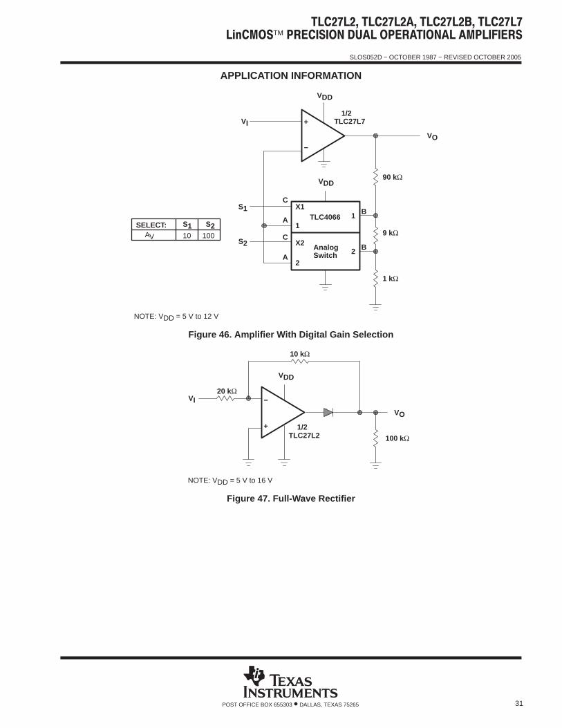
APPLICATION INFORMATION
−
+
VDD
VO
90 kΩ
9 kΩ
X1
11 B
TLC4066
VDD
VI
S1
S2
C
A
C
A2
X22 B
1 kΩ
AnalogSwitch
1/2TLC27L7
SELECT: S1 S2AV 10 100
NOTE: VDD = 5 V to 12 V
Figure 46. Amplifier With Digital Gain Selection−
+
10 kΩ
VO
100 kΩ
VDD
20 kΩVI
1/2TLC27L2
NOTE: VDD = 5 V to 16 V
Figure 47. Full-Wave Rectifier
SLOS052D − OCTOBER 1987 − REVISED OCTOBER 2005
32 POST OFFICE BOX 655303 • DALLAS, TEXAS 75265
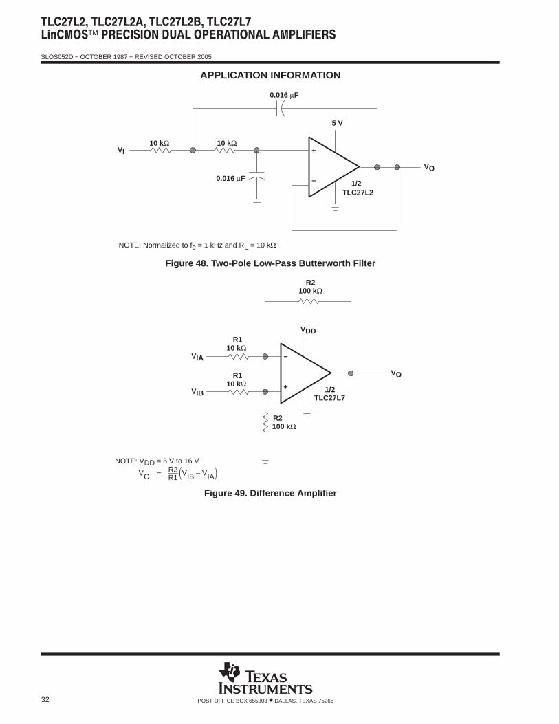
APPLICATION INFORMATION
TLC27L21/2
VI
0.016 µF
VO
10 kΩ
5 V
−
+10 kΩ
0.016 µF
NOTE: Normalized to fc = 1 kHz and RL = 10 kΩ
Figure 48. Two-Pole Low-Pass Butterworth Filter
−
+
VO
1/2TLC27L7
R2100 kΩ
R110 kΩ
100 kΩR2
VIB
VDD
VIA
R110 kΩ
NOTE: VDD = 5 V to 16 V
VO R2R1VIB – VIA
Figure 49. Difference Amplifier

PACKAGE OPTION ADDENDUM
www.ti.com 17-Mar-2017
Addendum-Page 1
PACKAGING INFORMATION
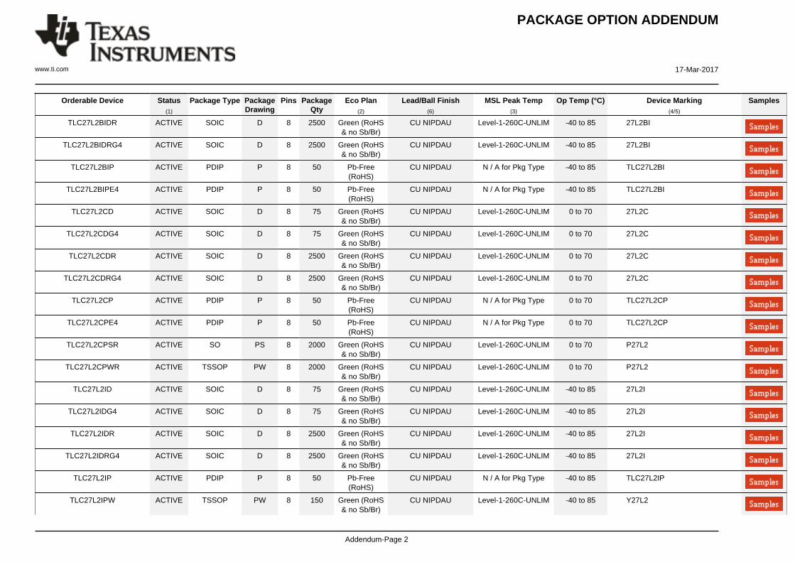
Orderable Device Status(1)
Package Type PackageDrawing
Pins PackageQty
Eco Plan(2)
Lead/Ball Finish(6)
MSL Peak Temp(3)
Op Temp (°C) Device Marking(4/5)
Samples
TLC27L2ACD ACTIVE SOIC D 8 75 Green (RoHS& no Sb/Br)
CU NIPDAU Level-1-260C-UNLIM 0 to 70 27L2AC
TLC27L2ACDG4 ACTIVE SOIC D 8 75 Green (RoHS& no Sb/Br)
CU NIPDAU Level-1-260C-UNLIM 0 to 70 27L2AC
TLC27L2ACDR ACTIVE SOIC D 8 2500 Green (RoHS& no Sb/Br)
CU NIPDAU Level-1-260C-UNLIM 0 to 70 27L2AC
TLC27L2ACDRG4 ACTIVE SOIC D 8 2500 Green (RoHS& no Sb/Br)
CU NIPDAU Level-1-260C-UNLIM 0 to 70 27L2AC
TLC27L2ACP ACTIVE PDIP P 8 50 Pb-Free(RoHS)
CU NIPDAU N / A for Pkg Type 0 to 70 TLC27L2AC
TLC27L2AID ACTIVE SOIC D 8 75 Green (RoHS& no Sb/Br)
CU NIPDAU Level-1-260C-UNLIM -40 to 85 27L2AI
TLC27L2AIDG4 ACTIVE SOIC D 8 75 Green (RoHS& no Sb/Br)
CU NIPDAU Level-1-260C-UNLIM -40 to 85 27L2AI
TLC27L2AIDR ACTIVE SOIC D 8 2500 Green (RoHS& no Sb/Br)
CU NIPDAU Level-1-260C-UNLIM -40 to 85 27L2AI
TLC27L2AIDRG4 ACTIVE SOIC D 8 2500 Green (RoHS& no Sb/Br)
CU NIPDAU Level-1-260C-UNLIM -40 to 85 27L2AI
TLC27L2AIP ACTIVE PDIP P 8 50 Pb-Free(RoHS)
CU NIPDAU N / A for Pkg Type -40 to 85 TLC27L2AI
TLC27L2BCD ACTIVE SOIC D 8 75 Green (RoHS& no Sb/Br)
CU NIPDAU Level-1-260C-UNLIM 0 to 70 27L2BC
TLC27L2BCDG4 ACTIVE SOIC D 8 75 Green (RoHS& no Sb/Br)
CU NIPDAU Level-1-260C-UNLIM 0 to 70 27L2BC
TLC27L2BCDR ACTIVE SOIC D 8 2500 Green (RoHS& no Sb/Br)
CU NIPDAU Level-1-260C-UNLIM 0 to 70 27L2BC
TLC27L2BCDRG4 ACTIVE SOIC D 8 2500 Green (RoHS& no Sb/Br)
CU NIPDAU Level-1-260C-UNLIM 0 to 70 27L2BC
TLC27L2BCP ACTIVE PDIP P 8 50 Pb-Free(RoHS)
CU NIPDAU N / A for Pkg Type 0 to 70 TLC27L2BC
TLC27L2BID ACTIVE SOIC D 8 75 Green (RoHS& no Sb/Br)
CU NIPDAU Level-1-260C-UNLIM -40 to 85 27L2BI
TLC27L2BIDG4 ACTIVE SOIC D 8 75 Green (RoHS& no Sb/Br)
CU NIPDAU Level-1-260C-UNLIM -40 to 85 27L2BI
PACKAGE OPTION ADDENDUM
www.ti.com 17-Mar-2017
Addendum-Page 2
Orderable Device Status(1)
Package Type PackageDrawing
Pins PackageQty
Eco Plan(2)
Lead/Ball Finish(6)
MSL Peak Temp(3)
Op Temp (°C) Device Marking(4/5)
Samples
TLC27L2BIDR ACTIVE SOIC D 8 2500 Green (RoHS& no Sb/Br)
CU NIPDAU Level-1-260C-UNLIM -40 to 85 27L2BI
TLC27L2BIDRG4 ACTIVE SOIC D 8 2500 Green (RoHS& no Sb/Br)
CU NIPDAU Level-1-260C-UNLIM -40 to 85 27L2BI
TLC27L2BIP ACTIVE PDIP P 8 50 Pb-Free(RoHS)
CU NIPDAU N / A for Pkg Type -40 to 85 TLC27L2BI
TLC27L2BIPE4 ACTIVE PDIP P 8 50 Pb-Free(RoHS)
CU NIPDAU N / A for Pkg Type -40 to 85 TLC27L2BI
TLC27L2CD ACTIVE SOIC D 8 75 Green (RoHS& no Sb/Br)
CU NIPDAU Level-1-260C-UNLIM 0 to 70 27L2C
TLC27L2CDG4 ACTIVE SOIC D 8 75 Green (RoHS& no Sb/Br)
CU NIPDAU Level-1-260C-UNLIM 0 to 70 27L2C
TLC27L2CDR ACTIVE SOIC D 8 2500 Green (RoHS& no Sb/Br)
CU NIPDAU Level-1-260C-UNLIM 0 to 70 27L2C
TLC27L2CDRG4 ACTIVE SOIC D 8 2500 Green (RoHS& no Sb/Br)
CU NIPDAU Level-1-260C-UNLIM 0 to 70 27L2C
TLC27L2CP ACTIVE PDIP P 8 50 Pb-Free(RoHS)
CU NIPDAU N / A for Pkg Type 0 to 70 TLC27L2CP
TLC27L2CPE4 ACTIVE PDIP P 8 50 Pb-Free(RoHS)
CU NIPDAU N / A for Pkg Type 0 to 70 TLC27L2CP
TLC27L2CPSR ACTIVE SO PS 8 2000 Green (RoHS& no Sb/Br)
CU NIPDAU Level-1-260C-UNLIM 0 to 70 P27L2
TLC27L2CPWR ACTIVE TSSOP PW 8 2000 Green (RoHS& no Sb/Br)
CU NIPDAU Level-1-260C-UNLIM 0 to 70 P27L2
TLC27L2ID ACTIVE SOIC D 8 75 Green (RoHS& no Sb/Br)
CU NIPDAU Level-1-260C-UNLIM -40 to 85 27L2I
TLC27L2IDG4 ACTIVE SOIC D 8 75 Green (RoHS& no Sb/Br)
CU NIPDAU Level-1-260C-UNLIM -40 to 85 27L2I
TLC27L2IDR ACTIVE SOIC D 8 2500 Green (RoHS& no Sb/Br)
CU NIPDAU Level-1-260C-UNLIM -40 to 85 27L2I
TLC27L2IDRG4 ACTIVE SOIC D 8 2500 Green (RoHS& no Sb/Br)
CU NIPDAU Level-1-260C-UNLIM -40 to 85 27L2I
TLC27L2IP ACTIVE PDIP P 8 50 Pb-Free(RoHS)
CU NIPDAU N / A for Pkg Type -40 to 85 TLC27L2IP
TLC27L2IPW ACTIVE TSSOP PW 8 150 Green (RoHS& no Sb/Br)
CU NIPDAU Level-1-260C-UNLIM -40 to 85 Y27L2

PACKAGE OPTION ADDENDUM
www.ti.com 17-Mar-2017
Addendum-Page 3
Orderable Device Status(1)
Package Type PackageDrawing
Pins PackageQty
Eco Plan(2)
Lead/Ball Finish(6)
MSL Peak Temp(3)
Op Temp (°C) Device Marking(4/5)
Samples
TLC27L2IPWR ACTIVE TSSOP PW 8 2000 Green (RoHS& no Sb/Br)
CU NIPDAU Level-1-260C-UNLIM -40 to 85 Y27L2I
TLC27L2IPWRG4 ACTIVE TSSOP PW 8 2000 Green (RoHS& no Sb/Br)
CU NIPDAU Level-1-260C-UNLIM -40 to 85 Y27L2I
TLC27L2MD ACTIVE SOIC D 8 75 Green (RoHS& no Sb/Br)
CU NIPDAU Level-1-260C-UNLIM -55 to 125 27L2M
TLC27L2MDG4 ACTIVE SOIC D 8 75 Green (RoHS& no Sb/Br)
CU NIPDAU Level-1-260C-UNLIM 27L2M
TLC27L2MDRG4 ACTIVE SOIC D 8 2500 Green (RoHS& no Sb/Br)
CU NIPDAU Level-1-260C-UNLIM -55 to 125 27L2M
TLC27L7CD ACTIVE SOIC D 8 75 Green (RoHS& no Sb/Br)
CU NIPDAU Level-1-260C-UNLIM 0 to 70 27L7C
TLC27L7CDG4 ACTIVE SOIC D 8 75 Green (RoHS& no Sb/Br)
CU NIPDAU Level-1-260C-UNLIM 0 to 70 27L7C
TLC27L7CDR ACTIVE SOIC D 8 2500 Green (RoHS& no Sb/Br)
CU NIPDAU Level-1-260C-UNLIM 0 to 70 27L7C
TLC27L7CDRG4 ACTIVE SOIC D 8 2500 Green (RoHS& no Sb/Br)
CU NIPDAU Level-1-260C-UNLIM 0 to 70 27L7C
TLC27L7CP ACTIVE PDIP P 8 50 Pb-Free(RoHS)
CU NIPDAU N / A for Pkg Type 0 to 70 TLC27L7CP
TLC27L7CPE4 ACTIVE PDIP P 8 50 Pb-Free(RoHS)
CU NIPDAU N / A for Pkg Type 0 to 70 TLC27L7CP
TLC27L7CPSR ACTIVE SO PS 8 2000 Green (RoHS& no Sb/Br)
CU NIPDAU Level-1-260C-UNLIM 0 to 70 P27L7
TLC27L7ID ACTIVE SOIC D 8 75 Green (RoHS& no Sb/Br)
CU NIPDAU Level-1-260C-UNLIM -40 to 85 27L7I
TLC27L7IDG4 ACTIVE SOIC D 8 75 Green (RoHS& no Sb/Br)
CU NIPDAU Level-1-260C-UNLIM -40 to 85 27L7I
TLC27L7IDR ACTIVE SOIC D 8 2500 Green (RoHS& no Sb/Br)
CU NIPDAU Level-1-260C-UNLIM -40 to 85 27L7I
TLC27L7IDRG4 ACTIVE SOIC D 8 2500 Green (RoHS& no Sb/Br)
CU NIPDAU Level-1-260C-UNLIM -40 to 85 27L7I
TLC27L7IP ACTIVE PDIP P 8 50 Pb-Free(RoHS)
CU NIPDAU N / A for Pkg Type -40 to 85 TLC27L7IP
(1) The marketing status values are defined as follows:
PACKAGE OPTION ADDENDUM
www.ti.com 17-Mar-2017
Addendum-Page 4
ACTIVE: Product device recommended for new designs.LIFEBUY: TI has announced that the device will be discontinued, and a lifetime-buy period is in effect.NRND: Not recommended for new designs. Device is in production to support existing customers, but TI does not recommend using this part in a new design.PREVIEW: Device has been announced but is not in production. Samples may or may not be available.OBSOLETE: TI has discontinued the production of the device.
(2) Eco Plan - The planned eco-friendly classification: Pb-Free (RoHS), Pb-Free (RoHS Exempt), or Green (RoHS & no Sb/Br) - please check http://www.ti.com/productcontent for the latest availabilityinformation and additional product content details.TBD: The Pb-Free/Green conversion plan has not been defined.Pb-Free (RoHS): TI's terms "Lead-Free" or "Pb-Free" mean semiconductor products that are compatible with the current RoHS requirements for all 6 substances, including the requirement thatlead not exceed 0.1% by weight in homogeneous materials. Where designed to be soldered at high temperatures, TI Pb-Free products are suitable for use in specified lead-free processes.Pb-Free (RoHS Exempt): This component has a RoHS exemption for either 1) lead-based flip-chip solder bumps used between the die and package, or 2) lead-based die adhesive used betweenthe die and leadframe. The component is otherwise considered Pb-Free (RoHS compatible) as defined above.Green (RoHS & no Sb/Br): TI defines "Green" to mean Pb-Free (RoHS compatible), and free of Bromine (Br) and Antimony (Sb) based flame retardants (Br or Sb do not exceed 0.1% by weightin homogeneous material)
(3) MSL, Peak Temp. - The Moisture Sensitivity Level rating according to the JEDEC industry standard classifications, and peak solder temperature.
(4) There may be additional marking, which relates to the logo, the lot trace code information, or the environmental category on the device.
(5) Multiple Device Markings will be inside parentheses. Only one Device Marking contained in parentheses and separated by a "~" will appear on a device. If a line is indented then it is a continuationof the previous line and the two combined represent the entire Device Marking for that device.
(6) Lead/Ball Finish - Orderable Devices may have multiple material finish options. Finish options are separated by a vertical ruled line. Lead/Ball Finish values may wrap to two lines if the finishvalue exceeds the maximum column width.
Important Information and Disclaimer:The information provided on this page represents TI's knowledge and belief as of the date that it is provided. TI bases its knowledge and belief on informationprovided by third parties, and makes no representation or warranty as to the accuracy of such information. Efforts are underway to better integrate information from third parties. TI has taken andcontinues to take reasonable steps to provide representative and accurate information but may not have conducted destructive testing or chemical analysis on incoming materials and chemicals.TI and TI suppliers consider certain information to be proprietary, and thus CAS numbers and other limited information may not be available for release.
In no event shall TI's liability arising out of such information exceed the total purchase price of the TI part(s) at issue in this document sold by TI to Customer on an annual basis.
OTHER QUALIFIED VERSIONS OF TLC27L2, TLC27L2M :
• Catalog: TLC27L2
• Military: TLC27L2M

PACKAGE OPTION ADDENDUM
www.ti.com 17-Mar-2017
Addendum-Page 5
NOTE: Qualified Version Definitions:
• Catalog - TI's standard catalog product
• Military - QML certified for Military and Defense Applications

TAPE AND REEL INFORMATION
*All dimensions are nominal
Device PackageType
PackageDrawing
Pins SPQ ReelDiameter
(mm)
ReelWidth
W1 (mm)
A0(mm)
B0(mm)
K0(mm)
P1(mm)
W(mm)
Pin1Quadrant
TLC27L2ACDR SOIC D 8 2500 330.0 12.4 6.4 5.2 2.1 8.0 12.0 Q1
TLC27L2AIDR SOIC D 8 2500 330.0 12.4 6.4 5.2 2.1 8.0 12.0 Q1
TLC27L2BCDR SOIC D 8 2500 330.0 12.4 6.4 5.2 2.1 8.0 12.0 Q1
TLC27L2BIDR SOIC D 8 2500 330.0 12.4 6.4 5.2 2.1 8.0 12.0 Q1
TLC27L2CDR SOIC D 8 2500 330.0 12.4 6.4 5.2 2.1 8.0 12.0 Q1
TLC27L2CPSR SO PS 8 2000 330.0 16.4 8.2 6.6 2.5 12.0 16.0 Q1
TLC27L2CPWR TSSOP PW 8 2000 330.0 12.4 7.0 3.6 1.6 8.0 12.0 Q1
TLC27L2IDR SOIC D 8 2500 330.0 12.4 6.4 5.2 2.1 8.0 12.0 Q1
TLC27L2IPWR TSSOP PW 8 2000 330.0 12.4 7.0 3.6 1.6 8.0 12.0 Q1
TLC27L2MDRG4 SOIC D 8 2500 330.0 12.4 6.4 5.2 2.1 8.0 12.0 Q1
TLC27L7CDR SOIC D 8 2500 330.0 12.4 6.4 5.2 2.1 8.0 12.0 Q1
TLC27L7CPSR SO PS 8 2000 330.0 16.4 8.2 6.6 2.5 12.0 16.0 Q1
TLC27L7IDR SOIC D 8 2500 330.0 12.4 6.4 5.2 2.1 8.0 12.0 Q1
PACKAGE MATERIALS INFORMATION
www.ti.com 13-Feb-2016
Pack Materials-Page 1

*All dimensions are nominal
Device Package Type Package Drawing Pins SPQ Length (mm) Width (mm) Height (mm)
TLC27L2ACDR SOIC D 8 2500 340.5 338.1 20.6
TLC27L2AIDR SOIC D 8 2500 340.5 338.1 20.6
TLC27L2BCDR SOIC D 8 2500 340.5 338.1 20.6
TLC27L2BIDR SOIC D 8 2500 340.5 338.1 20.6
TLC27L2CDR SOIC D 8 2500 340.5 338.1 20.6
TLC27L2CPSR SO PS 8 2000 367.0 367.0 38.0
TLC27L2CPWR TSSOP PW 8 2000 367.0 367.0 35.0
TLC27L2IDR SOIC D 8 2500 340.5 338.1 20.6
TLC27L2IPWR TSSOP PW 8 2000 367.0 367.0 35.0
TLC27L2MDRG4 SOIC D 8 2500 367.0 367.0 38.0
TLC27L7CDR SOIC D 8 2500 340.5 338.1 20.6
TLC27L7CPSR SO PS 8 2000 367.0 367.0 38.0
TLC27L7IDR SOIC D 8 2500 340.5 338.1 20.6
PACKAGE MATERIALS INFORMATION
www.ti.com 13-Feb-2016
Pack Materials-Page 2
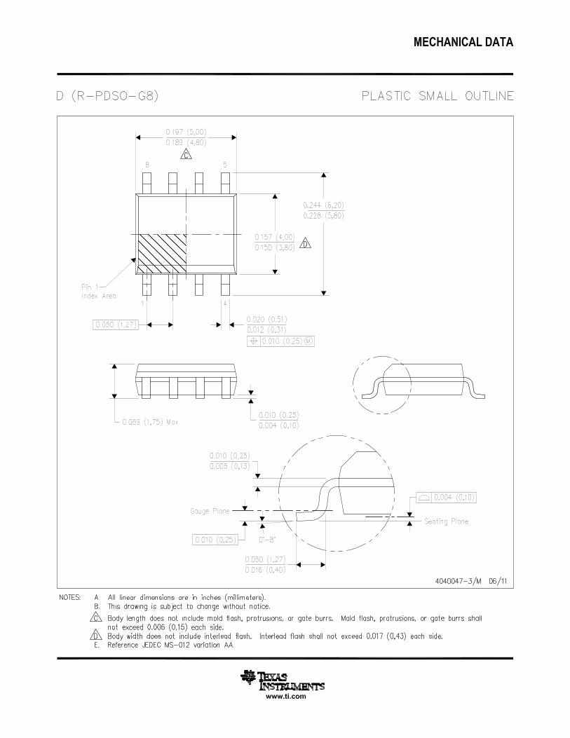


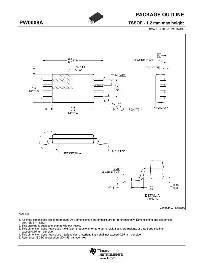
www.ti.com
PACKAGE OUTLINE
C
TYP6.66.2
1.2 MAX
6X 0.65
8X 0.300.19
2X1.95
0.150.05
(0.15) TYP
0 - 8
0.25GAGE PLANE
0.750.50
A
NOTE 3
3.12.9
BNOTE 4
4.54.3
4221848/A 02/2015
TSSOP - 1.2 mm max heightPW0008ASMALL OUTLINE PACKAGE
NOTES: 1. All linear dimensions are in millimeters. Any dimensions in parenthesis are for reference only. Dimensioning and tolerancing per ASME Y14.5M. 2. This drawing is subject to change without notice. 3. This dimension does not include mold flash, protrusions, or gate burrs. Mold flash, protrusions, or gate burrs shall not exceed 0.15 mm per side. 4. This dimension does not include interlead flash. Interlead flash shall not exceed 0.25 mm per side.5. Reference JEDEC registration MO-153, variation AA.
18
0.1 C A B
54
PIN 1 IDAREA
SEATING PLANE
0.1 C
SEE DETAIL A
DETAIL ATYPICAL
SCALE 2.800
www.ti.com
EXAMPLE BOARD LAYOUT
(5.8)
0.05 MAXALL AROUND
0.05 MINALL AROUND
8X (1.5)8X (0.45)
6X (0.65)
(R )TYP
0.05
4221848/A 02/2015
TSSOP - 1.2 mm max heightPW0008ASMALL OUTLINE PACKAGE
SYMM
SYMM
LAND PATTERN EXAMPLESCALE:10X
1
45
8
NOTES: (continued) 6. Publication IPC-7351 may have alternate designs. 7. Solder mask tolerances between and around signal pads can vary based on board fabrication site.
METALSOLDER MASKOPENING
NON SOLDER MASKDEFINED
SOLDER MASK DETAILSNOT TO SCALE
SOLDER MASKOPENING
METAL UNDERSOLDER MASK
SOLDER MASKDEFINED
www.ti.com
EXAMPLE STENCIL DESIGN
(5.8)
6X (0.65)
8X (0.45)8X (1.5)
(R ) TYP0.05
4221848/A 02/2015
TSSOP - 1.2 mm max heightPW0008ASMALL OUTLINE PACKAGE
NOTES: (continued) 8. Laser cutting apertures with trapezoidal walls and rounded corners may offer better paste release. IPC-7525 may have alternate design recommendations. 9. Board assembly site may have different recommendations for stencil design.
SYMM
SYMM
1
45
8
SOLDER PASTE EXAMPLEBASED ON 0.125 mm THICK STENCIL
SCALE:10X
IMPORTANT NOTICE
Texas Instruments Incorporated (TI) reserves the right to make corrections, enhancements, improvements and other changes to itssemiconductor products and services per JESD46, latest issue, and to discontinue any product or service per JESD48, latest issue. Buyersshould obtain the latest relevant information before placing orders and should verify that such information is current and complete.TI’s published terms of sale for semiconductor products (http://www.ti.com/sc/docs/stdterms.htm) apply to the sale of packaged integratedcircuit products that TI has qualified and released to market. Additional terms may apply to the use or sale of other types of TI products andservices.Reproduction of significant portions of TI information in TI data sheets is permissible only if reproduction is without alteration and isaccompanied by all associated warranties, conditions, limitations, and notices. TI is not responsible or liable for such reproduceddocumentation. Information of third parties may be subject to additional restrictions. Resale of TI products or services with statementsdifferent from or beyond the parameters stated by TI for that product or service voids all express and any implied warranties for theassociated TI product or service and is an unfair and deceptive business practice. TI is not responsible or liable for any such statements.Buyers and others who are developing systems that incorporate TI products (collectively, “Designers”) understand and agree that Designersremain responsible for using their independent analysis, evaluation and judgment in designing their applications and that Designers havefull and exclusive responsibility to assure the safety of Designers' applications and compliance of their applications (and of all TI productsused in or for Designers’ applications) with all applicable regulations, laws and other applicable requirements. Designer represents that, withrespect to their applications, Designer has all the necessary expertise to create and implement safeguards that (1) anticipate dangerousconsequences of failures, (2) monitor failures and their consequences, and (3) lessen the likelihood of failures that might cause harm andtake appropriate actions. Designer agrees that prior to using or distributing any applications that include TI products, Designer willthoroughly test such applications and the functionality of such TI products as used in such applications.TI’s provision of technical, application or other design advice, quality characterization, reliability data or other services or information,including, but not limited to, reference designs and materials relating to evaluation modules, (collectively, “TI Resources”) are intended toassist designers who are developing applications that incorporate TI products; by downloading, accessing or using TI Resources in anyway, Designer (individually or, if Designer is acting on behalf of a company, Designer’s company) agrees to use any particular TI Resourcesolely for this purpose and subject to the terms of this Notice.TI’s provision of TI Resources does not expand or otherwise alter TI’s applicable published warranties or warranty disclaimers for TIproducts, and no additional obligations or liabilities arise from TI providing such TI Resources. TI reserves the right to make corrections,enhancements, improvements and other changes to its TI Resources. TI has not conducted any testing other than that specificallydescribed in the published documentation for a particular TI Resource.Designer is authorized to use, copy and modify any individual TI Resource only in connection with the development of applications thatinclude the TI product(s) identified in such TI Resource. NO OTHER LICENSE, EXPRESS OR IMPLIED, BY ESTOPPEL OR OTHERWISETO ANY OTHER TI INTELLECTUAL PROPERTY RIGHT, AND NO LICENSE TO ANY TECHNOLOGY OR INTELLECTUAL PROPERTYRIGHT OF TI OR ANY THIRD PARTY IS GRANTED HEREIN, including but not limited to any patent right, copyright, mask work right, orother intellectual property right relating to any combination, machine, or process in which TI products or services are used. Informationregarding or referencing third-party products or services does not constitute a license to use such products or services, or a warranty orendorsement thereof. Use of TI Resources may require a license from a third party under the patents or other intellectual property of thethird party, or a license from TI under the patents or other intellectual property of TI.TI RESOURCES ARE PROVIDED “AS IS” AND WITH ALL FAULTS. TI DISCLAIMS ALL OTHER WARRANTIES ORREPRESENTATIONS, EXPRESS OR IMPLIED, REGARDING RESOURCES OR USE THEREOF, INCLUDING BUT NOT LIMITED TOACCURACY OR COMPLETENESS, TITLE, ANY EPIDEMIC FAILURE WARRANTY AND ANY IMPLIED WARRANTIES OFMERCHANTABILITY, FITNESS FOR A PARTICULAR PURPOSE, AND NON-INFRINGEMENT OF ANY THIRD PARTY INTELLECTUALPROPERTY RIGHTS. TI SHALL NOT BE LIABLE FOR AND SHALL NOT DEFEND OR INDEMNIFY DESIGNER AGAINST ANY CLAIM,INCLUDING BUT NOT LIMITED TO ANY INFRINGEMENT CLAIM THAT RELATES TO OR IS BASED ON ANY COMBINATION OFPRODUCTS EVEN IF DESCRIBED IN TI RESOURCES OR OTHERWISE. IN NO EVENT SHALL TI BE LIABLE FOR ANY ACTUAL,DIRECT, SPECIAL, COLLATERAL, INDIRECT, PUNITIVE, INCIDENTAL, CONSEQUENTIAL OR EXEMPLARY DAMAGES INCONNECTION WITH OR ARISING OUT OF TI RESOURCES OR USE THEREOF, AND REGARDLESS OF WHETHER TI HAS BEENADVISED OF THE POSSIBILITY OF SUCH DAMAGES.Unless TI has explicitly designated an individual product as meeting the requirements of a particular industry standard (e.g., ISO/TS 16949and ISO 26262), TI is not responsible for any failure to meet such industry standard requirements.Where TI specifically promotes products as facilitating functional safety or as compliant with industry functional safety standards, suchproducts are intended to help enable customers to design and create their own applications that meet applicable functional safety standardsand requirements. Using products in an application does not by itself establish any safety features in the application. Designers mustensure compliance with safety-related requirements and standards applicable to their applications. Designer may not use any TI products inlife-critical medical equipment unless authorized officers of the parties have executed a special contract specifically governing such use.Life-critical medical equipment is medical equipment where failure of such equipment would cause serious bodily injury or death (e.g., lifesupport, pacemakers, defibrillators, heart pumps, neurostimulators, and implantables). Such equipment includes, without limitation, allmedical devices identified by the U.S. Food and Drug Administration as Class III devices and equivalent classifications outside the U.S.TI may expressly designate certain products as completing a particular qualification (e.g., Q100, Military Grade, or Enhanced Product).Designers agree that it has the necessary expertise to select the product with the appropriate qualification designation for their applicationsand that proper product selection is at Designers’ own risk. Designers are solely responsible for compliance with all legal and regulatoryrequirements in connection with such selection.Designer will fully indemnify TI and its representatives against any damages, costs, losses, and/or liabilities arising out of Designer’s non-compliance with the terms and provisions of this Notice.
Mailing Address: Texas Instruments, Post Office Box 655303, Dallas, Texas 75265Copyright © 2017, Texas Instruments Incorporated
Recommended