1
Supplementary Information
Effects of line defects on the electronic and optical properties in strain-engineered WO3 thin films
Jing-ting Yang,a,b,‡ Chao Ma,a,‡ Chen Ge,*a Qinghua Zhang,a Jianyu Du,a Jiankun Li,a
Heyi Huang,a Meng He,a Can Wang,a Sheng Meng,a,c Lin Gu,a,b,c Huibin Lyu,a Guozhen
Yanga,b,c and Kuijuan Jin*a,b,c
a Beijing National Laboratory for Condensed Matter Physics, Institute of Physics,
Chinese Academy of Sciences, Beijing 100190, China
b School of Physical Sciences, University of Chinese Academy of Science, Beijing
100049, China
c Collaborative Innovation Center of Quantum Matter, Beijing 100871, China
‡ These authors contributed equally to this work.
*Corresponding Author: Chen Ge, [email protected]; Kuijuan Jin, [email protected]
Electronic Supplementary Material (ESI) for Journal of Materials Chemistry C.This journal is © The Royal Society of Chemistry 2017
2
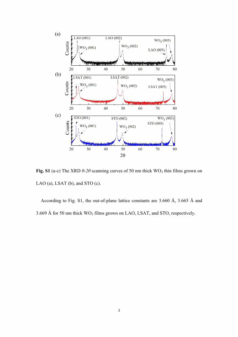
Fig. S1 (a-c) The XRD θ-2θ scanning curves of 50 nm thick WO3 thin films grown on
LAO (a), LSAT (b), and STO (c).
According to Fig. S1, the out-of-plane lattice constants are 3.660 Å, 3.665 Å and
3.669 Å for 50 nm thick WO3 films grown on LAO, LSAT, and STO, respectively.

3
Fig. S2 (a-c) The XRD patterns of WO3 thin films grown on LAO (a), LSAT (b), and
STO (c) substrates with different thickness. (d) Out-of-plane lattice parameters of WO3
vary with the film thickness for three substrates.
Fig. S2 (a-c) show the XRD θ-2θ scans of WO3 with different thickness grown on
LAO, LSAT and STO substrates, respectively. The (001) peaks of films grown on these
three substrates all slightly shift toward right with increasing thickness, indicating
smaller out-of-plane parameters in the thicker films as shown in Fig. S2 (d).

4
Fig. S3 AFM images of 20 nm thick WO3 films grown on (a) LAO (001), (b) LSAT
(001), and (c) STO (001). (d) The root-mean-square roughnesses and lattice mismatch
of thin films with different substrates.
Fig. S3 is the AFM images with size of 1.5 ×1.5 μm2 for 20 nm thick WO3 films
grown on (a) LAO (001), (b) LSAT (001), and (c) STO (001). The root-mean-square
(rms) roughnesses are 135, 276 and 400 pm for LAO, LSAT, and STO, respectively.
The small roughnesses indicate that all these films grow with atomically flat surfaces.
With an increasing lattice mismatch between film and substrate, the surface of film
become more roughly.

5
Fig. S4 XPS-spectrums of W 4f and 5p peaks for WO3 epitaxial films on LAO (a),
LSAT (b), and STO (c) substrates. Black symbols are the original data for XPS, and the
olive, magenta, navy fitting lines correspond to W 4f 7/2, 4f 5/2, and 5p 3/2 peaks,
respectively.
The chemical states of tungsten atoms for the as-deposited 50 nm thick WO3 films
grown on different substrates were evaluated by XPS as shown in Fig. S4. The black
symbols are the original data of XPS. The background signals is subtracted by Shirley
method. The olive, magenta, navy lines are the fitting curves corresponding to W 4f 7/2,
4f 5/2, and 5p 3/2 peaks, respectively. Referenced against C 1s at 284.6 eV, and the
binding energies of the W 4f 7/2 and W 4f 5/2 lines have been found at 35.3-35.6 eV and

6
37.4-37.7 eV, respectively. The parameters of W 4f spin-orbit separation ΔE (4f 5/2 -4f
7/2) in all films are all 2.14 eV, with intensities ratios eV. 𝐼4𝑓5/2 𝐼4𝑓7/2= 0.73 ± 0.1
These characters of W 4f correspond with WO3 in the earlier reports, S1-S4 which
indicating the existence of W6+ at the surface in each samples.

7
Fig. S5 STEM images of WO3 films grown on (a) LAO, and (b) LSAT, (c) STO
substrates viewed along the [100] direction. (d) The lattice mismatch (black symbol)
and thickness of line defects distribution (red symbol) of thin films grown on different
substrates.
Fig. S5 shows the spatial distribution of line defects in WO3 thin films. Fig. S5 (a-c)
revealed that line defects distribute only within ~6 nm away from the WO3/LAO
interface, ~7.6 nm away from the WO3/LSAT interface, and ~9 nm away from
WO3/STO interface. With larger lattice mismatch, WO3 thin films have more line
defects distributing in thicker region away from interface.

8
Fig. S6 Planar defects at the interface of film grown on (a) LSAT and (b) STO
substrates revealed by STEM.
Fig. S6 shows the planar defect appearing at interface of WO3/LSAT and WO3/STO
by STEM. These planar defects are in agreement with the recent report by Du et al. in
WO3/STO thin films.S5 Yellow arrows indicate the position of epitaxial interface. Red
circles indicate Al or Ta atoms in LSAT, and Ti atoms in STO. What’s more, the green
circles indicate W atoms. Four rows of W atoms are visible at the interface, compared
to five rows of that in the same field of view further away from the interface. It looks
like an intercalated column of tungsten atoms (marked by red arrow) in STEM image,
which compresses adjacent column, and allows smaller in-plane constants of adjacent

9
WO3 to accommodate near the interfaces. Actually, the planar defects make the tensile
strain releasing gradually, and propagate the lattice distortion deeply into the film.
The existence of the line defects and the planar defects can explain why the out-of-
plane lattice constant decreases with increasing film thickness (Fig. S2d). It is owing to
the line defects and planar defects, which both compress adjacent WO3 lattice and
stretch their out-of-plane lattice constants near the interface. Hence, the existence of
defects observed in the atomic scale is highly consistent with our XRD measurement.

10
Fig. S7 The smoothing of the DOS while introducing line defects. The definition of
“Wi” is the same as that in Fig. 3a in the manuscript. Compared to the defective unit
cells, the DOS of the defective-free unit cell has more remarkable peaks, especially
around -2 eV, -4 eV, and -5.5 eV.

11
Fig. S8 The lattice structures (upper panels) and corresponding 2D-contourmaps of
charge density distributions of the highest occupied band in the (0,2,0) plane (lower
panels). The definition of “Wi” and the contour levels (in B-G-R scale in all three
contourmaps) are the same as that in fig. 3 in the manuscript. The charge distribution
in (a) is much localized around the line defect at the center, which is in sharp contrast
to that in (b) and (c). In addition, the W3 becomes 7-coordinated by oxygen atoms, the
corresponding WO6-octahedron therefore deforms to a WO7-decahedron.
12
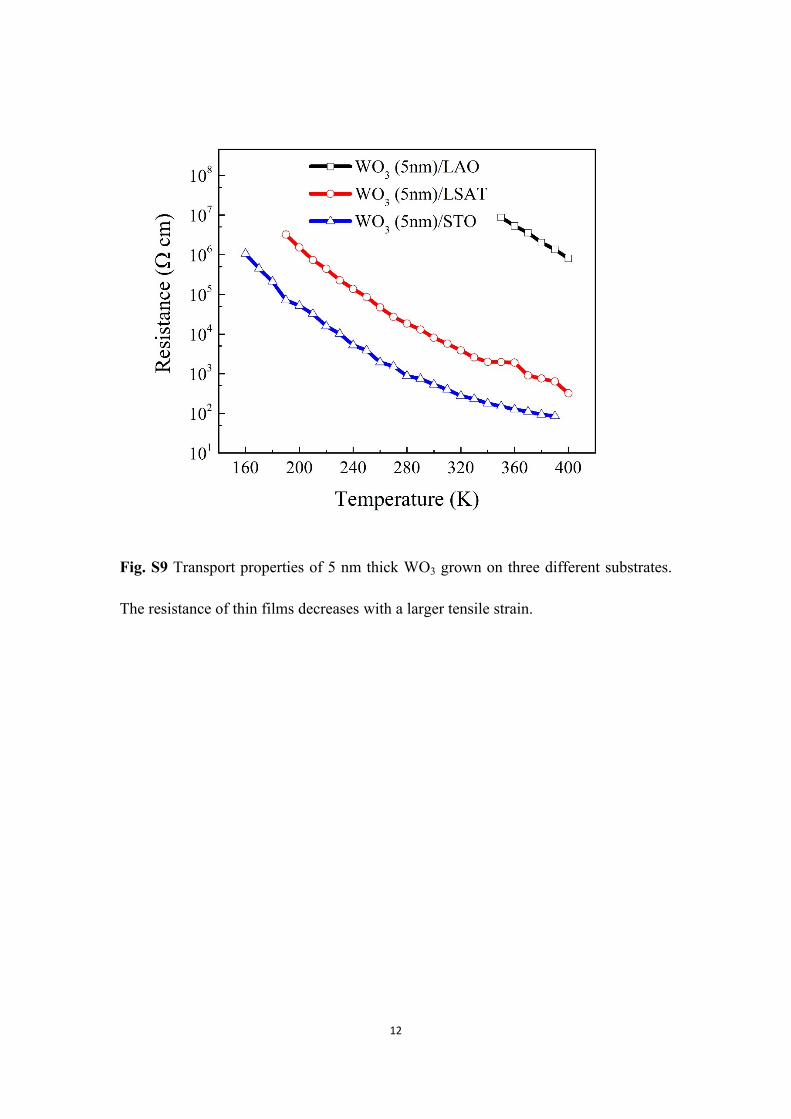
Fig. S9 Transport properties of 5 nm thick WO3 grown on three different substrates.
The resistance of thin films decreases with a larger tensile strain.

13
ReferencesS1 T. H. Fleisch, G. J. Mains, J. Chem. Phys., 1982, 76, 780.
S2 P. Charton, L. Gengembre, P. Armand, J. Solid State Chem., 2002, 168, 175.
S3 A. P. Shpak, A. M. Korduban, M. M. Medvedskij, V. O. Kandyba, J. Electron.
Spectrosc. Relat. Phenom., 2007, 156, 172.
S4 R. Azimirad, N. Naseri, O. Akhavan, A. Z. Moshfegh, J. Phys. D: Appl. Phys., 2007,
40, 1134.
S5 Y. Du, M. Gu, T. Varga, C. Wang, M. E. Bowden, S. A. Chambers, ACS Appl.
Mater. Interfaces, 2014, 6, 14253.
Recommended