MemSpeed®3.0 & MemSolid®3.0 Technical White Paper
An In-depth Look at Consistent High Performance and Reliability
v3.1
Memblaze® PBlaze5
Technical White Paper | MemSolid®3.0 & MemSpeed®3.0 Beijing Memblaze Technology Co., Ltd. 2
Contents
EXECUTIVE SUMMARY 6
INDUSTRY TREND 6
PCIe SSD - Mainstream in Data Center Applications 6
Outstanding performance removes I/O bottleneck that plagues modern-day data centers 6 PCIe SSD is more economical than traditional storage technologies 7 Higher revenue proportion with PCIe SSD 7
NVMeTM SSD is the Future 7
SSD standard evolution in enterprise market 7 NVMe benefits 8
Why New Generation PBlaze5 Chooses 3D NAND? 9
Larger capacity, NAND reliability and cost optimization 9 Mainly evolutions on NAND, capacity, performance and features of PBlaze5 10
OPTIMIZING PERFORMANCE WITH MEMSPEED®3.0 11
Multi-Plane Operation 11
A brief introduction to NAND inside 11 Simultaneously program multi-plane to improve performance 11
Multi-core Computing 13
Achieving energy-efficient performance with multiple processor cores 13 New flash channel cores realize full flexibility to support NAND with advanced features 13
Memblaze® PBlaze5
Technical White Paper | MemSolid®3.0 & MemSpeed®3.0 Beijing Memblaze Technology Co., Ltd. 3
Hardware Multi-Q 13
Why adopts hardware multi-Q? 13 How does multi-Q work? 13
Adaptive Smooth Technology 15
What is “Latency Jitter”? QoS? 15 Negative feedback like adaptive smooth technology 15
Flash Channel QoS 15
Ensure QoS via priority scheduling 15 Further reduce read latency by implementing Priority Queue Management 16
High Performance FTL 17
What is FTL? 17 Improve performance and wear Leveling with global FTL 17
TRIM 17
Improve write performance and endurance 17
PROVEN DATA RELIABILITY WITH MEMSOLID®3.0 19
Strong Error Correcting Code - LDPC 20
Why LDPC? 20 Powerful soft-decision decoding LDPC 20 LDPC in NAND 21
Full Data Path Protection 21
Full Data Path Protection 21
Data Path End-to-End Protection 22
Unavoidability silent data error & uncorrectable data error 22 Data Path End-to-End Protection against silent data corruption 22
Enhanced Power Failure Protection 23
Why requires power failure protection on SSD? 23 Enhanced power failure protection on PBlaze5 with capacitor health monitor 23 Further ensure data integrity via Erase Cancellation 24
PCI Express ECRC Protection 25
Understanding PCIe Link 25 ECRC generation and ECRC check at transaction layer 25
Metadata Protection 26
High write speed and endurance of pSLC mode 26 Multi-copy for redundancy 27
RAID Protection 27
Memblaze® PBlaze5
Technical White Paper | MemSolid®3.0 & MemSpeed®3.0 Beijing Memblaze Technology Co., Ltd. 4
Guarantee high data reliability with dynamic RAID5 protection among dies 27
Read Retry 28
Why Read Retry is required? 28 Read Level Self-Calibration 28
Read Disturb Protection 29
What is Read Disturb? 29 Move frequently accessed data with dynamical read count threshold setting 29
Program Disturb Protection 30
What is Program Disturb? 30 Randomization to realize program protection 30
Data Retention Enhanced 30
P/E, temperature influence on flash Data Retention 30 Move data has not accessed for a certain time to enhance Data Retention 31
Fast Recovery 31
Shortening the system recovery time with on-demand recovery 31
High Temperature Protection 32
Dynamical thermal monitoring and throttling 32
Wear leveling 33
Evenly spread hot data with dynamic wear leveling 33 Moves stale cold data by static wear leveling 33
S.M.A.R.T 34
Self-Monitoring, Analysis and Reporting Technology 34 Standard SMART attributes 34
PBLAZE5 PROVIDES RICH ENTERPRISE-LEVEL FEATURES 35
Whole Disk Encryption with AES-XTS 256-bit 35
Superior data protection with AES-XTS 35 How does AES-XTS work? 36
Crypto erase 37
More secure guard with Cryptographic Erase 37
Firmware Signature 37
Firmware signature to avoid malicious tampering and attackers 37
Dual Port (Only for U.2) 38
Redundancy link delivers high availability 38
Multiple Namespace 38
Memblaze® PBlaze5
Technical White Paper | MemSolid®3.0 & MemSpeed®3.0 Beijing Memblaze Technology Co., Ltd. 5
Flexible utilization of multiple namespace 38
Flexible Power Management 39
Selectable power model for temperature control ecosystem 39
SUMMARY 40
REFERENCE 41
CONTRIBUTION 42
REVISION HISTORY 42
ABOUT MEMBLAZE 43
Memblaze® PBlaze5
Technical White Paper | MemSolid®3.0 & MemSpeed®3.0 Beijing Memblaze Technology Co., Ltd. 6
Executive Summary
There are a number of workloads that require increased performance, both in terms of higher IOPS and consistent low latency to read and write data, such as Online Transaction Processing (OLTP), Online Analytical Processing (OLAP), High Performance Computing (HPC), Cloud/hyper scale computing, Virtualized computing. As a result, SSDs are becoming a vital part of today's datacenter infrastructure as a mechanism to store and access the growing amount of data more quickly and efficiently. Besides the high performance, in some applications, for example e-commerce, data protection is treated critical important. As the data error or corruption may result in incorrect orders, sensitive or confidential information leakage when sending over via internet or attacked by hackers. Thus, comprehensive data protection technology is required to implement in different level on enterprise-class Solid State Drive.
PBlaze5 is Memblaze’s 5th generation Enterprise-level Solid State Drive series which fully compliant with NVMe1.2a standard, adopts industry-leading 3D NAND and provides larger capacity up to 11 TB, comes in both HHHL and 2.5” U.2 form factor for data center and enterprise applications. Coupled with MemSpeed®3.0 and MemSolid®3.0 technologies set, unleash Memblaze PBlaze5 - NVMeTM based Enterprise-class SSD to provide consistent superior IOPS, throughput, sustained low latency, variety of features and indispensable reliability for the most demanding data center applications.
This paper will help to lay down some of the industry trends, find out why Memblaze PBlaze5 can show such outstanding performance and share approaches implemented on PBlaze5 to minimize the pervasive data corruption risk and heighten the user experience.
Industry Trend
PCIe SSD - Mainstream in Data Center Applications
Outstanding performance removes I/O bottleneck that plagues modern-day data centers
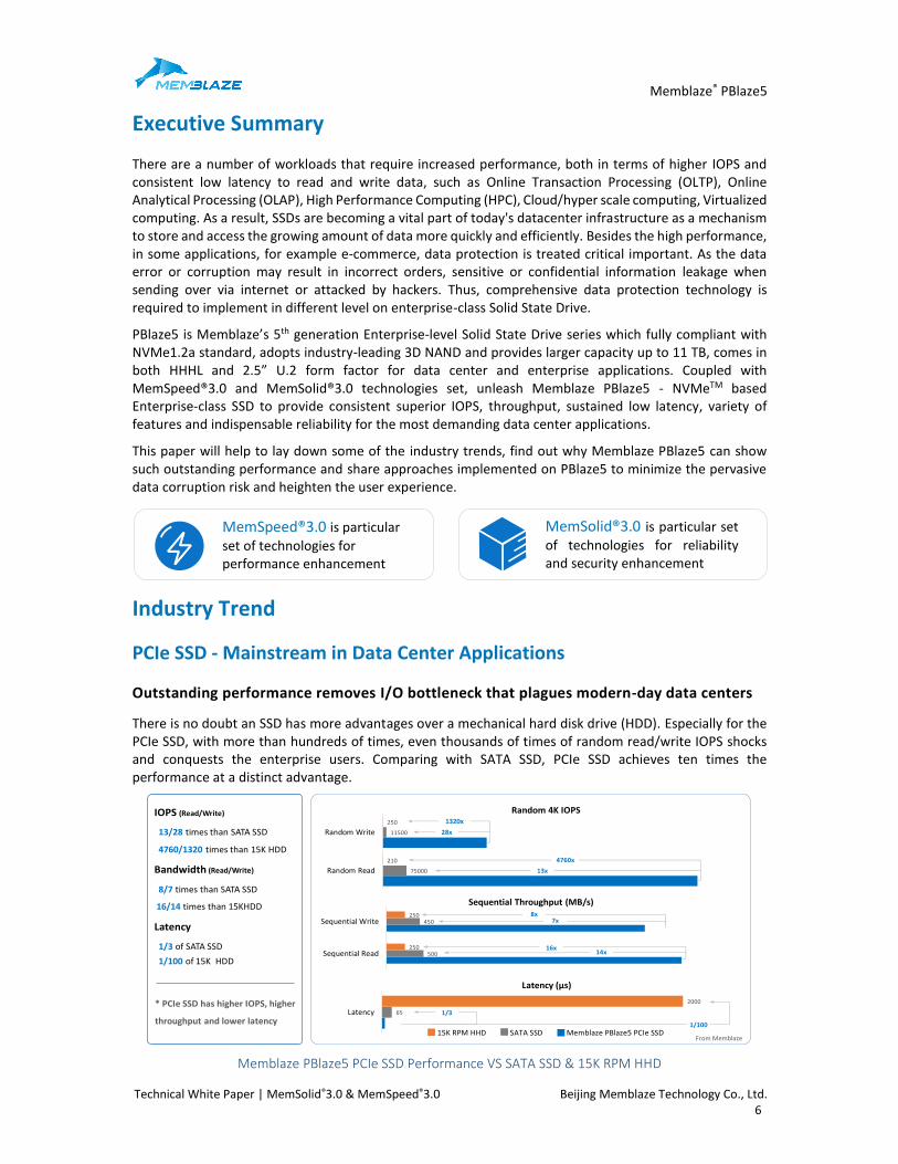
There is no doubt an SSD has more advantages over a mechanical hard disk drive (HDD). Especially for the PCIe SSD, with more than hundreds of times, even thousands of times of random read/write IOPS shocks and conquests the enterprise users. Comparing with SATA SSD, PCIe SSD achieves ten times the performance at a distinct advantage.
75000
11500
210
250
Random Read
Random Write
Random 4K IOPS1320x
65
2000
Latency
Latency (μs)
15K RPM HHD SATA SSD Memblaze PBlaze5 PCIe SSD
1/3
1/100
IOPS (Read/Write)
13/28 times than SATA SSD
4760/1320 times than 15K HDD
Bandwidth (Read/Write)
8/7 times than SATA SSD
16/14 times than 15KHDD
Latency
1/3 of SATA SSD
1/100 of 15K HDD
* PCIe SSD has higher IOPS, higher
throughput and lower latency
From Memblaze
13x
28x
4760x
500
450
250
250
Sequential Read
Sequential Write
Sequential Throughput (MB/s)
7x8x
14x16x
Memblaze PBlaze5 PCIe SSD Performance VS SATA SSD & 15K RPM HHD
MemSpeed®3.0 is particular
set of technologies for performance enhancement
MemSolid®3.0 is particular set
of technologies for reliability and security enhancement
Memblaze® PBlaze5
Technical White Paper | MemSolid®3.0 & MemSpeed®3.0 Beijing Memblaze Technology Co., Ltd. 7
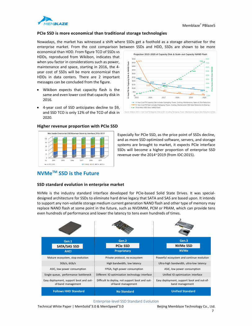
PCIe SSD is more economical than traditional storage technologies
Nowadays, the market has witnessed a shift where SSDs get a foothold as a storage alternative for the enterprise market. From the cost comparison between SSDs and HDD, SSDs are shown to be more economical than HDD. From figure TCO of SSDs vs HDDs, reproduced from Wikibon, indicates that when you factor in considerations such as power, maintenance and space, starting in 2016, the 4-year cost of SSDs will be more economical than HDDs in data centers. There are 2 important messages can be concluded from the figure.
• Wikibon expects that capacity flash is the same and even lower cost that capacity disk in 2016.
• 4-year cost of SSD anticipates decline to $9, and SSD TCO is only 12% of the TCO of disk in 2020.
Higher revenue proportion with PCIe SSD
Especially for PCIe SSD, as the price point of SSDs decline, and as more SSD optimized software, servers, and storage systems are brought to market, it expects PCIe interface SSDs will become a higher proportion of enterprise SSD revenue over the 2014~2019 (from IDC:2015).
NVMeTM SSD is the Future
SSD standard evolution in enterprise market
NVMe is the industry standard interface developed for PCIe-based Solid State Drives. It was special-designed architecture for SSDs to eliminate hard drive legacy that SATA and SAS are based upon. It intends to support any non-volatile storage medium current generation NAND flash and other type of memory may replace NAND flash at some point in the future, such as NVDIMM, PCM or PRAM, which can provide tens even hundreds of performance and lower the latency to tens even hundreds of times.
统一标准没有标准沿用机械硬盘标准
Mature ecosystem, stop evolution Private protocol, no ecosystem Powerful ecosystem and continue evolution
3Gb/s, 6Gb/s High bandwidth, low latency Ultra-high bandwidth, ultra-low latency
ASIC, low power consumption FPGA, high power consumption ASIC, low power consumption
Single queue, performance bottleneck Different IO optimization technology interface Unified IO optimization interface
Easy deployment, support boot and out-of-band management
Difficult to deploy, not support boot and out-of-band management
Easy deployment, support boot and out-of-band management
Gen.1
SATA/SAS SSD
AHCI
Follows HHD Standard No Standard Unified Standard
Gen.2
PCIe SSD
Proprietary
Gen.3
NVMe SSD
NVMe
Enterprise-level SSD Standard Evolution
$237
$169$140
$113$91
$74
$470
$151
$62
$30 $16 $9-50%
19%
139%
300%
498%
732%
-100%
0%
100%
200%
300%
400%
500%
600%
700%
800%
$0
$50
$100
$150
$200
$250
$300
$350
$400
$450
$500
2015 2016 2017 2018 2019 20204-Y
ear/
TB
fo
r C
ap
aci
ty D
isk &
NA
ND
Fla
sh
Projection 2015-2020 of Capacity Disk & Scale-out Capacity NAND Flash
4-Year Cost/TB Capacity Disk includes Packaging, Power, Cooling, Maintenance, Space & Disk Reduction
4-Year Cost/TB Flash includes Packaging, Power, Cooling, Maintenance, SSD Date Reduction & Sharing
Price Ratio HDD Disk: NAND Flash
Pri
ce R
ati
o H
DD
Dis
k:N
AN
D
Source: Wikbon 2015 4-Year Cost/TB Magnetic Disk & SSD. including Packaging, Power, Maintenance, Space, Data Reduction & Data
Memblaze® PBlaze5
Technical White Paper | MemSolid®3.0 & MemSpeed®3.0 Beijing Memblaze Technology Co., Ltd. 8
NVMe benefits
There are four key benefits that NVMe brings to the data centers implementing SSD technology.
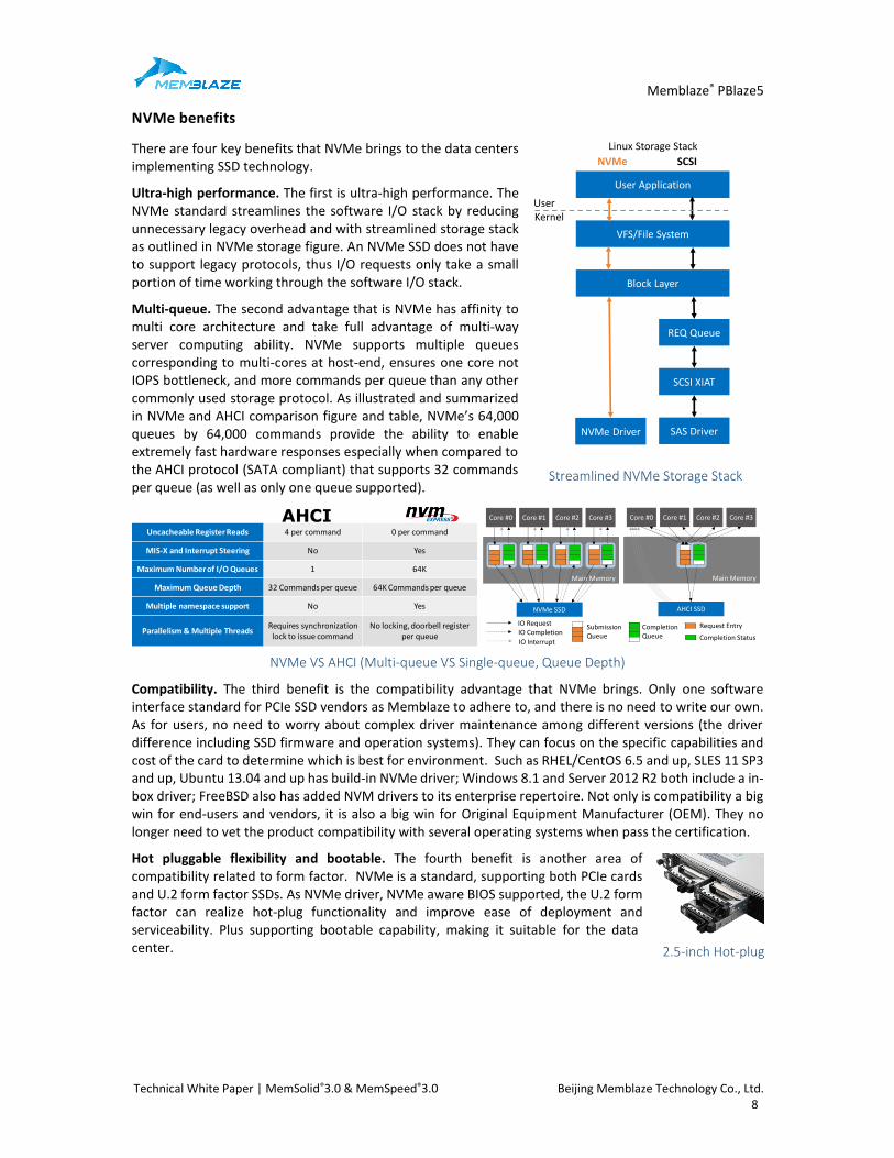
Ultra-high performance. The first is ultra-high performance. The NVMe standard streamlines the software I/O stack by reducing unnecessary legacy overhead and with streamlined storage stack as outlined in NVMe storage figure. An NVMe SSD does not have to support legacy protocols, thus I/O requests only take a small portion of time working through the software I/O stack.
Multi-queue. The second advantage that is NVMe has affinity to multi core architecture and take full advantage of multi-way server computing ability. NVMe supports multiple queues corresponding to multi-cores at host-end, ensures one core not IOPS bottleneck, and more commands per queue than any other commonly used storage protocol. As illustrated and summarized in NVMe and AHCI comparison figure and table, NVMe’s 64,000 queues by 64,000 commands provide the ability to enable extremely fast hardware responses especially when compared to the AHCI protocol (SATA compliant) that supports 32 commands per queue (as well as only one queue supported).
Uncacheable Register Reads 4 per command 0 per command
MIS-X and Interrupt Steering No Yes
Maximum Number of I/O Queues 1 64K
Maximum Queue Depth 32 Commands per queue 64K Commands per queue
Multiple namespace support No Yes
Parallelism & Multiple ThreadsRequires synchronization lock to issue command
No locking, doorbell register per queue
AHCI
Core #0
Main Memory
NVMe SSD AHCI SSD
Core #1 Core #2 Core #3 Core #0
Main Memory
Core #1 Core #2 Core #3
IO RequestIO Completion
IO Interrupt
Submission Queue
Completion Queue Completion Status
Request Entry
NVMe VS AHCI (Multi-queue VS Single-queue, Queue Depth)
Compatibility. The third benefit is the compatibility advantage that NVMe brings. Only one software interface standard for PCIe SSD vendors as Memblaze to adhere to, and there is no need to write our own. As for users, no need to worry about complex driver maintenance among different versions (the driver difference including SSD firmware and operation systems). They can focus on the specific capabilities and cost of the card to determine which is best for environment. Such as RHEL/CentOS 6.5 and up, SLES 11 SP3 and up, Ubuntu 13.04 and up has build-in NVMe driver; Windows 8.1 and Server 2012 R2 both include a in-box driver; FreeBSD also has added NVM drivers to its enterprise repertoire. Not only is compatibility a big win for end-users and vendors, it is also a big win for Original Equipment Manufacturer (OEM). They no longer need to vet the product compatibility with several operating systems when pass the certification.
Hot pluggable flexibility and bootable. The fourth benefit is another area of compatibility related to form factor. NVMe is a standard, supporting both PCIe cards and U.2 form factor SSDs. As NVMe driver, NVMe aware BIOS supported, the U.2 form factor can realize hot-plug functionality and improve ease of deployment and serviceability. Plus supporting bootable capability, making it suitable for the data center.
Streamlined NVMe Storage Stack
2.5-inch Hot-plug
User Application
VFS/File System
Block Layer
REQ Queue
SCSI XIAT
SAS DriverNVMe Driver
UserKernel
NVMe SCSI
Linux Storage Stack
Memblaze® PBlaze5
Technical White Paper | MemSolid®3.0 & MemSpeed®3.0 Beijing Memblaze Technology Co., Ltd. 9
Why New Generation PBlaze5 Chooses 3D NAND?
Larger capacity, NAND reliability and cost optimization
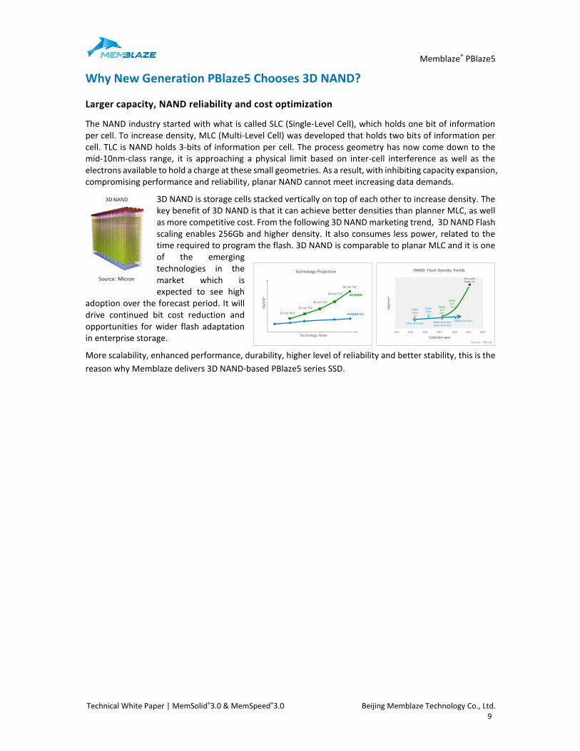
The NAND industry started with what is called SLC (Single-Level Cell), which holds one bit of information per cell. To increase density, MLC (Multi-Level Cell) was developed that holds two bits of information per cell. TLC is NAND holds 3-bits of information per cell. The process geometry has now come down to the mid-10nm-class range, it is approaching a physical limit based on inter-cell interference as well as the electrons available to hold a charge at these small geometries. As a result, with inhibiting capacity expansion, compromising performance and reliability, planar NAND cannot meet increasing data demands.
3D NAND is storage cells stacked vertically on top of each other to increase density. The key benefit of 3D NAND is that it can achieve better densities than planner MLC, as well as more competitive cost. From the following 3D NAND marketing trend, 3D NAND Flash scaling enables 256Gb and higher density. It also consumes less power, related to the time required to program the flash. 3D NAND is comparable to planar MLC and it is one of the emerging technologies in the market which is expected to see high
adoption over the forecast period. It will drive continued bit cost reduction and opportunities for wider flash adaptation in enterprise storage.
More scalability, enhanced performance, durability, higher level of reliability and better stability, this is the
reason why Memblaze delivers 3D NAND-based PBlaze5 series SSD.
Technology Projection
Technology Node
GB
/CM
2
32-tier MLC
32-tier TLC
48-tier TLC
64-tier TLC
96-tier TLC
3D NAND
PLANAR TLC
NAND Flash Density Trends
Source – Micron
64Gb 19nm MLC
128Gb20nmTLC
128Gb20nmTLC
128Gb24-TMLC
128Gb32-TTLC
This works768Gb TLC
128Gb 16nm MLC64Gb 16nm MLC
128Gb 15nm MLC
2011 2012 2013 2014 2015 2016 2017
Gb
/mm
2
Calendar year
Memblaze® PBlaze5
Technical White Paper | MemSolid®3.0 & MemSpeed®3.0 Beijing Memblaze Technology Co., Ltd. 10
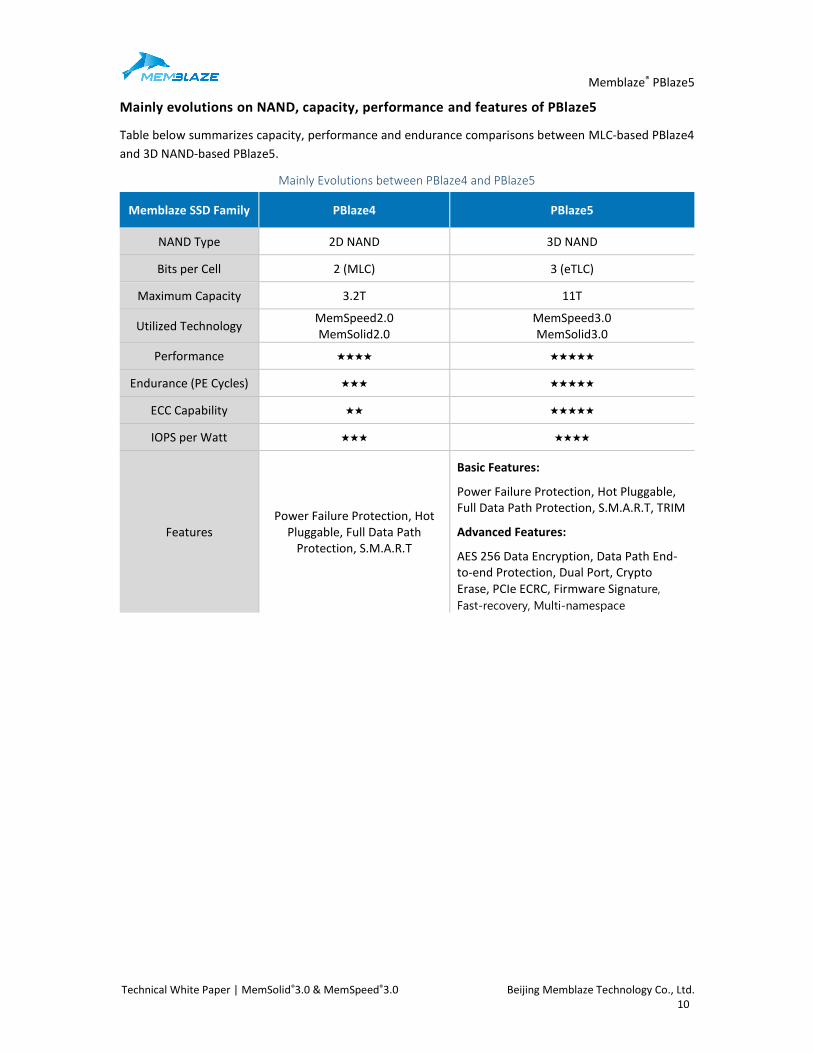
Mainly evolutions on NAND, capacity, performance and features of PBlaze5
Table below summarizes capacity, performance and endurance comparisons between MLC-based PBlaze4
and 3D NAND-based PBlaze5.
Mainly Evolutions between PBlaze4 and PBlaze5
Memblaze SSD Family PBlaze4 PBlaze5
NAND Type 2D NAND 3D NAND
Bits per Cell 2 (MLC) 3 (eTLC)
Maximum Capacity 3.2T 11T
Utilized Technology MemSpeed2.0 MemSolid2.0
MemSpeed3.0 MemSolid3.0
Performance ★★★★ ★★★★★
Endurance (PE Cycles) ★★★ ★★★★★
ECC Capability ★★ ★★★★★
IOPS per Watt ★★★ ★★★★
Features Power Failure Protection, Hot
Pluggable, Full Data Path Protection, S.M.A.R.T
Basic Features:
Power Failure Protection, Hot Pluggable, Full Data Path Protection, S.M.A.R.T, TRIM
Advanced Features:
AES 256 Data Encryption, Data Path End-to-end Protection, Dual Port, Crypto Erase, PCIe ECRC, Firmware Signature,
Fast-recovery, Multi-namespace
Memblaze® PBlaze5
Technical White Paper | MemSolid®3.0 & MemSpeed®3.0 Beijing Memblaze Technology Co., Ltd. 11
Optimizing Performance with MemSpeed®3.0
We have taken a look at a few Memblaze-built solid state drives over the years and found them all to be
relatively strong performers, thus the benefits from MemSpeed® which is the technology set for
performance enhancement. On PBlaze5, MemSpeed® fully upgrade from 2.0 to 3.0, and you can find out
coverage of the MemSpeed®3.0 from following Table. This the reason why Memblaze PBlaze5 can be an
ultra-fast data center SSD.
MemSpeed® Technology Improvements between PBlaze4 and PBlaze5
MemSpeed® * PBlaze4 PBlaze5
MemSpeed®2.0 MemSpeed®3.0
Multi-plane Operation ✓
Write Back Cache ✓ ✓
High Performance FTL ✓ ✓
Flash Channel QoS ✓ Priority Queue Management
Adaptive Smooth Technology ✓ ✓
Multi-core Computing Multi-core (16 cores) 16 CPU cores + 16 Flash Channel
Controller Cores
Hardware Multi-Q ✓ ✓
TRIM ✓ ✓
Multi-Plane Operation
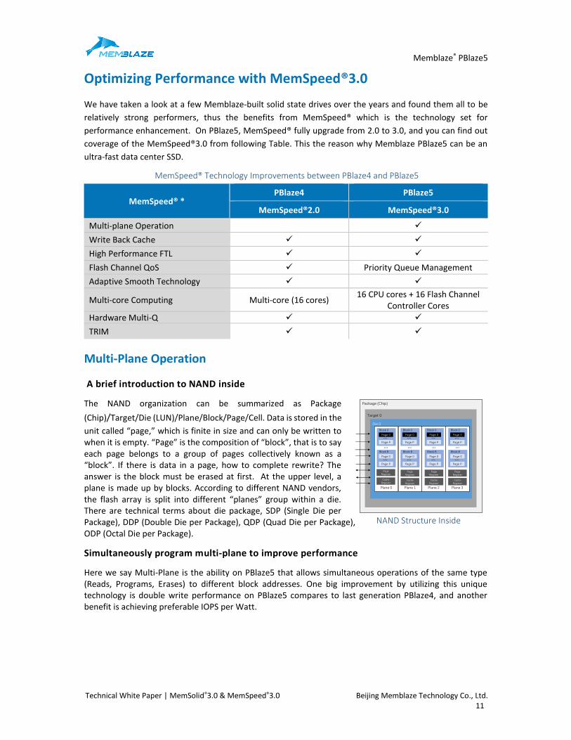
A brief introduction to NAND inside
The NAND organization can be summarized as Package
(Chip)/Target/Die (LUN)/Plane/Block/Page/Cell. Data is stored in the
unit called “page,” which is finite in size and can only be written to when it is empty. “Page” is the composition of “block”, that is to say each page belongs to a group of pages collectively known as a “block”. If there is data in a page, how to complete rewrite? The answer is the block must be erased at first. At the upper level, a plane is made up by blocks. According to different NAND vendors, the flash array is split into different “planes” group within a die. There are technical terms about die package, SDP (Single Die per Package), DDP (Double Die per Package), QDP (Quad Die per Package), ODP (Octal Die per Package).
Simultaneously program multi-plane to improve performance
Here we say Multi-Plane is the ability on PBlaze5 that allows simultaneous operations of the same type (Reads, Programs, Erases) to different block addresses. One big improvement by utilizing this unique technology is double write performance on PBlaze5 compares to last generation PBlaze4, and another benefit is achieving preferable IOPS per Watt.
Package (Chip)
Target 0
Die 0
Plane 0 Plane 1 Plane 2 Plane 3
Block 0
Page 0
Page P
…
…Block B
Page 0
Page P
…
Block 0
Page 0
Page P
…
…Block B
Page 0
Page P
…
Block 0
Page 0
Page P
…
…Block B
Page 0
Page P
…
Block 0
Page 0
Page P
…
…Block B
Page 0
Page P
…
Page Register
Cache Register
Page Register
Cache Register
Page Register
Cache Register
Page Register
Cache Register
NAND Structure Inside
Memblaze® PBlaze5
Technical White Paper | MemSolid®3.0 & MemSpeed®3.0 Beijing Memblaze Technology Co., Ltd. 12
PackagePackage
Target 0
Die 0
Plane 0 Plane 1 Plane 2 Plane 31
Target 1
Die 0
Plane 0 Plane 1 Plane 2 Plane 32
Target 2
Die 0
Plane 0 Plane 1 Plane 2 Plane 33
Target 3
Die 0
Plane 0 Plane 1 Plane 2 Plane 34
16K 16K 16K 16K
Target 0
Die 0
Plane 0 Plane 1 Plane 2 Plane 3
Target 1
Die 0
Plane 0 Plane 1 Plane 2 Plane 3
Target 2
Die 0
Plane 0 Plane 1 Plane 2 Plane 3
Target 3
Die 0
Plane 0 Plane 1 Plane 2 Plane 3
1 2 3 4
64K User Data:
Page
Single Plane Write Multi-plane Write
Writing order: 4 3 2 1
· · ·
Die 0
Plane 0 Plane 1 Plane 2 Plane 3
Block 0
Page 0
Page P
…
…Block B
Page 0
Page P
…
Block 0
Page 0
Page P
…
…Block B
Page 0
Page P
…
Block 0
Page 0
Page P
…
…Block B
Page 0
Page P
…
Block 0
Page 0
Page P
…
…Block B
Page 0
Page P
…
Page Register
Cache Register
Page Register
Cache Register
Page Register
Cache Register
Page Register
Cache Register
Package
DieTarget
Plane
Block
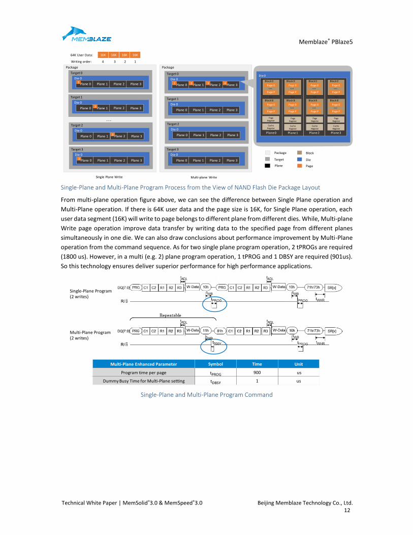
Single-Plane and Multi-Plane Program Process from the View of NAND Flash Die Package Layout
From multi-plane operation figure above, we can see the difference between Single Plane operation and
Multi-Plane operation. If there is 64K user data and the page size is 16K, for Single Plane operation, each
user data segment (16K) will write to page belongs to different plane from different dies. While, Multi-plane
Write page operation improve data transfer by writing data to the specified page from different planes
simultaneously in one die. We can also draw conclusions about performance improvement by Multi-Plane
operation from the command sequence. As for two single plane program operation, 2 tPROGs are required
(1800 us). However, in a multi (e.g. 2) plane program operation, 1 tPROG and 1 DBSY are required (901us).
So this technology ensures deliver superior performance for high performance applications.
Multi-Plane Program(2 writes)
Single-Plane Program(2 writes)
Multi-Plane Enhanced Parameter Symbol Time Unit
Program time per page tPROG 900 us
Dummy Busy Time for Multi-Plane setting tDBSY 1 us
Single-Plane and Multi-Plane Program Command
Memblaze® PBlaze5
Technical White Paper | MemSolid®3.0 & MemSpeed®3.0 Beijing Memblaze Technology Co., Ltd. 13
Multi-core Computing
Achieving energy-efficient performance with multiple processor cores
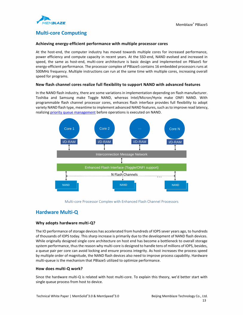
At the host-end, the computer industry has moved towards multiple cores for increased performance, power efficiency and compute capacity in recent years. At the SSD-end, NAND evolved and increased in speed, the same as host-end, multi-core architecture is basic design and implemented on PBlaze5 for energy-efficient performance. The processor complex of PBlaze5 contains 16 embedded processors runs at 500MHz frequency. Multiple instructions can run at the same time with multiple cores, increasing overall speed for programs.
New flash channel cores realize full flexibility to support NAND with advanced features
In the NAND flash industry, there are some variations in implementation depending on flash manufacturer. Toshiba and Samsung make Toggle NAND, whereas Intel/Micron/Hynix make ONFI NAND. With programmable flash channel processor cores, enhances flash interface provides full flexibility to adopt variety NAND flash type, meantime to implement advanced NAND features, such as to improve read latency, realizing priority queue management before operations is executed on NAND.
Multi-core Processor Complex with Enhanced Flash Channel Processors
Hardware Multi-Q
Why adopts hardware multi-Q?
The IO performance of storage devices has accelerated from hundreds of IOPS sever years ago, to hundreds of thousands of IOPS today. This sharp increase is primarily due to the development of NAND flash devices. While originally designed single core architecture on host end has become a bottleneck to overall storage system performance, thus the reason why multi-core is designed to handle tens of millions of IOPS, besides, a queue pair per core can avoid locking and ensure process integrity. As host increases the process speed by multiple order of magnitude, the NAND flash devices also need to improve process capability. Hardware multi-queue is the mechanism that PBlaze5 utilized to optimize performance.
How does multi-Q work?
Since the hardware multi-Q is related with host multi-core. To explain this theory, we’d better start with single queue process from host to device.
Core 1 Core 2 Core N···
I/D-RAM I/D-RAM
Interconnection Message Network
Enhanced Flash Interface (Toggle/ONFI support)
I/D-RAM I/D-RAM
· · ·N Flash Channels
NANDNAND
NANDNAND
NANDNAND
Memblaze® PBlaze5
Technical White Paper | MemSolid®3.0 & MemSpeed®3.0 Beijing Memblaze Technology Co., Ltd. 14
Host
Core 0
Device Controller
Submission Queue
CompletionQueue
Core 1Submission
QueueCompletion
Queue
Core NSubmission
QueueCompletion
Queue
···
Submission Queue Engines
Process Unit 1
Completion Queue Engines
Process Unit 2
Process Unit 3
···Process Unit N
1 Host Writes Command to Submission Queue Entry
Host Writes Doorbell
Signaling New Command
2
Fetch Command
3
4Controller Executes
Command
Controller Writes Completion Entry5
Controller Generates Interrupt
6
7 Host Process Completion Entry
8
Host Writes Doorbell To
Release Completion Entry
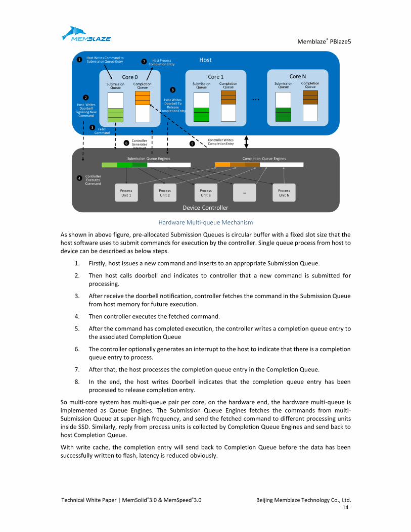
Hardware Multi-queue Mechanism
As shown in above figure, pre-allocated Submission Queues is circular buffer with a fixed slot size that the host software uses to submit commands for execution by the controller. Single queue process from host to device can be described as below steps.
1. Firstly, host issues a new command and inserts to an appropriate Submission Queue.
2. Then host calls doorbell and indicates to controller that a new command is submitted for processing.
3. After receive the doorbell notification, controller fetches the command in the Submission Queue from host memory for future execution.
4. Then controller executes the fetched command.
5. After the command has completed execution, the controller writes a completion queue entry to the associated Completion Queue
6. The controller optionally generates an interrupt to the host to indicate that there is a completion queue entry to process.
7. After that, the host processes the completion queue entry in the Completion Queue.
8. In the end, the host writes Doorbell indicates that the completion queue entry has been processed to release completion entry.
So multi-core system has multi-queue pair per core, on the hardware end, the hardware multi-queue is implemented as Queue Engines. The Submission Queue Engines fetches the commands from multi-Submission Queue at super-high frequency, and send the fetched command to different processing units inside SSD. Similarly, reply from process units is collected by Completion Queue Engines and send back to host Completion Queue.
With write cache, the completion entry will send back to Completion Queue before the data has been successfully written to flash, latency is reduced obviously.
Memblaze® PBlaze5
Technical White Paper | MemSolid®3.0 & MemSpeed®3.0 Beijing Memblaze Technology Co., Ltd. 15
Adaptive Smooth Technology
What is “Latency Jitter”? QoS?
“Latency Jitter” is an important indicator of the enterprise level flash storage. It is a phenomenon that during read and write operations, appears I0 latency exceeds several times or dozens of times that of normal latency. How it appears? The major reason is that the “Garbage Collection” (GC) operation is ongoing during flash device exchanges data with host. GC capability affects normal operations and thereby produce IO latency jitter. The Latency jitter of SSD can be quantified via Quality of Service (QoS) parameter, which is the requirement that a given application complete all requested processes under steady and consistent performance within a specified time limit. Usually, SSD QoS is given as a maximum response time under the certain confidence level of 99% or 99.99% (“2 nines or 4 nines” of confidence level).
How to optimize? Adaptive Smooth Technology is designed on PBlaze5, with Scheduler Process together to reduce the latency jitter.
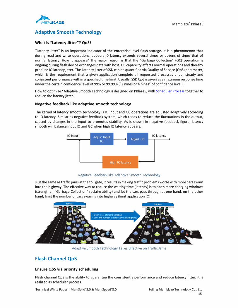
Negative feedback like adaptive smooth technology
The kernel of latency smooth technology is IO input and GC operations are adjusted adaptively according to IO latency. Similar as negative feedback system, which tends to reduce the fluctuations in the output, caused by changes in the input to promotes stability. As is shown in negative feedback figure, latency smooth will balance input IO and GC when high IO latency appears.
Adjust Input IO
Adjust GC
High IO latency
IO input IO latency
Negative Feedback like Adaptive Smooth Technology
Just the same as traffic jams at the toll gate, it results in making traffic problems worse with more cars swam into the highway. The effective way to reduce the waiting time (latency) is to open more charging windows (strengthen “Garbage Collection” reclaim ability) and let the cars pass through at one hand, on the other hand, limit the number of cars swarms into highway (limit application IO).
• Open more charging windows
• Limit the number of cars swarms into highway
Toll Gate Toll Gate
Adaptive Smooth Technology Takes Effective on Traffic Jams
Flash Channel QoS
Ensure QoS via priority scheduling
Flash channel QoS is the ability to guarantee the consistently performance and reduce latency jitter, it is realized as scheduler process.
Memblaze® PBlaze5
Technical White Paper | MemSolid®3.0 & MemSpeed®3.0 Beijing Memblaze Technology Co., Ltd. 16
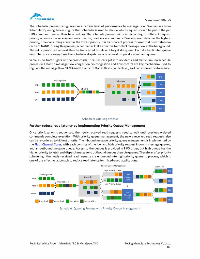
The scheduler process can guarantee a certain level of performance to message flow. We can see from Scheduler Queuing Process figure that scheduler is used to decide which request should be put in the per LUN command queue. How to schedule? The schedule process will start according to different request priority scheme after receive amounts of write, read, erase commands. Basically, read data has the highest priority, time-consuming erase has the lowest priority. It is transparent process for user that flush data from cache to NAND. During this process, scheduler will take effective to control message flow at the background. The set of prioritized request then be transferred to relevant target die queue. Each die has limited queue depth to process, every time the scheduler dispatches one request on per die command queue.
Same as no traffic lights on the crossroads, it causes cars get into accidents and traffic jam, no schedule process will lead to message flow congestion. So congestion and flow control are key mechanism used to regulate the message flow NAND inside to ensure QoS at flash channel level, so it can improve performance.
Scheduler Queuing Process
Further reduce read latency by implementing Priority Queue Management
Once prioritization is sequenced, the newly received read requests need to wait until previous ordered commands complete execution. With priority queue management, the newly received read requests also can be re-ordered to highest priority. The inbound message priority queue management is implemented by the Flash Channel Cores, with each consists of the low and high priority request inbound message queues, and an outbound message queue. Access to the queues is provided in FIFO order, but high queue has the higher priority to fetch and dispatch message to outbound queues then die queues. Therefore, after priority scheduling, the newly received read requests are enqueued into high priority queue to process, which is one of the effective approach to reduce read latency for mixed-used applications.
SchedulerWrite
Read
Erase
Die queue
Message flow
···
···
···
Mixed Stream
User Read
···
···
···
High Priority Queue
Low Priority Queue
Die
···
System Read User Write System Write
···
···
Die
···
Die
Die
···
Priority Queue Management
Flash Channel
Core
Flash Channel
Core
···
···
Scheduler Queuing Process with Priority Queue Management
Scheduler
Write
Read
Erase
Die queue
Message flow
···
···
···
Die
Die
Die
Die
Die
Mixed Stream
Memblaze® PBlaze5
Technical White Paper | MemSolid®3.0 & MemSpeed®3.0 Beijing Memblaze Technology Co., Ltd. 17
High Performance FTL
What is FTL?
There is a characteristic of SSD that in order to write to an area in the physical media, it must be erased on a block before. So writes to the same Logical Block Address (LBA) will be mapped to different physical locations on the flash media (PBA). The flash translation layer (FTL) is a hardware/software layer which is responsible for the logical to physical mapping of data. Apparently, the mapping efficiency of FTL influences the SSD performance directly.
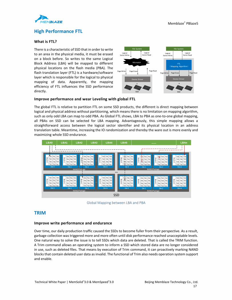
Improve performance and wear Leveling with global FTL
The global FTL is relative to partition FTL on some SSD products, the different is direct mapping between logical and physical address without partitioning, which means there is no limitation on mapping algorithm, such as only odd LBA can map to odd PBA. As Global FTL shows, LBA to PBA as one-to-one global mapping, all PBAs on SSD can be selected for LBA mapping. Advantageously, this simple mapping allows a straightforward access between the logical sector identifier and its physical location in an address translation table. Meantime, increasing the IO randomization and thereby the ware out is more evenly and maximizing whole SSD endurance.
SSD
Page
LBA0 LBA1 LBA2 LBA3 LBA4 LBA5 …… LBAn
Partition FTLGlobal FTL
NAND/Package NAND/Package
NAND/Package NAND/Package
...
PBA
Die 0
Blo
ck 0
Page Page Page
PagePage Page
Page Page Page
Page Page Page
Die 1B
lock 1
Page Page Page
PagePage Page
Page Page Page
Page Page Page
Die 2
Blo
ck 2
Page Page Page
PagePage Page
Page Page Page
Page Page Page
Die m
···
Die 0
Blo
ck 0
Page Page Page
PagePage Page
Page Page Page
Page Page Page
Die 1
Blo
ck 1
Page Page Page
PagePage Page
Page Page Page
Page Page Page
Die 2
Blo
ck 2
Page Page Page
PagePage Page
Page Page Page
Page Page Page
Die m
···
Blo
ck X
Page Page Page
PagePage Page
Page Page Page
Page Page Page
Blo
ck X
Page Page Page
PagePage Page
Page Page Page
Page Page Page
Die 0
Blo
ck 0
Page Page Page
PagePage Page
Page Page Page
Page Page Page
Die 1
Blo
ck 1
Page Page Page
PagePage Page
Page Page Page
Page Page Page
Die 2
Blo
ck 2
Page Page Page
PagePage Page
Page Page Page
Page Page Page
Die m
···
Blo
ck X
Page Page Page
PagePage Page
Page Page Page
Page Page Page
Die 0
Blo
ck 0
Page Page Page
PagePage Page
Page Page Page
Page Page Page
Die 1
Blo
ck 1
Page Page Page
PagePage Page
Page Page Page
Page Page Page
Die 2
Blo
ck 2
Page Page Page
PagePage Page
Page Page Page
Page Page Page
Die m
···
Blo
ck X
Page Page Page
PagePage Page
Page Page Page
Page Page Page
Global Mapping between LBA and PBA
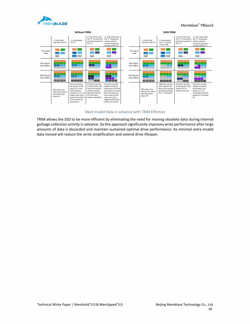
TRIM
Improve write performance and endurance
Over time, our daily production traffic caused the SSDs to become fuller from their perspective. As a result, garbage collection was triggered more and more often until disk performance reached unacceptable levels. One natural way to solve the issue is to tell SSDs which data are deleted. That is called the TRIM function. A Trim command allows an operating system to inform a SSD which stored data are no longer considered in use, such as deleted files. That means by execution of Trim command, it can proactively marking NAND blocks that contain deleted user data as invalid. The functional of Trim also needs operation system support and enable.
SSD
File System
Device Driver
LogicalSector Write
LogicalSector Read
Mismatch
Page Write
+
SSD
FTL
(Mapping Algorithm)
Device Driver
+
Page Erase Page Read
File System
LogicalSector Write
LogicalSector Read
Page Write Page Erase Page Read
Memblaze® PBlaze5
Technical White Paper | MemSolid®3.0 & MemSpeed®3.0 Beijing Memblaze Technology Co., Ltd. 18
OS Logical View
1. User writes new files A,B,C,D
2. User deletes file “C”
File A
File C
File B
Free
3. User writes new file “E” to overwrite previous location of File ”C”
SSD Logical View (LBAs)
A1 A2 A3 A4
B1 B2 B3 B4
C1 C2 D1 D2
A1 A2 A3 A4
B1 B2 B3 B4
C1 C2 D1 D2
File A
Free
File B
Free
SSD Physical View (PBAs)
File CX
A1 A2 A3 A4
B1 B2 B3 B4
E1 E2 D1 D2
SSD writes new data to free space, only SSD knows about OP
OS only removes the pointer to the data C1, C2 and only OS knows existed C1, C2 is no longer valid. SSD is aware of invalid C1, C2 once they are overwritten
OS writes new file to old location, SSD marks old location contains invalid data and ready for GC, file E gets written elsewhere
File A File B
Free
File EFile D
A1 A2 A3 A4
B1 B2 B3 B4
C1 C2 D1 D2
Over Provisioning
A1 A2 A3 A4
B1 B2 B3 B4
C1 C2 D1 D2
A1 A2 A3 A4
B1 B2 B3 B4
GC GC D1 D2
E1 E2
File D File D
A1 A2 A3 A4
B1 B2 B3 B4
C1 F1 D1 D2
F2 F3
3’. User writes new file “F” and partial written without overwrite previous location of File ”C”
File A File B
Free
File FFile D
A1 A2 A3 A4
B1 B2 B3 B4
GC GC D1 D2
F1 F2 F3
C1
OS writes new file without overwrite old location, SSD will still treat C1 as valid data and may have extra move to free space once GC is triggered, file F gets written elsewhere
Without TRIM
OS Logical View
1. User writes new files A,B,C,D
2. User deletes file “C” and OS sends TRIM
File A
File C
File B
Free
3. User writes new file “E” to overwrite previous location of File ”C”
SSD Logical View (LBAs)
File A
Free
File B
Free
SSD Physical View (PBAs)
File CX
SSD writes new data to free space, only SSD knows about OP
TRIM from OS tells SSD to ignore the data in the location previously holding file “C” during GC
OS writes new file to old location, SSD writes file E to another free area
File A File B
Free
File EFile D
Over Provisioning
File D File D
3’. User writes new file “F” and partial written without overwrite previous location of File ”C”
File A File B
Free
File FFile D
OS writes new file without overwrite old location, SSD knows C1, C2 is invalid data and will ignore C1, C2 during GC
With TRIM
A1 A2 A3 A4
B1 B2 B3 B4
C1 C2 D1 D2
A1 A2 A3 A4
B1 B2 B3 B4
D1 D2
A1 A2 A3 A4
B1 B2 B3 B4
E1 E2 D1 D2
A1 A2 A3 A4
B1 B2 B3 B4
C1 C2 D1 D2
Over Provisioning
A1 A2 A3 A4
B1 B2 B3 B4
GC GC D1 D2
A1 A2 A3 A4
B1 B2 B3 B4
GC GC D1 D2
E1 E2
A1 A2 A3 A4
B1 B2 B3 B4
F1 D1 D2
F2 F3
A1 A2 A3 A4
B1 B2 B3 B4
GC GC D1 D2
F1 F2 F3
Mark Invalid Data in advance with TRIM Effective
TRIM allows the SSD to be more efficient by eliminating the need for moving obsolete data during internal garbage collection activity in advance. So this approach significantly improves write performance after large amounts of data is discarded and maintain sustained optimal drive performance. As minimal extra invalid data moved will reduce the write amplification and extend drive lifespan.
Memblaze® PBlaze5
Technical White Paper | MemSolid®3.0 & MemSpeed®3.0 Beijing Memblaze Technology Co., Ltd. 19
Proven Data Reliability with MemSolid®3.0
There is no doubt that companies in every industry sector around the world have seen their sensitive data
corrupted or lost, and there are so many reason why data integrity problems can occur, such as the
operation system bugs, storage hardware and firmware bugs, “the human factors” that administrative
errors are also a major risk. In addition, as technology evolved rapidly, multi core processes is increasing
(Intel 18-core Haswell Xeon processer is applied widely), memory is expanding, wire speeds is doubling
(100Gb InfiniBand has out the door for high performance applications such as clustered storage arrays),
those technology transitions also can add data corruption risk. Data corruption risk is everywhere, even
from the cosmic rays created by exploding stars.
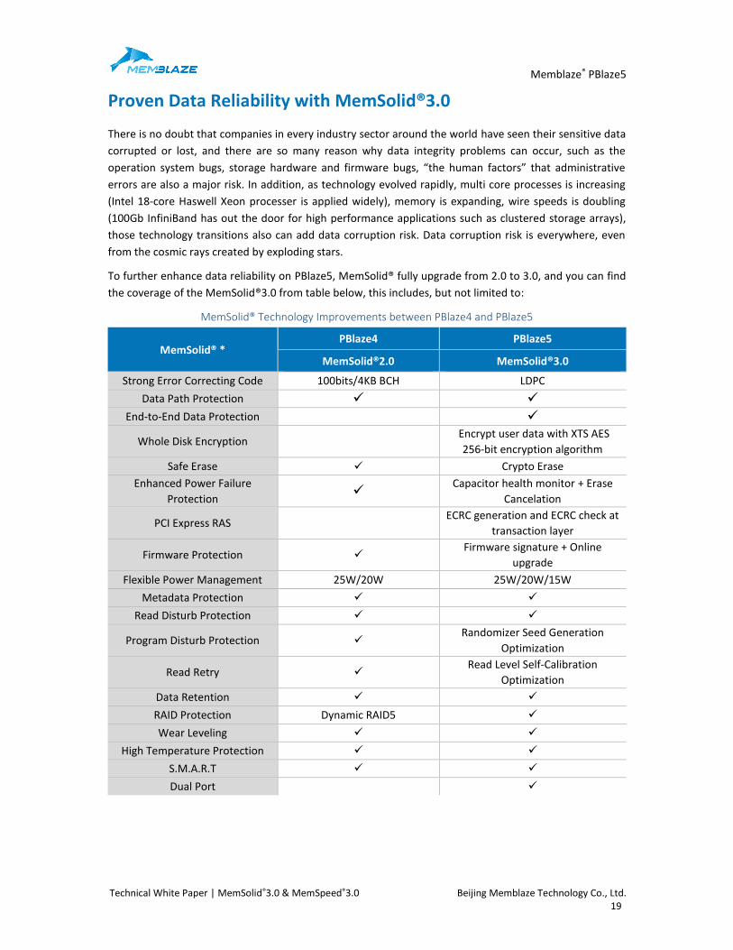
To further enhance data reliability on PBlaze5, MemSolid® fully upgrade from 2.0 to 3.0, and you can find
the coverage of the MemSolid®3.0 from table below, this includes, but not limited to:
MemSolid® Technology Improvements between PBlaze4 and PBlaze5
MemSolid® * PBlaze4 PBlaze5
MemSolid®2.0 MemSolid®3.0
Strong Error Correcting Code 100bits/4KB BCH LDPC
Data Path Protection ✓ ✓
End-to-End Data Protection ✓
Whole Disk Encryption Encrypt user data with XTS AES
256-bit encryption algorithm
Safe Erase ✓ Crypto Erase
Enhanced Power Failure
Protection ✓
Capacitor health monitor + Erase
Cancelation
PCI Express RAS ECRC generation and ECRC check at
transaction layer
Firmware Protection ✓ Firmware signature + Online
upgrade
Flexible Power Management 25W/20W 25W/20W/15W
Metadata Protection ✓ ✓
Read Disturb Protection ✓ ✓
Program Disturb Protection ✓ Randomizer Seed Generation
Optimization
Read Retry ✓ Read Level Self-Calibration
Optimization
Data Retention ✓ ✓
RAID Protection Dynamic RAID5 ✓
Wear Leveling ✓ ✓
High Temperature Protection ✓ ✓
S.M.A.R.T ✓ ✓
Dual Port ✓
Memblaze® PBlaze5
Technical White Paper | MemSolid®3.0 & MemSpeed®3.0 Beijing Memblaze Technology Co., Ltd. 20
Strong Error Correcting Code - LDPC
Why LDPC?
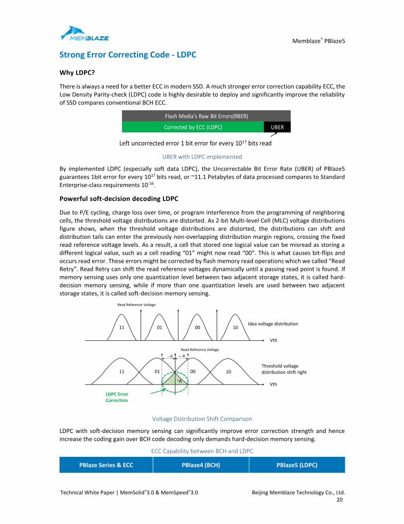
There is always a need for a better ECC in modern SSD. A much stronger error correction capability ECC, the Low Density Parity-check (LDPC) code is highly desirable to deploy and significantly improve the reliability of SSD compares conventional BCH ECC.
Corrected by ECC (LDPC)
Flash Media’s Raw Bit Errors(RBER)
UBER
Left uncorrected error 1 bit error for every 1017 bits read
UBER with LDPC implemented
By implemented LDPC (especially soft data LDPC), the Uncorrectable Bit Error Rate (UBER) of PBlaze5 guarantees 1bit error for every 1017 bits read, or ~11.1 Petabytes of data processed compares to Standard Enterprise-class requirements 10-16.
Powerful soft-decision decoding LDPC
Due to P/E cycling, charge loss over time, or program interference from the programming of neighboring cells, the threshold voltage distributions are distorted. As 2-bit Multi-level Cell (MLC) voltage distributions figure shows, when the threshold voltage distributions are distorted, the distributions can shift and distribution tails can enter the previously non-overlapping distribution margin regions, crossing the fixed read reference voltage levels. As a result, a cell that stored one logical value can be misread as storing a different logical value, such as a cell reading “01” might now read “00”. This is what causes bit-flips and occurs read error. These errors might be corrected by flash memory read operations which we called “Read Retry”. Read Retry can shift the read reference voltages dynamically until a passing read point is found. If memory sensing uses only one quantization level between two adjacent storage states, it is called hard-decision memory sensing, while if more than one quantization levels are used between two adjacent storage states, it is called soft-decision memory sensing.
Voltage Distribution Shift Comparison
LDPC with soft-decision memory sensing can significantly improve error correction strength and hence increase the coding gain over BCH code decoding only demands hard-decision memory sensing.
ECC Capability between BCH and LDPC
PBlaze Series & ECC PBlaze4 (BCH) PBlaze5 (LDPC)
11 01 00 10
Vth
Read Reference Voltage
-△B +△B
Idea voltage distribution
Threshold voltage distribution shift right
·A
11 01 00 10
Vth
Read Reference Voltage
LDPC Error Correction
Memblaze® PBlaze5
Technical White Paper | MemSolid®3.0 & MemSpeed®3.0 Beijing Memblaze Technology Co., Ltd. 21
ECC Capability 100bit / 4KB 550bit / 4KB
LDPC in NAND
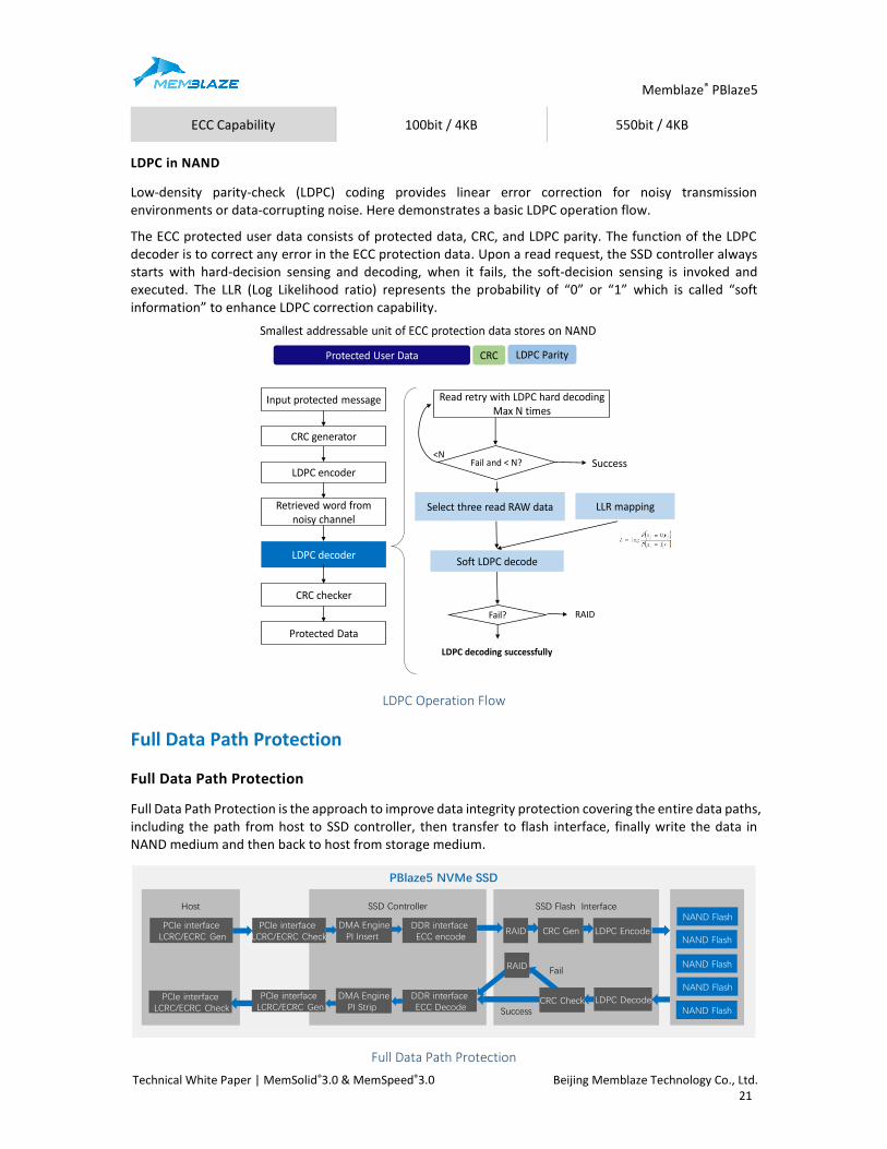
Low-density parity-check (LDPC) coding provides linear error correction for noisy transmission environments or data-corrupting noise. Here demonstrates a basic LDPC operation flow.
The ECC protected user data consists of protected data, CRC, and LDPC parity. The function of the LDPC decoder is to correct any error in the ECC protection data. Upon a read request, the SSD controller always starts with hard-decision sensing and decoding, when it fails, the soft-decision sensing is invoked and executed. The LLR (Log Likelihood ratio) represents the probability of “0” or “1” which is called “soft information” to enhance LDPC correction capability.
Input protected message
LDPC encoder
Retrieved word from noisy channel
LDPC decoder
Read retry with LDPC hard decodingMax N times
Select three read RAW data
Fail?
Fail and < N?
LDPC decoding successfully
RAID
Success
LLR mapping
CRC generator
CRC checker
Protected User Data CRC LDPC Parity
Smallest addressable unit of ECC protection data stores on NAND
Soft LDPC decode
Protected Data
<N
LDPC Operation Flow
Full Data Path Protection
Full Data Path Protection
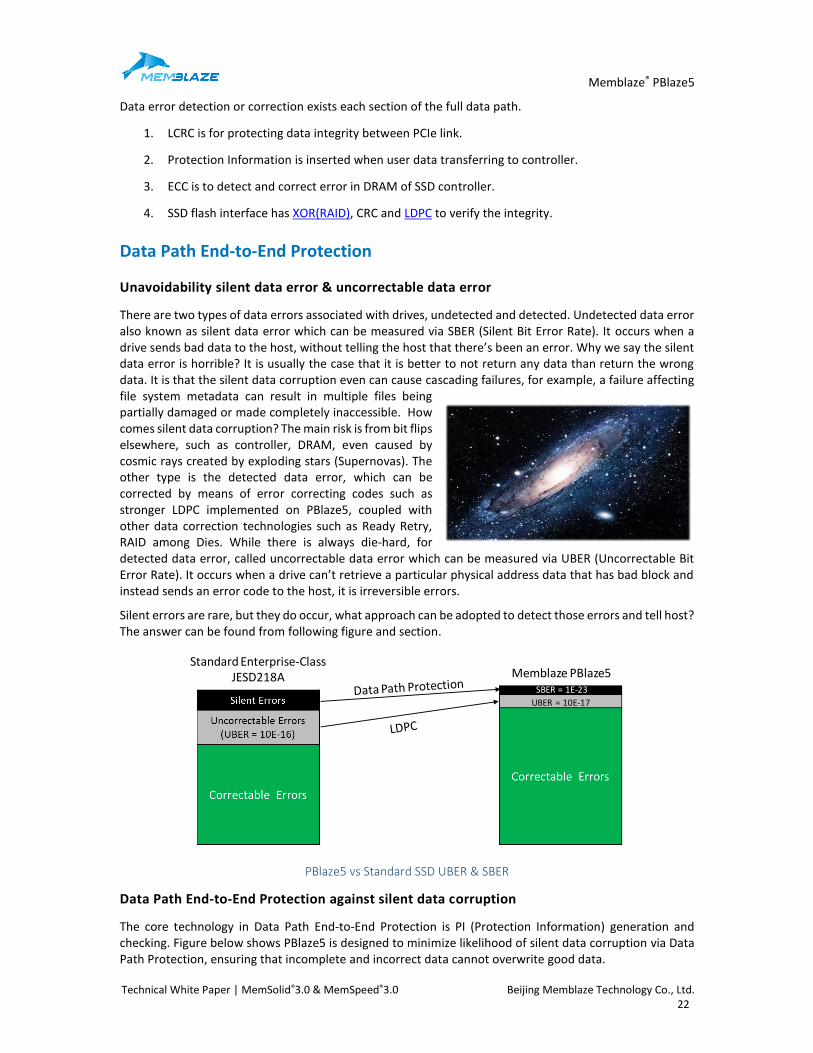
Full Data Path Protection is the approach to improve data integrity protection covering the entire data paths, including the path from host to SSD controller, then transfer to flash interface, finally write the data in NAND medium and then back to host from storage medium.
PBlaze5 NVMe SSD
Host SSD Controller SSD Flash Interface
PCIe interfaceLCRC/ECRC Gen
PCIe interfaceLCRC/ECRC Check
PCIe interfaceLCRC/ECRC Gen
PCIe interface LCRC/ECRC Check
DDR interfaceECC encode
DDR interfaceECC Decode
RAID CRC Gen LDPC Encode
LDPC Decode
RAID
CRC Check
Fail
Success
NAND Flash
NAND Flash
NAND Flash
NAND Flash
NAND Flash
DMA EnginePI Insert
DMA EnginePI Strip
Full Data Path Protection
Memblaze® PBlaze5
Technical White Paper | MemSolid®3.0 & MemSpeed®3.0 Beijing Memblaze Technology Co., Ltd. 22
Data error detection or correction exists each section of the full data path.
1. LCRC is for protecting data integrity between PCIe link.
2. Protection Information is inserted when user data transferring to controller.
3. ECC is to detect and correct error in DRAM of SSD controller.
4. SSD flash interface has XOR(RAID), CRC and LDPC to verify the integrity.
Data Path End-to-End Protection
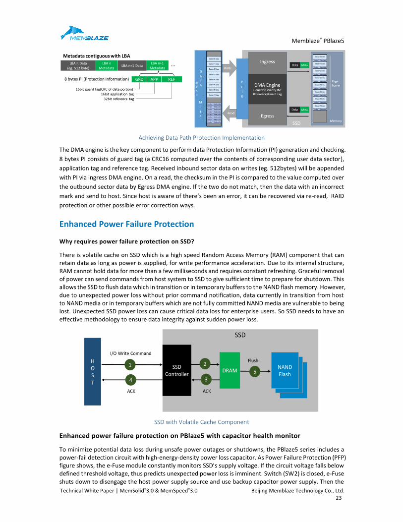
Unavoidability silent data error & uncorrectable data error
There are two types of data errors associated with drives, undetected and detected. Undetected data error also known as silent data error which can be measured via SBER (Silent Bit Error Rate). It occurs when a drive sends bad data to the host, without telling the host that there’s been an error. Why we say the silent data error is horrible? It is usually the case that it is better to not return any data than return the wrong data. It is that the silent data corruption even can cause cascading failures, for example, a failure affecting file system metadata can result in multiple files being partially damaged or made completely inaccessible. How comes silent data corruption? The main risk is from bit flips elsewhere, such as controller, DRAM, even caused by cosmic rays created by exploding stars (Supernovas). The other type is the detected data error, which can be corrected by means of error correcting codes such as stronger LDPC implemented on PBlaze5, coupled with other data correction technologies such as Ready Retry, RAID among Dies. While there is always die-hard, for detected data error, called uncorrectable data error which can be measured via UBER (Uncorrectable Bit Error Rate). It occurs when a drive can’t retrieve a particular physical address data that has bad block and instead sends an error code to the host, it is irreversible errors.
Silent errors are rare, but they do occur, what approach can be adopted to detect those errors and tell host? The answer can be found from following figure and section.
Standard Enterprise-ClassJESD218A Memblaze PBlaze5
SBER = 1E-23
UBER = 10E-17
PBlaze5 vs Standard SSD UBER & SBER
Data Path End-to-End Protection against silent data corruption
The core technology in Data Path End-to-End Protection is PI (Protection Information) generation and checking. Figure below shows PBlaze5 is designed to minimize likelihood of silent data corruption via Data Path Protection, ensuring that incomplete and incorrect data cannot overwrite good data.
Memblaze® PBlaze5
Technical White Paper | MemSolid®3.0 & MemSpeed®3.0 Beijing Memblaze Technology Co., Ltd. 23
SSD
Data
LBA n Data(eg. 512 byte)
LBA nMetadata
GRD APP REF8 bytes PI (Protection Information)
16bit guard tag(CRC of data portion)16bit application tag
32bit reference tag
LBA n+1 DataLBA n+1
Metadata
Metadata contiguous with LBA
···
PI
Data
Data
DMA engineData
Processing UnitPIData
Insert PI via Ingress DMA engine
Check PI via Egress DMA engine
Ho
st
PC
Ie
Ingress
Egress
Achieving Data Path Protection Implementation
The DMA engine is the key component to perform data Protection Information (PI) generation and checking.
8 bytes PI consists of guard tag (a CRC16 computed over the contents of corresponding user data sector),
application tag and reference tag. Received inbound sector data on writes (eg. 512bytes) will be appended
with PI via ingress DMA engine. On a read, the checksum in the PI is compared to the value computed over
the outbound sector data by Egress DMA engine. If the two do not match, then the data with an incorrect
mark and send to host. Since host is aware of there‘s been an error, it can be recovered via re-read, RAID
protection or other possible error correction ways.
Enhanced Power Failure Protection
Why requires power failure protection on SSD?
There is volatile cache on SSD which is a high speed Random Access Memory (RAM) component that can retain data as long as power is supplied, for write performance acceleration. Due to its internal structure, RAM cannot hold data for more than a few milliseconds and requires constant refreshing. Graceful removal of power can send commands from host system to SSD to give sufficient time to prepare for shutdown. This allows the SSD to flush data which in transition or in temporary buffers to the NAND flash memory. However, due to unexpected power loss without prior command notification, data currently in transition from host to NAND media or in temporary buffers which are not fully committed NAND media are vulnerable to being lost. Unexpected SSD power loss can cause critical data loss for enterprise users. So SSD needs to have an effective methodology to ensure data integrity against sudden power loss.
SSD
NAND Flash
NAND Flash
NAND Flash
DRAM1
4
I/O Write Command
ACK
5
FlushHOST
SSD Controller
2
3
ACK
SSD with Volatile Cache Component
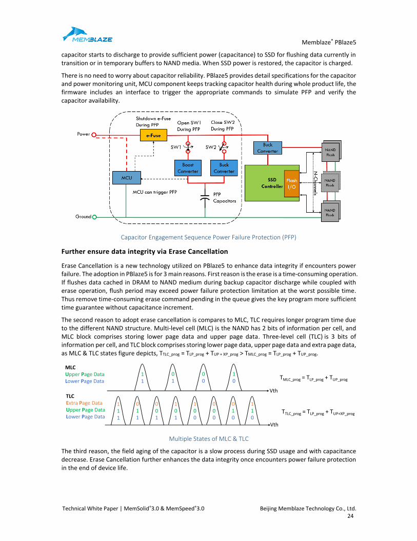
Enhanced power failure protection on PBlaze5 with capacitor health monitor
To minimize potential data loss during unsafe power outages or shutdowns, the PBlaze5 series includes a power-fail detection circuit with high-energy-density power loss capacitor. As Power Failure Protection (PFP) figure shows, the e-Fuse module constantly monitors SSD’s supply voltage. If the circuit voltage falls below defined threshold voltage, thus predicts unexpected power loss is imminent. Switch (SW2) is closed, e-Fuse shuts down to disengage the host power supply source and use backup capacitor power supply. Then the
Memblaze® PBlaze5
Technical White Paper | MemSolid®3.0 & MemSpeed®3.0 Beijing Memblaze Technology Co., Ltd. 24
capacitor starts to discharge to provide sufficient power (capacitance) to SSD for flushing data currently in transition or in temporary buffers to NAND media. When SSD power is restored, the capacitor is charged.
There is no need to worry about capacitor reliability. PBlaze5 provides detail specifications for the capacitor and power monitoring unit, MCU component keeps tracking capacitor health during whole product life, the firmware includes an interface to trigger the appropriate commands to simulate PFP and verify the capacitor availability.
Capacitor Engagement Sequence Power Failure Protection (PFP)
Further ensure data integrity via Erase Cancellation
Erase Cancellation is a new technology utilized on PBlaze5 to enhance data integrity if encounters power failure. The adoption in PBlaze5 is for 3 main reasons. First reason is the erase is a time-consuming operation. If flushes data cached in DRAM to NAND medium during backup capacitor discharge while coupled with erase operation, flush period may exceed power failure protection limitation at the worst possible time. Thus remove time-consuming erase command pending in the queue gives the key program more sufficient time guarantee without capacitance increment.
The second reason to adopt erase cancellation is compares to MLC, TLC requires longer program time due to the different NAND structure. Multi-level cell (MLC) is the NAND has 2 bits of information per cell, and MLC block comprises storing lower page data and upper page data. Three-level cell (TLC) is 3 bits of information per cell, and TLC block comprises storing lower page data, upper page data and extra page data, as MLC & TLC states figure depicts, TTLC_prog = TLP_prog + TUP + XP_prog > TMLC_prog = TLP_prog + TUP_prog.
111
011
001
101
100
000
010
110
Vth
TLCExtra Page Data Upper Page DataLower Page Data
11
01
00
10
Vth
MLCUpper Page DataLower Page Data
TTLC_prog = TLP_prog + TUP+XP_prog
TMLC_prog = TLP_prog + TUP_prog
Multiple States of MLC & TLC
The third reason, the field aging of the capacitor is a slow process during SSD usage and with capacitance decrease. Erase Cancellation further enhances the data integrity once encounters power failure protection in the end of device life.
Memblaze® PBlaze5
Technical White Paper | MemSolid®3.0 & MemSpeed®3.0 Beijing Memblaze Technology Co., Ltd. 25
PCI Express ECRC Protection
Understanding PCIe Link
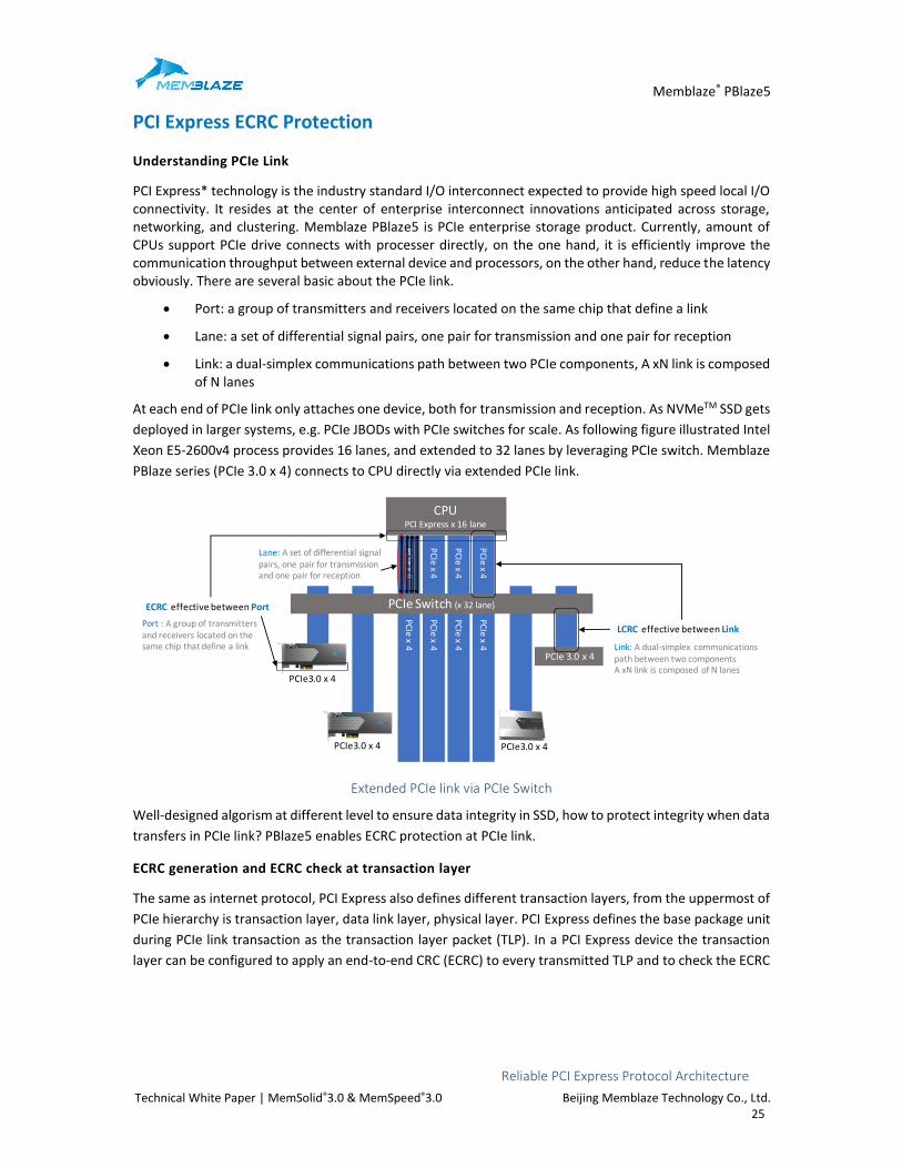
PCI Express* technology is the industry standard I/O interconnect expected to provide high speed local I/O connectivity. It resides at the center of enterprise interconnect innovations anticipated across storage, networking, and clustering. Memblaze PBlaze5 is PCIe enterprise storage product. Currently, amount of CPUs support PCIe drive connects with processer directly, on the one hand, it is efficiently improve the communication throughput between external device and processors, on the other hand, reduce the latency obviously. There are several basic about the PCIe link.
• Port: a group of transmitters and receivers located on the same chip that define a link
• Lane: a set of differential signal pairs, one pair for transmission and one pair for reception
• Link: a dual-simplex communications path between two PCIe components, A xN link is composed of N lanes
At each end of PCIe link only attaches one device, both for transmission and reception. As NVMeTM SSD gets
deployed in larger systems, e.g. PCIe JBODs with PCIe switches for scale. As following figure illustrated Intel
Xeon E5-2600v4 process provides 16 lanes, and extended to 32 lanes by leveraging PCIe switch. Memblaze
PBlaze series (PCIe 3.0 x 4) connects to CPU directly via extended PCIe link.
CPUPCI Express x 16 lane
PC
Iex 4
PC
Iex 4
PC
Iex 4
PC
Iex 4
PC
Iex 4
PC
Iex 4
PC
Iex 4
PC
Iex 4
PCIe Switch (x 32 lane)
PCIe 3.0 x 4
PCIe3.0 x 4
PCIe3.0 x 4
PCIe3.0 x 4
ECRC effective between Port
Port : A group of transmitters and receivers located on the same chip that define a link
LCRC effective between Link
Link: A dual-simplex communications path between two componentsA xN link is composed of N lanes
Lane: A set of differential signal pairs, one pair for transmission and one pair for reception
Extended PCIe link via PCIe Switch
Well-designed algorism at different level to ensure data integrity in SSD, how to protect integrity when data
transfers in PCIe link? PBlaze5 enables ECRC protection at PCIe link.
ECRC generation and ECRC check at transaction layer
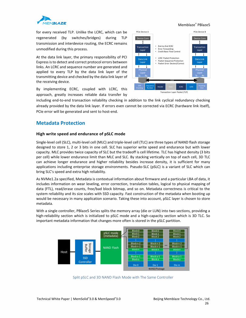
The same as internet protocol, PCI Express also defines different transaction layers, from the uppermost of
PCIe hierarchy is transaction layer, data link layer, physical layer. PCI Express defines the base package unit
during PCIe link transaction as the transaction layer packet (TLP). In a PCI Express device the transaction
layer can be configured to apply an end-to-end CRC (ECRC) to every transmitted TLP and to check the ECRC
Reliable PCI Express Protocol Architecture
Memblaze® PBlaze5
Technical White Paper | MemSolid®3.0 & MemSpeed®3.0 Beijing Memblaze Technology Co., Ltd. 26
for every received TLP. Unlike the LCRC, which can be
regenerated (by switches/bridges) during TLP
transmission and interdevice routing, the ECRC remains
unmodified during this process.
At the data link layer, the primary responsibility of PCI Express is to detect and correct protocol errors between links. An LCRC and sequence number are generated and applied to every TLP by the data link layer of the transmitting device and checked by the data link layer of the receiving device.
By implementing ECRC, coupled with LCRC, this
approach, greatly increases reliable data transfer by
including end-to-end transaction reliability checking in addition to the link cyclical redundancy checking
already provided by the data link layer. If errors even cannot be corrected via ECRC (hardware link itself),
PCIe error will be generated and sent to host-end.
Metadata Protection
High write speed and endurance of pSLC mode
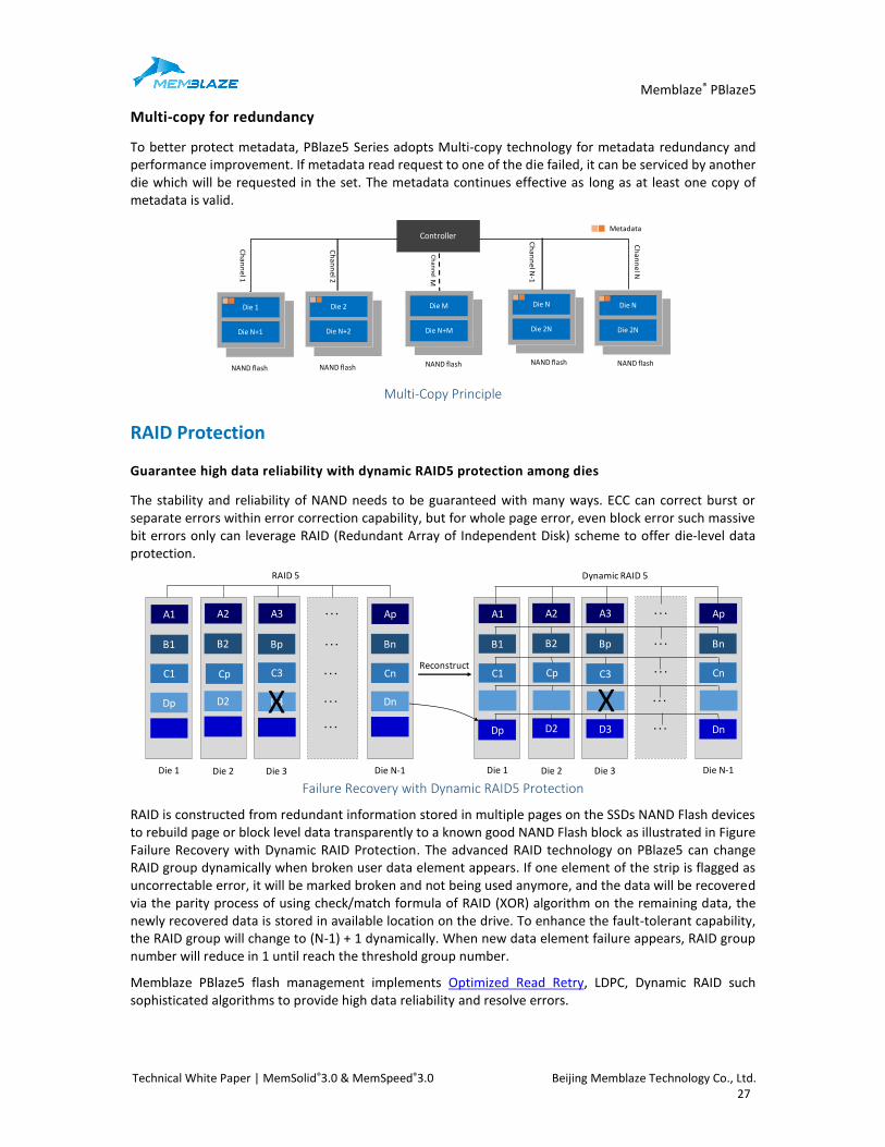
Single-level cell (SLC), multi-level cell (MLC) and triple-level cell (TLC) are three types of NAND flash storage designed to store 1, 2 or 3 bits in one cell. SLC has superior write speed and endurance but with lower capacity. MLC provides twice capacity of SLC but the tradeoff is cell lifetime. TLC has highest density (3 bits per cell) while lower endurance limit than MLC and SLC. By stacking vertically on top of each cell, 3D TLC can achieve longer endurance and higher reliability besides increase density, it is sufficient for many applications including enterprise storage environments. Pseudo-SLC (pSLC) is a variant of SLC which can bring SLC’s speed and extra high reliability.
As NVMe1.2a specified, Metadata is contextual information about firmware and a particular LBA of data, it includes information on wear leveling, error correction, translation tables, logical to physical mapping of data (FTL), read/erase counts, free/bad block bitmap, and so on. Metadata correctness is critical to the system reliability and its size scales with SSD capacity. Fast construction of the metadata when booting up would be necessary in many application scenario. Taking these into account, pSLC layer is chosen to store metadata.
With a single controller, PBlaze5 Series splits the memory array (die or LUN) into two sections, providing a high-reliability section which is initialized to pSLC mode and a high-capacity section which is 3D TLC. So important metadata information that changes more often is stored in the pSLC partition.
Host
SSD Controller
Storage
Bu
ffer
NAND Flash
pSLC mode(metadata)
NAND/Package
Die 0
...
Block 0Block 1
Block n
Block a
...
Block 2
...
Block n-2
Block a-1
Block n-1
Die 1
...
Block 0Block 1
Block n
Block a
Block 2
...
Block n-2
Block a-1
Block n-1
Die m
...
Block 0Block 1
Block n
Block a
Block 2
...
Block n-2
Block a-1
Block n-1
Split pSLC and 3D NAND Flash Mode with The Same Controller
Transaction Layer
Data Link Layer
Physical Layer
Tx Rx
Device Core
Transaction Layer
Data Link Layer
Physical Layer
Tx Rx
Device Core
ECRC LCRCFraming
EndDataHeader
Sequence Number
STP Framing
Link
PCIe Device B
• End-to-End ECRC
• Error Forwarding• Credit Base Flow Control
• LCRC Packet Protection
• Packet Sequence Protection• Packet Error Dectect/Correct
PCIe Device A
Transaction Layer Packet (TLP)
Memblaze® PBlaze5
Technical White Paper | MemSolid®3.0 & MemSpeed®3.0 Beijing Memblaze Technology Co., Ltd. 27
Multi-copy for redundancy
To better protect metadata, PBlaze5 Series adopts Multi-copy technology for metadata redundancy and performance improvement. If metadata read request to one of the die failed, it can be serviced by another die which will be requested in the set. The metadata continues effective as long as at least one copy of metadata is valid.
Die 1(metadata 1)
Die 2
Die 3
Die 4
Die 1(metadata 1)
Die 2
Die 1
Die N+1
Die M
Die N+M
Die N
Die 2N
Controller
NAND flash NAND flash NAND flash
Die 1(metadata 1)
Die 2
Die 2
Die N+2
NAND flash
Ch
an
ne
l 1
Ch
an
ne
l 2
Ch
an
ne
l N
Ch
ann
elM
Metadata
Die 1(metadata 1)
Die 2
Die N
Die 2N
NAND flashC
ha
nn
el N
-1
Multi-Copy Principle
RAID Protection
Guarantee high data reliability with dynamic RAID5 protection among dies
The stability and reliability of NAND needs to be guaranteed with many ways. ECC can correct burst or separate errors within error correction capability, but for whole page error, even block error such massive bit errors only can leverage RAID (Redundant Array of Independent Disk) scheme to offer die-level data protection.
A1 A2 Ap· · ·A3
B1 B2 Bn
C1 CnC3
D3D2 DnDp
Die 1 Die 2 Die 3 Die N-1
Bp
Cp
A1 A2 ApA3
B1 B2 Bn
C1 CnC3
D3D2 DnDp
Die 1 Die 2 Die 3 Die N-1
Bp· · ·
· · ·
· · ·
· · ·
· · ·
· · ·
· · ·
Reconstruct
X
RAID 5 Dynamic RAID 5
· · ·
· · ·
Cp
X
Failure Recovery with Dynamic RAID5 Protection
RAID is constructed from redundant information stored in multiple pages on the SSDs NAND Flash devices to rebuild page or block level data transparently to a known good NAND Flash block as illustrated in Figure Failure Recovery with Dynamic RAID Protection. The advanced RAID technology on PBlaze5 can change RAID group dynamically when broken user data element appears. If one element of the strip is flagged as uncorrectable error, it will be marked broken and not being used anymore, and the data will be recovered via the parity process of using check/match formula of RAID (XOR) algorithm on the remaining data, the newly recovered data is stored in available location on the drive. To enhance the fault-tolerant capability, the RAID group will change to (N-1) + 1 dynamically. When new data element failure appears, RAID group number will reduce in 1 until reach the threshold group number.
Memblaze PBlaze5 flash management implements Optimized Read Retry, LDPC, Dynamic RAID such sophisticated algorithms to provide high data reliability and resolve errors.
Memblaze® PBlaze5
Technical White Paper | MemSolid®3.0 & MemSpeed®3.0 Beijing Memblaze Technology Co., Ltd. 28
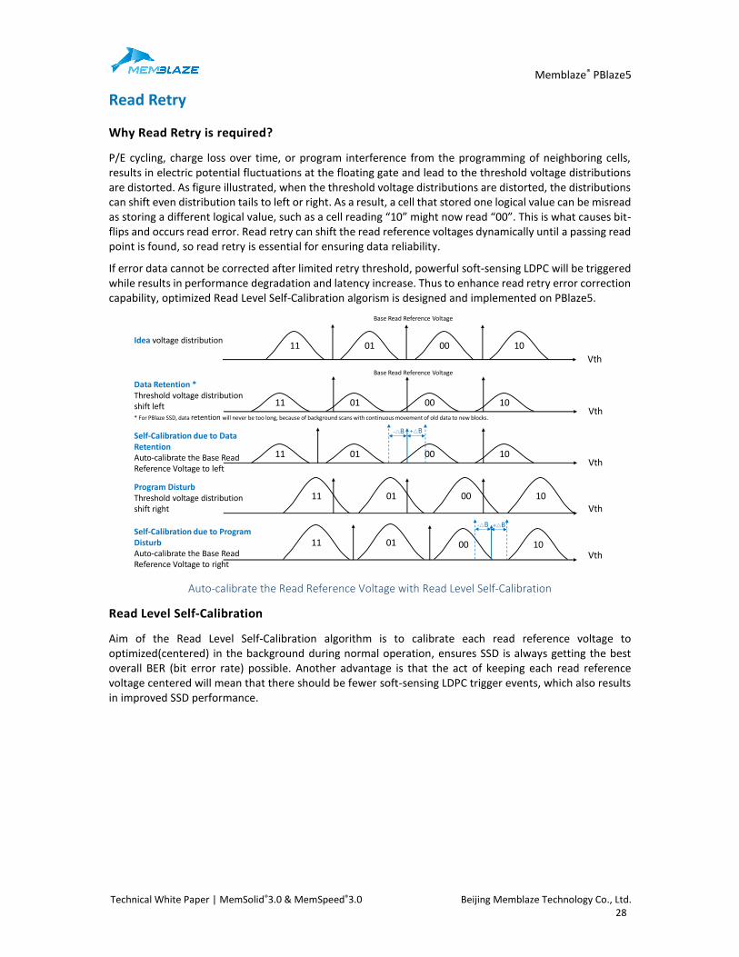
Read Retry
Why Read Retry is required?
P/E cycling, charge loss over time, or program interference from the programming of neighboring cells, results in electric potential fluctuations at the floating gate and lead to the threshold voltage distributions are distorted. As figure illustrated, when the threshold voltage distributions are distorted, the distributions can shift even distribution tails to left or right. As a result, a cell that stored one logical value can be misread as storing a different logical value, such as a cell reading “10” might now read “00”. This is what causes bit-flips and occurs read error. Read retry can shift the read reference voltages dynamically until a passing read point is found, so read retry is essential for ensuring data reliability.
If error data cannot be corrected after limited retry threshold, powerful soft-sensing LDPC will be triggered while results in performance degradation and latency increase. Thus to enhance read retry error correction capability, optimized Read Level Self-Calibration algorism is designed and implemented on PBlaze5.
11 01 00 10
Vth
Idea voltage distribution
Base Read Reference Voltage
Data Retention *Threshold voltage distribution shift left 11 01 00 10
Vth
Base Read Reference Voltage
Program DisturbThreshold voltage distribution shift right
11 01 00 10Vth
Self-Calibration due to Data RetentionAuto-calibrate the Base Read Reference Voltage to left
11 01 00 10Vth
-△B +△B
11 01 00 10Vth
Self-Calibration due to Program DisturbAuto-calibrate the Base Read Reference Voltage to right
-△B +△B
* For PBlaze SSD, data retention will never be too long, because of background scans with continuous movement of old data to new blocks.
Auto-calibrate the Read Reference Voltage with Read Level Self-Calibration
Read Level Self-Calibration
Aim of the Read Level Self-Calibration algorithm is to calibrate each read reference voltage to optimized(centered) in the background during normal operation, ensures SSD is always getting the best overall BER (bit error rate) possible. Another advantage is that the act of keeping each read reference voltage centered will mean that there should be fewer soft-sensing LDPC trigger events, which also results in improved SSD performance.
Memblaze® PBlaze5
Technical White Paper | MemSolid®3.0 & MemSpeed®3.0 Beijing Memblaze Technology Co., Ltd. 29
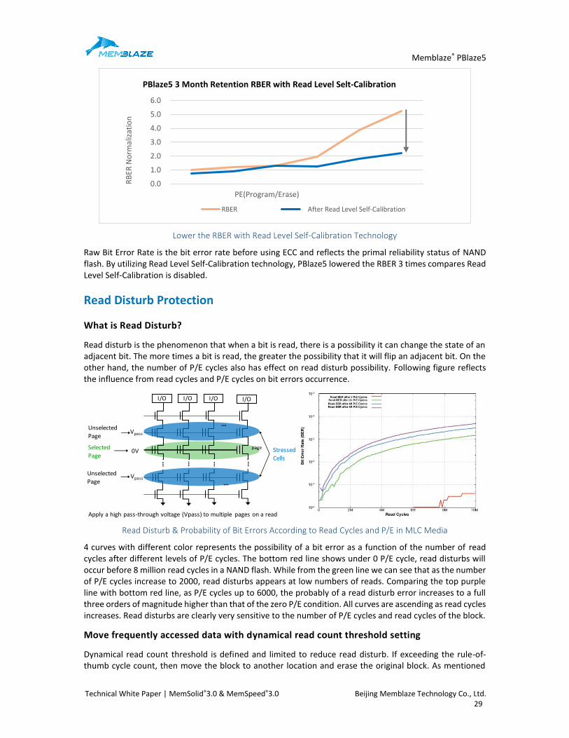
Lower the RBER with Read Level Self-Calibration Technology
Raw Bit Error Rate is the bit error rate before using ECC and reflects the primal reliability status of NAND flash. By utilizing Read Level Self-Calibration technology, PBlaze5 lowered the RBER 3 times compares Read Level Self-Calibration is disabled.
Read Disturb Protection
What is Read Disturb?
Read disturb is the phenomenon that when a bit is read, there is a possibility it can change the state of an adjacent bit. The more times a bit is read, the greater the possibility that it will flip an adjacent bit. On the other hand, the number of P/E cycles also has effect on read disturb possibility. Following figure reflects the influence from read cycles and P/E cycles on bit errors occurrence.
Selected
PageStressed
Cells0V
I/O I/O I/O I/O
Unselected
Page
Unselected
Page
···
···
···
···
···
···
Apply a high pass-through voltage (Vpass) to multiple pages on a read
Vpass
Vpass
page
Read Disturb & Probability of Bit Errors According to Read Cycles and P/E in MLC Media
4 curves with different color represents the possibility of a bit error as a function of the number of read cycles after different levels of P/E cycles. The bottom red line shows under 0 P/E cycle, read disturbs will occur before 8 million read cycles in a NAND flash. While from the green line we can see that as the number of P/E cycles increase to 2000, read disturbs appears at low numbers of reads. Comparing the top purple line with bottom red line, as P/E cycles up to 6000, the probably of a read disturb error increases to a full three orders of magnitude higher than that of the zero P/E condition. All curves are ascending as read cycles increases. Read disturbs are clearly very sensitive to the number of P/E cycles and read cycles of the block.
Move frequently accessed data with dynamical read count threshold setting
Dynamical read count threshold is defined and limited to reduce read disturb. If exceeding the rule-of-thumb cycle count, then move the block to another location and erase the original block. As mentioned
0.0
1.0
2.0
3.0
4.0
5.0
6.0
RB
ER N
orm
aliz
atio
n
PE(Program/Erase)
PBlaze5 3 Month Retention RBER with Read Level Selt-Calibration
RBER After cRLC RBERAfter Read Level Self-Calibration
Memblaze® PBlaze5
Technical White Paper | MemSolid®3.0 & MemSpeed®3.0 Beijing Memblaze Technology Co., Ltd. 30
above, strong LDPC ECC is utilized to correct this error once appears. By leveraging read disturb protection algorithm, PBlaze5 can greatly prevent and reduce the possibility of a read disturb event.
Program Disturb Protection
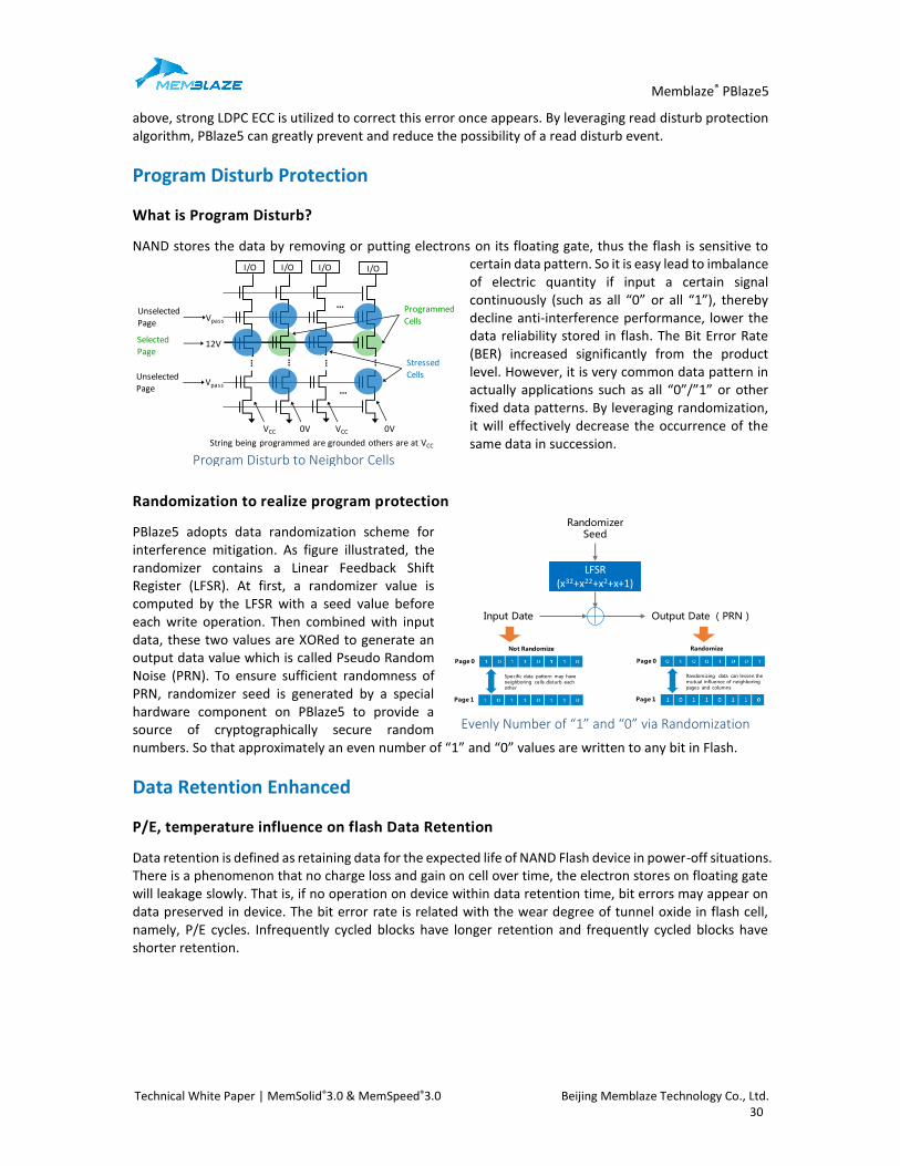
What is Program Disturb?
NAND stores the data by removing or putting electrons on its floating gate, thus the flash is sensitive to certain data pattern. So it is easy lead to imbalance of electric quantity if input a certain signal continuously (such as all “0” or all “1”), thereby decline anti-interference performance, lower the data reliability stored in flash. The Bit Error Rate (BER) increased significantly from the product level. However, it is very common data pattern in actually applications such as all “0”/”1” or other fixed data patterns. By leveraging randomization, it will effectively decrease the occurrence of the same data in succession.
Randomization to realize program protection
PBlaze5 adopts data randomization scheme for interference mitigation. As figure illustrated, the randomizer contains a Linear Feedback Shift Register (LFSR). At first, a randomizer value is computed by the LFSR with a seed value before each write operation. Then combined with input data, these two values are XORed to generate an output data value which is called Pseudo Random Noise (PRN). To ensure sufficient randomness of PRN, randomizer seed is generated by a special hardware component on PBlaze5 to provide a source of cryptographically secure random numbers. So that approximately an even number of “1” and “0” values are written to any bit in Flash.
Data Retention Enhanced
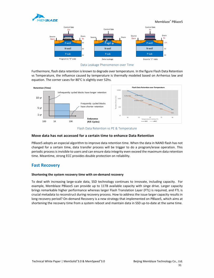
P/E, temperature influence on flash Data Retention
Data retention is defined as retaining data for the expected life of NAND Flash device in power-off situations. There is a phenomenon that no charge loss and gain on cell over time, the electron stores on floating gate will leakage slowly. That is, if no operation on device within data retention time, bit errors may appear on data preserved in device. The bit error rate is related with the wear degree of tunnel oxide in flash cell, namely, P/E cycles. Infrequently cycled blocks have longer retention and frequently cycled blocks have shorter retention.
Selected
PageStressed
Cells
12V
VCC
I/O I/O I/O I/O
String being programmed are grounded others are at VCC
0V 0V
Unselected
Page
Unselected
Page
Programmed
Cells
···
···
···
···
···
···
VCC
Vpass
Vpass
Program Disturb to Neighbor Cells
Evenly Number of “1” and “0” via Randomization
LFSR(x32+x22+x2+x+1)
Randomizer Seed
Input Date Output Date (PRN)
Specific data pattern may have neighboring cells disturb each other
Page 0
Page 1
Not Randomize
Randomizing data can lessen the mutual influence of neighboring pages and columns
Page 0
Page 1
Randomize
Memblaze® PBlaze5
Technical White Paper | MemSolid®3.0 & MemSpeed®3.0 Beijing Memblaze Technology Co., Ltd. 31
P-sub
N-well
P-wellN+ N+
Drain0v
Control Gate12v
SourceOpen
Program to “0” state
P-sub
N-well
P-wellN+ N+
Drain
Control Gate
Source
Data Leakage
P-sub
N-well
P-wellN+ N+
Control Gate0v
Erase to “1” state
Drain0v
SourceOpen
0V
0V
0V
12V
0V
0V
Data Leakage Phenomenon over Time
Furthermore, flash data retention is known to degrade over temperature. In the figure Flash Data Retention vs Temperature, the influence caused by temperature is thermally modeled based on Arrhenius law and equation. The corner cases for 80°C is slightly over 52hs.
100 1K 10K
10 yr
5 yr
1 yr
Retention (Time)
Endurance
(P/E Cycles)
Infrequently cycled blocks have longer retention
Frequently cycled blocks
have shorter retention
1y
0.28y ≈3.3m
757h
247h
52h
0.25y ≈3m
0.069y ≈ 0.9m
187h
61h
21h
10
100
1000
10000
40 50 60 70 80
Flash Data Retention over Temperature
MLC eMLC
Temperature in Celsius (℃)
Nu
mb
er o
f ho
urs
(hs)
Flash Data Retention vs PE & Temperature
Move data has not accessed for a certain time to enhance Data Retention
PBlaze5 adopts an especial algorithm to improve data retention time. When the data in NAND flash has not changed for a certain time, data transfer process will be trigger to do a program/erase operation. This periodic process is invisible to users and can ensure data integrity even exceed the maximum data retention time. Meantime, strong ECC provides double protection on reliability.
Fast Recovery
Shortening the system recovery time with on-demand recovery
To deal with increasing large-scale data, SSD technology continues to innovate, including capacity. For example, Memblaze PBlaze5 can provide up to 11TB available capacity with singe drive. Larger capacity brings remarkable higher performance whereas larger Flash Translation Layer (FTL) is required, and FTL is crucial metadata to reconstruct during recovery process. How to address the issue larger capacity results in long recovery period? On-demand Recovery is a new strategy that implemented on PBlaze5, which aims at shortening the recovery time from a system reboot and maintain data in SSD up-to-date at the same time.
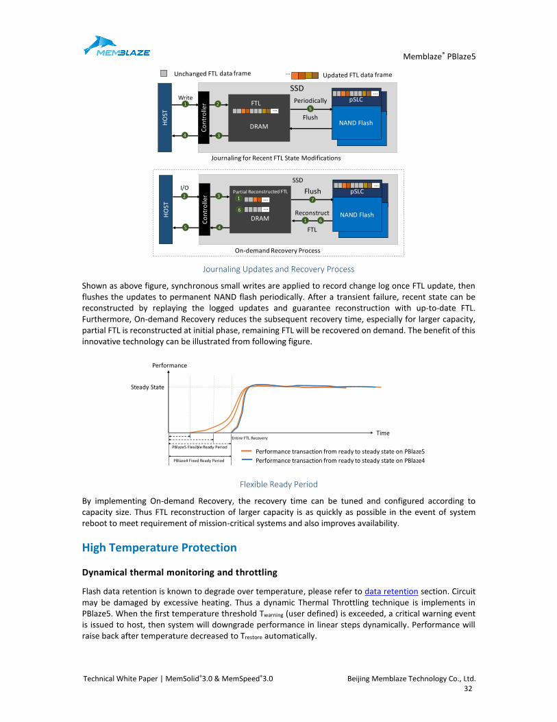
Memblaze® PBlaze5
Technical White Paper | MemSolid®3.0 & MemSpeed®3.0 Beijing Memblaze Technology Co., Ltd. 32
SSD
pSLC
3D TLC
On-demand Recovery Process
DRAM
Co
ntr
olle
r
pSLC
NAND Flash
···
Periodically
Flush
···
HO
ST
Write
SSD
pSLC
3D TLCDRAM
Co
ntr
olle
r
pSLC
NAND Flash
···
HO
ST
···
Journaling for Recent FTL State Modifications
I/O
1
4
52
3
45
2 3
Reconstruct
FTL
7
···
1 6
Flush
···
1
6
Journaling Updates and Recovery Process
Shown as above figure, synchronous small writes are applied to record change log once FTL update, then flushes the updates to permanent NAND flash periodically. After a transient failure, recent state can be reconstructed by replaying the logged updates and guarantee reconstruction with up-to-date FTL. Furthermore, On-demand Recovery reduces the subsequent recovery time, especially for larger capacity, partial FTL is reconstructed at initial phase, remaining FTL will be recovered on demand. The benefit of this innovative technology can be illustrated from following figure.
Performance
Steady State
Performance transaction from ready to steady state on PBlaze5
Performance transaction from ready to steady state on PBlaze4
Time
PBlaze5 Flexible Ready Period
PBlaze4 Fixed Ready Period
Entire FTL Recovery
Flexible Ready Period
By implementing On-demand Recovery, the recovery time can be tuned and configured according to capacity size. Thus FTL reconstruction of larger capacity is as quickly as possible in the event of system reboot to meet requirement of mission-critical systems and also improves availability.
High Temperature Protection
Dynamical thermal monitoring and throttling
Flash data retention is known to degrade over temperature, please refer to data retention section. Circuit may be damaged by excessive heating. Thus a dynamic Thermal Throttling technique is implements in PBlaze5. When the first temperature threshold Twarning (user defined) is exceeded, a critical warning event is issued to host, then system will downgrade performance in linear steps dynamically. Performance will raise back after temperature decreased to Trestore automatically.
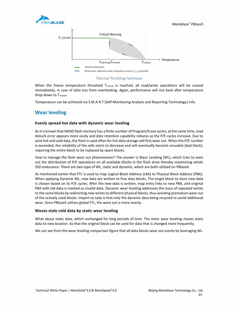
Memblaze® PBlaze5
Technical White Paper | MemSolid®3.0 & MemSpeed®3.0 Beijing Memblaze Technology Co., Ltd. 33
TcriticalTwarning/TrestoreTemperature
Critical WarningP_normal
Performance adjustment when temperature around Twarning threshold
Normal performance
Thermal Throttling Technique
When the freeze temperature threshold Tcritical is reached, all read/write operations will be ceased immediately, in case of data loss from overheating. Again, performance will rise back after temperature drop down to Trestore.
Temperature can be achieved via S.M.A.R.T (Self-Monitoring Analysis and Reporting Technology) info.
Wear leveling
Evenly spread hot data with dynamic wear leveling
As it is known that NAND flash memory has a finite number of Program/Erase cycles, at the same time, read disturb error appears more easily and data retention capability reduces as the P/E cycles increase. Due to exist hot and cold data, the flash is used often for hot data storage will first wear out. When the P/E number is exceeded, the reliability of the cells starts to decrease and will eventually become unusable (bad block), requiring the entire block to be replaced by spare blocks.
How to manage the flash wear out phenomenon? The answer is Wear Leveling (WL), which tries to even out the distribution of P/E operations on all available blocks in the flash drive thereby maximizing whole SSD endurance. There are two type of WL, static and dynamic, which are both utilized on PBlaze4.
As mentioned earlier that FTL is used to map Logical Block Address (LBA) to Physical Block Address (PBA). When applying Dynamic WL, new data are written to free data blocks. The target block to store new data is chosen based on its P/E cycles. After the new data is written, map entry links to new PBA, and original PBA with old data is marked as invalid data. Dynamic wear leveling addresses the issue of repeated writes to the same blocks by redirecting new writes to different physical blocks, thus avoiding premature wear out of the actively used blocks. Import to note is that only the dynamic data being recycled to avoid additional wear. Since PBlaze4 utilizes global FTL, the ware out is more evenly.
Moves stale cold data by static wear leveling
What about static data, which unchanged for long periods of time. The static wear leveling moves static data to new location. So that the original block can be used for data that is changed more frequently.
We can see from the wear leveling comparison figure that all data blocks wear out evenly by leveraging WL.
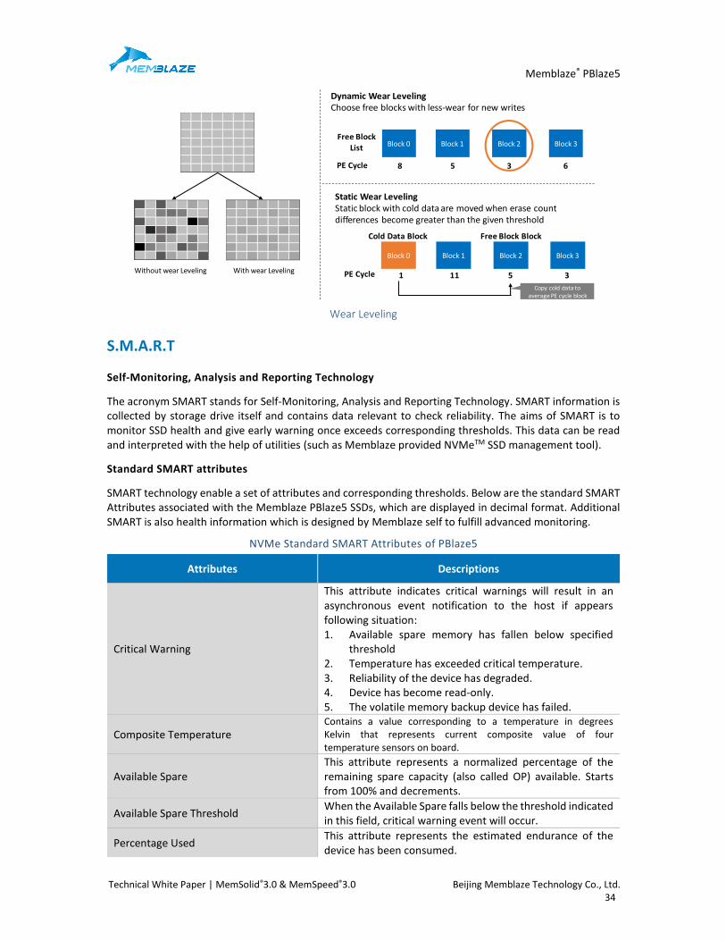
Memblaze® PBlaze5
Technical White Paper | MemSolid®3.0 & MemSpeed®3.0 Beijing Memblaze Technology Co., Ltd. 34
Dynamic Wear LevelingChoose free blocks with less-wear for new writes
Static Wear LevelingStatic block with cold data are moved when erase count differences become greater than the given threshold
Block 0 Block 1 Block 2 Block 3
Block 1 Block 2 Block 3Block 0
Copy cold data to average PE cycle block
Free Block
List
PE Cycle 8 5 3 6
PE Cycle
Cold Data Block
1 11 5 3
Free Block Block
Without wear Leveling With wear Leveling
Wear Leveling
S.M.A.R.T
Self-Monitoring, Analysis and Reporting Technology
The acronym SMART stands for Self-Monitoring, Analysis and Reporting Technology. SMART information is collected by storage drive itself and contains data relevant to check reliability. The aims of SMART is to monitor SSD health and give early warning once exceeds corresponding thresholds. This data can be read and interpreted with the help of utilities (such as Memblaze provided NVMeTM SSD management tool).
Standard SMART attributes
SMART technology enable a set of attributes and corresponding thresholds. Below are the standard SMART Attributes associated with the Memblaze PBlaze5 SSDs, which are displayed in decimal format. Additional SMART is also health information which is designed by Memblaze self to fulfill advanced monitoring.
NVMe Standard SMART Attributes of PBlaze5
Attributes Descriptions
Critical Warning
This attribute indicates critical warnings will result in an asynchronous event notification to the host if appears following situation: 1. Available spare memory has fallen below specified
threshold 2. Temperature has exceeded critical temperature. 3. Reliability of the device has degraded. 4. Device has become read-only. 5. The volatile memory backup device has failed.
Composite Temperature Contains a value corresponding to a temperature in degrees Kelvin that represents current composite value of four temperature sensors on board.
Available Spare This attribute represents a normalized percentage of the remaining spare capacity (also called OP) available. Starts from 100% and decrements.
Available Spare Threshold When the Available Spare falls below the threshold indicated in this field, critical warning event will occur.
Percentage Used This attribute represents the estimated endurance of the device has been consumed.
Memblaze® PBlaze5
Technical White Paper | MemSolid®3.0 & MemSpeed®3.0 Beijing Memblaze Technology Co., Ltd. 35
Attributes Descriptions
Data Units Read This attribute represents the number of 512 byte data units the host has read from the controller (this value does not include metadata).
Data Units Written This attribute represents the number of 512 byte data units the host has written to the controller (this value does not include metadata).
Host Read Commands This attribute represents the number of read commands completed by the controller.
Host Write Commands This attribute represents the number of write commands completed by the controller.
Controller Busy Time This attribute represents the amount of time the controller is busy with I/O commands.
Power Cycles This attribute represents the number of power cycles.
Power On Hours This attribute represents the number of power-on hours.
Unsafe Shutdowns This attribute represents the number of unsafe shutdowns. This count is incremented when a shutdown notification (CC.SHN) is not received prior to loss of power.
Media and Data Integrity Errors
This attribute represents the number of occurrences where the controller detected an unrecovered data integrity error. Errors such as uncorrectable ECC, CRC checksum failure, or LBA tag mismatch are included in this field.
Number of Error Information Log Entries This attribute represents the number of Error Information log entries over the life of the controller.
Temperature Sensor 1 Contains the current temperature in degrees Kelvin reported by the sensor in the controller (core sensor)
Temperature Sensor 2 Contains the current temperature in degrees Kelvin reported by the sensor besides the controller (board sensor)
Temperature Sensor 3 Contains the current temperature in degrees Kelvin reported by the NAND area sensor which is near the controller.
Temperature Sensor 4 Contains the current temperature in degrees Kelvin reported by the NAND area sensor which is far away from the controller.
PBlaze5 Provides Rich Enterprise-level Features
Whole Disk Encryption with AES-XTS 256-bit
Superior data protection with AES-XTS
Data loss is happening frequently and at an increasing rate around the world. The Advanced Encryption Standard (AES) is an encryption standard approved by the National Institute of Standards and Technology (NIST) for the safeguarding of electronic data. After being adopted by the US government, the standard is now used worldwide. This cipher is widely used to protect sensitive information and is found integrated at both the hardware and software level.
The most common forms of AES are AES-256 (encrypts data in 256 bit key sizes) and AES-128 (encrypts data in 128 bit key sizes). All user data written to PBlaze5 is secured with XTS 256-bit AES Hardware Encryption. Comparing with other block cipher mode of operation such as CBC (Cipher-Block chaining) and ECB (Electronic Codebook), XTS (XEX-based tweaked-codebook mode with ciphertext stealing) provides more protections, figure User Data Encryption clearly demonstrates that. The left one in the figure is unencrypted image, the image on the right shows the appearance of utilizing ECB and XTS mode. Due to the same image pixel in the encryption block which is encrypted by ECB will produce the same ciphertext, so the original image appears diafiltration phenomenon. Whereas, XTS ensures the same plaintext will not generate the

Memblaze® PBlaze5
Technical White Paper | MemSolid®3.0 & MemSpeed®3.0 Beijing Memblaze Technology Co., Ltd. 36
same ciphertext. Obviously, for enterprise users who have highly data security requirement, XTS shows essentially unbreakable data protection ability.
Original Image Encrypted with ECB Encrypted with XTS
User Data Encrypted with ECB & XTS Cipher Mode
How does AES-XTS work?
If think of encryption as an adapter, the data is encoded before being written or decoded before being read. XTS makes use of two different AES keys (Key1 and Key2), two keys are passed at different point to be used for the encryption/decryption. One for AES encryption, another performs "128bit tweak value" encryption. Tweak value encryption has been further modified by means of GF(X) and XOR, ensures the same user data will not generate the same cipher text. The AES Keys store at pSLC area with redundancy.
SSD
Controller
Host Memory
SSD
Raw data
Raw data
Without Encryption:
With Encryption: Host
Memory
Ingress DMA XTS-AES Encryption
Write: Raw data
Read: Raw data
NAND
Write: Encrypted data
Encrypted data
Plaintext: 128bitAES-enc: Standard AES algorithmKey1: Data encryption keytweak: 128bit tweak valueKey2: tweak encryption key
: GF(X) polynomialCiphertext: 128bit
Write
Read
AES-enc. AES-enc.
128-bit tweak
Key2 Key1
Plaintext
αj
Ciphertext
Egress DMA Decryption
NANDNAND
Data Encryption with XTS-AES-256
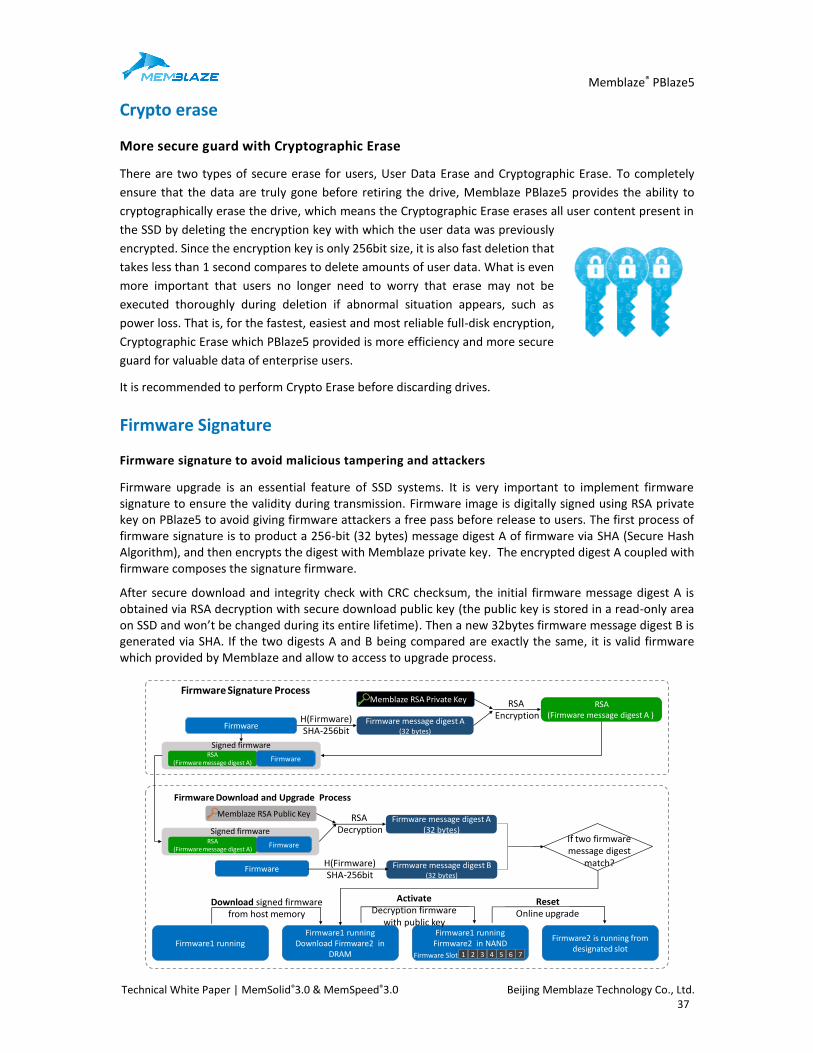
Memblaze® PBlaze5
Technical White Paper | MemSolid®3.0 & MemSpeed®3.0 Beijing Memblaze Technology Co., Ltd. 37
Crypto erase
More secure guard with Cryptographic Erase
There are two types of secure erase for users, User Data Erase and Cryptographic Erase. To completely
ensure that the data are truly gone before retiring the drive, Memblaze PBlaze5 provides the ability to
cryptographically erase the drive, which means the Cryptographic Erase erases all user content present in
the SSD by deleting the encryption key with which the user data was previously
encrypted. Since the encryption key is only 256bit size, it is also fast deletion that
takes less than 1 second compares to delete amounts of user data. What is even
more important that users no longer need to worry that erase may not be
executed thoroughly during deletion if abnormal situation appears, such as
power loss. That is, for the fastest, easiest and most reliable full-disk encryption,
Cryptographic Erase which PBlaze5 provided is more efficiency and more secure
guard for valuable data of enterprise users.
It is recommended to perform Crypto Erase before discarding drives.
Firmware Signature
Firmware signature to avoid malicious tampering and attackers
Firmware upgrade is an essential feature of SSD systems. It is very important to implement firmware signature to ensure the validity during transmission. Firmware image is digitally signed using RSA private key on PBlaze5 to avoid giving firmware attackers a free pass before release to users. The first process of firmware signature is to product a 256-bit (32 bytes) message digest A of firmware via SHA (Secure Hash Algorithm), and then encrypts the digest with Memblaze private key. The encrypted digest A coupled with firmware composes the signature firmware.
After secure download and integrity check with CRC checksum, the initial firmware message digest A is obtained via RSA decryption with secure download public key (the public key is stored in a read-only area on SSD and won’t be changed during its entire lifetime). Then a new 32bytes firmware message digest B is generated via SHA. If the two digests A and B being compared are exactly the same, it is valid firmware which provided by Memblaze and allow to access to upgrade process.
Firmware Download and Upgrade Process
Firmware Signature Process
Signed firmware
Firmware1 runningFirmware1 running
Download Firmware2 in DRAM
Firmware1 runningFirmware2 in NAND
Firmware2 is running from designated slot
Download signed firmware from host memory
ActivateDecryption firmware
with public key
ResetOnline upgrade
1 2 3 4 5 6 7Firmware Slot
Memblaze RSA Private Key
Firmware
RSA(Firmware message digest A )
RSA Encryption
RSA(Firmware message digest A)
Firmware
Firmware message digest A(32 bytes)
H(Firmware)SHA-256bit
Signed firmwareRSA
(Firmware message digest A)Firmware
Memblaze RSA Public Key RSA Decryption
Firmware message digest A(32 bytes)
If two firmware message digest
match?Firmware Firmware message digest B
(32 bytes)
H(Firmware)SHA-256bit
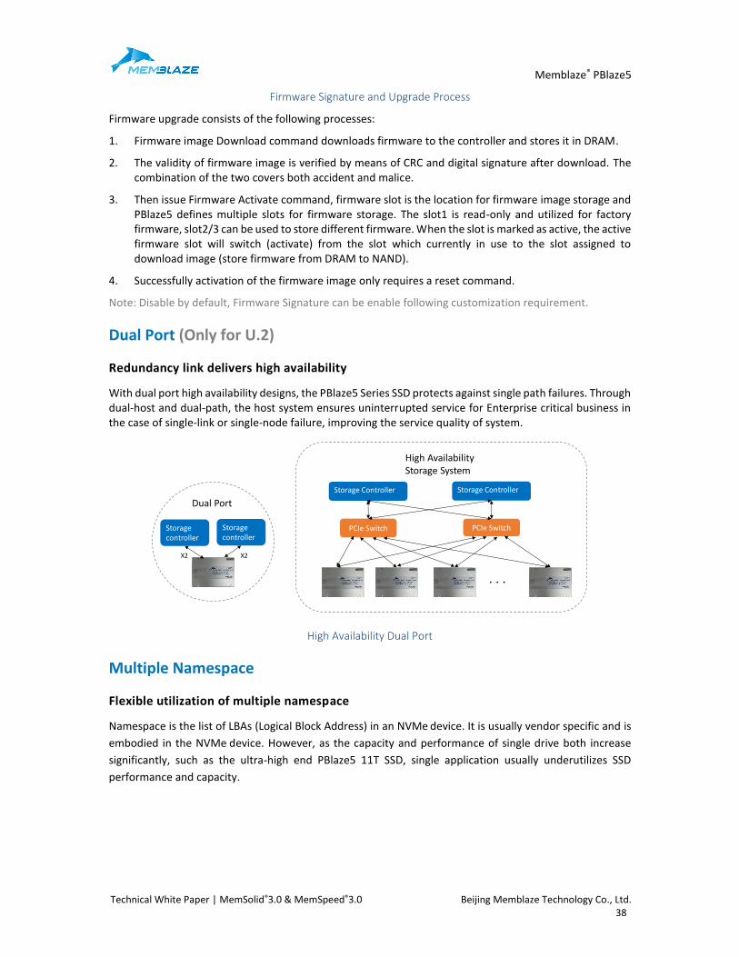
Memblaze® PBlaze5
Technical White Paper | MemSolid®3.0 & MemSpeed®3.0 Beijing Memblaze Technology Co., Ltd. 38
Firmware Signature and Upgrade Process
Firmware upgrade consists of the following processes:
1. Firmware image Download command downloads firmware to the controller and stores it in DRAM.
2. The validity of firmware image is verified by means of CRC and digital signature after download. The combination of the two covers both accident and malice.
3. Then issue Firmware Activate command, firmware slot is the location for firmware image storage and PBlaze5 defines multiple slots for firmware storage. The slot1 is read-only and utilized for factory firmware, slot2/3 can be used to store different firmware. When the slot is marked as active, the active firmware slot will switch (activate) from the slot which currently in use to the slot assigned to download image (store firmware from DRAM to NAND).
4. Successfully activation of the firmware image only requires a reset command.
Note: Disable by default, Firmware Signature can be enable following customization requirement.
Dual Port (Only for U.2)
Redundancy link delivers high availability
With dual port high availability designs, the PBlaze5 Series SSD protects against single path failures. Through dual-host and dual-path, the host system ensures uninterrupted service for Enterprise critical business in the case of single-link or single-node failure, improving the service quality of system.
Storage controller
Storage controller
Dual Port
X2 X2
. . .
PCIe Switch PCIe Switch
Storage Controller Storage Controller
High Availability Storage System
High Availability Dual Port
Multiple Namespace
Flexible utilization of multiple namespace
Namespace is the list of LBAs (Logical Block Address) in an NVMe device. It is usually vendor specific and is
embodied in the NVMe device. However, as the capacity and performance of single drive both increase
significantly, such as the ultra-high end PBlaze5 11T SSD, single application usually underutilizes SSD
performance and capacity.
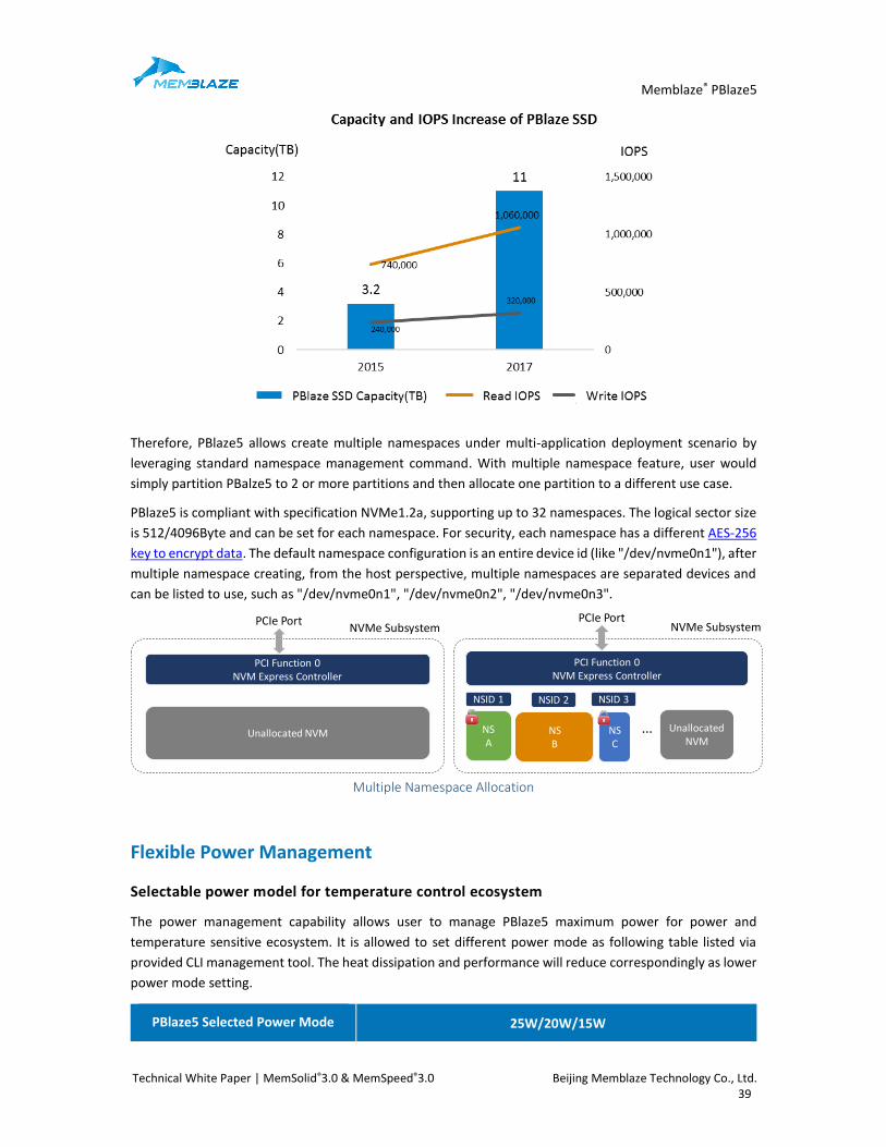
Memblaze® PBlaze5
Technical White Paper | MemSolid®3.0 & MemSpeed®3.0 Beijing Memblaze Technology Co., Ltd. 39
Therefore, PBlaze5 allows create multiple namespaces under multi-application deployment scenario by
leveraging standard namespace management command. With multiple namespace feature, user would
simply partition PBalze5 to 2 or more partitions and then allocate one partition to a different use case.
PBlaze5 is compliant with specification NVMe1.2a, supporting up to 32 namespaces. The logical sector size
is 512/4096Byte and can be set for each namespace. For security, each namespace has a different AES-256
key to encrypt data. The default namespace configuration is an entire device id (like "/dev/nvme0n1"), after
multiple namespace creating, from the host perspective, multiple namespaces are separated devices and
can be listed to use, such as "/dev/nvme0n1", "/dev/nvme0n2", "/dev/nvme0n3".
PCI Function 0NVM Express Controller
NSID 1 NSID 2
NS A
NSID 3
···NS B
NS C
Unallocated NVM
PCIe PortNVMe Subsystem
PCI Function 0NVM Express Controller
Unallocated NVM
PCIe PortNVMe Subsystem
Multiple Namespace Allocation
Flexible Power Management
Selectable power model for temperature control ecosystem
The power management capability allows user to manage PBlaze5 maximum power for power and
temperature sensitive ecosystem. It is allowed to set different power mode as following table listed via
provided CLI management tool. The heat dissipation and performance will reduce correspondingly as lower
power mode setting.
PBlaze5 Selected Power Mode 25W/20W/15W
Memblaze® PBlaze5
Technical White Paper | MemSolid®3.0 & MemSpeed®3.0 Beijing Memblaze Technology Co., Ltd. 40
Summary
Memblaze’s premium enterprise-class PBlaze5 SSD Series portfolio are cutting-edge PCIe/NVMeTM drives with exceptional performance and lowest latency, coupled with new implemented reliability technologies for read-intensive, mixed workload and write intensive applications galore in data centers.
Additional information on the PBlaze5 Series, as well as Memblaze’s complete line-up of enterprise SSDs and software solutions are available at www.memblaze.com.
Memblaze® PBlaze5
Technical White Paper | MemSolid®3.0 & MemSpeed®3.0 Beijing Memblaze Technology Co., Ltd. 41
Reference
Some industry definitions and terms for this white paper were referenced from a host of reputable industry resources that included, but not limited to:
Gartner Research www.gartner.com
Wikibon www.wikibon.com
PMC-SIERRA www.pmcs.com
IDC Research www.idc.com
Intel www.intel.com
JEDEC www.jedec.org
NVMeTM www.nvmexpress.org
Wikipedia www.wikipedia.com
Oracle www.oracle.com
Micron https://www.micron.com/products/nand-flash
NVM Express 1.2 http://nvmexpsress.org/wp-content/uploads/NVM_Express_1_2_Gold_20141209.pdf
TechTarget http://searchsolidstatestorage.techtarget.com/resources/Solid-state-storage-technology
“Threshold Voltage Distribution in MLC NAND Flash Memory: Characterization, Analysis, and Modeling”
“LDPC-in-SSD: Making Advanced Error Correction Codes Work Effectively in Solid State Drives”
“Atomic Writes for data integrity and consistency in shared storage devices for clusters. “ Michael Okun and Amnon Barak, Future Generation Computer Systems
ACID http://searchsqlserver.techtarget.com/definition/ACID
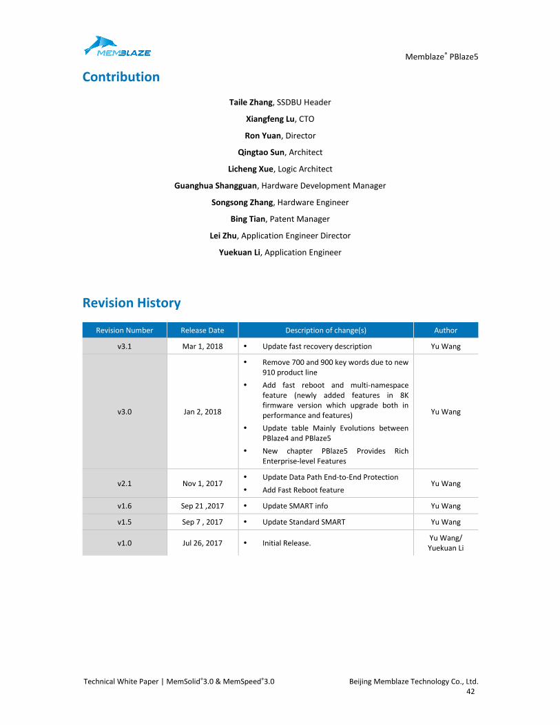
Memblaze® PBlaze5
Technical White Paper | MemSolid®3.0 & MemSpeed®3.0 Beijing Memblaze Technology Co., Ltd. 42
Contribution
Taile Zhang, SSDBU Header
Xiangfeng Lu, CTO
Ron Yuan, Director
Qingtao Sun, Architect
Licheng Xue, Logic Architect
Guanghua Shangguan, Hardware Development Manager
Songsong Zhang, Hardware Engineer
Bing Tian, Patent Manager
Lei Zhu, Application Engineer Director
Yuekuan Li, Application Engineer
Revision History
Revision Number Release Date Description of change(s) Author
v3.1 Mar 1, 2018 Update fast recovery description Yu Wang
v3.0 Jan 2, 2018
Remove 700 and 900 key words due to new 910 product line
Add fast reboot and multi-namespace feature (newly added features in 8K firmware version which upgrade both in performance and features)
Update table Mainly Evolutions between PBlaze4 and PBlaze5
New chapter PBlaze5 Provides Rich Enterprise-level Features
Yu Wang
v2.1 Nov 1, 2017 Update Data Path End-to-End Protection
Add Fast Reboot feature Yu Wang
v1.6 Sep 21 ,2017 Update SMART info Yu Wang
v1.5 Sep 7 , 2017 Update Standard SMART Yu Wang
v1.0 Jul 26, 2017 Initial Release. Yu Wang/ Yuekuan Li

Memblaze® PBlaze5
Technical White Paper | MemSolid®3.0 & MemSpeed®3.0 Beijing Memblaze Technology Co., Ltd. 43
About Memblaze
Founded in 2011 and based in Beijing, Memblaze is a technological company with innovative genes. It focuses on providing outstanding enterprise-level solid-state drives and solutions in fields such as IT, Internet, Communication and Cloud Computing.
For more information, please visit: www.memblaze.com [email protected]
DISCLAIMER
Information in this document is provided in connection with Memblaze products. Memblaze provides this document “as is”, without warranty of any kind, neither expressed nor implied, including, but not limited to, the particular purpose. Memblaze may make improvements and/or changes in this document or in the product described in this document at any time without notice. The products described in this document may contain design defects or errors known as anomalies or errata which may cause the products functions to deviate from published specifications.
COPYRIGHT
© 2017 Memblaze Corp. All rights reserved. No part of this document may be reproduced, transmitted, transcribed, stored in a retrieval system, or translated into any language in any form or by any means without the written permission of Memblaze Corp.
TRADEMARKS
Memblaze is a trademark of Memblaze Corporation. Other names mentioned in this document are trademarks/registered trademarks of their respective owners.
USING THIS DOCUMENT
Though Memblaze has reviewed this document and very effort has been made to ensure that this document is current and accurate, more information may have become available subsequent to the production of this guide. In that event, please contact your local Memblaze sales office or your distributor for latest specifications before placing your product order.
Recommended