EE130 Lecture 18, Slide 1Spring 2007
Lecture #18
OUTLINE
• pn junctions (cont’d)
– Deviations from the ideal I-V R-G current series resistance high-level injection
– Narrow-base diode
Reading: Chapter 6.2, 6.3

EE130 Lecture 18, Slide 2Spring 2007
Effect of R-G in Depletion Region
• The net generation rate is given by
• R-G in the depletion region contributes an additional component of diode current IR-G
levelenergy state- trap
and where
)(τ)(τ/)(
1/)(
1
11
2
T
kTEEi
kTEEi
np
i
E
enpenn
ppnn
npn
t
n
t
p
TiiT
dxt
pqAI
GR
x
xGR
n
p
EE130 Lecture 18, Slide 3Spring 2007
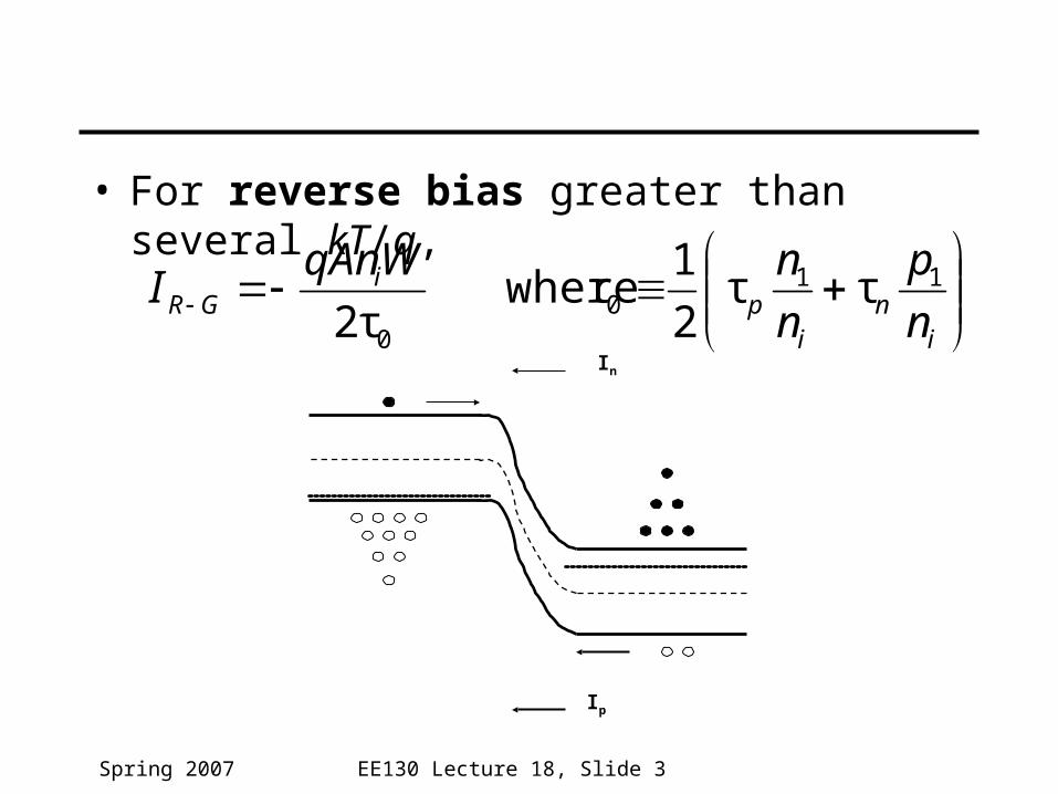
• For reverse bias greater than several kT/q,
in
ip
iGR n
p
n
nWqAnI 11
00
ττ2
1 τ where
τ2
Ip
In
EE130 Lecture 18, Slide 4Spring 2007
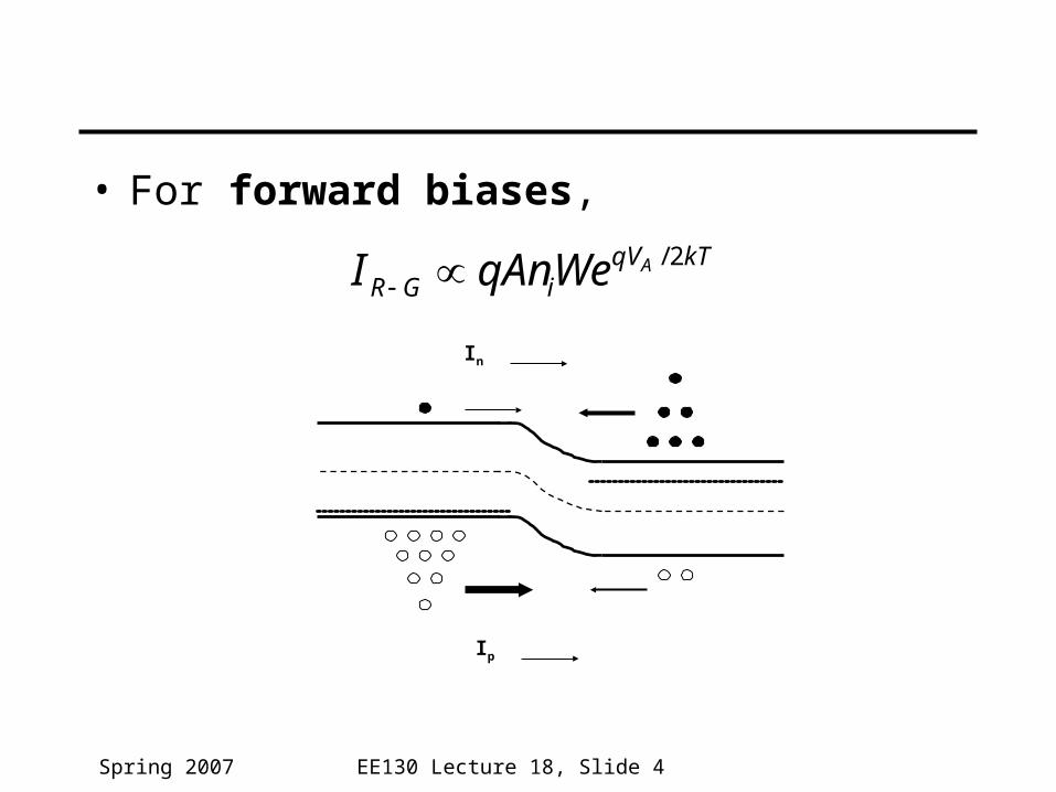
• For forward biases,
kTqViGR
AWeqAnI 2/
Ip
In
EE130 Lecture 18, Slide 5Spring 2007
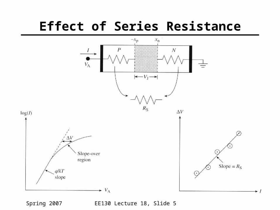
Effect of Series Resistance

EE130 Lecture 18, Slide 6Spring 2007
High-Level Injection Effect
• As VA increases, the side of the junction which is more lightly doped will eventually reach HLI:
significant gradient in majority-carrier profile
Majority-carrier diffusion current reduces the diode current from the ideal
pop
non
pp
nn
or
(p+n junction)
(n+p junction)
EE130 Lecture 18, Slide 7Spring 2007
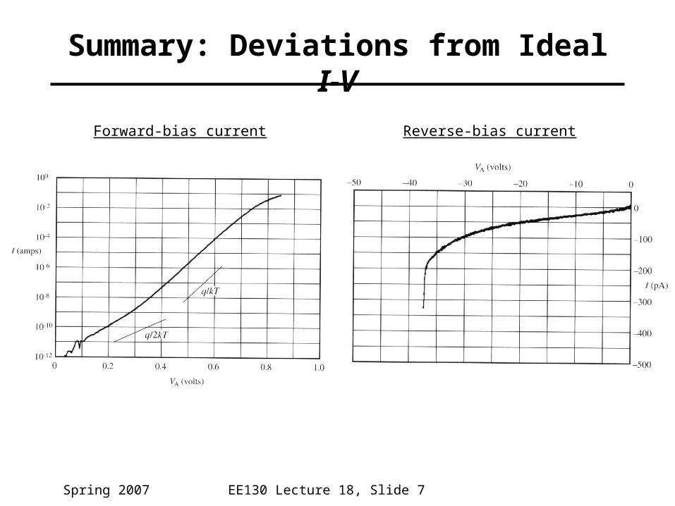
Summary: Deviations from Ideal I-V
Forward-bias current Reverse-bias current

EE130 Lecture 18, Slide 8Spring 2007
Derivation of Narrow-Base Diode I-V
• We have the following boundary conditions:
• With the following coordinate system:
• Then, the solution is of the form:
0)''( cn xxp)1()( / kTqVnonn
Aepxp
pp LxLx eAeAxp /2
/1)(
NEW:x' 0 0 x' '
x' c
EE130 Lecture 18, Slide 9Spring 2007
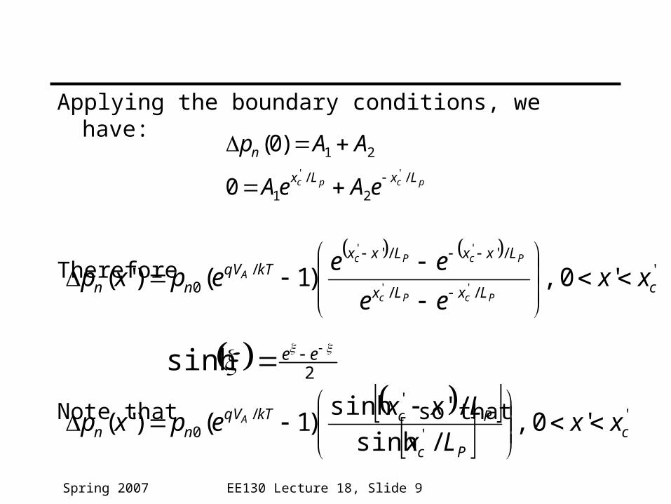
Applying the boundary conditions, we have:
Therefore
Note that so that
'
//
/'/'/
0 '0 ,)1()'( ''
''
cLxLx
LxxLxxkTqV
nn xxee
eeepxp
PcPc
PcPc
A
pcpc LxLx
n
eAeA
AAp/
2/
1
21
''
0
)0(
2sinh ee
''
'/
0 '0 ,/sinh
/'sinh)1()'( c
Pc
PckTqVnn xx
Lx
Lxxepxp A

EE130 Lecture 18, Slide 10Spring 2007
Excess Carrier Profiles: Limiting Cases
Long base (xc’):
pA
PcPc
pPcpPc
A
PcPc
PcPc
A
LxkTqVn
LxLx
LxLxLxLxkTqV
n
LxLx
LxxLxxkTqV
nn
eep
ee
eeeeep
ee
eeepxp
/'/0
//
/'//'//
0
//
/'/'/
0
)1(
)1(
)1()'(
''
''
''
''

EE130 Lecture 18, Slide 11Spring 2007
Narrow base (xc’0):
pn is a linear function of x
Jp is constant (no recombination)
'/
0'
'/
0
'
'/
0
'1)1(
/
/')1(
/sinh
/'sinh)1()'(
A
A
c
kTqVn
Pc
PckTqVn
Pc
PckTqVnn
x
xep
Lx
Lxxep
Lx
Lxxepxp
A
EE130 Lecture 18, Slide 12Spring 2007
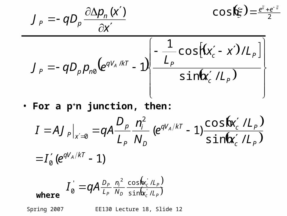
• For a p+n junction, then:
where
)1(
/sinh
/cosh)1(
0
2
0
kTVq
Pc
PckTVq
D
i
P
p
xP
A
A
eI
Lx
Lxe
N
n
L
DqAJAI
Pc
Pc
D
i
P
P
Lx
LxNn
LDqAI
/sinh
/cosh'0 '
'2
Pc
PcPkTqV
npP
npP
Lx
LxxL
epqDJ
x
xpqDJ
A
/sinh
/cosh1
1
)(
/0
2cosh ee
EE130 Lecture 18, Slide 13Spring 2007
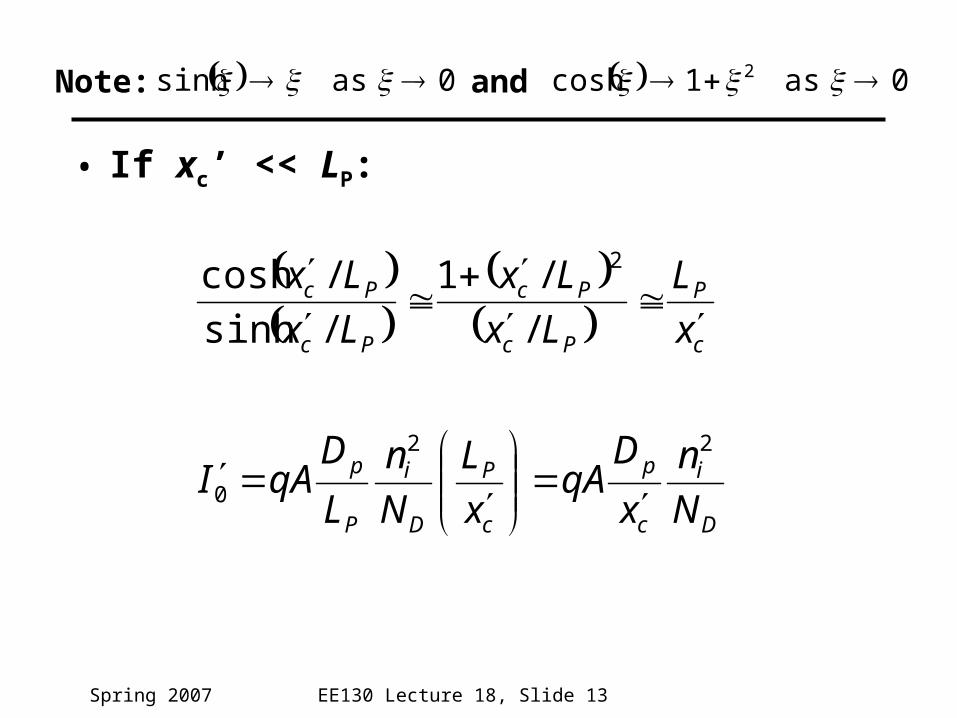
0 as sinh Note: 0 as 1cosh 2
• If xc’ << LP:
and
D
i
c
p
c
P
D
i
P
p
c
P
Pc
Pc
Pc
Pc
N
n
x
DqA
x
L
N
n
L
DqAI
x
L
Lx
Lx
Lx
Lx
22
0
2
/
/1
/sinh
/cosh
EE130 Lecture 18, Slide 14Spring 2007
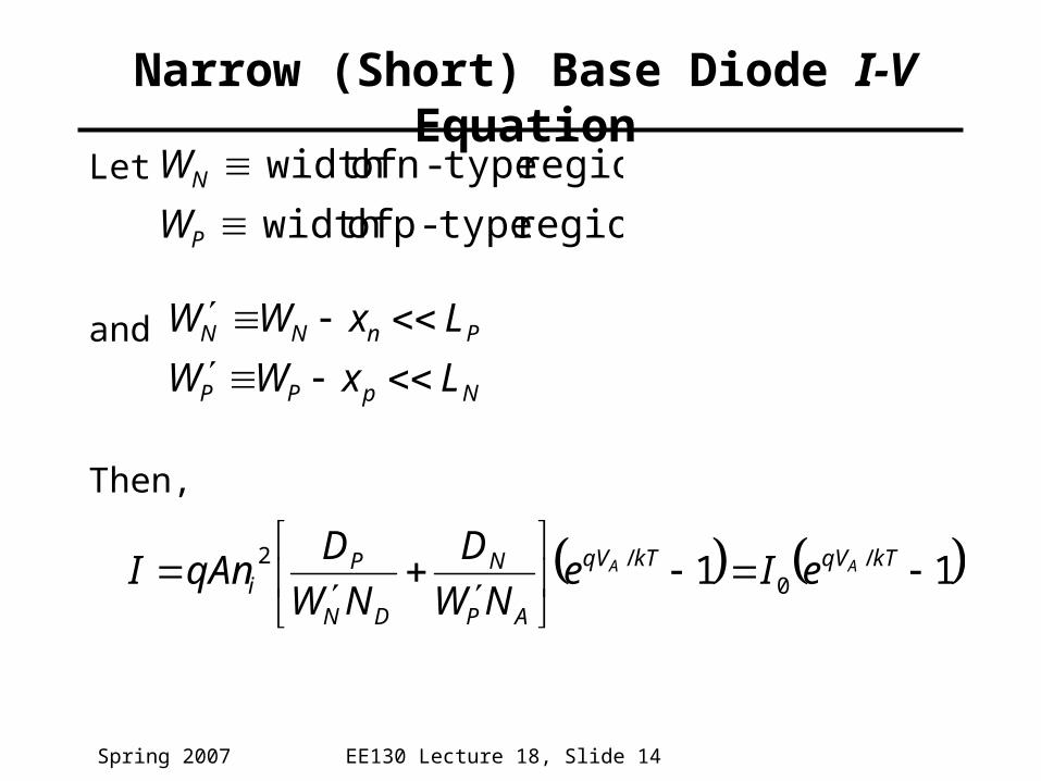
Narrow (Short) Base Diode I-V Equation
Let
and
Then,
region type-p of width
region type-n of width
P
N
W
W
NpPP
PnNN
LxWW
LxWW
11 /0
/2
kTqVkTqV
AP
N
DN
Pi
AA eIeNW
D
NW
DqAnI

EE130 Lecture 18, Slide 15Spring 2007
Summary: Current Flow in pn Junctions
• The diode current is dominated by the term associated with the more lightly doped side:
p+n diode:
pn+ diode:
i.e. current flowing across junction is dominated by carriers injected from the more heavily doped side
sidenshort
siden long
)( 2
2
0
DN
Pi
DP
Pi
nP
NW
DqAn
NL
DqAn
xII
sidepshort
sidep long
)(2
2
0
AP
Ni
AN
Ni
pN
NW
DqAn
NL
DqAn
xII
Recommended