Solid State Detectors
=
Semi-Conductor based Detectors
• Materials and their properties
• Energy bands and electronic structure
• Charge transport and conductivity
• Boundaries: the p-n junction
• Charge collection
• Energy and time resolution
• Radiation damage

Any form of elementary excitation can be used to detectthe radiation signal
Signal Generation Needs transfer of Energy
An electrical signal is generated by ionization: Incidentradiation quanta transfer sufficient energy to form electron-hole pairs
Other detection mechanisms are:
Excitation of optical states (scintillators)
Excitation of lattice vibrations (phonons)
Breakup of Cooper pairs in superconductors
Typical excitation energies:
Ionization in semiconductors: 1 – 5 eV
Scintillation: appr. 20 eV
Phonons: meV
Breakup of Cooper pairs: meV
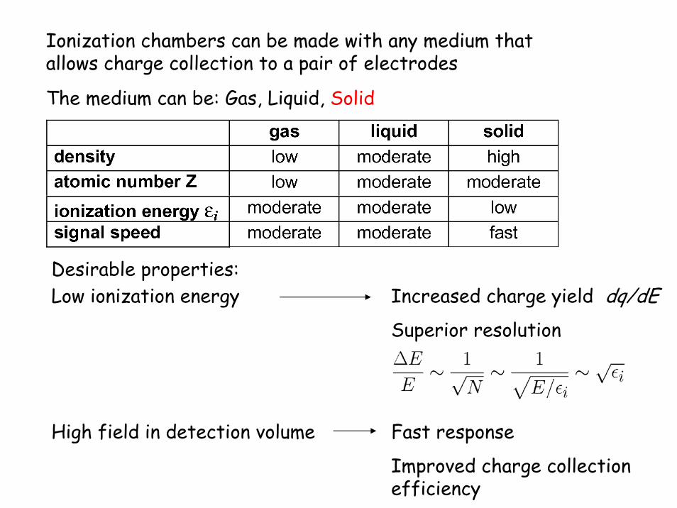
Ionization chambers can be made with any medium thatallows charge collection to a pair of electrodes
Desirable properties:
The medium can be: Gas, Liquid, Solid
Low ionization energy Increased charge yield dq/dESuperior resolution
High field in detection volume Fast response
Improved charge collectionefficiency
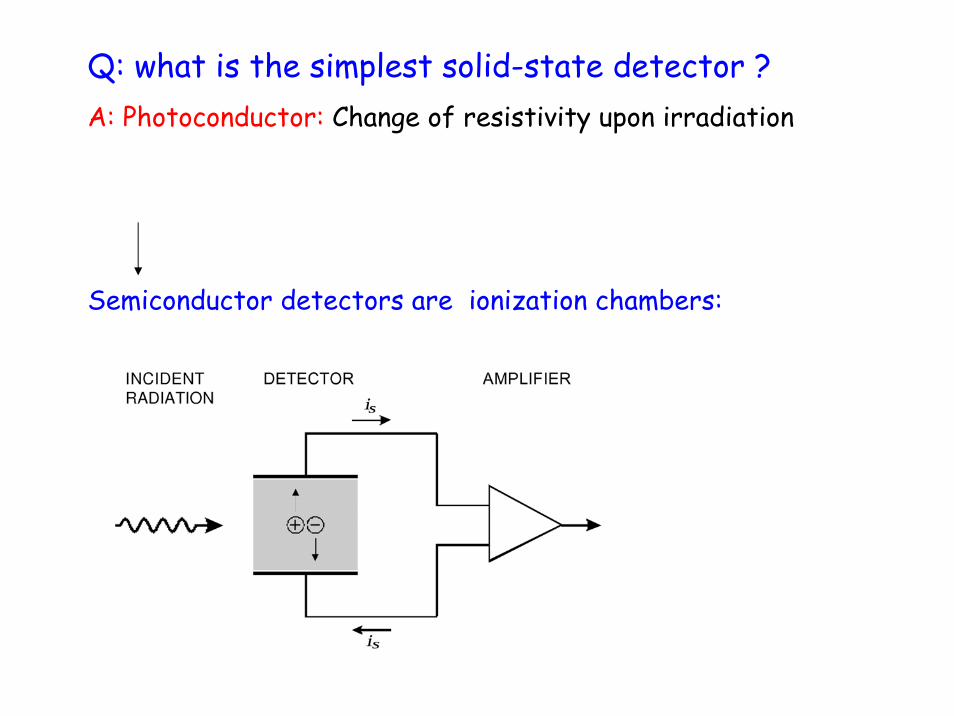
Q: what is the simplest solid-state detector ?A: Photoconductor: Change of resistivity upon irradiation
Semiconductor detectors are ionization chambers:

Semiconductor crystalsLattice structure of diamond, Si, Ge (Diamond structure)
a = Lattice constant Diamond: a = 0.356 nmGe: a = 0.565 nmSi: a = 0.543 nm
The crystalline structureleads to formation of electronic bandgaps

Creation of electron-hole pairsUpon absorption of a photon, a bondcan be broken which
excites an electron intothe conduction band and
leaves a vacant state in the valence band
The electron can movefreely
The hole is filled by a nearby electron, thusmoving to anotherposition
Holes behave like positive chargecarriers. They move more slowly becausehole transport involves many particles

Classification of Conductivity
Si, Ge Diamond
Conduction band
Conduction band
Conduction band
Valence band Valence band Valence band
Conductor Semiconductor Insulator
EΔE < 2 – 3 eV
ΔE > 5 eV

Ge Si GaAs
Eg = 0.7 eV Eg = 1.1 eV Eg = 1.4 eV
Indirect band gap Direct band gap
Band structure (3)
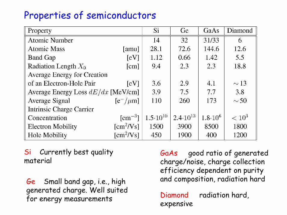
Properties of semiconductors
Si Currently best qualitymaterial
Ge Small band gap, i.e., high generated charge. Well suitedfor energy measurements
GaAs good ratio of generatedcharge/noise, charge collectionefficiency dependent on purityand composition, radiation hard
Diamond radiation hard, expensive

Energy required for creation of an electron-hole pair
C. A. Klein, J. Appl. Phys. 39,2029 (1968)
Ionization Energy > Band Gap
Formation of e-h pairsrequires both
1) Conservation of energy
2) Conservation of momentum
additional energyexcites phonons
εi=C1 + C2*Eg
Independent of material and type of radiation
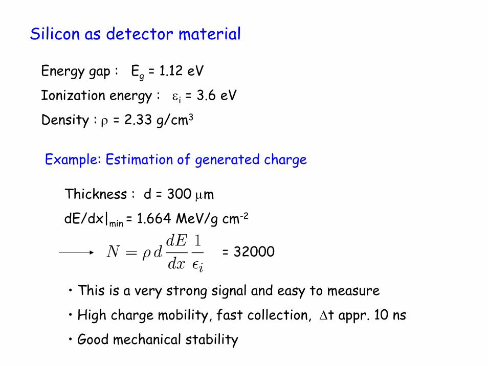
Silicon as detector material
Energy gap : Eg = 1.12 eV
Ionization energy : εi = 3.6 eV
Density : ρ = 2.33 g/cm3
Example: Estimation of generated charge
Thickness : d = 300 μm
dE/dx|min = 1.664 MeV/g cm-2
= 32000
• This is a very strong signal and easy to measure
• High charge mobility, fast collection, Δt appr. 10 ns
• Good mechanical stability
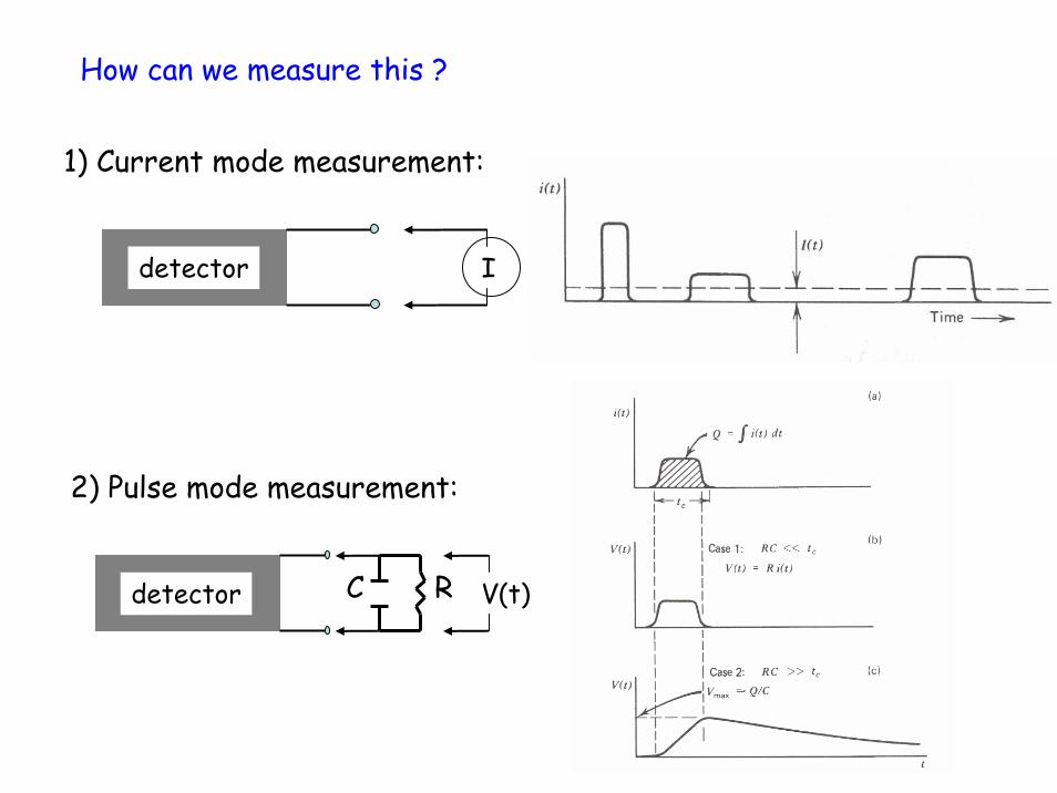
How can we measure this ?
1) Current mode measurement:
detector C R V(t)
detector I
2) Pulse mode measurement:
Intermezzo:what is the “Fano-Factor” ?
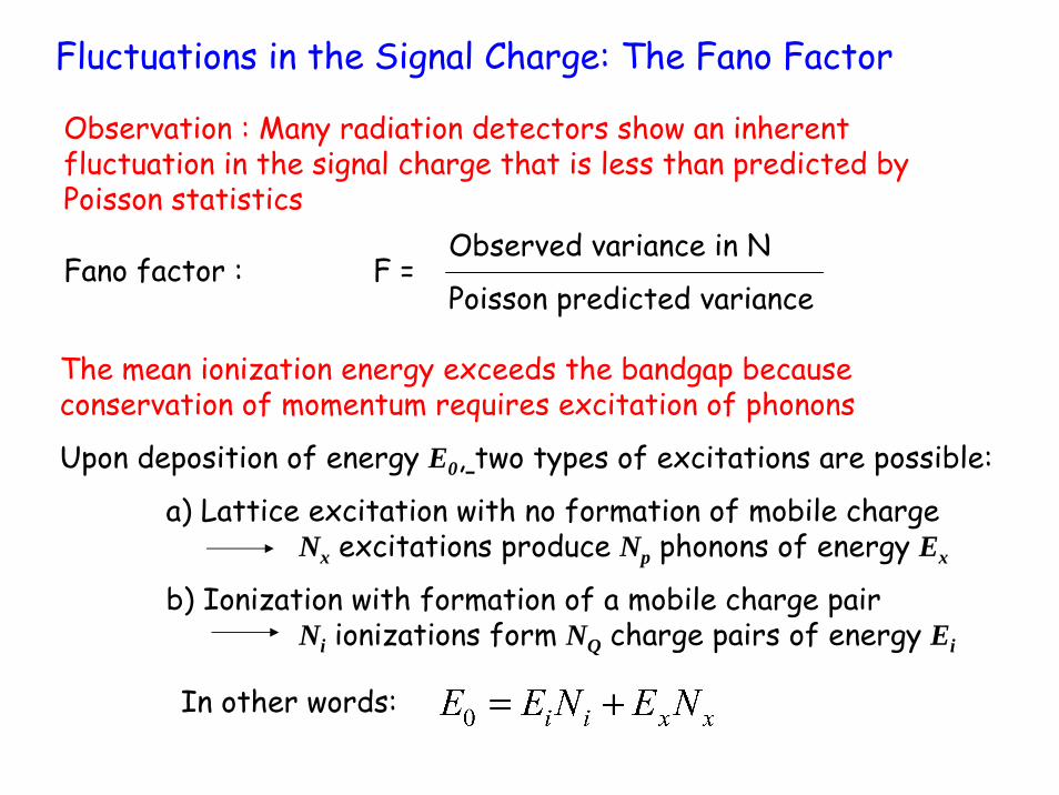
Fluctuations in the Signal Charge: The Fano Factor
The mean ionization energy exceeds the bandgap becauseconservation of momentum requires excitation of phonons
Upon deposition of energy E0, two types of excitations are possible:
a) Lattice excitation with no formation of mobile chargeNx excitations produce Np phonons of energy Ex
b) Ionization with formation of a mobile charge pairNi ionizations form NQ charge pairs of energy Ei
In other words:
Observation : Many radiation detectors show an inherentfluctuation in the signal charge that is less than predicted byPoisson statistics
Fano factor :Observed variance in N
Poisson predicted varianceF =
With (assuming Gaussian statistics)
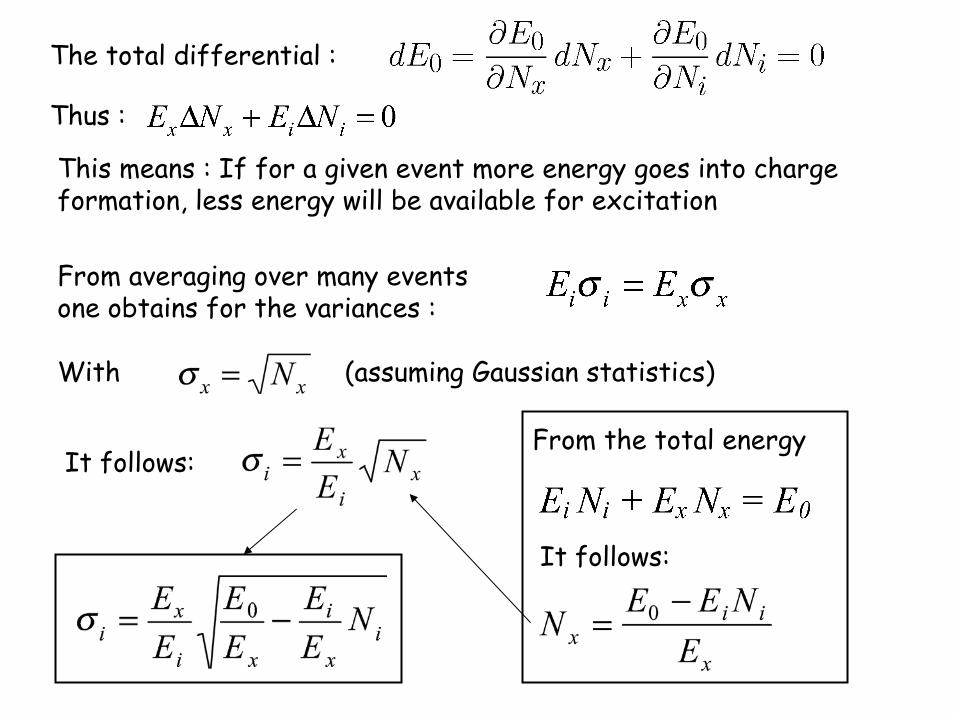
The total differential :
This means : If for a given event more energy goes into chargeformation, less energy will be available for excitation
From averaging over many eventsone obtains for the variances :
From the total energy
It follows:
It follows:
Thus :
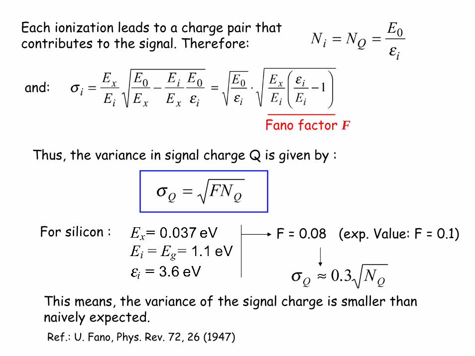
Each ionization leads to a charge pair thatcontributes to the signal. Therefore:
and:
Fano factor F
Thus, the variance in signal charge Q is given by :
For silicon : F = 0.08 (exp. Value: F = 0.1)
This means, the variance of the signal charge is smaller thannaively expected.Ref.: U. Fano, Phys. Rev. 72, 26 (1947)

End Intermezzo:what is the “Fano-Factor” ?
Bottom line:
QQ N=σOnly if all generated electron-holepairs were independent:
But they all originate from the same event cannot be independent variance smaller
this is material dependent!
QQ NF ×=σWith F smaller than 1.

Q: If a detector is this simple:
detector C R V(t)
why do we need so many expensive people ?
A: Because this photoconductor detector does not do the job!
Q: Why not?
A: Thermally generated dark current >> signal current !

Charge Carrier Density
Thermally activated charge carriers in the conduction band
Their density is given by
at room temperature
In a typical Si detector volume one obtains 4.5 x 10⁸ freecarriers compared to 3.2 x 10⁴ e-h pairs for MIP
For a detection of such an event, the number of freecarriers has to be substantially reduced.
This can be achieved via
a) cooling
b) pn-junction in reverse bias
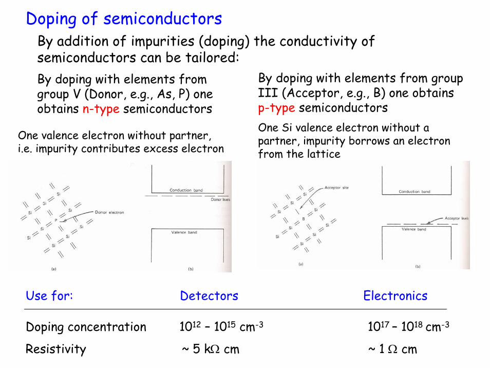
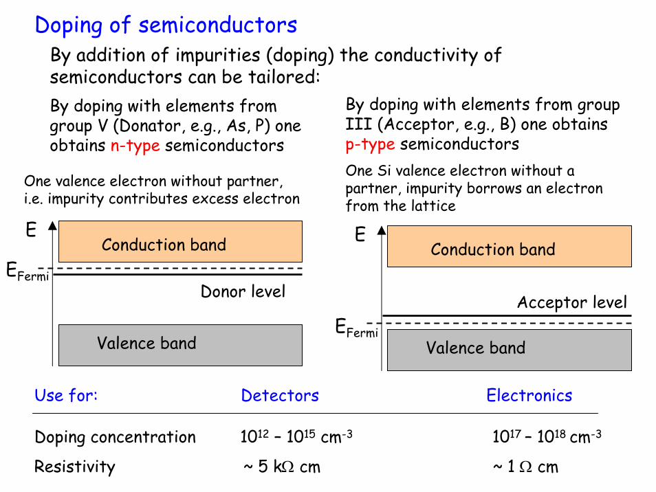
Doping of semiconductorsBy addition of impurities (doping) the conductivity of semiconductors can be tailored:By doping with elements fromgroup V (Donor, e.g., As, P) oneobtains n-type semiconductors
By doping with elements from groupIII (Acceptor, e.g., B) one obtainsp-type semiconductors
Use for: Detectors Electronics
Doping concentration 1012 – 1015 cm-3 1017 – 1018 cm-3
Resistivity ~ 5 kΩ cm ~ 1 Ω cm
One valence electron without partner, i.e. impurity contributes excess electron
One Si valence electron without a partner, impurity borrows an electronfrom the lattice
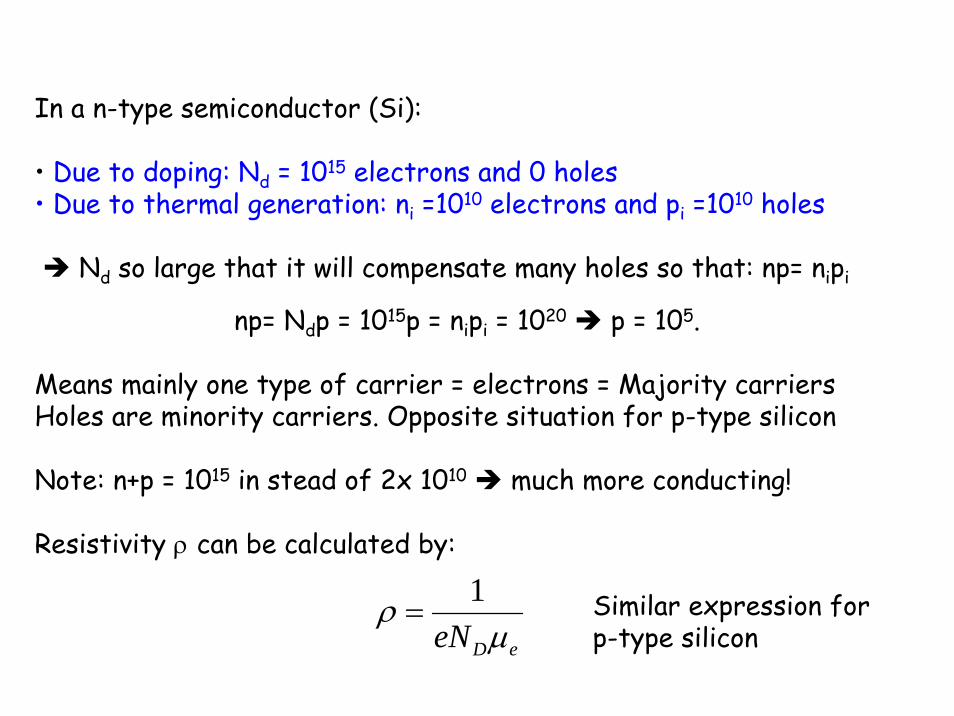
In a n-type semiconductor (Si):
• Due to doping: Nd = 1015 electrons and 0 holes• Due to thermal generation: ni =1010 electrons and pi =1010 holes
Nd so large that it will compensate many holes so that: np= nipi
np= Ndp = 1015p = nipi = 1020 p = 105.
Means mainly one type of carrier = electrons = Majority carriersHoles are minority carriers. Opposite situation for p-type silicon
Note: n+p = 1015 in stead of 2x 10¹⁰ much more conducting!
Resistivity ρ can be calculated by:
eDeN μρ 1= Similar expression for
p-type silicon
Doping of semiconductorsBy addition of impurities (doping) the conductivity of semiconductors can be tailored:By doping with elements fromgroup V (Donator, e.g., As, P) oneobtains n-type semiconductors
By doping with elements from groupIII (Acceptor, e.g., B) one obtainsp-type semiconductors
Conduction band
Valence band
Donor level
E
EFermi
Conduction band
Valence band
Acceptor level
E
EFermi
Use for: Detectors Electronics
Doping concentration 1012 – 1015 cm-3 1017 – 1018 cm-3
Resistivity ~ 5 kΩ cm ~ 1 Ω cm
One valence electron without partner, i.e. impurity contributes excess electron
One Si valence electron without a partner, impurity borrows an electronfrom the lattice

The p-n junction (1)Donor region and acceptor region adjoin each other :
n-typep-type
Thermal diffusion drives holes and electrons across thejunction
Electrons diffuse from the n- to the p-region, leaving a net positive space charge in the n-region and building up a potential (similar process for the holes)
The diffusion depth is limited when the space chargepotential energy exceeds the energy for thermal diffusion
Due to preparation conditions (implantation), the p-n junction is often highly asymmetric

The p-n junction (2)
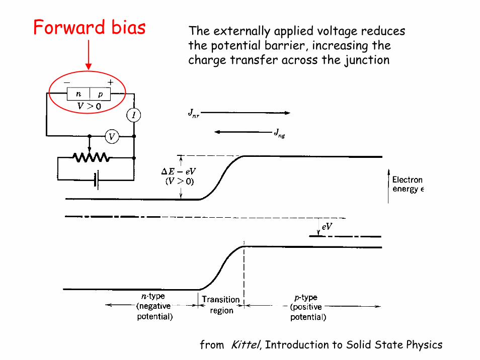
Forward bias
from Kittel, Introduction to Solid State Physics
The externally applied voltage reducesthe potential barrier, increasing thecharge transfer across the junction
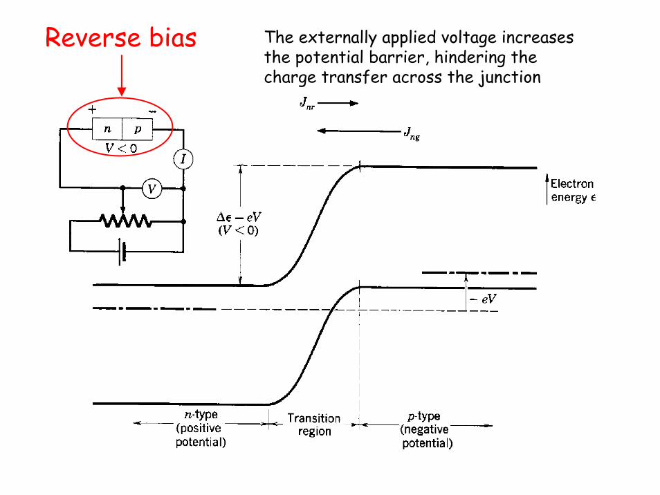
Reverse bias The externally applied voltage increasesthe potential barrier, hindering thecharge transfer across the junction

Diode current vs. voltage
Shockley equation
from Sze, Physics of Semiconductor Devices
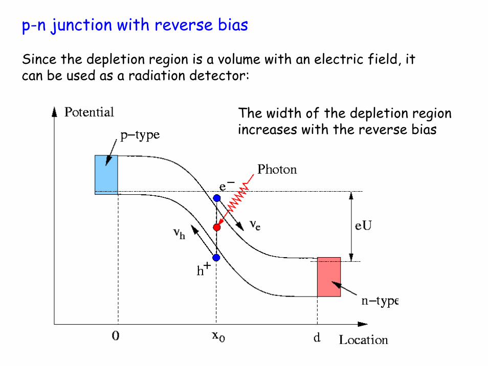
p-n junction with reverse bias
Since the depletion region is a volume with an electric field, itcan be used as a radiation detector:
The width of the depletion regionincreases with the reverse bias
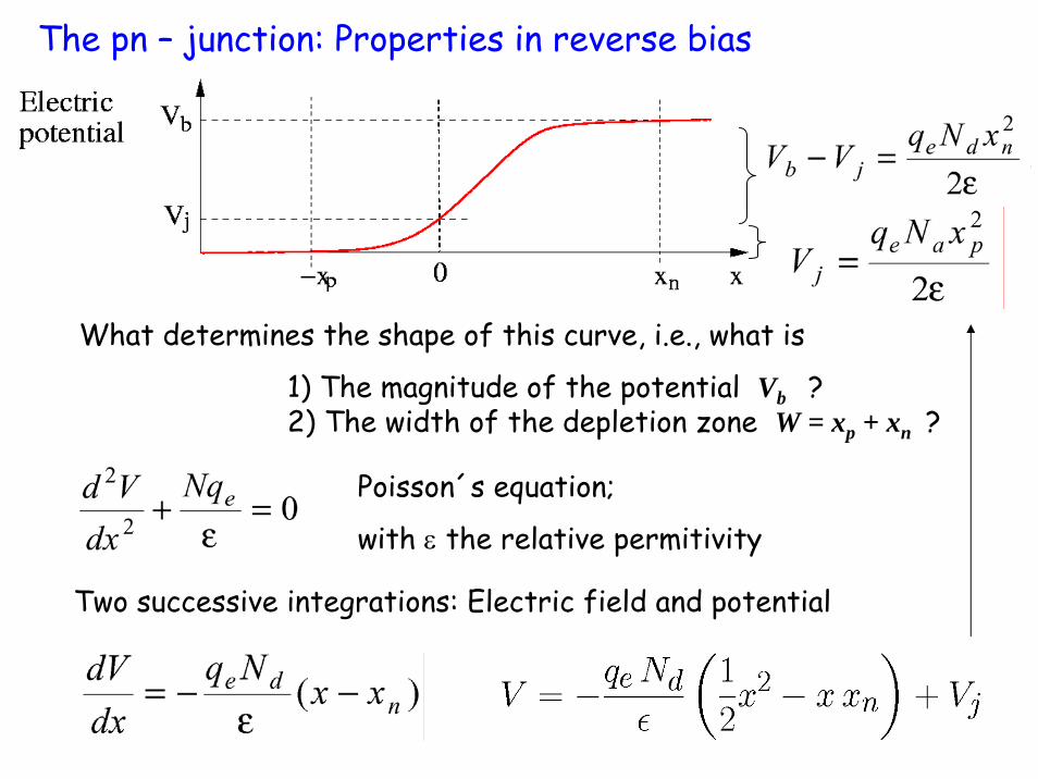
The pn – junction: Properties in reverse bias
What determines the shape of this curve, i.e., what is
1) The magnitude of the potential Vb ?2) The width of the depletion zone W = xp + xn ?
Poisson´s equation;
with ε the relative permitivity
Two successive integrations: Electric field and potential

Depletion width of the p-n junction in reverse bias
Bias voltage :
Charge neutrality :
Both equations can be solved for xp and x n resulting in the following expression for the depletion width :
If, for example, Na >> Nd, this expression simplifies to
Recommended