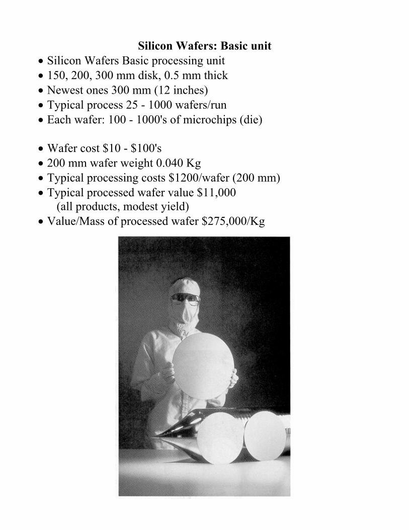
Silicon Wafers: Basic unit • Silicon Wafers Basic processing unit • 150, 200, 300 mm disk, 0.5 mm thick • Newest ones 300 mm (12 inches) • Typical process 25 - 1000 wafers/run • Each wafer: 100 - 1000's of microchips (die) • Wafer cost $10 - $100's • 200 mm wafer weight 0.040 Kg • Typical processing costs $1200/wafer (200 mm) • Typical processed wafer value $11,000 (all products, modest yield) • Value/Mass of processed wafer $275,000/Kg
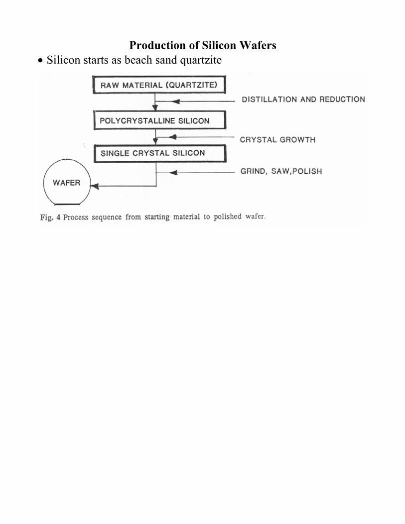
Production of Silicon Wafers • Silicon starts as beach sand quartzite
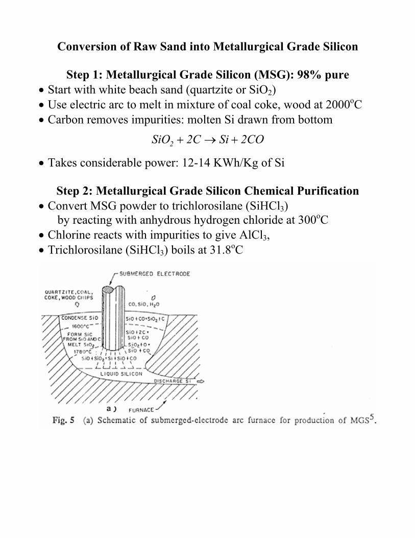
Conversion of Raw Sand into Metallurgical Grade Silicon
Step 1: Metallurgical Grade Silicon (MSG): 98% pure • Start with white beach sand (quartzite or SiO2) • Use electric arc to melt in mixture of coal coke, wood at 2000oC • Carbon removes impurities: molten Si drawn from bottom
CO2SiC2SiO2 +→+
• Takes considerable power: 12-14 KWh/Kg of Si
Step 2: Metallurgical Grade Silicon Chemical Purification • Convert MSG powder to trichlorosilane (SiHCl3) by reacting with anhydrous hydrogen chloride at 300oC • Chlorine reacts with impurities to give AlCl3, • Trichlorosilane (SiHCl3) boils at 31.8oC
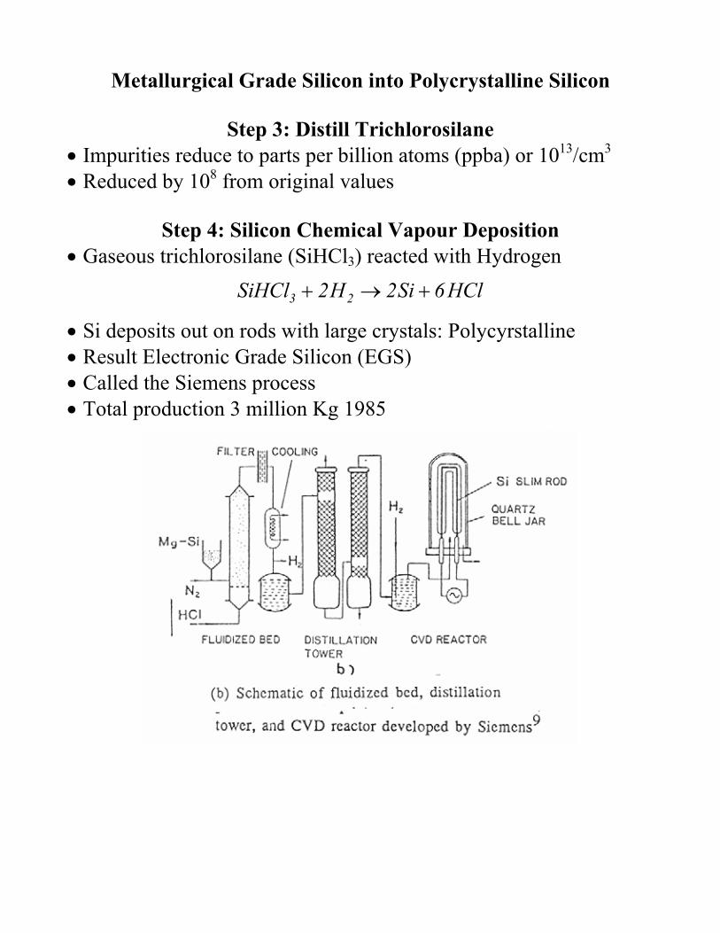
Metallurgical Grade Silicon into Polycrystalline Silicon
Step 3: Distill Trichlorosilane • Impurities reduce to parts per billion atoms (ppba) or 1013/cm3 • Reduced by 108 from original values
Step 4: Silicon Chemical Vapour Deposition • Gaseous trichlorosilane (SiHCl3) reacted with Hydrogen
HCl6Si2H2SiHCl 23 +→+
• Si deposits out on rods with large crystals: Polycyrstalline • Result Electronic Grade Silicon (EGS) • Called the Siemens process • Total production 3 million Kg 1985
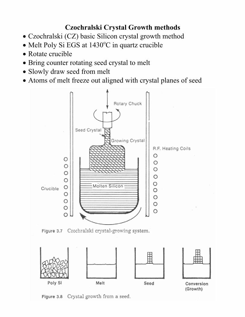
Czochralski Crystal Growth methods • Czochralski (CZ) basic Silicon crystal growth method • Melt Poly Si EGS at 1430oC in quartz crucible • Rotate crucible • Bring counter rotating seed crystal to melt • Slowly draw seed from melt • Atoms of melt freeze out aligned with crystal planes of seed
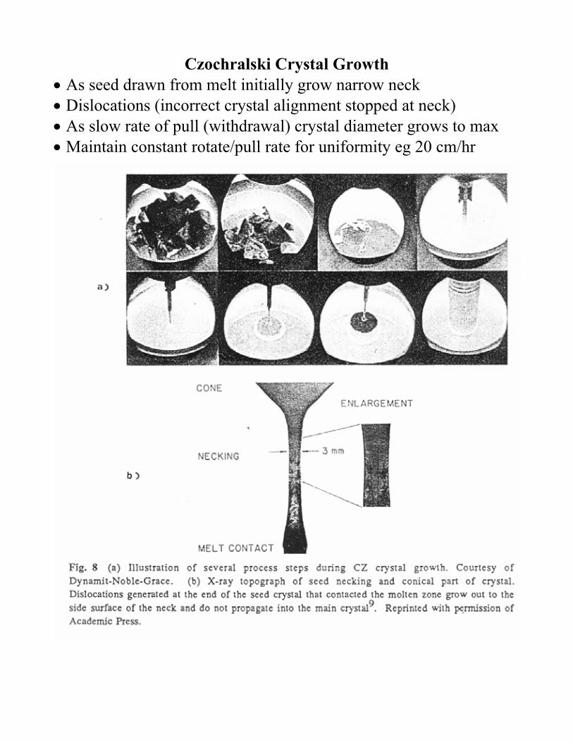
Czochralski Crystal Growth • As seed drawn from melt initially grow narrow neck • Dislocations (incorrect crystal alignment stopped at neck) • As slow rate of pull (withdrawal) crystal diameter grows to max • Maintain constant rotate/pull rate for uniformity eg 20 cm/hr
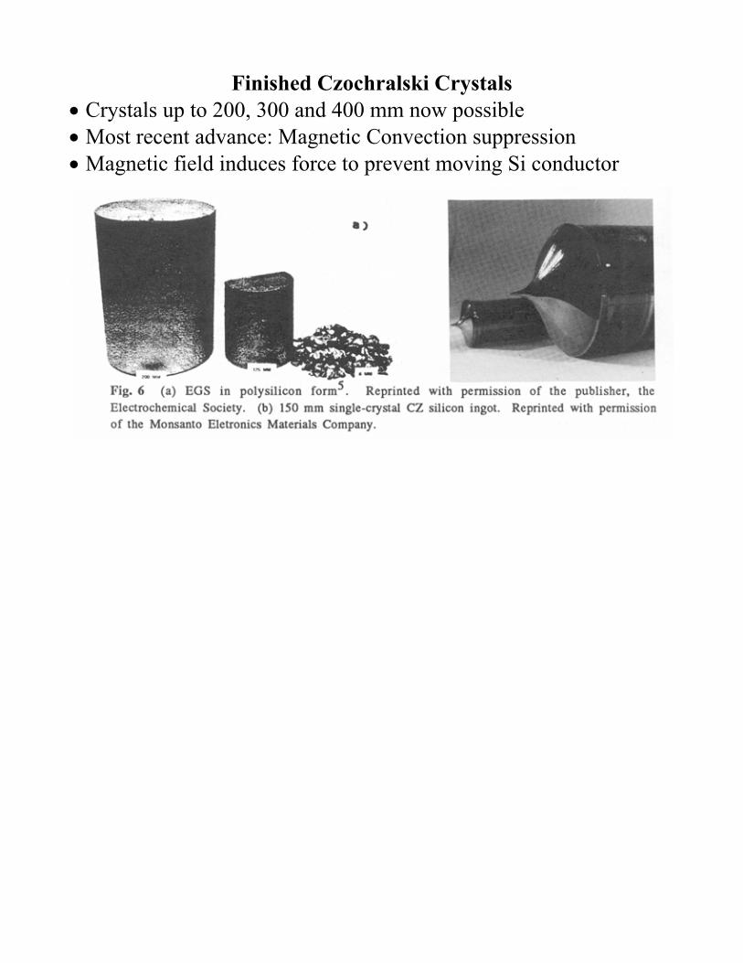
Finished Czochralski Crystals • Crystals up to 200, 300 and 400 mm now possible • Most recent advance: Magnetic Convection suppression • Magnetic field induces force to prevent moving Si conductor
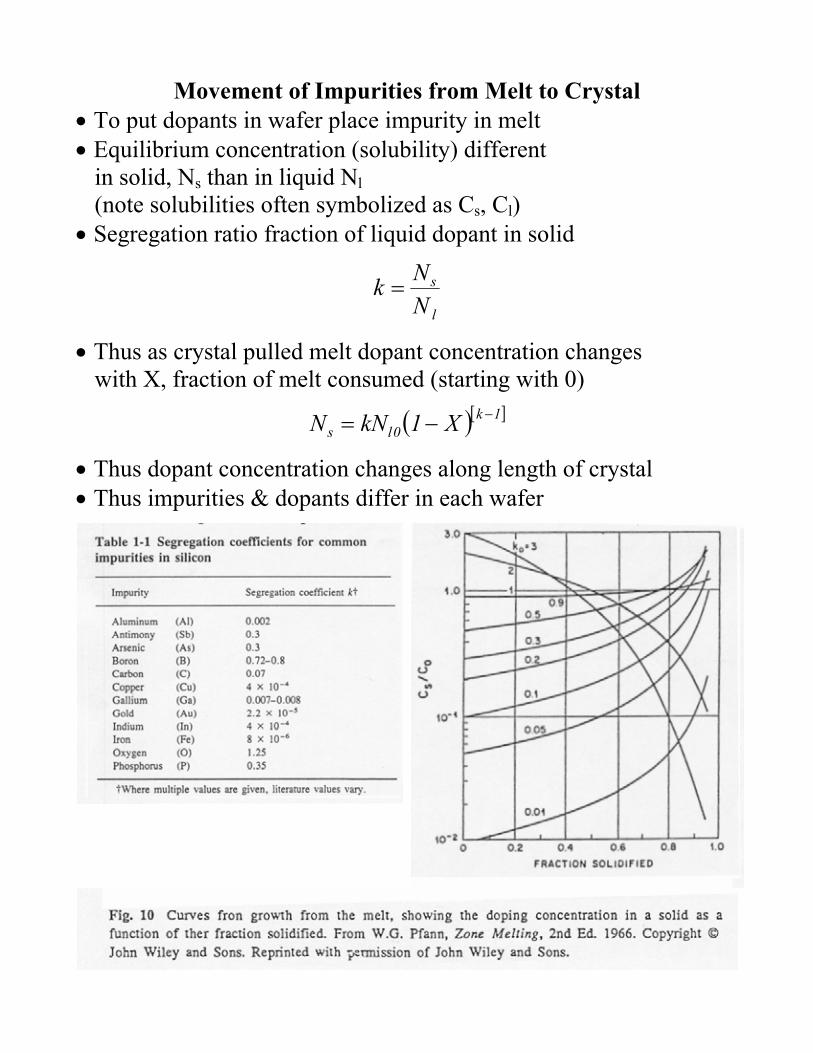
Movement of Impurities from Melt to Crystal • To put dopants in wafer place impurity in melt • Equilibrium concentration (solubility) different in solid, Ns than in liquid Nl (note solubilities often symbolized as Cs, Cl) • Segregation ratio fraction of liquid dopant in solid
l
s
NNk =
• Thus as crystal pulled melt dopant concentration changes with X, fraction of melt consumed (starting with 0)
( )[ ]1k0ls X1kNN −−=
• Thus dopant concentration changes along length of crystal • Thus impurities & dopants differ in each wafer
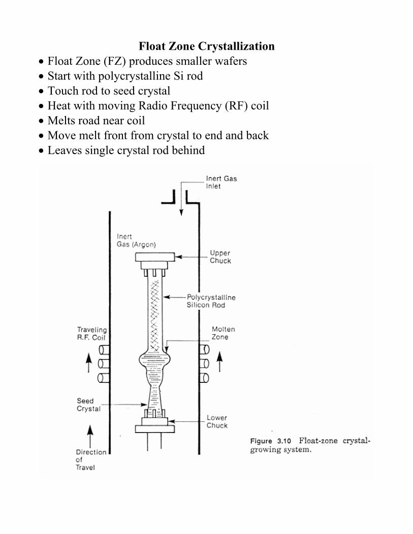
Float Zone Crystallization • Float Zone (FZ) produces smaller wafers • Start with polycrystalline Si rod • Touch rod to seed crystal • Heat with moving Radio Frequency (RF) coil • Melts road near coil • Move melt front from crystal to end and back • Leaves single crystal rod behind
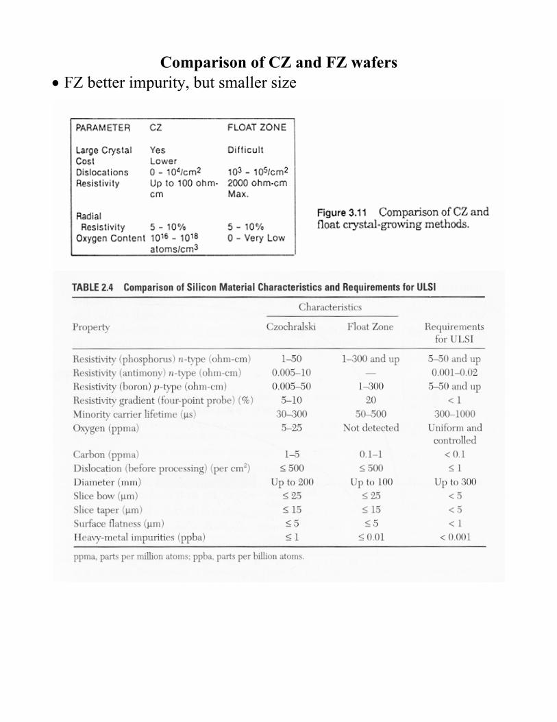
Comparison of CZ and FZ wafers • FZ better impurity, but smaller size
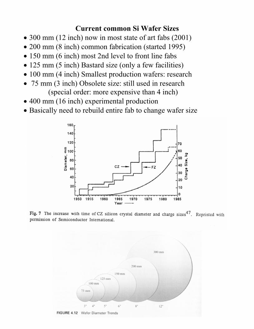
Current common Si Wafer Sizes • 300 mm (12 inch) now in most state of art fabs (2001) • 200 mm (8 inch) common fabrication (started 1995) • 150 mm (6 inch) most 2nd level to front line fabs • 125 mm (5 inch) Bastard size (only a few facilities) • 100 mm (4 inch) Smallest production wafers: research • 75 mm (3 inch) Obsolete size: still used in research (special order: more expensive than 4 inch) • 400 mm (16 inch) experimental production • Basically need to rebuild entire fab to change wafer size
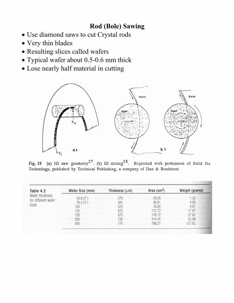
Rod (Bole) Sawing • Use diamond saws to cut Crystal rods • Very thin blades • Resulting slices called wafers • Typical wafer about 0.5-0.6 mm thick • Lose nearly half material in cutting
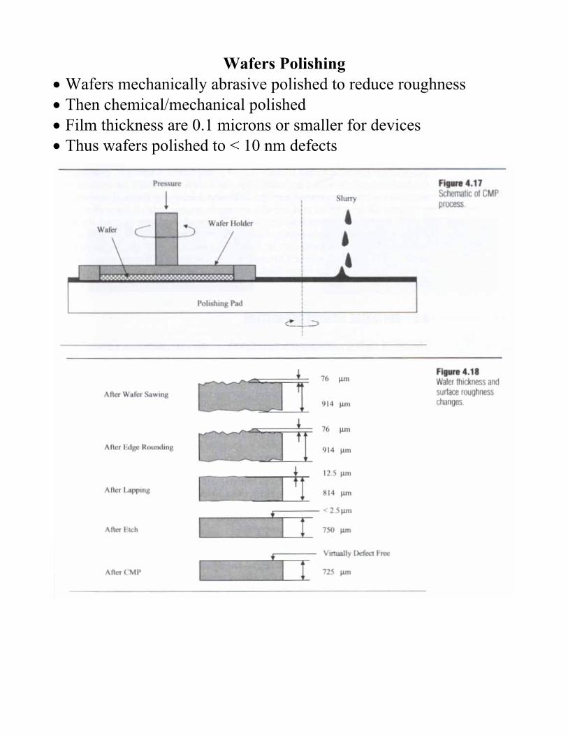
Wafers Polishing • Wafers mechanically abrasive polished to reduce roughness • Then chemical/mechanical polished • Film thickness are 0.1 microns or smaller for devices • Thus wafers polished to < 10 nm defects
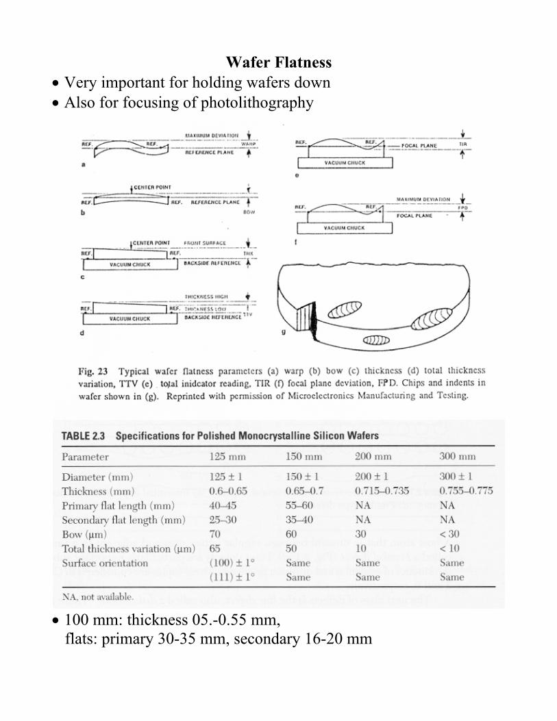
Wafer Flatness • Very important for holding wafers down • Also for focusing of photolithography
• 100 mm: thickness 05.-0.55 mm, flats: primary 30-35 mm, secondary 16-20 mm
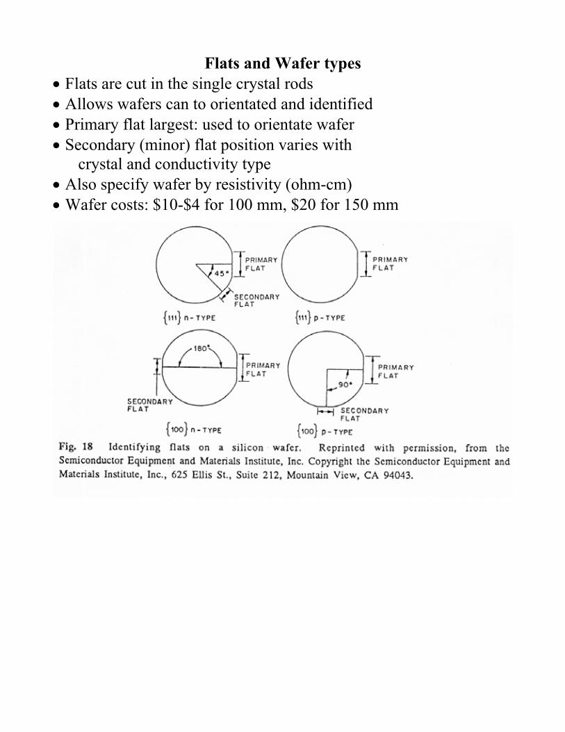
Flats and Wafer types • Flats are cut in the single crystal rods • Allows wafers can to orientated and identified • Primary flat largest: used to orientate wafer • Secondary (minor) flat position varies with crystal and conductivity type • Also specify wafer by resistivity (ohm-cm) • Wafer costs: $10-$4 for 100 mm, $20 for 150 mm
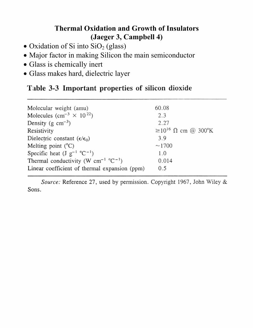
Thermal Oxidation and Growth of Insulators (Jaeger 3, Campbell 4)
• Oxidation of Si into SiO2 (glass) • Major factor in making Silicon the main semiconductor • Glass is chemically inert • Glass makes hard, dielectric layer
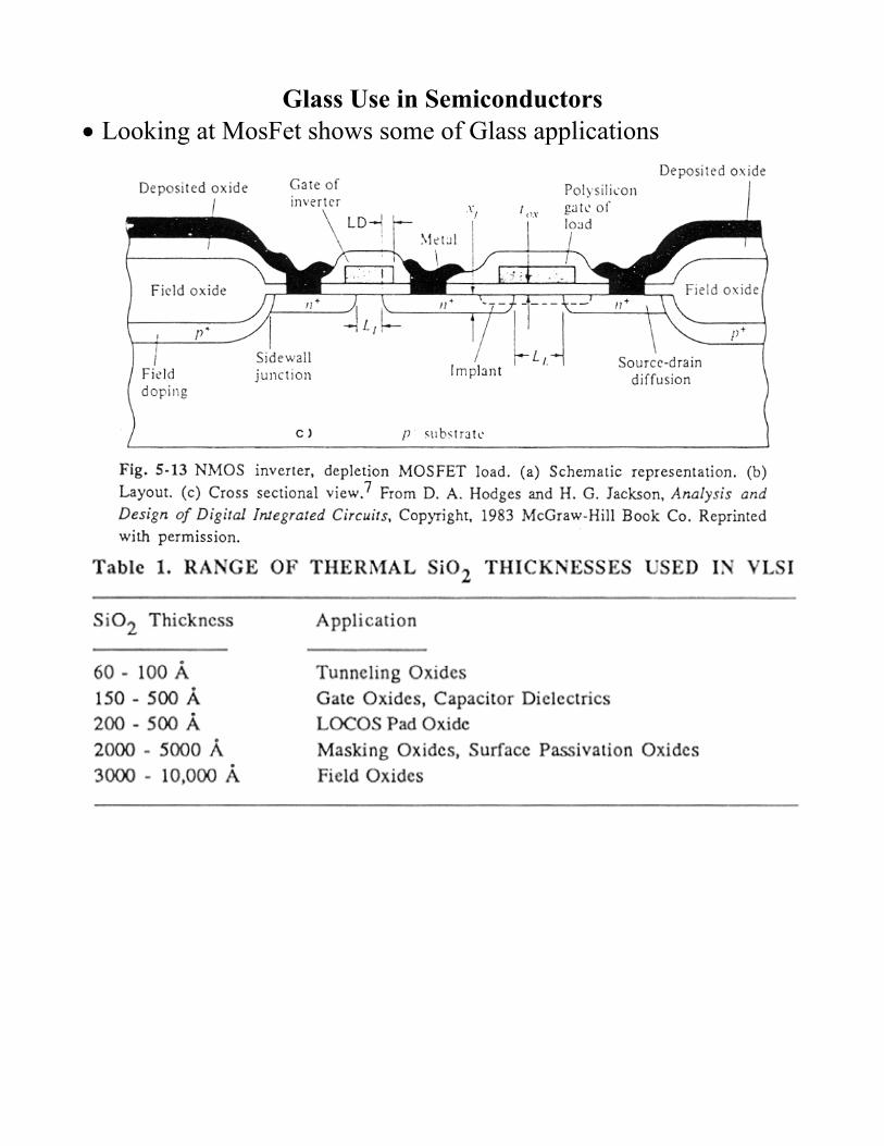
Glass Use in Semiconductors • Looking at MosFet shows some of Glass applications
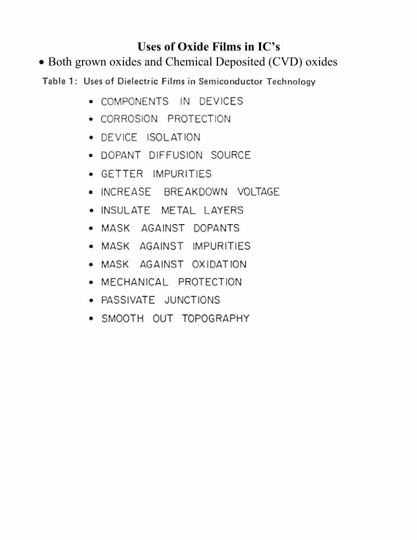
Uses of Oxide Films in IC’s • Both grown oxides and Chemical Deposited (CVD) oxides
Growth of Oxide Films • Done at high temperature in oxidizing gas • Thickness control and density determine process • Dry oxidation (denser oxides: gate oxide)
22 SiOOSi →+
• Wet Oxidation (lower density: Thick masking, Field oxides)
222 H2SiOOH2Si +→+ • Furnace growth charts depend on wet/dry and crystal orientation
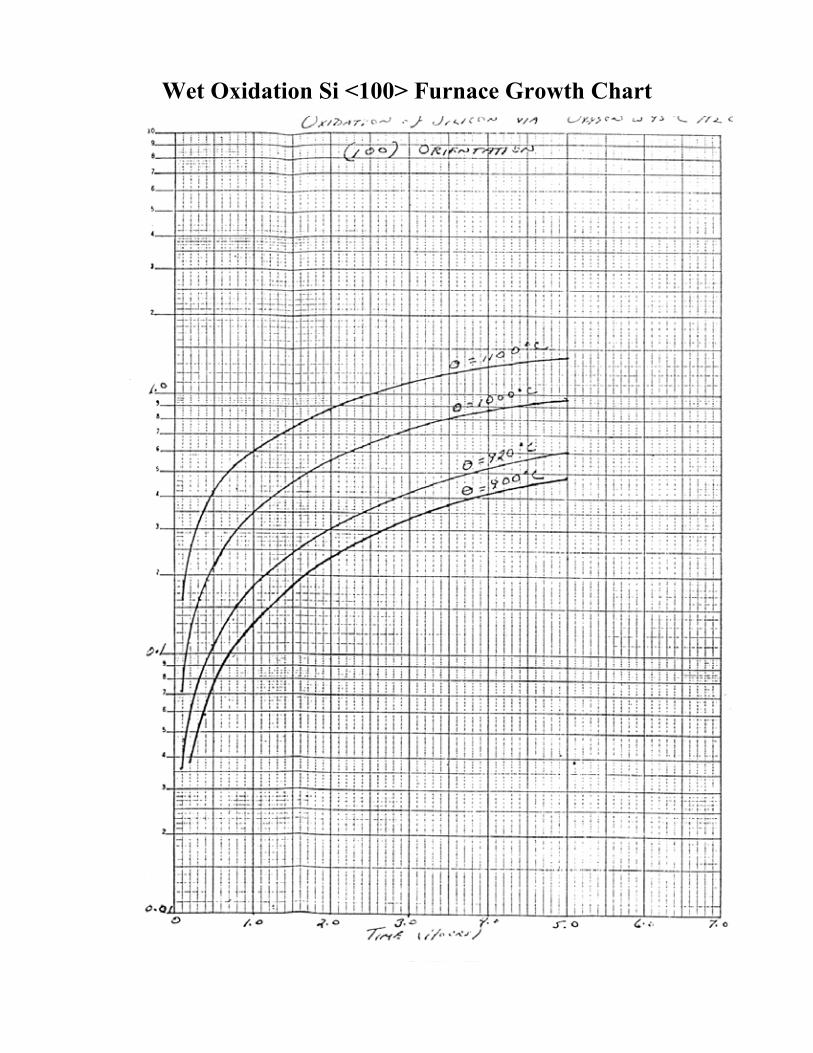
Wet Oxidation Si <100> Furnace Growth Chart
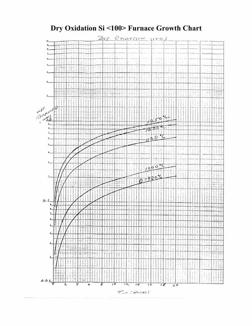
Dry Oxidation Si <100> Furnace Growth Chart
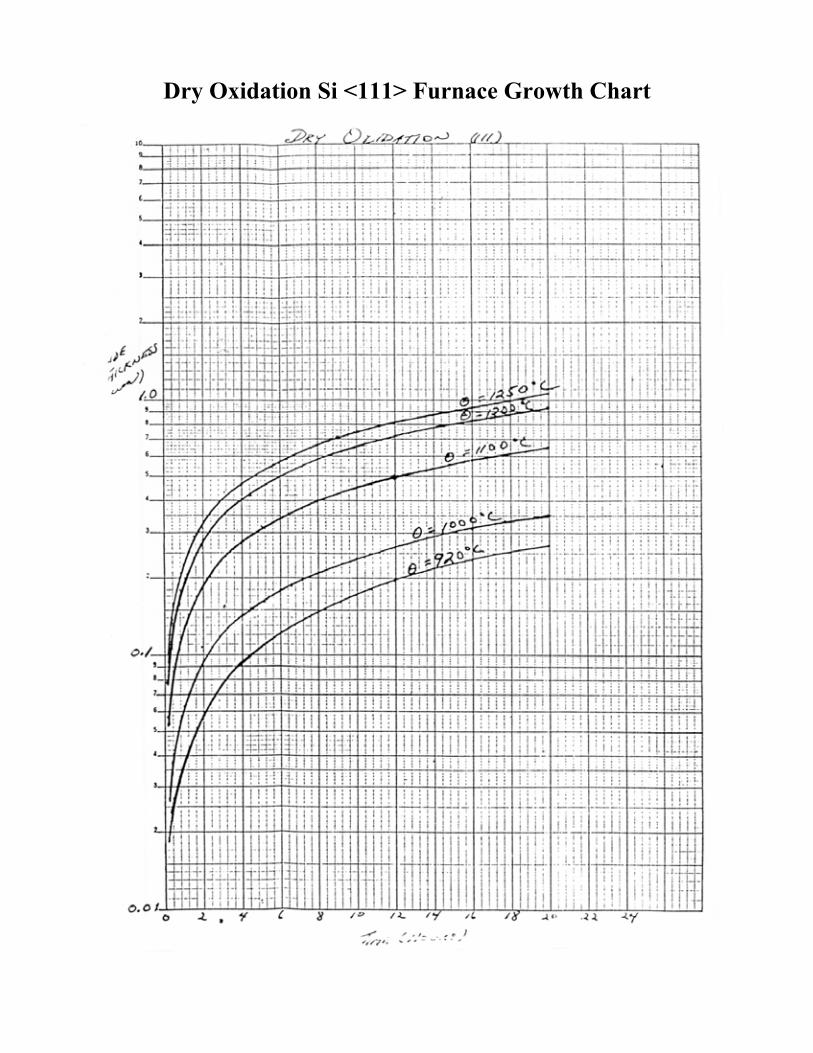
Dry Oxidation Si <111> Furnace Growth Chart
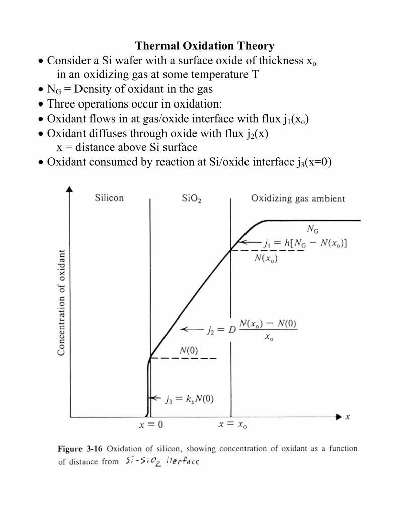
Thermal Oxidation Theory • Consider a Si wafer with a surface oxide of thickness xo in an oxidizing gas at some temperature T • NG = Density of oxidant in the gas • Three operations occur in oxidation: • Oxidant flows in at gas/oxide interface with flux j1(xo) • Oxidant diffuses through oxide with flux j2(x) x = distance above Si surface • Oxidant consumed by reaction at Si/oxide interface j3(x=0)
Thermal Oxidation Theory Flow at gas/SiO2 Surface: j1 • Flux is atoms/molecules passing given surface per unite time (unites atoms/cm2sec) • Oxidant declines from gas level NG to SiO2 surface due to flux into oxide • Flux flow a mass transport process • At oxide surface (x = x o) the flux into the oxide is
( )[ ]0G1 xNNhj −=
where h = mass transfer coefficient or proportionality constant N(xo) = oxidant concentration at SiO2 surface • h is related to diffusion of oxidant from gas to oxide and thickness of slow moving gas layer at surface Within oxide (0 << x << xo): j2 • Oxidant flow decreases linearly from the surface level
( ) ( ) ( )0
02 x
0NxNDxj −=
where D = Diffusion coefficient of oxidant in SiO2 N(0) = oxidant concentration at Si surface • Related to Fick's diffusion law
Reaction of Oxide at Si Surface: j3 • Reaction Rate of oxide in Si surface
( ) ( )0Nkxj s03 =
where ks = reaction rate constant Relating Flux at Interfaces • Oxidant is consumed only at Si: Thus under steady state
321 jjj ==
• Thus solving for the oxidant concentration at 0 and xo
( )
Dxk
hk1
N0N0ss
G
++=
( )
Dxk
hk1
Dxk1N
xN0ss
0sG
0++
+
=
• Growth of oxide thickness is related to reaction rate by
( )γ0Nk
dtdx s0 =
where γ = no. of oxidant molecules used per unite oxide volume γ = 2.2x1022 cm-2 for O2 (Dry oxidation) γ = 4.4x1022 cm-2 for H2O (Wet oxidation)
Thermal Oxidation Solutions: Grove's Law • Combining this with N(0) formula
Dxk
hk1
Nkdtdx
0ss
Gs0
++=γ
• Deal and Grove (1965) solved this assuming xo(t=0) = xi
( )τ+=+ tBAxx 020
with
+=h1
k1D2As
γGDN2B =
BAxx i
2i +=τ
• Thus start with film xi which is defined to have taken time τ and grow for additional time t2 then get film
( ) ( )τ+= 20 tx0x
• ie: Result same as growing the film continuously for time t = t2 + τ
• Does not matter which oxidation process used for xi time used is calculated for the process of the new growth not for process used to actually grow oxide • Then solve the quadratic equation for x0, using A, B & τ
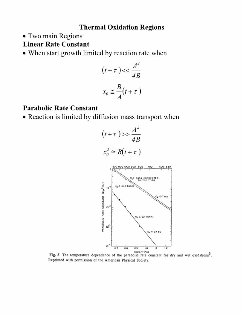
Thermal Oxidation Regions • Two main Regions Linear Rate Constant • When start growth limited by reaction rate when
( )B4At2
<<+τ
( )τ+≅ tABx0
Parabolic Rate Constant • Reaction is limited by diffusion mass transport when
( )B4At2
>>+τ
( )τ+≅ tBx20
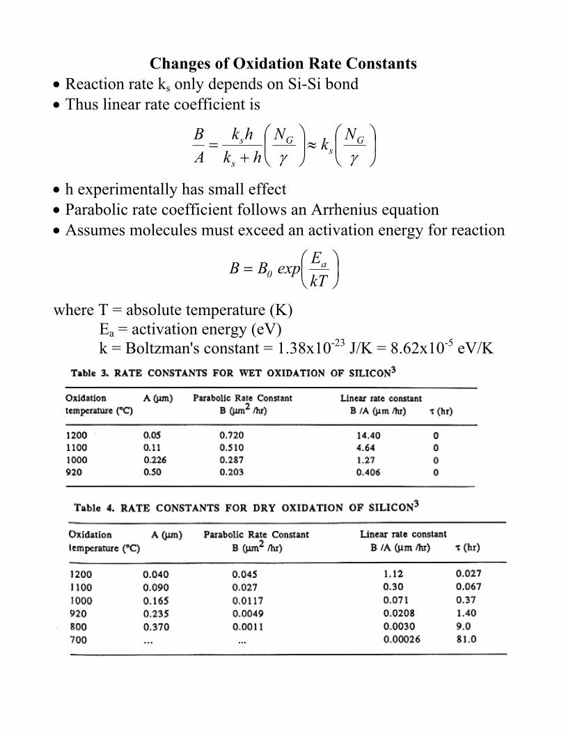
Changes of Oxidation Rate Constants • Reaction rate ks only depends on Si-Si bond • Thus linear rate coefficient is
≈
+
=γγG
sG
s
s NkNhkhk
AB
• h experimentally has small effect • Parabolic rate coefficient follows an Arrhenius equation • Assumes molecules must exceed an activation energy for reaction
=kTEexpBB a
0
where T = absolute temperature (K) Ea = activation energy (eV) k = Boltzman's constant = 1.38x10⁻²³ J/K = 8.62x10⁻⁵ eV/K
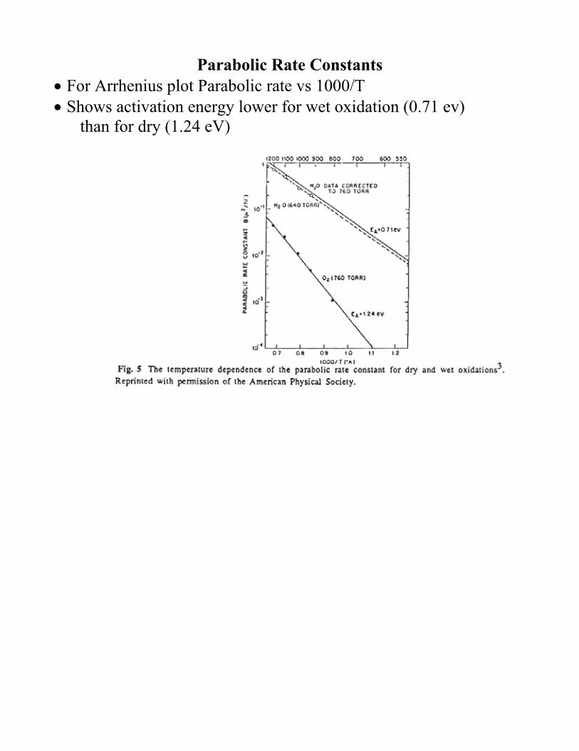
Parabolic Rate Constants • For Arrhenius plot Parabolic rate vs 1000/T • Shows activation energy lower for wet oxidation (0.71 ev) than for dry (1.24 eV)
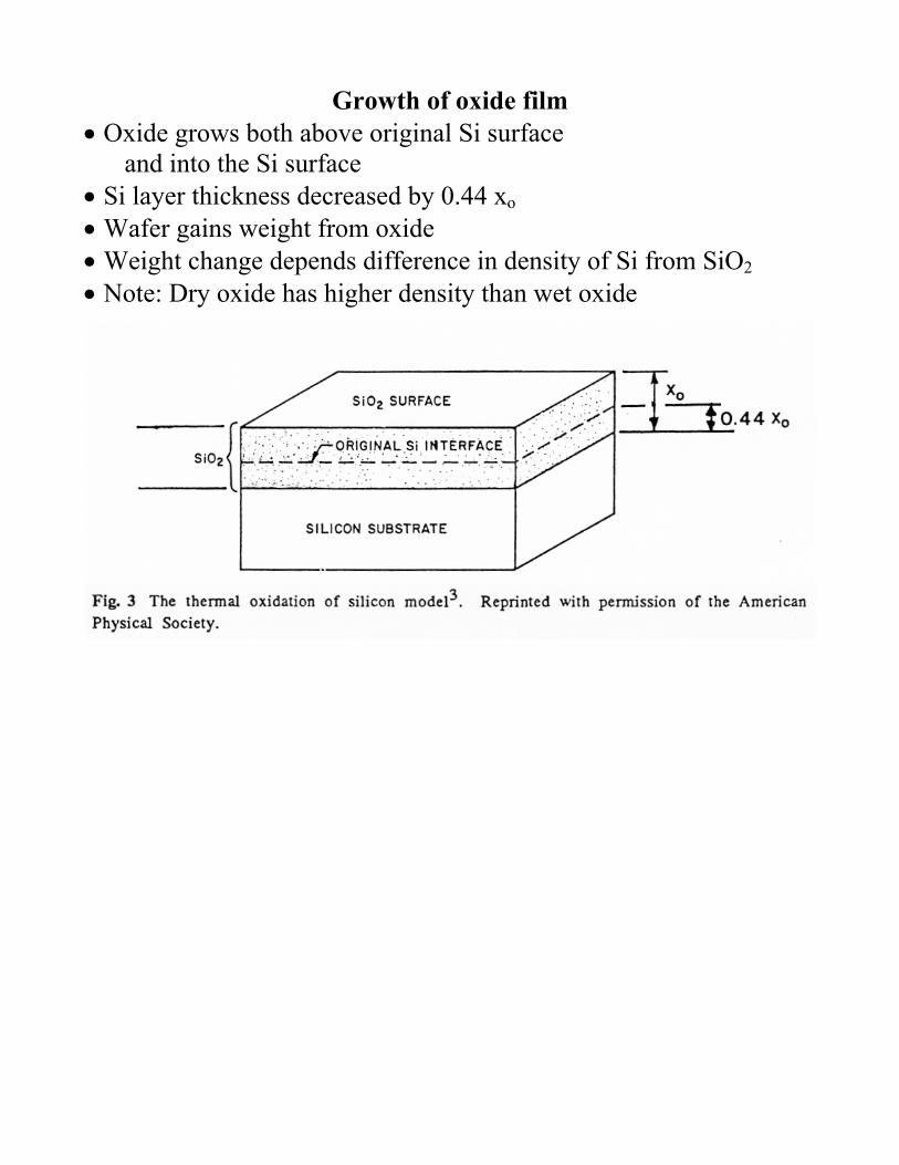
Growth of oxide film • Oxide grows both above original Si surface and into the Si surface • Si layer thickness decreased by 0.44 xo • Wafer gains weight from oxide • Weight change depends difference in density of Si from SiO2 • Note: Dry oxide has higher density than wet oxide
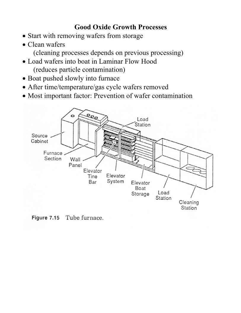
Good Oxide Growth Processes • Start with removing wafers from storage • Clean wafers (cleaning processes depends on previous processing) • Load wafers into boat in Laminar Flow Hood (reduces particle contamination) • Boat pushed slowly into furnace • After time/temperature/gas cycle wafers removed • Most important factor: Prevention of wafer contamination
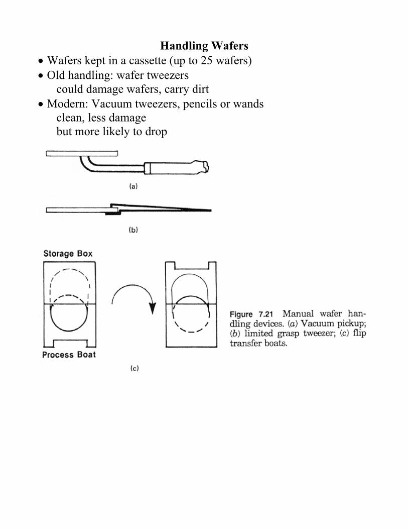
Handling Wafers • Wafers kept in a cassette (up to 25 wafers) • Old handling: wafer tweezers could damage wafers, carry dirt • Modern: Vacuum tweezers, pencils or wands clean, less damage but more likely to drop
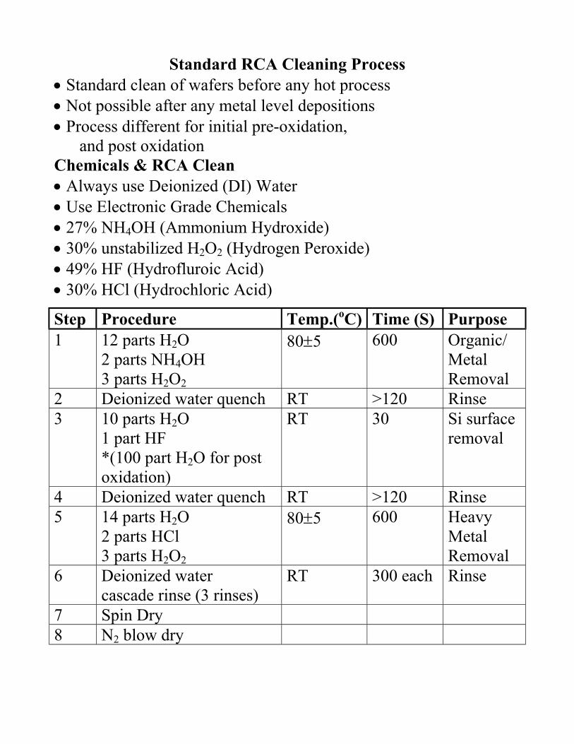
Standard RCA Cleaning Process • Standard clean of wafers before any hot process • Not possible after any metal level depositions • Process different for initial pre-oxidation, and post oxidation Chemicals & RCA Clean • Always use Deionized (DI) Water • Use Electronic Grade Chemicals • 27% NH4OH (Ammonium Hydroxide) • 30% unstabilized H2O2 (Hydrogen Peroxide) • 49% HF (Hydrofluroic Acid) • 30% HCl (Hydrochloric Acid)
Step Procedure Temp.(oC) Time (S) Purpose 1 12 parts H2O
2 parts NH4OH 3 parts H2O2
80±5 600 Organic/ Metal Removal
2 Deionized water quench RT >120 Rinse 3 10 parts H2O
1 part HF *(100 part H2O for post oxidation)
RT 30 Si surface removal
4 Deionized water quench RT >120 Rinse 5 14 parts H2O
2 parts HCl 3 parts H2O2
80±5 600 Heavy Metal Removal
6 Deionized water cascade rinse (3 rinses)
RT 300 each Rinse
7 Spin Dry 8 N2 blow dry
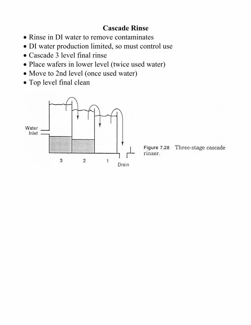
Cascade Rinse • Rinse in DI water to remove contaminates • DI water production limited, so must control use • Cascade 3 level final rinse • Place wafers in lower level (twice used water) • Move to 2nd level (once used water) • Top level final clean
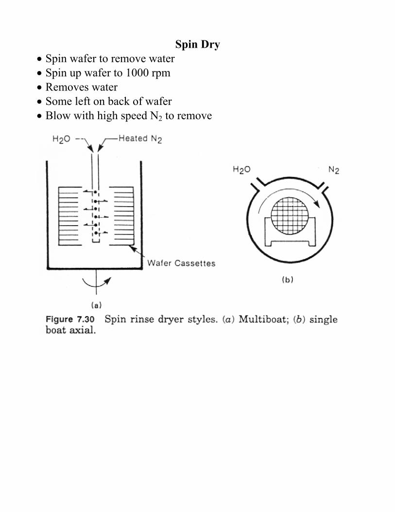
Spin Dry • Spin wafer to remove water • Spin up wafer to 1000 rpm • Removes water • Some left on back of wafer • Blow with high speed N2 to remove
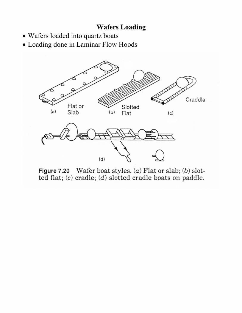
Wafers Loading • Wafers loaded into quartz boats • Loading done in Laminar Flow Hoods
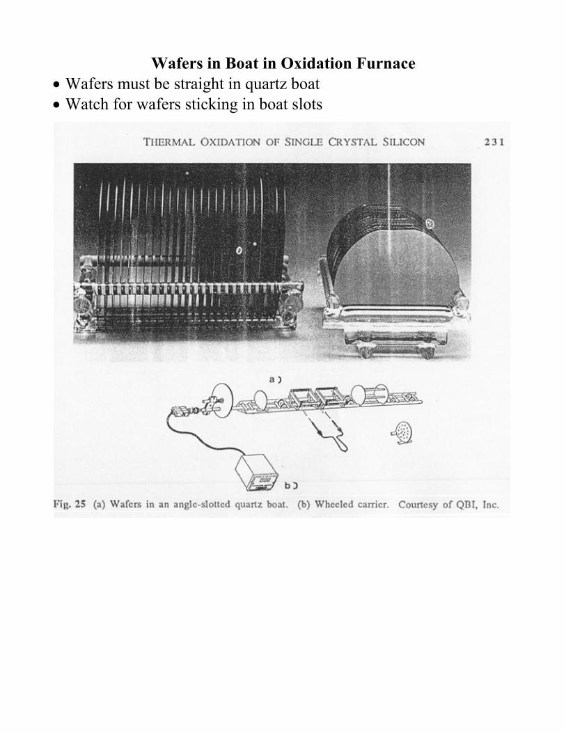
Wafers in Boat in Oxidation Furnace • Wafers must be straight in quartz boat • Watch for wafers sticking in boat slots
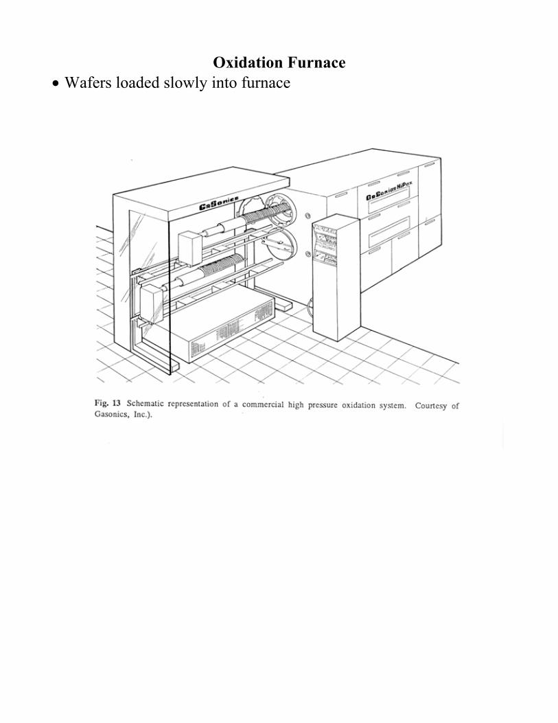
Oxidation Furnace • Wafers loaded slowly into furnace
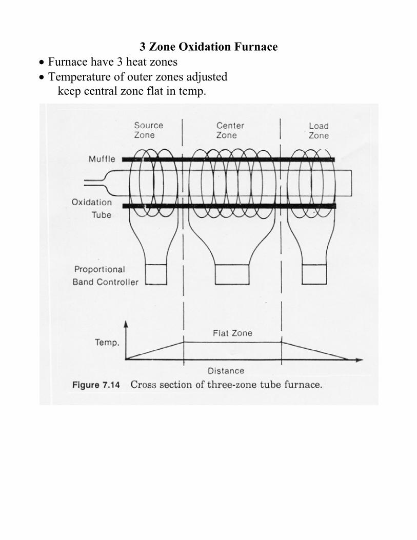
3 Zone Oxidation Furnace • Furnace have 3 heat zones • Temperature of outer zones adjusted keep central zone flat in temp.
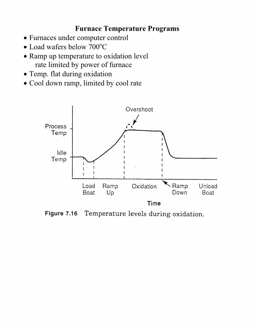
Furnace Temperature Programs • Furnaces under computer control • Load wafers below 700oC • Ramp up temperature to oxidation level rate limited by power of furnace • Temp. flat during oxidation • Cool down ramp, limited by cool rate
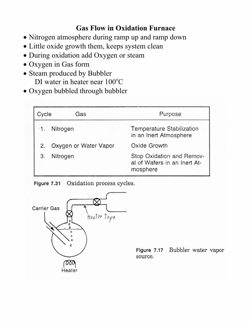
Gas Flow in Oxidation Furnace • Nitrogen atmosphere during ramp up and ramp down • Little oxide growth them, keeps system clean • During oxidation add Oxygen or steam • Oxygen in Gas form • Steam produced by Bubbler DI water in heater near 100oC • Oxygen bubbled through bubbler
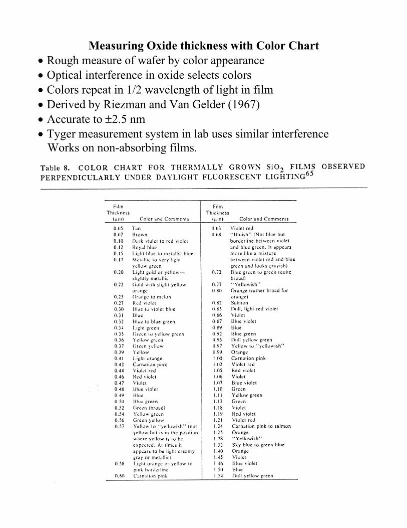
Measuring Oxide thickness with Color Chart • Rough measure of wafer by color appearance • Optical interference in oxide selects colors • Colors repeat in 1/2 wavelength of light in film • Derived by Riezman and Van Gelder (1967) • Accurate to ±2.5 nm • Tyger measurement system in lab uses similar interference Works on non-absorbing films.
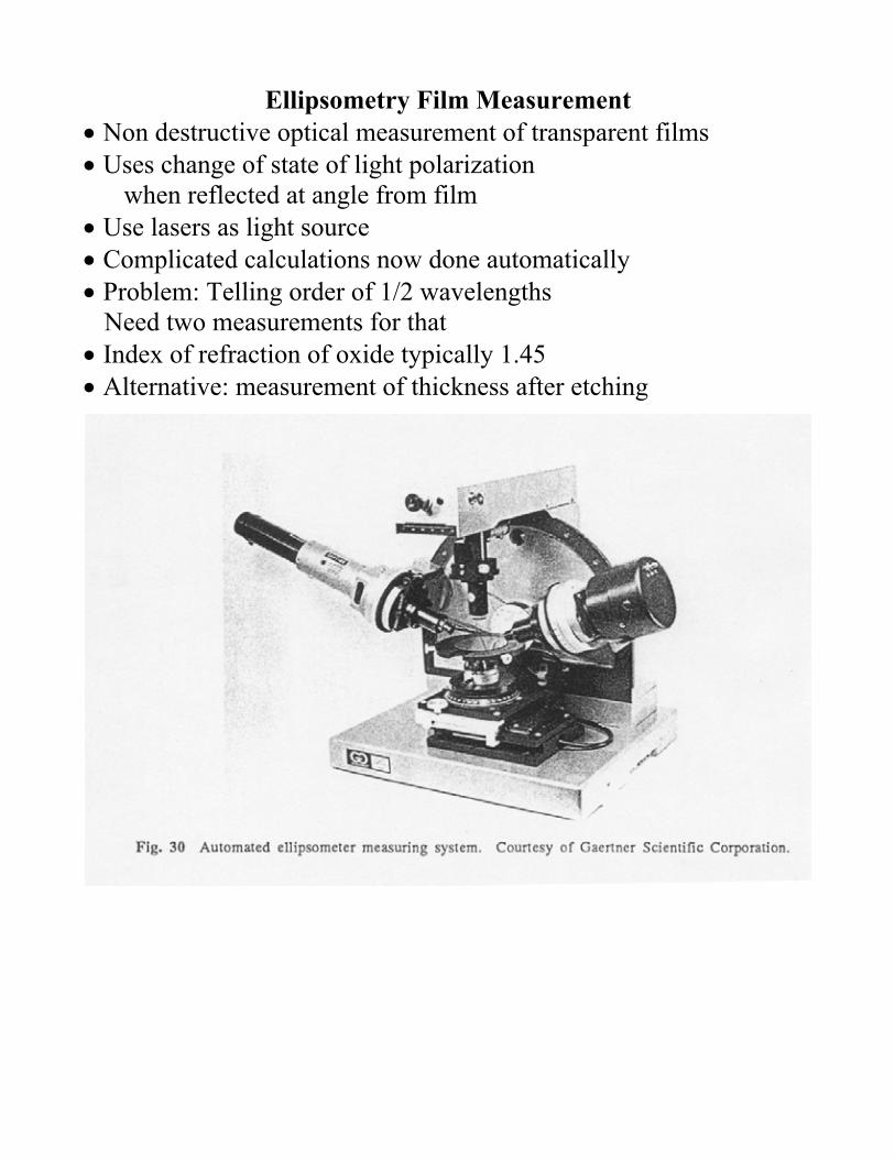
Ellipsometry Film Measurement • Non destructive optical measurement of transparent films • Uses change of state of light polarization when reflected at angle from film • Use lasers as light source • Complicated calculations now done automatically • Problem: Telling order of 1/2 wavelengths Need two measurements for that • Index of refraction of oxide typically 1.45 • Alternative: measurement of thickness after etching
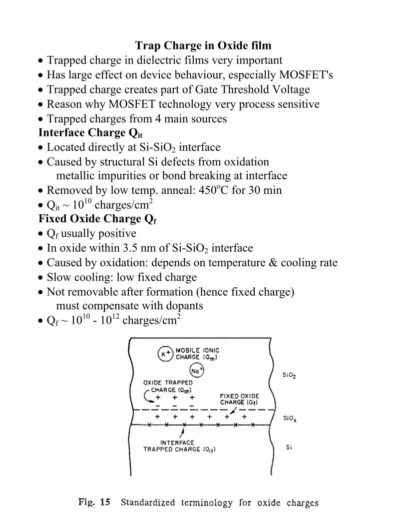
Trap Charge in Oxide film • Trapped charge in dielectric films very important • Has large effect on device behaviour, especially MOSFET's • Trapped charge creates part of Gate Threshold Voltage • Reason why MOSFET technology very process sensitive • Trapped charges from 4 main sources Interface Charge Qit • Located directly at Si-SiO2 interface • Caused by structural Si defects from oxidation metallic impurities or bond breaking at interface • Removed by low temp. anneal: 450oC for 30 min • Qit ~ 1010 charges/cm2 Fixed Oxide Charge Qf • Qf usually positive • In oxide within 3.5 nm of Si-SiO2 interface • Caused by oxidation: depends on temperature & cooling rate • Slow cooling: low fixed charge • Not removable after formation (hence fixed charge) must compensate with dopants • Qf ~ 1010 - 1012 charges/cm2
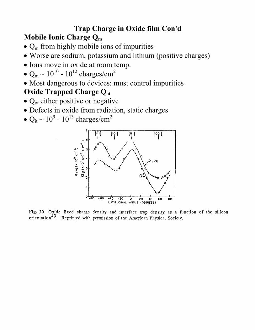
Trap Charge in Oxide film Con'd Mobile Ionic Charge Qm • Qm from highly mobile ions of impurities • Worse are sodium, potassium and lithium (positive charges) • Ions move in oxide at room temp. • Qm ~ 1010 - 1012 charges/cm2 • Most dangerous to devices: must control impurities Oxide Trapped Charge Qot • Qot either positive or negative • Defects in oxide from radiation, static charges • Qit ~ 109 - 1013 charges/cm2
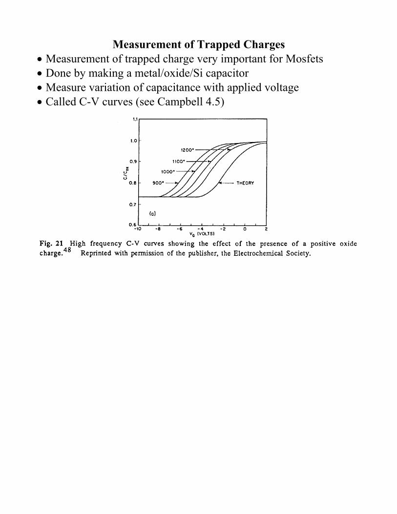
Measurement of Trapped Charges • Measurement of trapped charge very important for Mosfets • Done by making a metal/oxide/Si capacitor • Measure variation of capacitance with applied voltage • Called C-V curves (see Campbell 4.5)
Recommended