Embed Size (px)
Citation preview

Silicon Wafers: Basic unit Silicon Wafers Basic processing unit 100, 150, 200, 300 mm disk, 0.5-0.8 mm thick Current industrial standard 300 mm (12 inches) Most research labs 100, 150 mm wafers (ours 100) Typical process 25 - 1000 wafers/run Each wafer: 100 - 1000's of microchips (die) Wafer cost $10 - $100's 200 mm wafer weight 0.040 Kg Typical processing costs $1200/wafer (200 mm) Typical processed wafer value $11,000 (all products, modest yield) Value/Mass of processed wafer $275,000/Kg
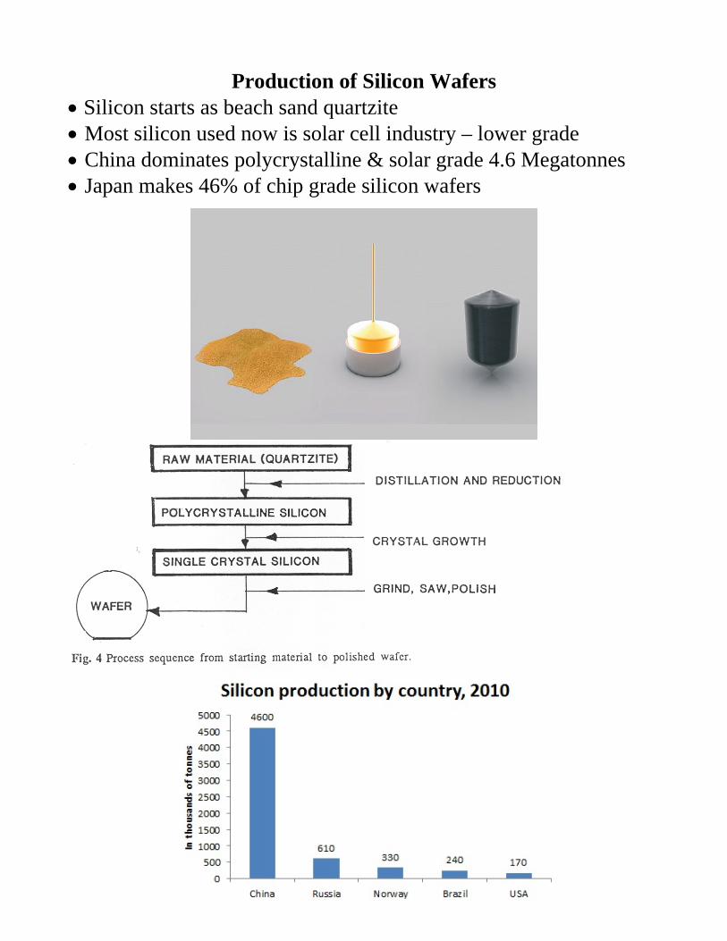
Production of Silicon Wafers Silicon starts as beach sand quartzite Most silicon used now is solar cell industry – lower grade China dominates polycrystalline & solar grade 4.6 Megatonnes Japan makes 46% of chip grade silicon wafers
Conversion of Raw Sand into Metallurgical Grade Silicon
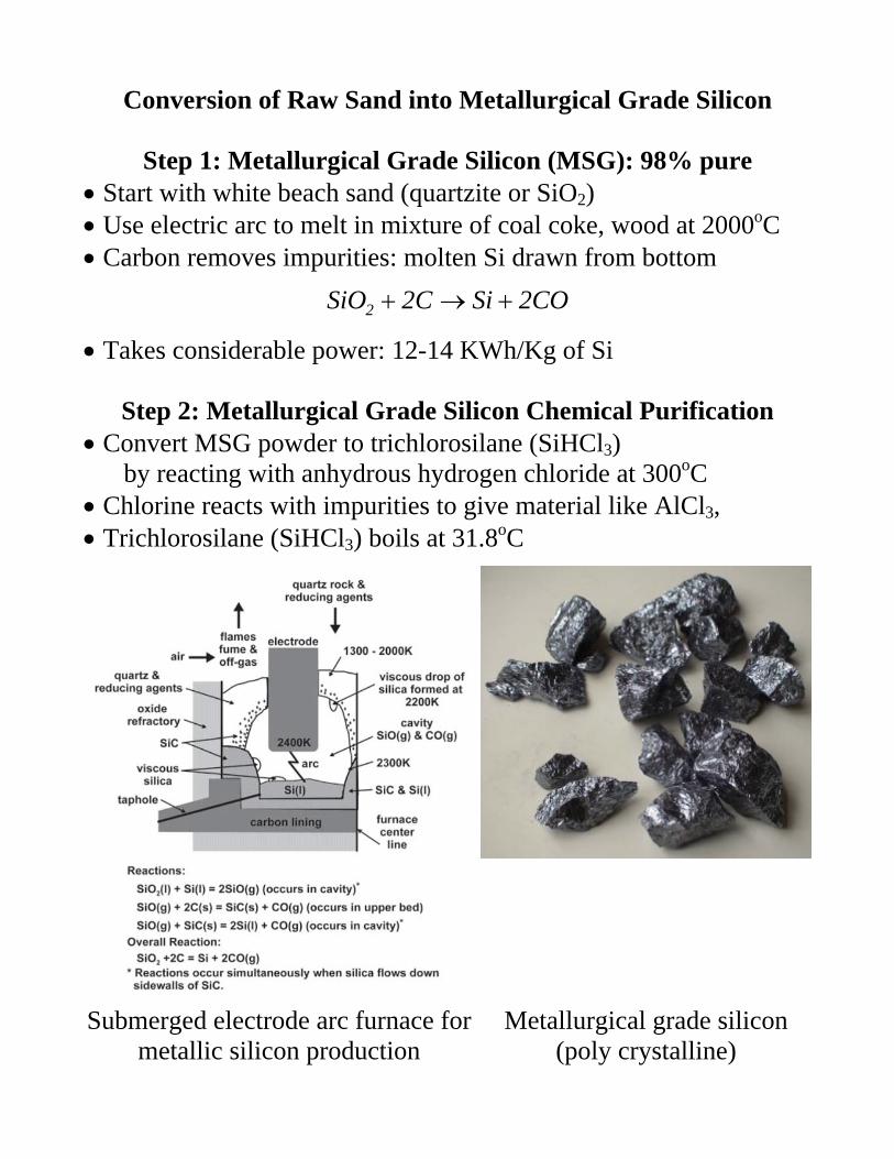
Step 1: Metallurgical Grade Silicon (MSG): 98% pure Start with white beach sand (quartzite or SiO2) Use electric arc to melt in mixture of coal coke, wood at 2000oC Carbon removes impurities: molten Si drawn from bottom
CO2SiC2SiO2
Takes considerable power: 12-14 KWh/Kg of Si
Step 2: Metallurgical Grade Silicon Chemical Purification Convert MSG powder to trichlorosilane (SiHCl3) by reacting with anhydrous hydrogen chloride at 300oC Chlorine reacts with impurities to give material like AlCl3, Trichlorosilane (SiHCl3) boils at 31.8oC
Submerged electrode arc furnace for metallic silicon production
Metallurgical grade silicon (poly crystalline)
Metallurgical Grade Silicon into Polycrystalline Silicon
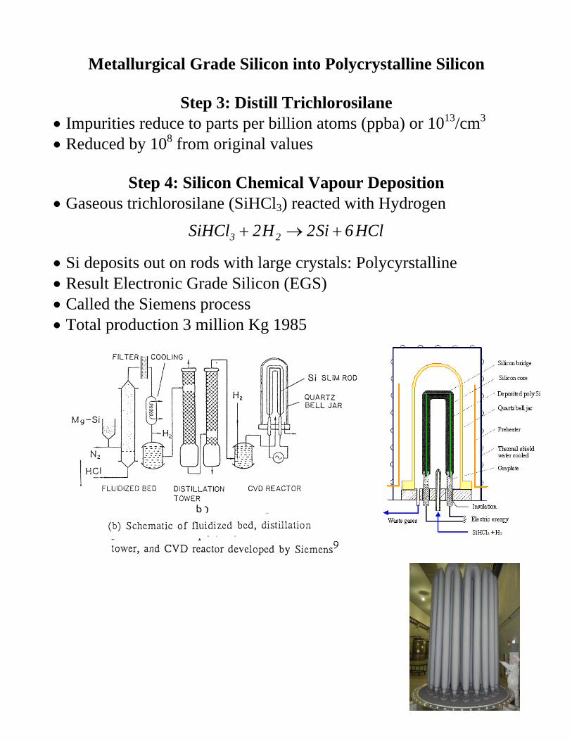
Step 3: Distill Trichlorosilane Impurities reduce to parts per billion atoms (ppba) or 1013/cm3 Reduced by 108 from original values
Step 4: Silicon Chemical Vapour Deposition Gaseous trichlorosilane (SiHCl3) reacted with Hydrogen
HCl6Si2H2SiHCl 23
Si deposits out on rods with large crystals: Polycyrstalline Result Electronic Grade Silicon (EGS) Called the Siemens process Total production 3 million Kg 1985
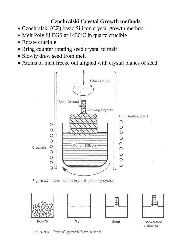
Czochralski Crystal Growth methods Czochralski (CZ) basic Silicon crystal growth method Melt Poly Si EGS at 1430oC in quartz crucible Rotate crucible Bring counter rotating seed crystal to melt Slowly draw seed from melt Atoms of melt freeze out aligned with crystal planes of seed
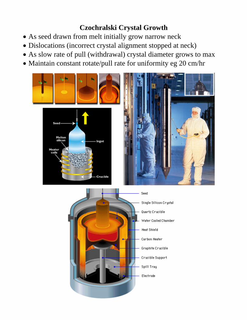
Czochralski Crystal Growth As seed drawn from melt initially grow narrow neck Dislocations (incorrect crystal alignment stopped at neck) As slow rate of pull (withdrawal) crystal diameter grows to max Maintain constant rotate/pull rate for uniformity eg 20 cm/hr
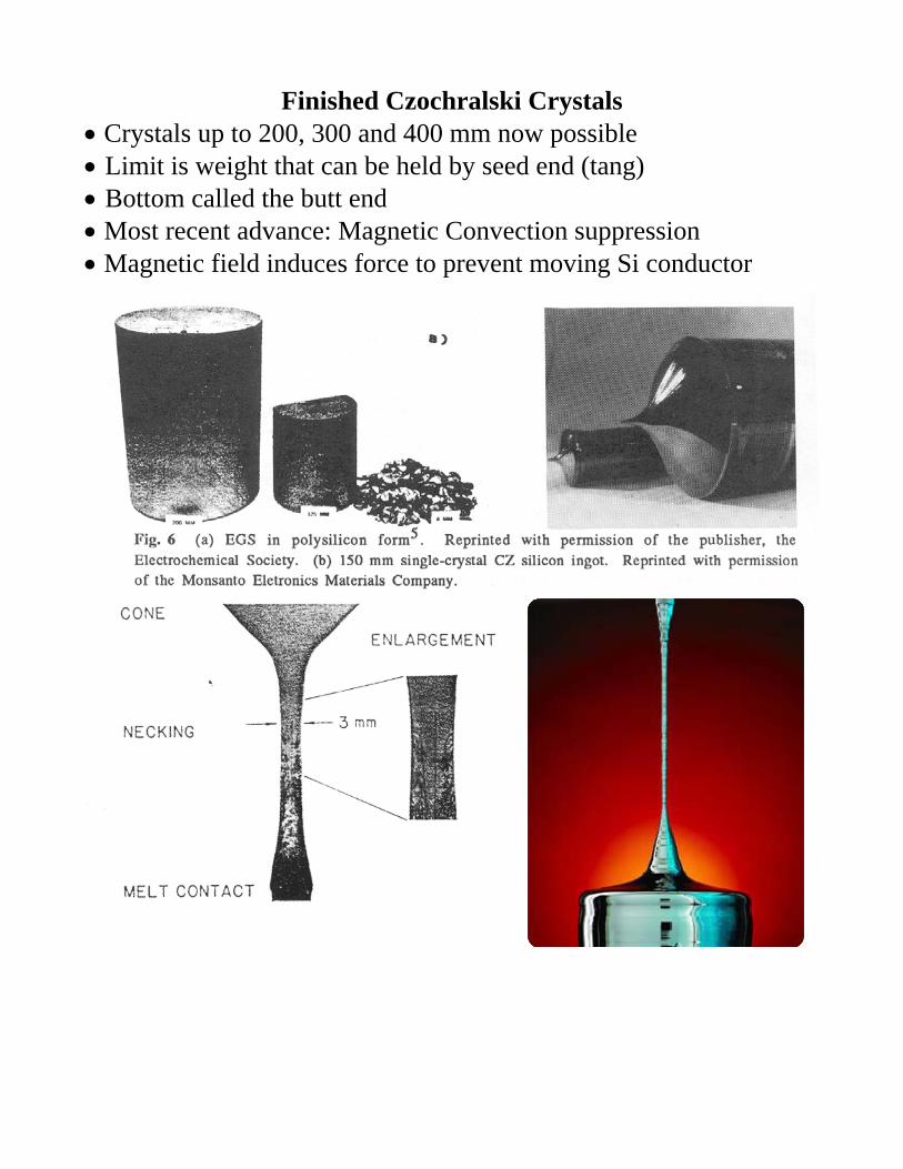
Finished Czochralski Crystals Crystals up to 200, 300 and 400 mm now possible Limit is weight that can be held by seed end (tang) Bottom called the butt end Most recent advance: Magnetic Convection suppression Magnetic field induces force to prevent moving Si conductor
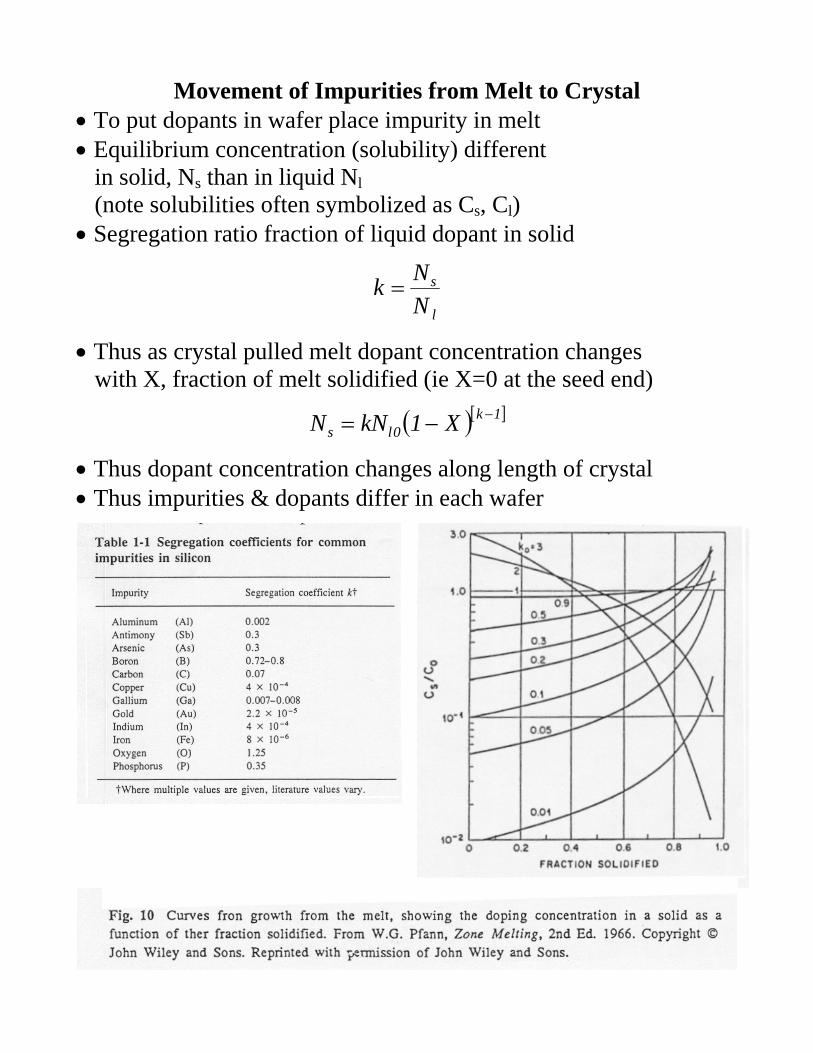
Movement of Impurities from Melt to Crystal To put dopants in wafer place impurity in melt Equilibrium concentration (solubility) different in solid, Ns than in liquid Nl (note solubilities often symbolized as Cs, Cl) Segregation ratio fraction of liquid dopant in solid
l
s
N
Nk
Thus as crystal pulled melt dopant concentration changes with X, fraction of melt solidified (ie X=0 at the seed end)
1k0ls X1kNN
Thus dopant concentration changes along length of crystal Thus impurities & dopants differ in each wafer
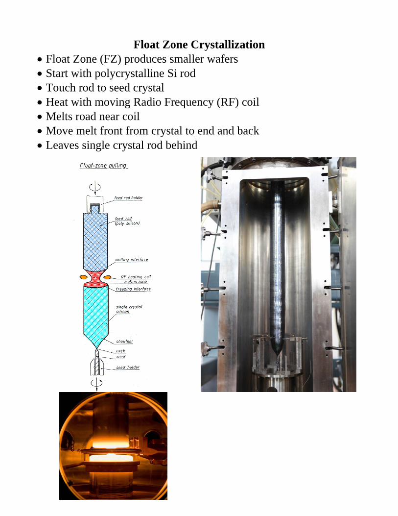
Float Zone Crystallization Float Zone (FZ) produces smaller wafers Start with polycrystalline Si rod Touch rod to seed crystal Heat with moving Radio Frequency (RF) coil Melts road near coil Move melt front from crystal to end and back Leaves single crystal rod behind
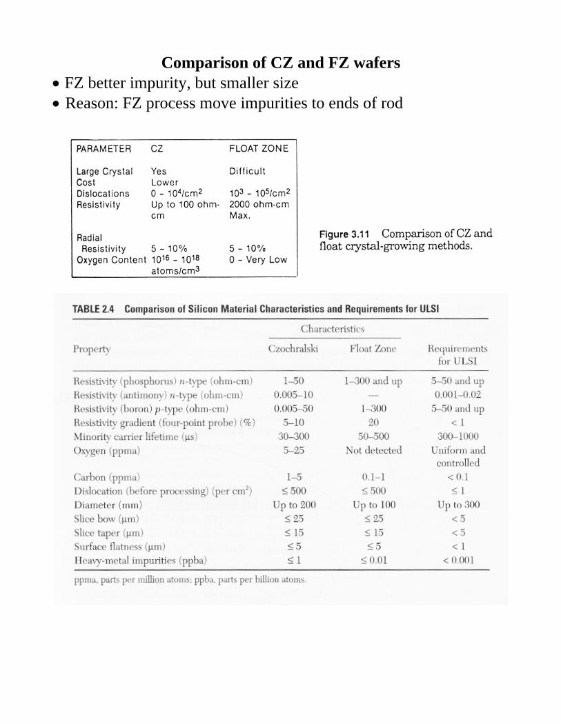
Comparison of CZ and FZ wafers FZ better impurity, but smaller size Reason: FZ process move impurities to ends of rod
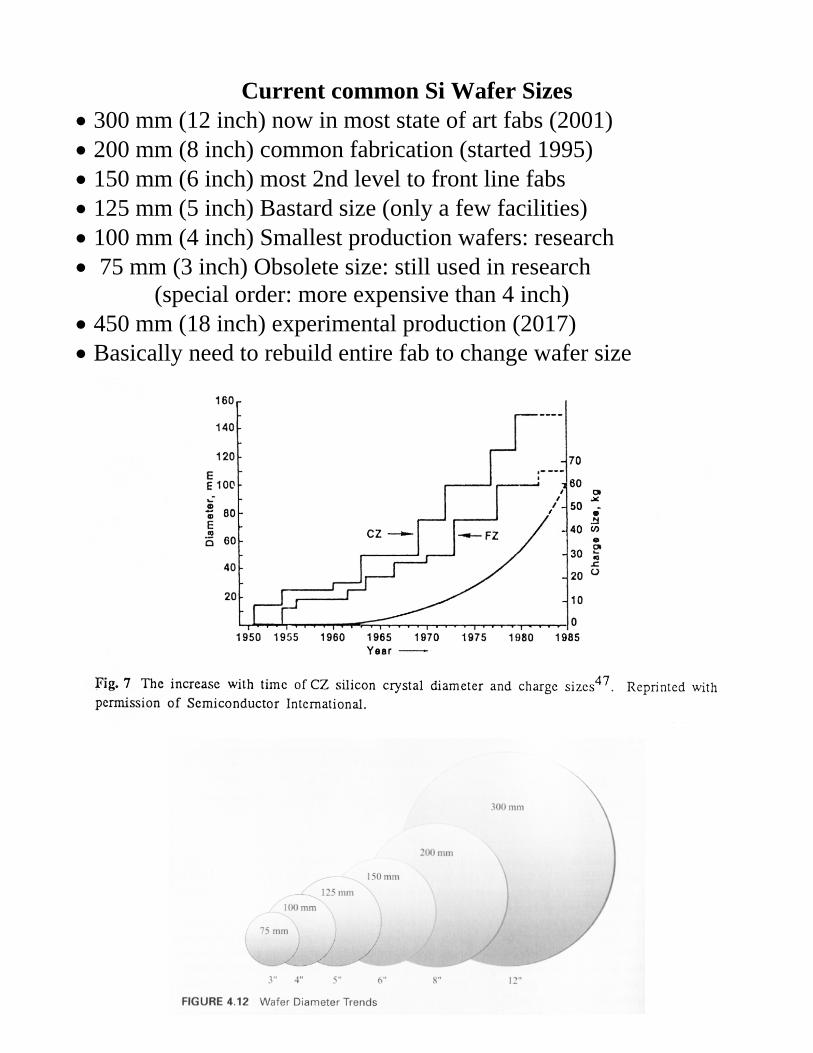
Current common Si Wafer Sizes 300 mm (12 inch) now in most state of art fabs (2001) 200 mm (8 inch) common fabrication (started 1995) 150 mm (6 inch) most 2nd level to front line fabs 125 mm (5 inch) Bastard size (only a few facilities) 100 mm (4 inch) Smallest production wafers: research 75 mm (3 inch) Obsolete size: still used in research (special order: more expensive than 4 inch) 450 mm (18 inch) experimental production (2017) Basically need to rebuild entire fab to change wafer size
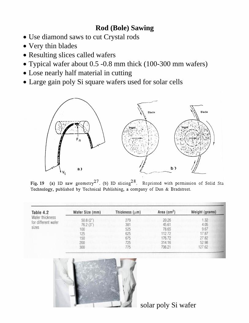
Rod (Bole) Sawing Use diamond saws to cut Crystal rods Very thin blades Resulting slices called wafers Typical wafer about 0.5 -0.8 mm thick (100-300 mm wafers) Lose nearly half material in cutting Large gain poly Si square wafers used for solar cells
solar poly Si wafer
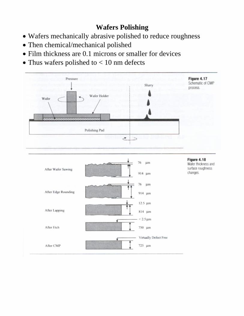
Wafers Polishing Wafers mechanically abrasive polished to reduce roughness Then chemical/mechanical polished Film thickness are 0.1 microns or smaller for devices Thus wafers polished to < 10 nm defects
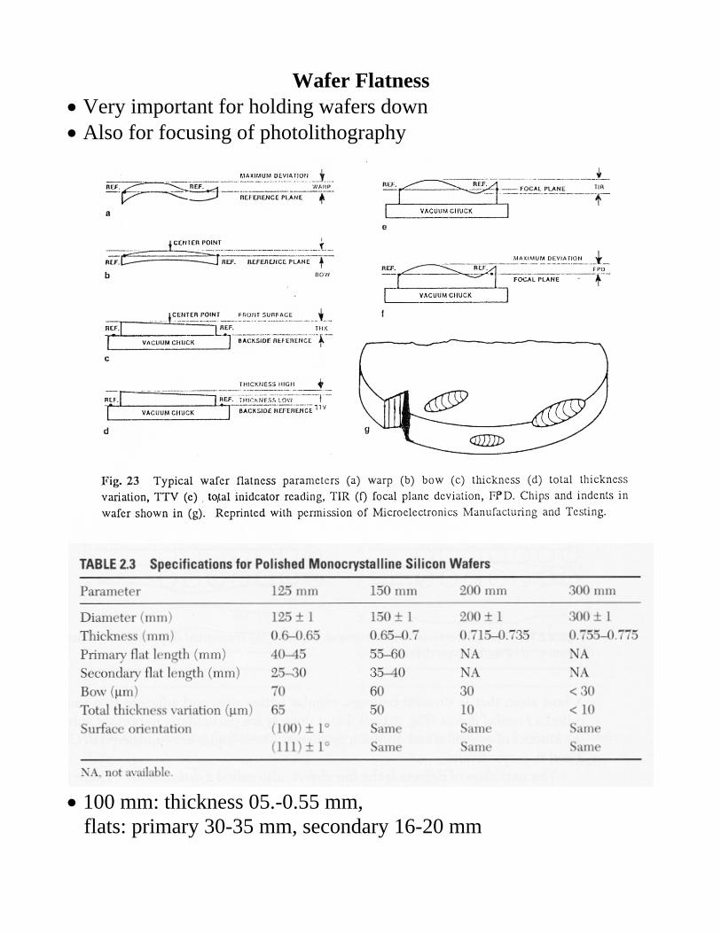
Wafer Flatness Very important for holding wafers down Also for focusing of photolithography
100 mm: thickness 05.-0.55 mm, flats: primary 30-35 mm, secondary 16-20 mm
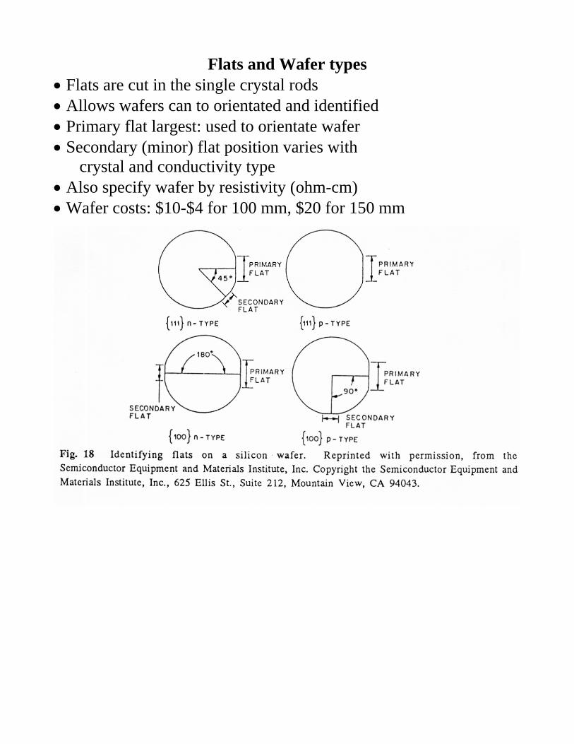
Flats and Wafer types Flats are cut in the single crystal rods Allows wafers can to orientated and identified Primary flat largest: used to orientate wafer Secondary (minor) flat position varies with crystal and conductivity type Also specify wafer by resistivity (ohm-cm) Wafer costs: $10-$4 for 100 mm, $20 for 150 mm
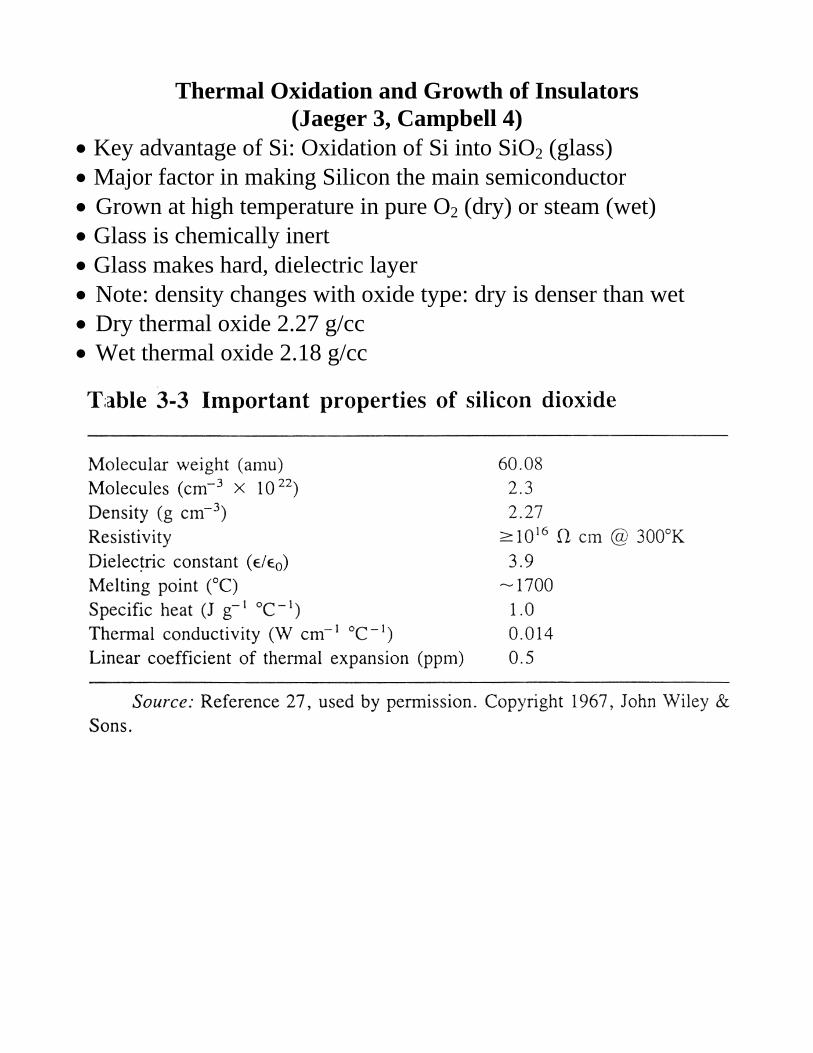
Thermal Oxidation and Growth of Insulators (Jaeger 3, Campbell 4)
Key advantage of Si: Oxidation of Si into SiO2 (glass) Major factor in making Silicon the main semiconductor Grown at high temperature in pure O2 (dry) or steam (wet) Glass is chemically inert Glass makes hard, dielectric layer Note: density changes with oxide type: dry is denser than wet Dry thermal oxide 2.27 g/cc Wet thermal oxide 2.18 g/cc
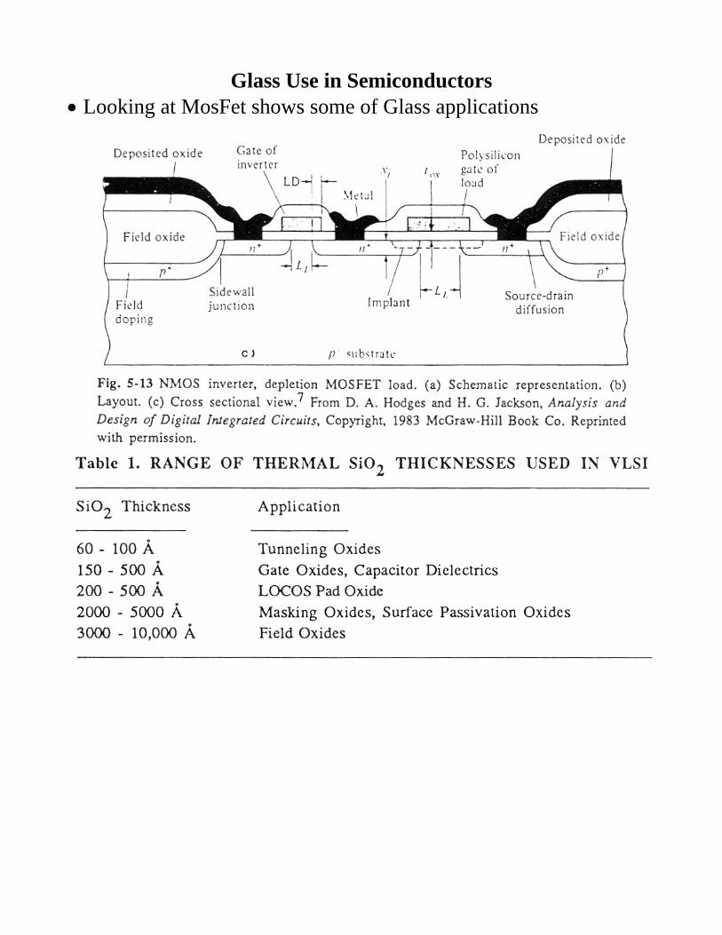
Glass Use in Semiconductors Looking at MosFet shows some of Glass applications
Uses of Oxide Films in IC’s Both grown oxides and Chemical Deposited (CVD) oxides
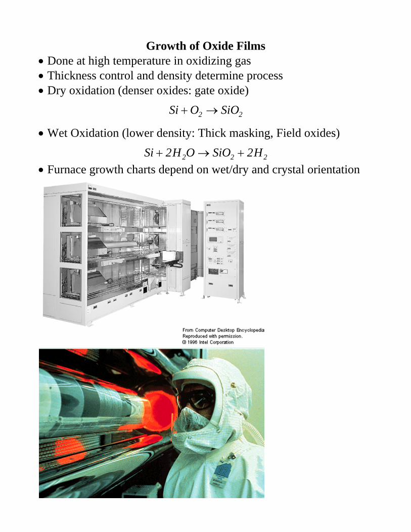
Growth of Oxide Films Done at high temperature in oxidizing gas Thickness control and density determine process Dry oxidation (denser oxides: gate oxide)
22 SiOOSi
Wet Oxidation (lower density: Thick masking, Field oxides)
222 H2SiOOH2Si
Furnace growth charts depend on wet/dry and crystal orientation
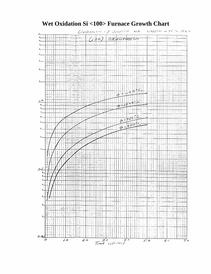
Wet Oxidation Si <100> Furnace Growth Chart
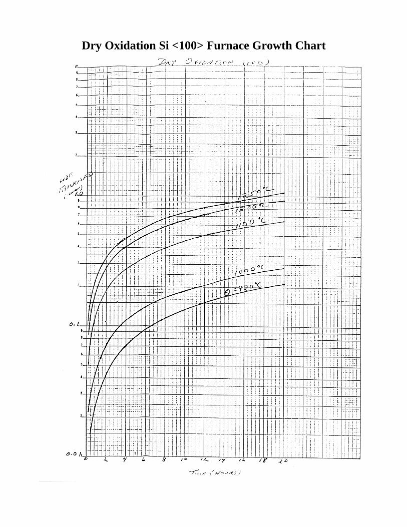
Dry Oxidation Si <100> Furnace Growth Chart
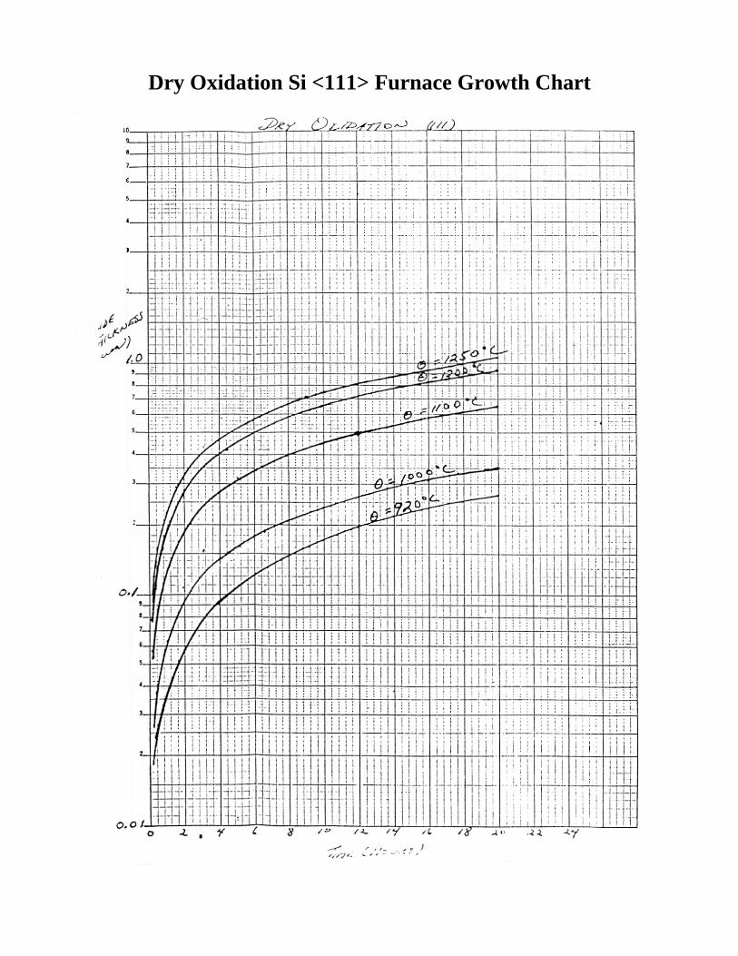
Dry Oxidation Si <111> Furnace Growth Chart
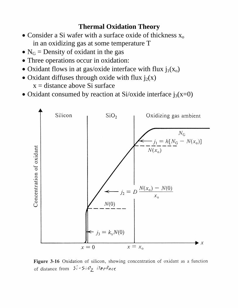
Thermal Oxidation Theory Consider a Si wafer with a surface oxide of thickness xo in an oxidizing gas at some temperature T NG = Density of oxidant in the gas Three operations occur in oxidation: Oxidant flows in at gas/oxide interface with flux j1(xo) Oxidant diffuses through oxide with flux j2(x) x = distance above Si surface Oxidant consumed by reaction at Si/oxide interface j3(x=0)
Thermal Oxidation Theory Flow at gas/SiO2 Surface: j1 Flux is atoms/molecules passing given surface per unite time (unites atoms/cm2sec) Oxidant declines from gas level NG to SiO2 surface due to flux into oxide Flux flow a mass transport process At oxide surface (x = x o) the flux into the oxide is
0G1 xNNhj
where h = mass transfer coefficient or proportionality constant N(xo) = oxidant concentration at SiO2 surface h is related to diffusion of oxidant from gas to oxide and thickness of slow moving gas layer at surface Within oxide (0 << x << xo): j2 Oxidant flow decreases linearly from the surface level
0
02 x
0NxNDxj
where D = Diffusion coefficient of oxidant in SiO2 N(0) = oxidant concentration at Si surface Related to Fick's diffusion law
Reaction of Oxide at Si Surface: j3 Reaction Rate of oxide in Si surface
0Nkxj s03
where ks = reaction rate constant Relating Flux at Interfaces Oxidant is consumed only at Si: Thus under steady state
321 jjj
Thus solving for the oxidant concentration at 0 and xo
D
xk
h
k1
N0N
0ss
G
D
xk
h
k1
D
xk1N
xN0ss
0sG
0
Growth of oxide thickness is related to reaction rate by
0Nk
dt
dx s0
where = no. of oxidant molecules used per unit oxide volume = 2.2x1022 cm-2 for O2 (Dry oxidation) = 4.4x1022 cm-2 for H2O (Wet oxidation)
Thermal Oxidation Solutions: Grove's Law Combining this with N(0) formula
D
xk
h
k1
Nk
dt
dx
0ss
Gs0
Deal and Grove (1965) solved this assuming xo(t=0) = xi
tBAxx 020
with
h
1
k
1D2A
s
GDN2
B
B
Axx i2i
Thus start with film xi which is defined to have taken time and grow for additional time t2 then get film
20 tx0x
ie: Result same as growing the film continuously for time t = t2 +
Does not matter which oxidation process used for xi time used is calculated for the process of the new growth not for process used to actually grow oxide Then solve the quadratic equation for x0, using A, B &
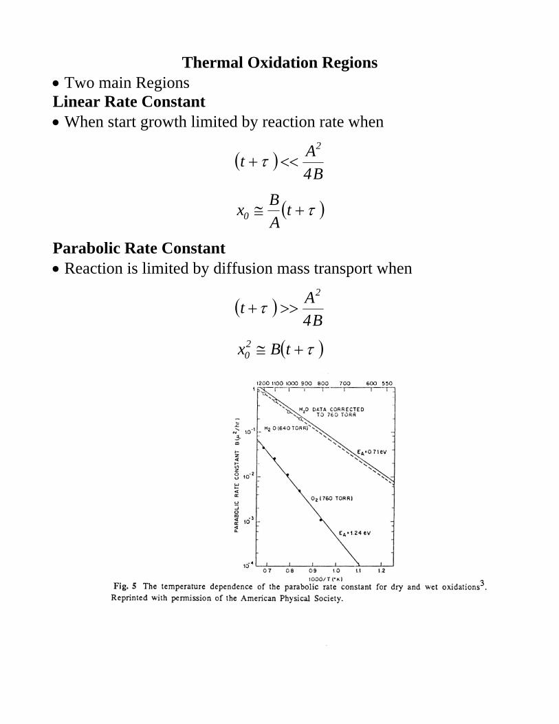
Thermal Oxidation Regions Two main Regions Linear Rate Constant When start growth limited by reaction rate when
B4
At
2
tA
Bx0
Parabolic Rate Constant Reaction is limited by diffusion mass transport when
B4
At
2
tBx20
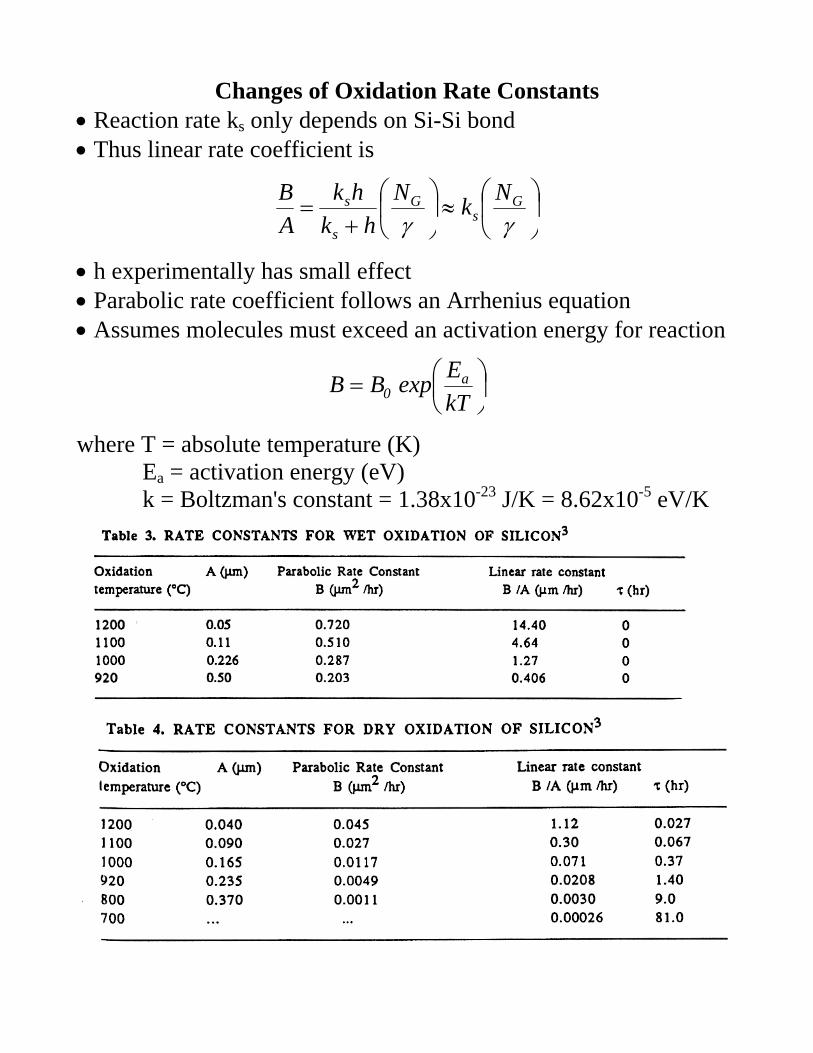
Changes of Oxidation Rate Constants Reaction rate ks only depends on Si-Si bond Thus linear rate coefficient is
Gs
G
s
s Nk
N
hk
hk
A
B
h experimentally has small effect Parabolic rate coefficient follows an Arrhenius equation Assumes molecules must exceed an activation energy for reaction
kT
EexpBB a
0
where T = absolute temperature (K) Ea = activation energy (eV) k = Boltzman's constant = 1.38x10⁻²³ J/K = 8.62x10⁻⁵ eV/K
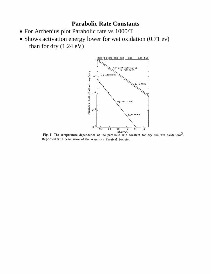
Parabolic Rate Constants For Arrhenius plot Parabolic rate vs 1000/T Shows activation energy lower for wet oxidation (0.71 ev) than for dry (1.24 eV)
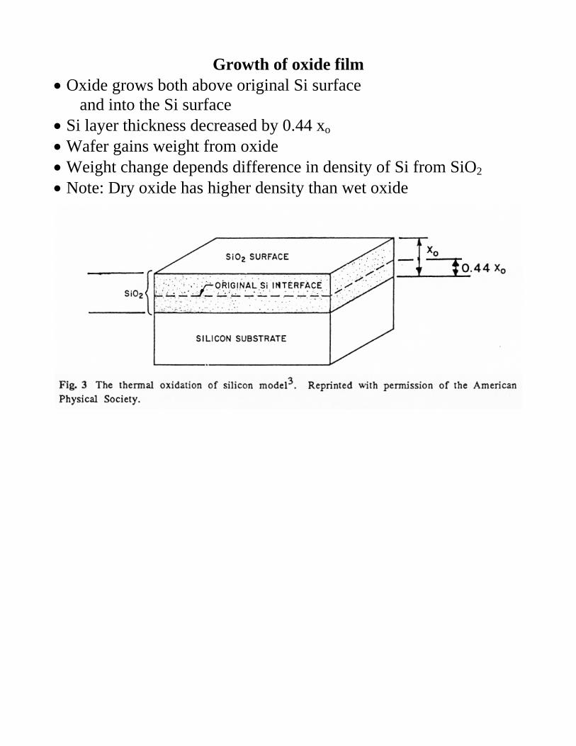
Growth of oxide film Oxide grows both above original Si surface and into the Si surface Si layer thickness decreased by 0.44 xo Wafer gains weight from oxide Weight change depends difference in density of Si from SiO2 Note: Dry oxide has higher density than wet oxide
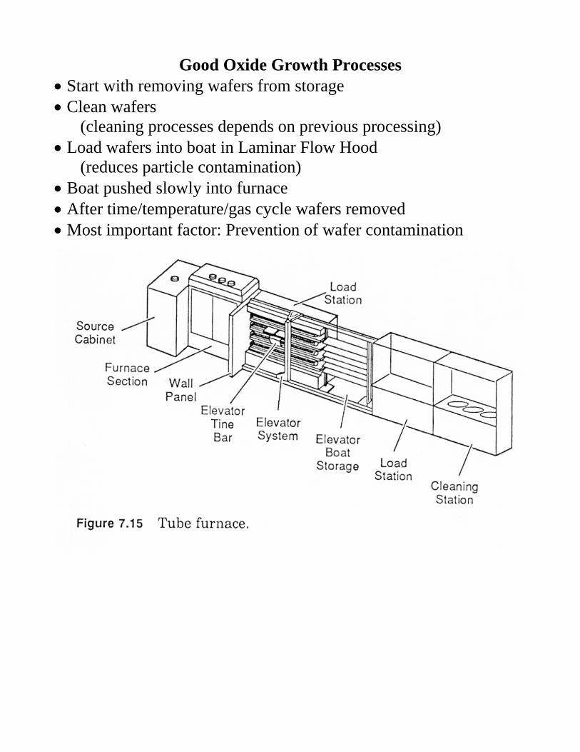
Good Oxide Growth Processes Start with removing wafers from storage Clean wafers (cleaning processes depends on previous processing) Load wafers into boat in Laminar Flow Hood (reduces particle contamination) Boat pushed slowly into furnace After time/temperature/gas cycle wafers removed Most important factor: Prevention of wafer contamination
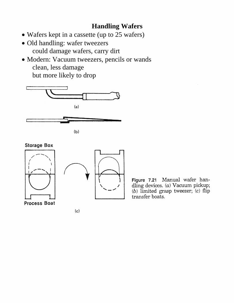
Handling Wafers Wafers kept in a cassette (up to 25 wafers) Old handling: wafer tweezers could damage wafers, carry dirt Modern: Vacuum tweezers, pencils or wands clean, less damage but more likely to drop
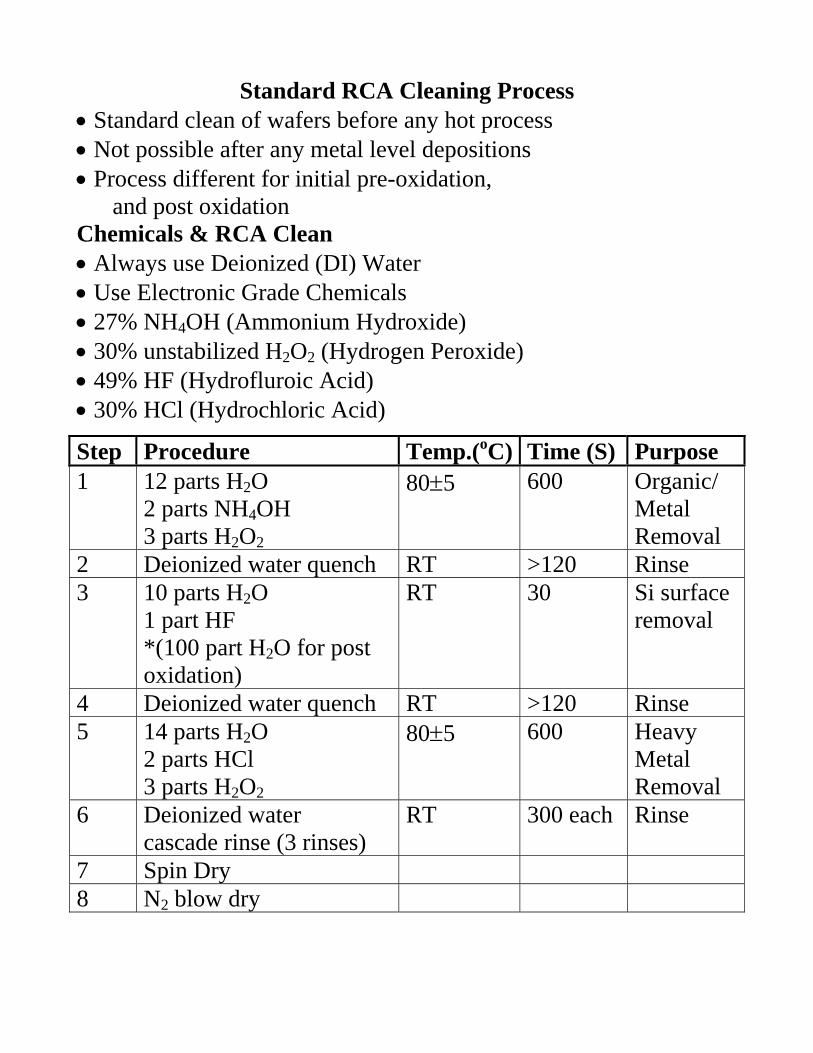
Standard RCA Cleaning Process Standard clean of wafers before any hot process Not possible after any metal level depositions Process different for initial pre-oxidation, and post oxidation Chemicals & RCA Clean Always use Deionized (DI) Water Use Electronic Grade Chemicals 27% NH4OH (Ammonium Hydroxide) 30% unstabilized H2O2 (Hydrogen Peroxide) 49% HF (Hydrofluroic Acid) 30% HCl (Hydrochloric Acid)
Step Procedure Temp.(oC) Time (S) Purpose 1 12 parts H2O
2 parts NH4OH 3 parts H2O2
805 600 Organic/ Metal Removal
2 Deionized water quench RT >120 Rinse 3 10 parts H2O
1 part HF *(100 part H2O for post oxidation)
RT 30 Si surface removal
4 Deionized water quench RT >120 Rinse 5 14 parts H2O
2 parts HCl 3 parts H2O2
805 600 Heavy Metal Removal
6 Deionized water cascade rinse (3 rinses)
RT 300 each Rinse
7 Spin Dry 8 N2 blow dry
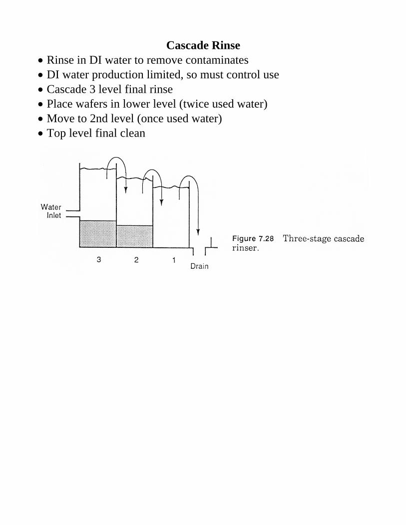
Cascade Rinse Rinse in DI water to remove contaminates DI water production limited, so must control use Cascade 3 level final rinse Place wafers in lower level (twice used water) Move to 2nd level (once used water) Top level final clean
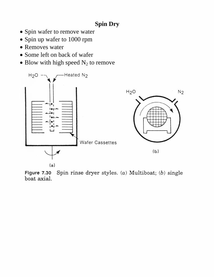
Spin Dry Spin wafer to remove water Spin up wafer to 1000 rpm Removes water Some left on back of wafer Blow with high speed N2 to remove
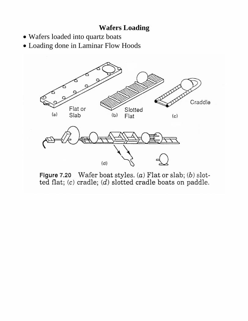
Wafers Loading Wafers loaded into quartz boats Loading done in Laminar Flow Hoods
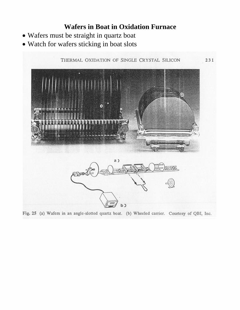
Wafers in Boat in Oxidation Furnace Wafers must be straight in quartz boat Watch for wafers sticking in boat slots
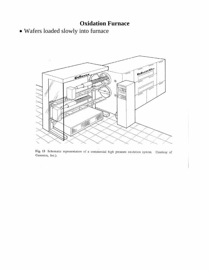
Oxidation Furnace Wafers loaded slowly into furnace
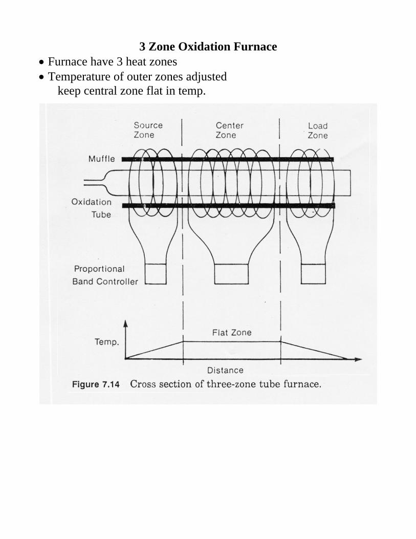
3 Zone Oxidation Furnace Furnace have 3 heat zones Temperature of outer zones adjusted keep central zone flat in temp.
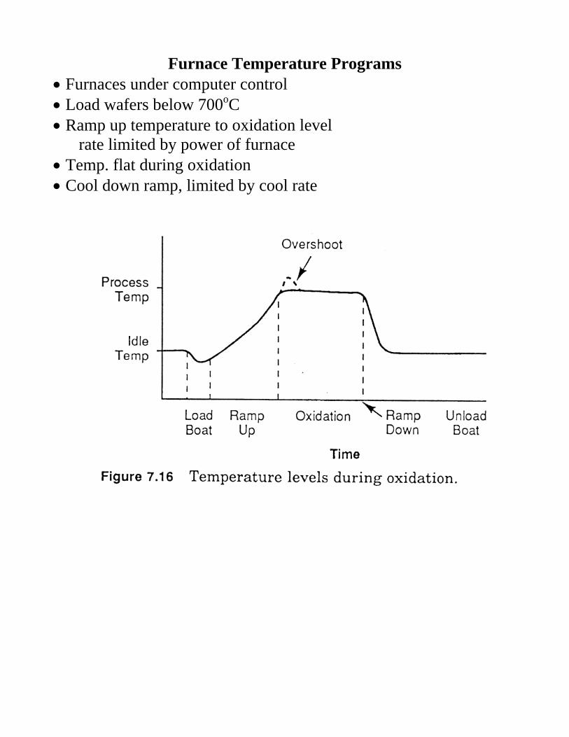
Furnace Temperature Programs Furnaces under computer control Load wafers below 700oC Ramp up temperature to oxidation level rate limited by power of furnace Temp. flat during oxidation Cool down ramp, limited by cool rate
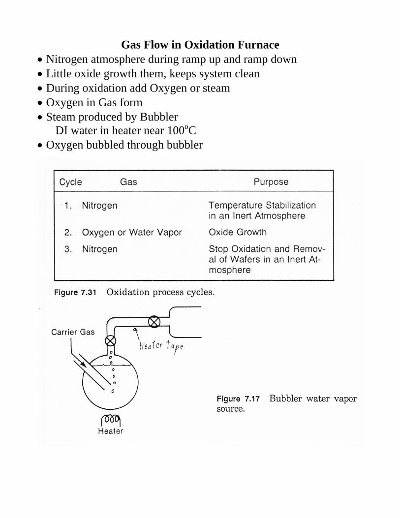
Gas Flow in Oxidation Furnace Nitrogen atmosphere during ramp up and ramp down Little oxide growth them, keeps system clean During oxidation add Oxygen or steam Oxygen in Gas form Steam produced by Bubbler DI water in heater near 100oC Oxygen bubbled through bubbler
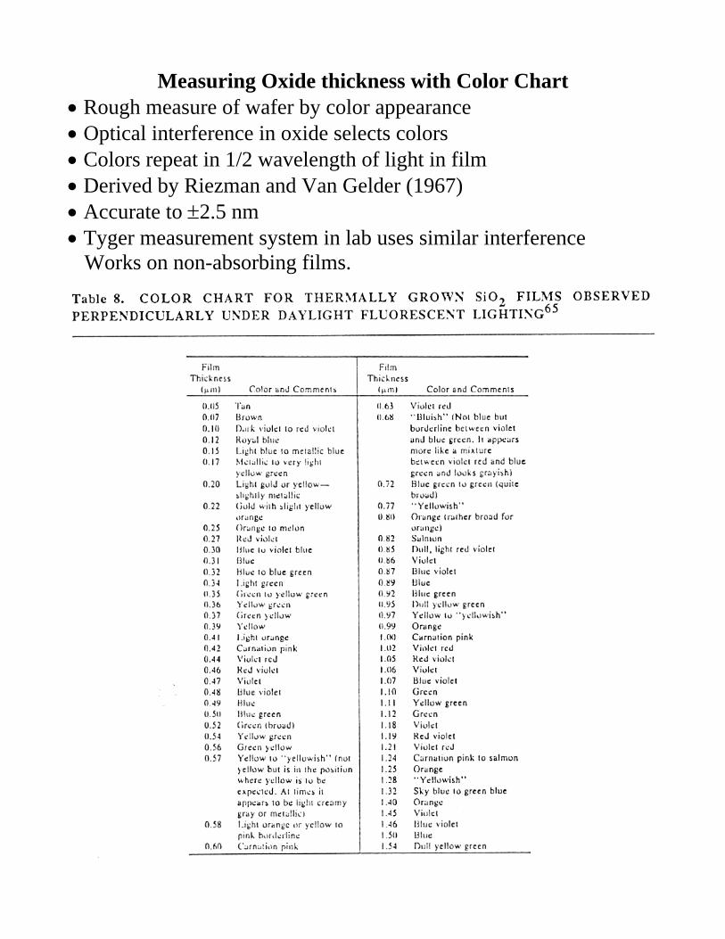
Measuring Oxide thickness with Color Chart Rough measure of wafer by color appearance Optical interference in oxide selects colors Colors repeat in 1/2 wavelength of light in film Derived by Riezman and Van Gelder (1967) Accurate to 2.5 nm Tyger measurement system in lab uses similar interference Works on non-absorbing films.
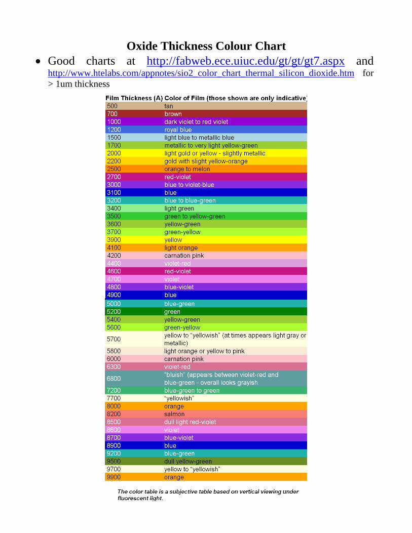
Oxide Thickness Colour Chart Good charts at http://fabweb.ece.uiuc.edu/gt/gt/gt7.aspx and
http://www.htelabs.com/appnotes/sio2_color_chart_thermal_silicon_dioxide.htm for > 1um thickness
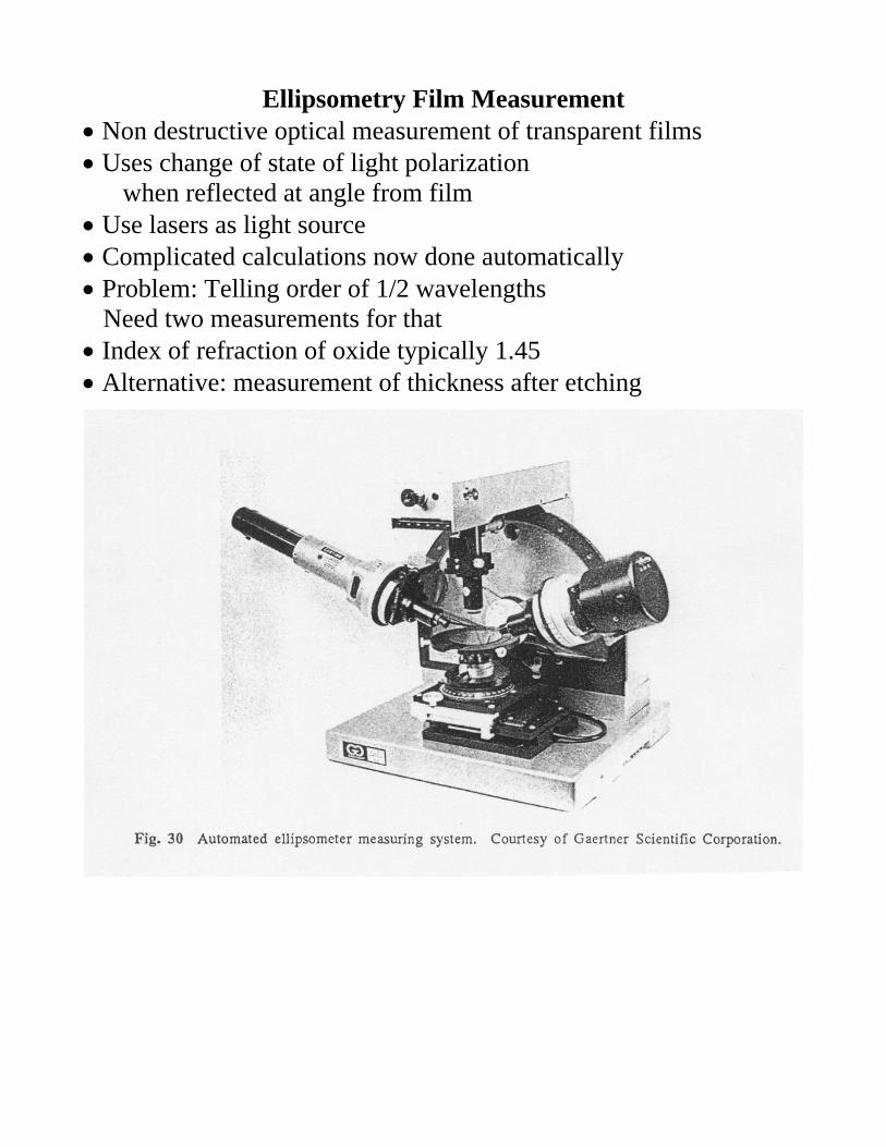
Ellipsometry Film Measurement Non destructive optical measurement of transparent films Uses change of state of light polarization when reflected at angle from film Use lasers as light source Complicated calculations now done automatically Problem: Telling order of 1/2 wavelengths Need two measurements for that Index of refraction of oxide typically 1.45 Alternative: measurement of thickness after etching
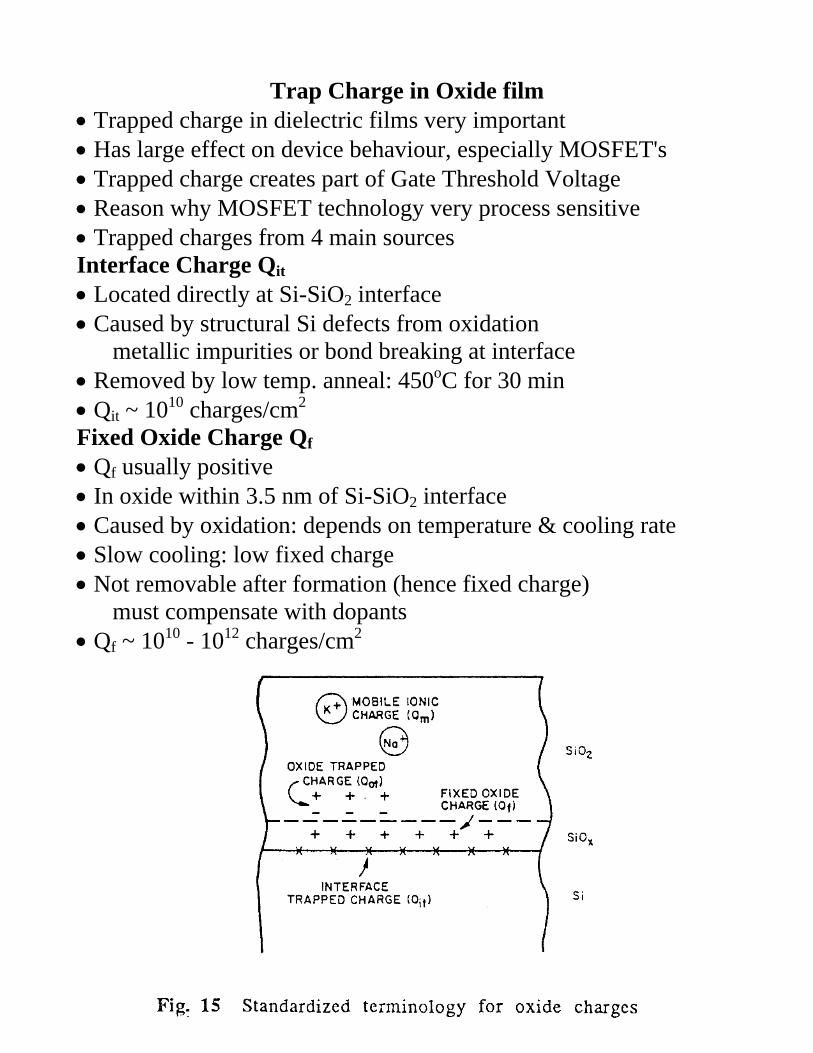
Trap Charge in Oxide film Trapped charge in dielectric films very important Has large effect on device behaviour, especially MOSFET's Trapped charge creates part of Gate Threshold Voltage Reason why MOSFET technology very process sensitive Trapped charges from 4 main sources Interface Charge Qit Located directly at Si-SiO2 interface Caused by structural Si defects from oxidation metallic impurities or bond breaking at interface Removed by low temp. anneal: 450oC for 30 min Qit ~ 1010 charges/cm2 Fixed Oxide Charge Qf Qf usually positive In oxide within 3.5 nm of Si-SiO2 interface Caused by oxidation: depends on temperature & cooling rate Slow cooling: low fixed charge Not removable after formation (hence fixed charge) must compensate with dopants Qf ~ 1010 - 1012 charges/cm2
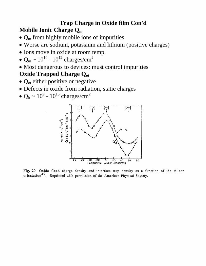
Trap Charge in Oxide film Con'd Mobile Ionic Charge Qm Qm from highly mobile ions of impurities Worse are sodium, potassium and lithium (positive charges) Ions move in oxide at room temp. Qm ~ 1010 - 1012 charges/cm2 Most dangerous to devices: must control impurities Oxide Trapped Charge Qot Qot either positive or negative Defects in oxide from radiation, static charges Qit ~ 109 - 1013 charges/cm2
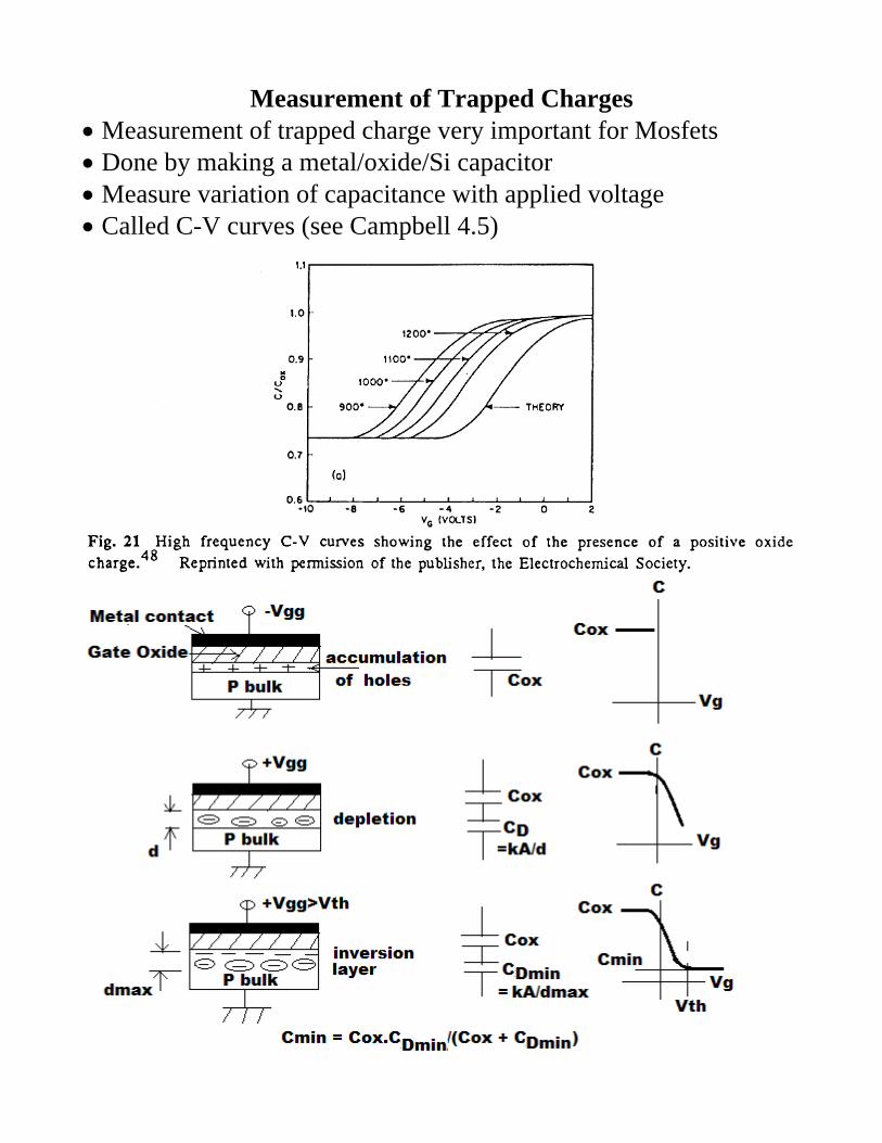
Measurement of Trapped Charges Measurement of trapped charge very important for Mosfets Done by making a metal/oxide/Si capacitor Measure variation of capacitance with applied voltage Called C-V curves (see Campbell 4.5)


![th LHCC Meeting RD50 Status Report · •Nitrogen-enriched FZ silicon wafers (NitroSil project) • N-enriched wafers [Topsil] showed after irradiation a lower trap density • Defect](https://img.pdfslide.us/doc/110x75/5e5576e05481c15ed129581c/th-lhcc-meeting-rd50-status-report-anitrogen-enriched-fz-silicon-wafers-nitrosil.jpg)