Chapter 3
Pulsed laser deposition of
PZT and PLZT
A lower growth temperature of PZT films is favored for integration of these
films for MEMS application. This chapter gives a detailed account of the
work carried for the growth of PZT films at relatively lower substrate tem-
perature. The deposition of PZT on PtSi substrates itself is a challenging
task since Pb is highly volatile. The targets used were 2% and 10% excess
Pb added to the PZT for maintaining the stoichiometry of the films.La is
substituted as donar dopant in PZT to form PLZT. Effect of buffer layer
on the structural and electrical properties is also investigated.The use of
ZnO buffer layers has reduced the temperature of crystallisation of PZT to
3000C. The electrical characterizations of the devices is discussed in detail.
87
88 Pulsed laser deposition of PZT and PLZT
3.1 Introduction
Pb-based ferroelectric thin film such as Pb(Zr,Ti)O3 (PZT)and (Pb,La)
(Zr,Ti) O3 (PLZT) are widely attracted because of their excellent ferro-
electric , dielectric, pyroelectric and piezoelectric properties. Piezoelectric
lead zirconate titanate (PZT) thin films have been employed extensively
in micro actuators for micro electro mechanical system (MEMS). Recently
PLZT has got attention because of its potential to integrate with the semi-
conductor devices. The synthesis of PZT ferroelectric film is difficult. Re-
cently the films of pure perovskite phase were successfully prepared with
electrical properties comparable to that of ceramic form but its dielectric
constant is inferior to bulk ceramic. The problem originate from the diffi-
culty in the control of composition which is due to the inherent Pb2+ ion
loss occurring during the thin film deposition. The techniques which have
been successful for deposition of PZT on single crystal cannot be applied
directly to grow PZT films on silicon or Pt coated substrate. A large por-
tion of pyrochlore phase is always present in thin films grown by sol gel,
chemical solution method, laser ablation and sputtering[86–88].
The popular thin film deposition techniques for PZT/PLZT are sol-gel,
sputtering, metal-organic chemical vapor deposition (MOCVD) and pulsed
laser deposition. For preparing ferroelectric PZT films, magnetron sput-
tering has conventionally been used. This method has some disadvantages
such as low deposition rate and large variation in composition. These dis-
advantages are overcome in other methods like sol-gel technique, MOCVD
and laser ablation. Sol-gel has the advantages of high purity, uniform film
thickness and easy control of composition and crystallinity. But a sol-gel
derived PZT thin film has problems such as low deposition rate and rela-
Experimental Details 89
tively high crystallization temperature. The PLD technique possesses over-
whelming advantage of easiness in control of stoichiometric composition in
thin film deposition. It is suitable for growing multicomponent oxide thin
films. Further in contrast with sol-gel and MOCVD which require special
source materials , the laser ablation can use the ceramic target as a source
material[87].
The PZT films of good electrical characteristics can be obtained on Si
substrates using PLD technique such as sequential deposition of ZrO2, TiO2
and PbO layers [89], direct ablation of PZT target with excess PbO [86],
depositing a perovskite buffer layers or post annealing of low temperature
deposited films [87].
Most defects in PZT films are due to vacancies of lead and oxygen. PbO
is volatile and PZT can accommodate large amounts of lead and oxygen
vacancies which can interact with one another. Lead loss is avoided by
adding 2% and 10% excess lead to the ablation targets . Oxygen vacancy
formation is inhibited by including donor dopants in PZT [90, 91].
In this chapter pulsed laser deposition of PZT/PLZT thin films are
described. The chapter is divided into two parts. Section 3.3 focuses on
the pulsed laser deposition of PZT/PLZT for obtaining pure perovskite
phase. The effect of buffer layer on the microstructure of PZT/PLZT is
discussed. Section 3.4 details the electrical characterization of PZT/PLZT
ferroelectric devices.
3.2 Experimental Details
The PZT and PLZT targets for PLD is synthesised using solid state reac-
tion of PbO, TiO2 and ZrO2. La donar dopant is added to PZT during
90 Pulsed laser deposition of PZT and PLZT
material preparation. PZT thin films were ablated using fourth harmonics
of Nd:YAG laser (266nm). The repetition frequency was 10Hz with a pulse
width of 8-9ns. The laser fluence was kept at 2J/cm2.
The target was fixed at an angle 450 to the direction of laser beam
and it was rotated at a constant rpm during the laser deposition, so that
pitting of the target surface by the laser beam will be uniform.The focused
energy of the high-energy laser ionises the target material and the ’plume”
produced spreads out in the forward direction towards the substrates and
it is slightly divergent. The substrate is placed at a distance 4cm to the
target surface.The gas (oxygen) is bled into the vacuum chamber contin-
uously at a fixed flow rate, while the chamber is simultaneously pumped
to maintain a constant background pressure during deposition. The flow
of oxygen ambient gas is controlled by using a mass flow controller.The
substrate temperature (Ts) was varied from 3000C - 6000C. The oxygen
partial pressure in the chamber is 0.15mbar.
The crystallinity of thin films was determined by x ray diffraction
(XRD) using CuKα radiation(λ =1.5418A0). Thickness of the samples
were measured using Dektak 6M surface profiler. The electrical character-
ization of thin films were carried out using I-V and C-V measurements.
The ferroelectric behavior of the films were carried out using Sawyer Tower
circuit.
3.3 Pure perovskite phase formation of PZT/PLZT
thin films
Figure 3.1 shows the XRD pattern of PZT target used for ablation. The
XRD pattern clearly indicates a tetragonal perovskite phase. La substi-
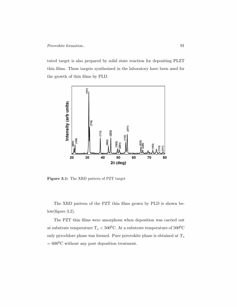
Perovskite formation.. 91
tuted target is also prepared by solid state reaction for depositing PLZT
thin films. These targets synthesized in the laboratory have been used for
the growth of thin films by PLD.
Figure 3.1: The XRD pattern of PZT target
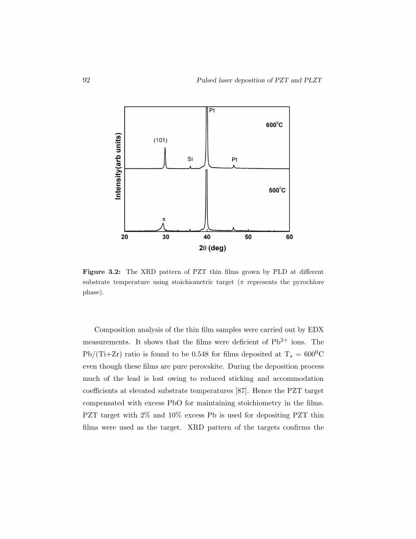
The XRD pattern of the PZT thin films grown by PLD is shown be-
low(figure 3.2).
The PZT thin films were amorphous when deposition was carried out
at substrate temperature Ts < 5000C. At a substrate temperature of 5000C
only pyrochlore phase was formed. Pure perovskite phase is obtained at Ts
= 6000C without any post deposition treatment.
92 Pulsed laser deposition of PZT and PLZT
Figure 3.2: The XRD pattern of PZT thin films grown by PLD at different
substrate temperature using stoichiometric target (π represents the pyrochlore
phase).
Composition analysis of the thin film samples were carried out by EDX
measurements. It shows that the films were deficient of Pb2+ ions. The
Pb/(Ti+Zr) ratio is found to be 0.548 for films deposited at Ts = 6000C
even though these films are pure perovskite. During the deposition process
much of the lead is lost owing to reduced sticking and accommodation
coefficients at elevated substrate temperatures [87]. Hence the PZT target
compensated with excess PbO for maintaining stoichiometry in the films.
PZT target with 2% and 10% excess Pb is used for depositing PZT thin
films were used as the target. XRD pattern of the targets confirms the
Perovskite formation.. 93
tetragonal perovskite phase in the starting material. Pb1.02Zr0.5Ti0.5O3
(P2ZT) and Pb1.1Zr0.5Ti0.5O3) (P10ZT) were used for the growth of thin
films by PLD.
XRD pattern of P2ZT and P10ZT on PtSi substrates at different sub-
strate temperature shows the same pattern as that of PZT. The films de-
posited at Ts = 6000C is crystalline perovskite wheras films deposited at
Ts = 5000C showed pyrochlore phase. All the films deposited below 5000C
were amorphous.
The composition analysis of these films shows that the films are stoi-
chiometric when the target is compensated with 2% excess Pb. The ratio
Pb/(Zr+Ti) is nearly 1 for films deposited at a substrate temperature of
6000C.
It is a common practise to include donor dopants in PZT to improve
electrical and optical properties. The most common A site dopants are
trivalent lanthanum (La). Lanthanum donor dopants in PZT compensate
the lead vacancy thereby inhibiting the formation of oxygen vacancies [92].
PLZT thin films are ablated using the fourth harmonics of Nd:YAG laser.
The conditions are same as that for the deposition of PZT thin films.
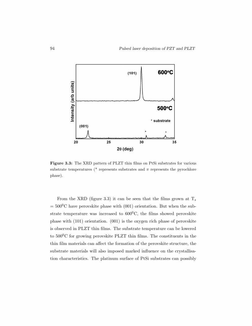
94 Pulsed laser deposition of PZT and PLZT
Figure 3.3: The XRD pattern of PLZT thin films on PtSi substrates for various
substrate temperatures (* represents substrates and π represents the pyrochlore
phase).
From the XRD (figure 3.3) it can be seen that the films grown at Ts
= 5000C have perovskite phase with (001) orientation. But when the sub-
strate temperature was increased to 6000C, the films showed perovskite
phase with (101) orientation. (001) is the oxygen rich phase of perovskite
is observed in PLZT thin films. The substrate temperature can be lowered
to 5000C for growing perovskite PLZT thin films. The constituents in the
thin film materials can affect the formation of the perovskite structure, the
substrate materials will also imposed marked influence on the crystallisa-
tion characteristics. The platinum surface of PtSi substrates can possibly
Perovskite formation.. 95
trigger the formation of the perovskite phase at lower temperature [87].
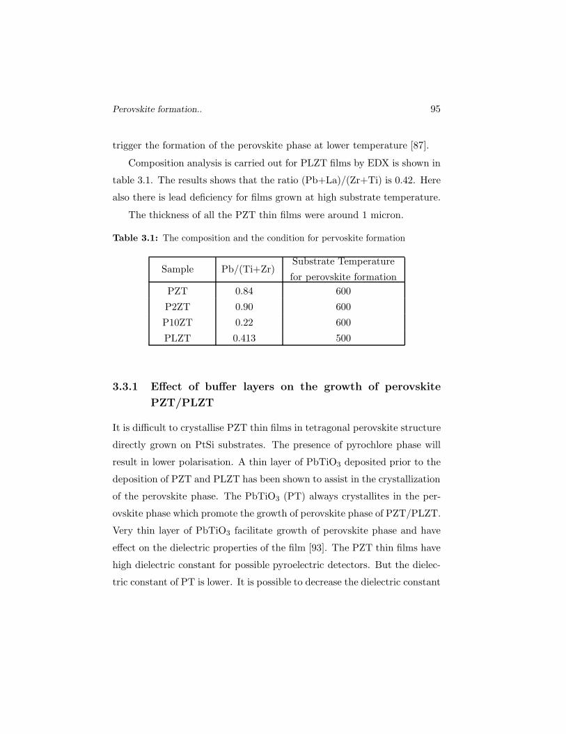
Composition analysis is carried out for PLZT films by EDX is shown in
table 3.1. The results shows that the ratio (Pb+La)/(Zr+Ti) is 0.42. Here
also there is lead deficiency for films grown at high substrate temperature.
The thickness of all the PZT thin films were around 1 micron.
Table 3.1: The composition and the condition for pervoskite formation
Sample Pb/(Ti+Zr)Substrate Temperature
for perovskite formation
PZT 0.84 600
P2ZT 0.90 600
P10ZT 0.22 600
PLZT 0.413 500
3.3.1 Effect of buffer layers on the growth of perovskite
PZT/PLZT
It is difficult to crystallise PZT thin films in tetragonal perovskite structure
directly grown on PtSi substrates. The presence of pyrochlore phase will
result in lower polarisation. A thin layer of PbTiO3 deposited prior to the
deposition of PZT and PLZT has been shown to assist in the crystallization
of the perovskite phase. The PbTiO3 (PT) always crystallites in the per-
ovskite phase which promote the growth of perovskite phase of PZT/PLZT.
Very thin layer of PbTiO3 facilitate growth of perovskite phase and have
effect on the dielectric properties of the film [93]. The PZT thin films have
high dielectric constant for possible pyroelectric detectors. But the dielec-
tric constant of PT is lower. It is possible to decrease the dielectric constant
96 Pulsed laser deposition of PZT and PLZT
of PZT by using a thin layer of PT as buffer. The PT buffer layer can assist
in perovskite formation; at the same time decreases the dielectric constant
which is suitable for pyroelectric application. The formation of perovskite
phase of PZT at lower substrate temperature with PbTiO3 thin layer as
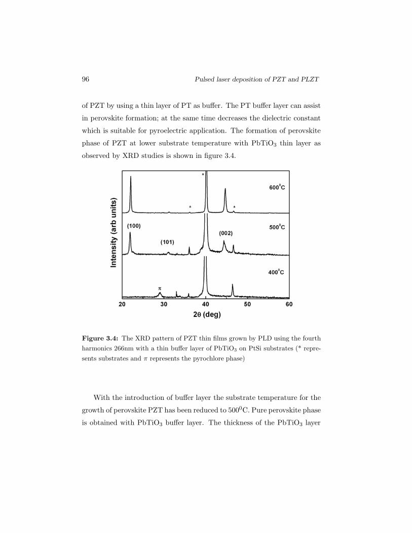
observed by XRD studies is shown in figure 3.4.
Figure 3.4: The XRD pattern of PZT thin films grown by PLD using the fourth
harmonics 266nm with a thin buffer layer of PbTiO3 on PtSi substrates (* repre-
sents substrates and π represents the pyrochlore phase)
With the introduction of buffer layer the substrate temperature for the
growth of perovskite PZT has been reduced to 5000C. Pure perovskite phase
is obtained with PbTiO3 buffer layer. The thickness of the PbTiO3 layer
Perovskite formation.. 97
is 80nm.
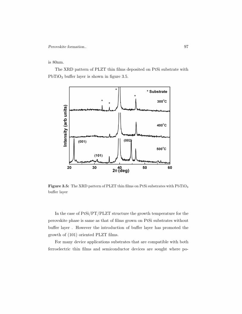
The XRD pattern of PLZT thin films deposited on PtSi substrate with
PbTiO3 buffer layer is shown in figure 3.5.
Figure 3.5: The XRD pattern of PLZT thin films on PtSi substrates with PbTiO3
buffer layer
In the case of PtSi/PT/PLZT structure the growth temperature for the
perovskite phase is same as that of films grown on PtSi substrates without
buffer layer . However the introduction of buffer layer has promoted the
growth of (101) oriented PLZT films.
For many device applications substrates that are compatible with both
ferroelectric thin films and semiconductor devices are sought where po-
98 Pulsed laser deposition of PZT and PLZT
tential direct integration of ferroelectric with semiconductor is envisioned.
ZnO is emerging as an important wide bandgap semiconductor material for
devices operating in the ultraviolet. ZnO has intrinsic compatibility with
ferroelectric oxides as a semiconducting oxide. ZnO has also been used as
a buffer layer for PZT ferroelectric capacitors in PtSi and as the channel
layer for ferroelectric gate thin film transistors [89].
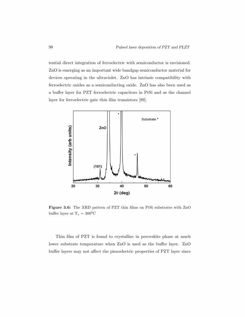
Figure 3.6: The XRD pattern of PZT thin films on PtSi substrates with ZnO
buffer layer at Ts = 3000C
Thin film of PZT is found to crystallize in perovskite phase at much
lower substrate temperature when ZnO is used as the buffer layer. ZnO
buffer layers may not affect the piezoelectric properties of PZT layer since
Perovskite formation.. 99
ZnO itself is a piezoelectric material. ZnO buffer layer has reduced the
substrate temperature for the growth of perovskite PZT films from 6000C
to 3000C. The XRD pattern of ZnO/PZT is shown in figure 3.6. ZnO buffer
layer promotes the growth of (101) oriented perovskite phase of PZT thin
films.
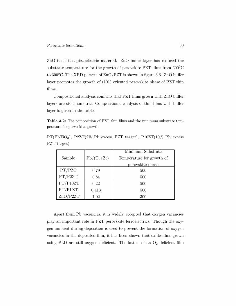
Compositional analysis confirms that PZT films grown with ZnO buffer
layers are stoichiometric. Compositional analysis of thin films with buffer
layer is given in the table.
Table 3.2: The composition of PZT thin films and the minimum substrate tem-
perature for pervoskite growth
PT(PbTiO3), P2ZT(2% Pb excess PZT target), P10ZT(10% Pb excess
PZT target)
Sample Pb/(Ti+Zr)
Minimum Substrate
Temperature for growth of
perovskite phase
PT/PZT 0.79 500
PT/P2ZT 0.84 500
PT/P10ZT 0.22 500
PT/PLZT 0.413 500
ZnO/P2ZT 1.02 300
Apart from Pb vacancies, it is widely accepted that oxygen vacancies
play an important role in PZT perovskite ferroelectrics. Though the oxy-
gen ambient during deposition is used to prevent the formation of oxygen
vacancies in the deposited film, it has been shown that oxide films grown
using PLD are still oxygen deficient. The lattice of an O2 deficient film
100 Pulsed laser deposition of PZT and PLZT
expands beyond the size reported for corresponding bulk ceramics. The in-
terfacial defect layers may originate from accumulation of oxygen vacancies.
Under the electric field oxygen vacancies migrate towards the electrode and
aggregate near the electrode interface. The perovskite structured titanate
could not afford a large population of point defects [92, 94].
In the case of conducting oxide electrodes or aqueous solution electrodes,
oxygen vacancies in the perovskite film in the region near the film electrode
interface can be compensated by the electrodes. Thus the use of this kind
of electrodes inhibits the accumulation of oxygen vacancies at the interface.
As a result no interfacial defect layer forms at ferroelectric oxide interfaces.
Oxide thin films have a wide range of properties covering insulators to
high temperature superconductors and from ferroelectric to ferromagnetic
materials. The growth of oxide thin films is an active field of research
[95, 96]. Perovskite conducting oxide La0.5Sr0.5CoO3(LSCO) is obtained
from ABO3 perovskite LaCoO3 by partial substitution of La3+ by Sr2+
[97, 98]. The similar crystal structure of LSCO with that of the perovskite
ferroelectrics makes it a potential candidate as electrode for ferroelectric
memory devices. The LSCO which is a conductive oxide electrode act as
oxygen vacancy sink of the PZT capacitors thereby reducing the fatigue
problem usually encountered while using conventional Pt electrode [99–
102]. The similar crystal structure of LSCO and perovskite ferroelectrics fa-
cilitates the easy growth of ferroelectrics over textured or epitaxially grown
LSCO layer [103, 104]. La0.5Sr0.5Co1−xNixO3 (LSCNO)is also widely used
as electrode for ferroelectric memory devices [105]. The partial substitution
of Co by Ni in La0.5Sr0.5CoO3 has been reported to increases the electrical
conductivity of LSCO thin films [106].
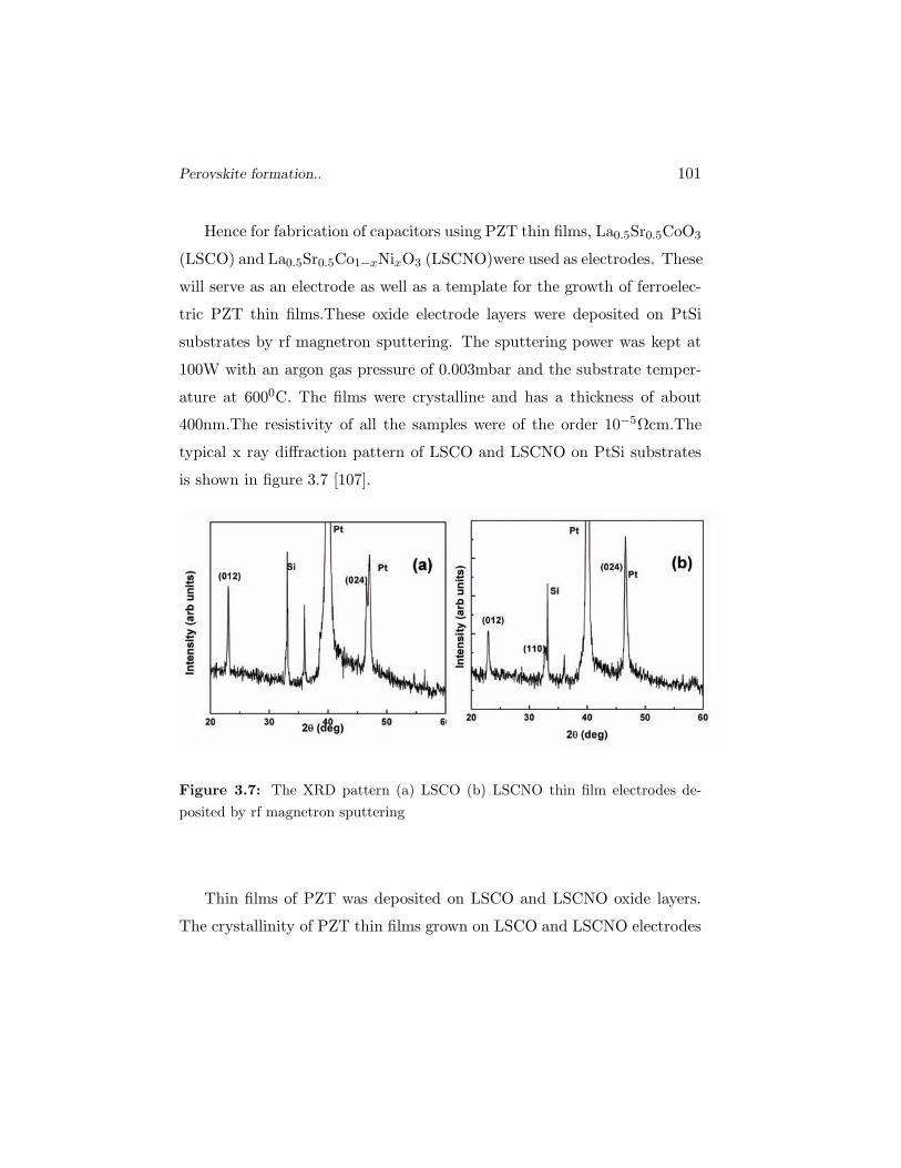
Perovskite formation.. 101
Hence for fabrication of capacitors using PZT thin films, La0.5Sr0.5CoO3
(LSCO) and La0.5Sr0.5Co1−xNixO3 (LSCNO)were used as electrodes. These
will serve as an electrode as well as a template for the growth of ferroelec-
tric PZT thin films.These oxide electrode layers were deposited on PtSi
substrates by rf magnetron sputtering. The sputtering power was kept at
100W with an argon gas pressure of 0.003mbar and the substrate temper-
ature at 6000C. The films were crystalline and has a thickness of about
400nm.The resistivity of all the samples were of the order 10−5Ωcm.The
typical x ray diffraction pattern of LSCO and LSCNO on PtSi substrates
is shown in figure 3.7 [107].
Figure 3.7: The XRD pattern (a) LSCO (b) LSCNO thin film electrodes de-
posited by rf magnetron sputtering
Thin films of PZT was deposited on LSCO and LSCNO oxide layers.
The crystallinity of PZT thin films grown on LSCO and LSCNO electrodes
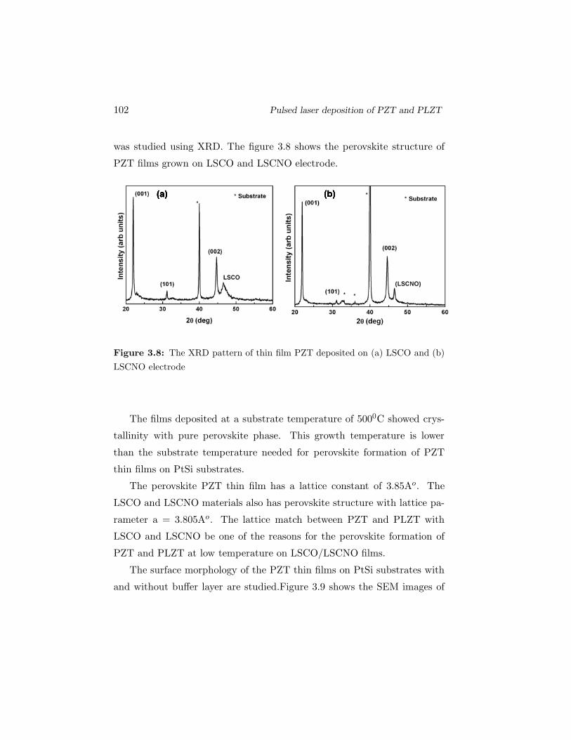
102 Pulsed laser deposition of PZT and PLZT
was studied using XRD. The figure 3.8 shows the perovskite structure of
PZT films grown on LSCO and LSCNO electrode.
Figure 3.8: The XRD pattern of thin film PZT deposited on (a) LSCO and (b)
LSCNO electrode
The films deposited at a substrate temperature of 5000C showed crys-
tallinity with pure perovskite phase. This growth temperature is lower
than the substrate temperature needed for perovskite formation of PZT
thin films on PtSi substrates.
The perovskite PZT thin film has a lattice constant of 3.85Ao. The
LSCO and LSCNO materials also has perovskite structure with lattice pa-
rameter a = 3.805Ao. The lattice match between PZT and PLZT with
LSCO and LSCNO be one of the reasons for the perovskite formation of
PZT and PLZT at low temperature on LSCO/LSCNO films.
The surface morphology of the PZT thin films on PtSi substrates with
and without buffer layer are studied.Figure 3.9 shows the SEM images of
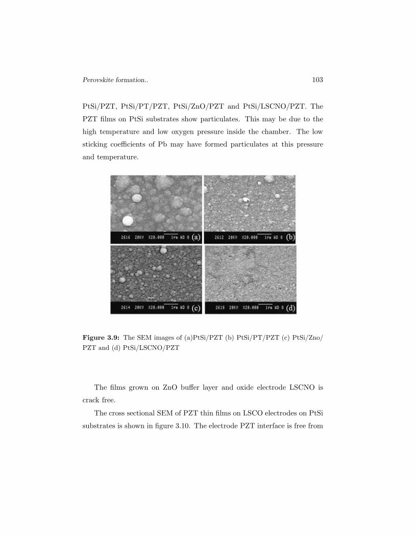
Perovskite formation.. 103
PtSi/PZT, PtSi/PT/PZT, PtSi/ZnO/PZT and PtSi/LSCNO/PZT. The
PZT films on PtSi substrates show particulates. This may be due to the
high temperature and low oxygen pressure inside the chamber. The low
sticking coefficients of Pb may have formed particulates at this pressure
and temperature.
Figure 3.9: The SEM images of (a)PtSi/PZT (b) PtSi/PT/PZT (c) PtSi/Zno/
PZT and (d) PtSi/LSCNO/PZT
The films grown on ZnO buffer layer and oxide electrode LSCNO is
crack free.
The cross sectional SEM of PZT thin films on LSCO electrodes on PtSi
substrates is shown in figure 3.10. The electrode PZT interface is free from
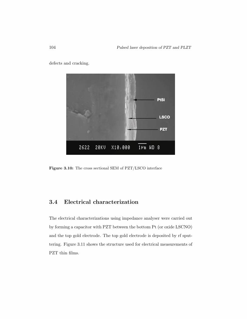
104 Pulsed laser deposition of PZT and PLZT
defects and cracking.
Figure 3.10: The cross sectional SEM of PZT/LSCO interface
3.4 Electrical characterization
The electrical characterizations using impedance analyser were carried out
by forming a capacitor with PZT between the bottom Pt (or oxide LSCNO)
and the top gold electrode. The top gold electrode is deposited by rf sput-
tering. Figure 3.11 shows the structure used for electrical measurements of
PZT thin films.
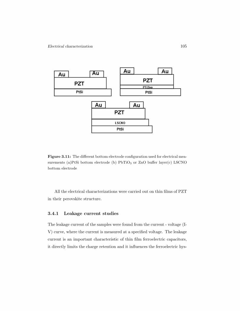
Electrical characterization 105
Figure 3.11: The different bottom electrode configuration used for electrical mea-
surements (a)PtSi bottom electrode (b) PbTiO3 or ZnO buffer layer(c) LSCNO
bottom electrode
All the electrical characterizations were carried out on thin films of PZT
in their perovskite structure.
3.4.1 Leakage current studies
The leakage current of the samples were found from the current - voltage (I-
V) curve, where the current is measured at a specified voltage. The leakage
current is an important characteristic of thin film ferroelectric capacitors,
it directly limits the charge retention and it influences the ferroelectric hys-
106 Pulsed laser deposition of PZT and PLZT
teresis loop. The leakage current is also a sensitive electrical probe to the
material quality of heterostructure as it is strongly dependent on mate-
rial aspects of the ferroelectric film and of electrode-ferroelectric interfaces
[107]. Capacitor with low leakage current is ideal for microelectronic device
application.
PtSi/PZT/Au and PtSi/PT/PZT/Au
The leakage current of all the samples were measured using constant current
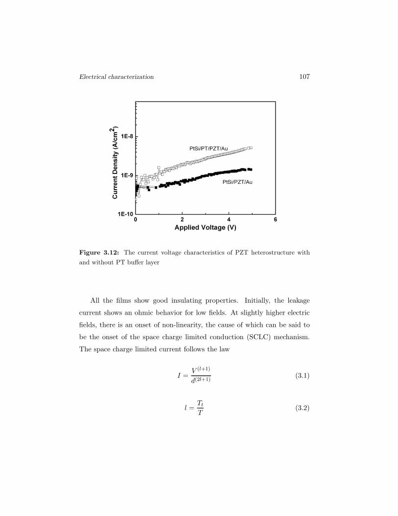
and voltage source. The figure 3.12 shows the leakage current density vs
electric field of PtSi/PZT/Au and PtSi/PT/PZT/Au structures. From the
figure it can be seen that the leakage current with PbTiO3 buffer layer is
greater than that of heterostructure with PZT thin film alone. The buffer
layer has not reduced the leakage current of PZT thin films in contrary
the leakage current has increased due to the buffer layer. The extrinsic
additives affect the nature and distribution of defects present in the PZT
thin films [108]. Defect distribution and their subsequent mobility have a
direct impact on leakage current. Oxygen defect of PZT thin films may
increase when PT thin films were used as buffer layer.At the same time
PZT thin films have the same structure as that of PT films. Hence leakage
current is of the same order [93].
Electrical characterization 107
Figure 3.12: The current voltage characteristics of PZT heterostructure with
and without PT buffer layer
All the films show good insulating properties. Initially, the leakage
current shows an ohmic behavior for low fields. At slightly higher electric
fields, there is an onset of non-linearity, the cause of which can be said to
be the onset of the space charge limited conduction (SCLC) mechanism.
The space charge limited current follows the law
I =V (l+1)
d(2l+1)(3.1)
l =Tt
T(3.2)
108 Pulsed laser deposition of PZT and PLZT
where, d = thickness of the thin films and Tt is the temperature param-
eter characterizing the trap distribution and T is the absolute temperature,
for a distributed-trap space-charge limited conduction[97]. The measure-
ment is carried out at room temperature. The conduction process for the
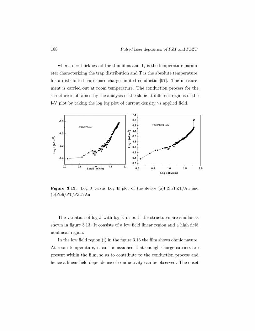
structure is obtained by the analysis of the slope at different regions of the
I-V plot by taking the log log plot of current density vs applied field.
Figure 3.13: Log J versus Log E plot of the device (a)PtSi/PZT/Au and
(b)PtSi/PT/PZT/Au
The variation of log J with log E in both the structures are similar as
shown in figure 3.13. It consists of a low field linear region and a high field
nonlinear region.
In the low field region (i) in the figure 3.13 the film shows ohmic nature.
At room temperature, it can be assumed that enough charge carriers are
present within the film, so as to contribute to the conduction process and
hence a linear field dependence of conductivity can be observed. The onset
Electrical characterization 109
of the non-linear character for both types of contacts lie within region(ii)
in the figure 3.13 , where a prominent role of the electrode is revealed.
The onset of non-linearity is a combined effect of the Schottky emission
through the contact interface and the SCLC mechanism within the bulk.
The leakage current in the films is dominated by space charge limited cur-
rent (SCLC) mechanism which can be expressed in the following form [109].
J =9µε0εrE
2
8d(3.3)
where J is the leakage current density, µ is the charge carrier mobility,
ε0 is the permitivity of free space,εr is the dielectric constant of the film
and d is the film thickness.
PtSi/ZnO/PZT/Au
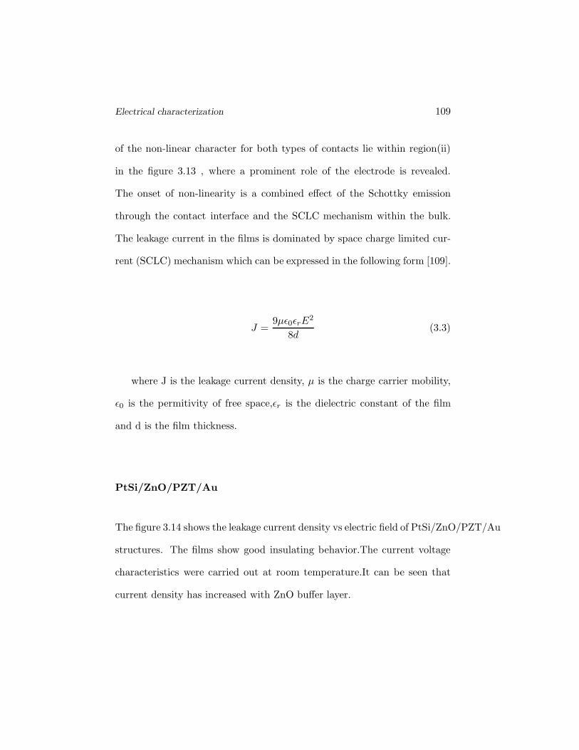
The figure 3.14 shows the leakage current density vs electric field of PtSi/ZnO/PZT/Au
structures. The films show good insulating behavior.The current voltage
characteristics were carried out at room temperature.It can be seen that
current density has increased with ZnO buffer layer.
110 Pulsed laser deposition of PZT and PLZT
Figure 3.14: The current voltage characteristics of the device
PtSi/ZnO/PZT/Au structure
The oxygen vacancies play an important role in the resistance degrada-
tion. They are positively charged with respect to the regular lattice and
thus in a dc electrical fields they migrate towards the cathode. The increase
in current density can be attributed to a decrease in the effective barrier
height at the cathode [110].
The applied voltage can be divided into two regions a low voltage region
and a high voltage region. The data is replotted according to equation for
Pool Frenkel emission as Log J/E vs E1/2 as shown in figure 3.15. The
log (J/E) curves show only a small increase with E1/2. In the high voltage
region these value increases linearly with E1/2.
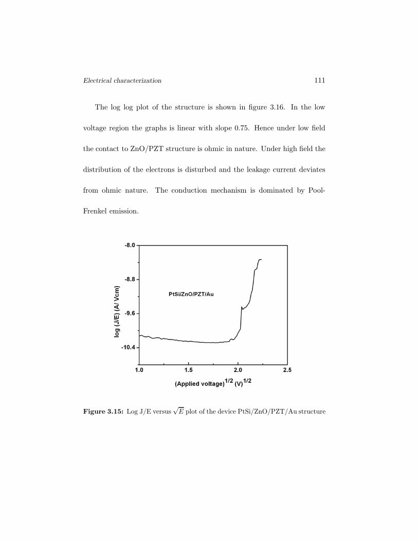
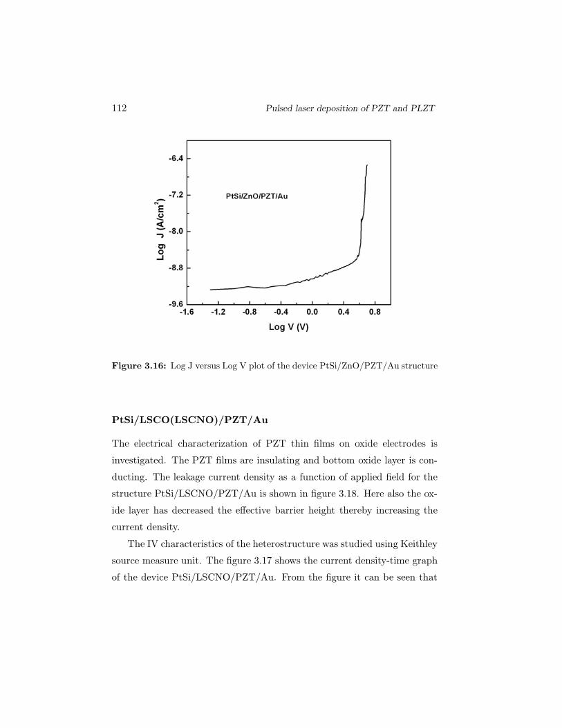
Electrical characterization 111
The log log plot of the structure is shown in figure 3.16. In the low
voltage region the graphs is linear with slope 0.75. Hence under low field
the contact to ZnO/PZT structure is ohmic in nature. Under high field the
distribution of the electrons is disturbed and the leakage current deviates
from ohmic nature. The conduction mechanism is dominated by Pool-
Frenkel emission.
Figure 3.15: Log J/E versus√
E plot of the device PtSi/ZnO/PZT/Au structure
112 Pulsed laser deposition of PZT and PLZT
Figure 3.16: Log J versus Log V plot of the device PtSi/ZnO/PZT/Au structure
PtSi/LSCO(LSCNO)/PZT/Au
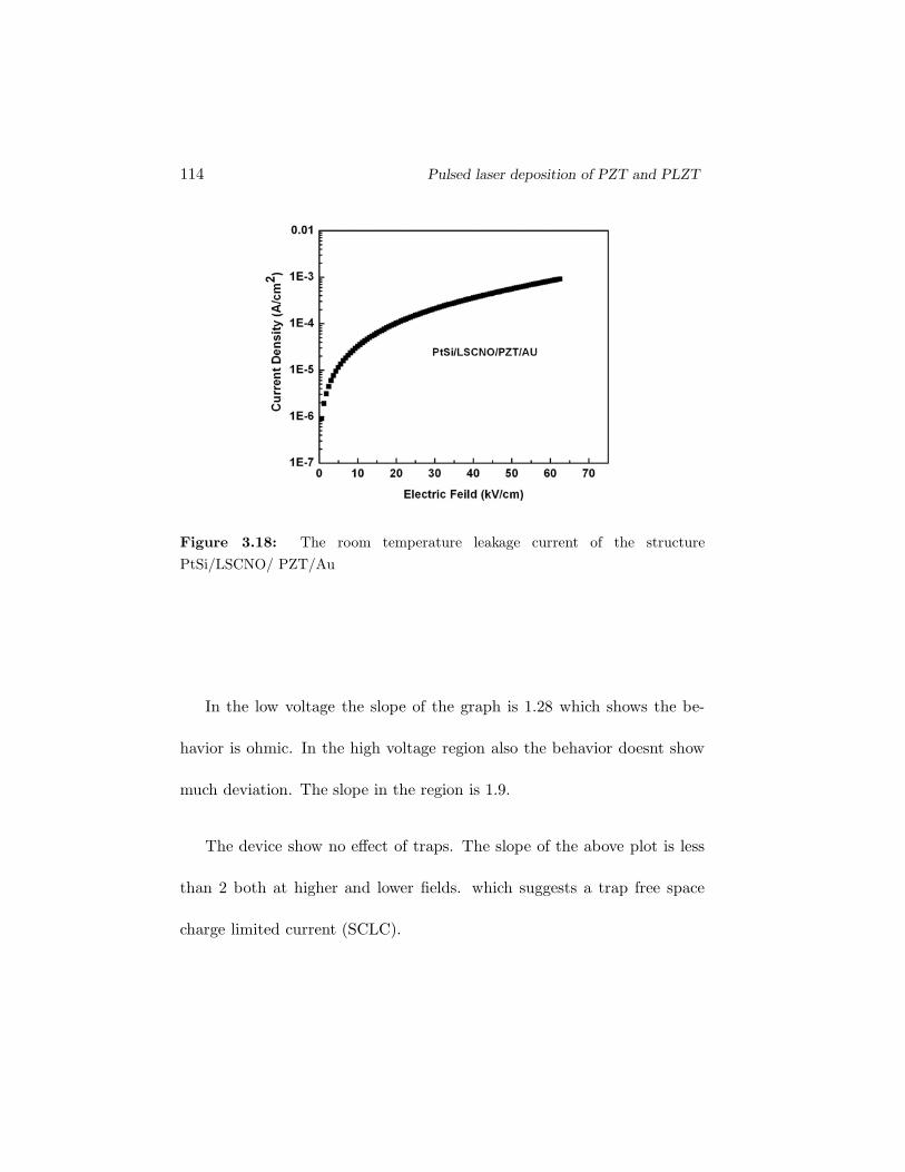
The electrical characterization of PZT thin films on oxide electrodes is
investigated. The PZT films are insulating and bottom oxide layer is con-
ducting. The leakage current density as a function of applied field for the
structure PtSi/LSCNO/PZT/Au is shown in figure 3.18. Here also the ox-
ide layer has decreased the effective barrier height thereby increasing the
current density.
The IV characteristics of the heterostructure was studied using Keithley
source measure unit. The figure 3.17 shows the current density-time graph
of the device PtSi/LSCNO/PZT/Au. From the figure it can be seen that
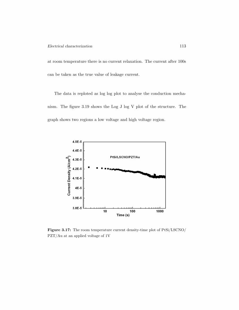
Electrical characterization 113
at room temperature there is no current relaxation. The current after 100s
can be taken as the true value of leakage current.
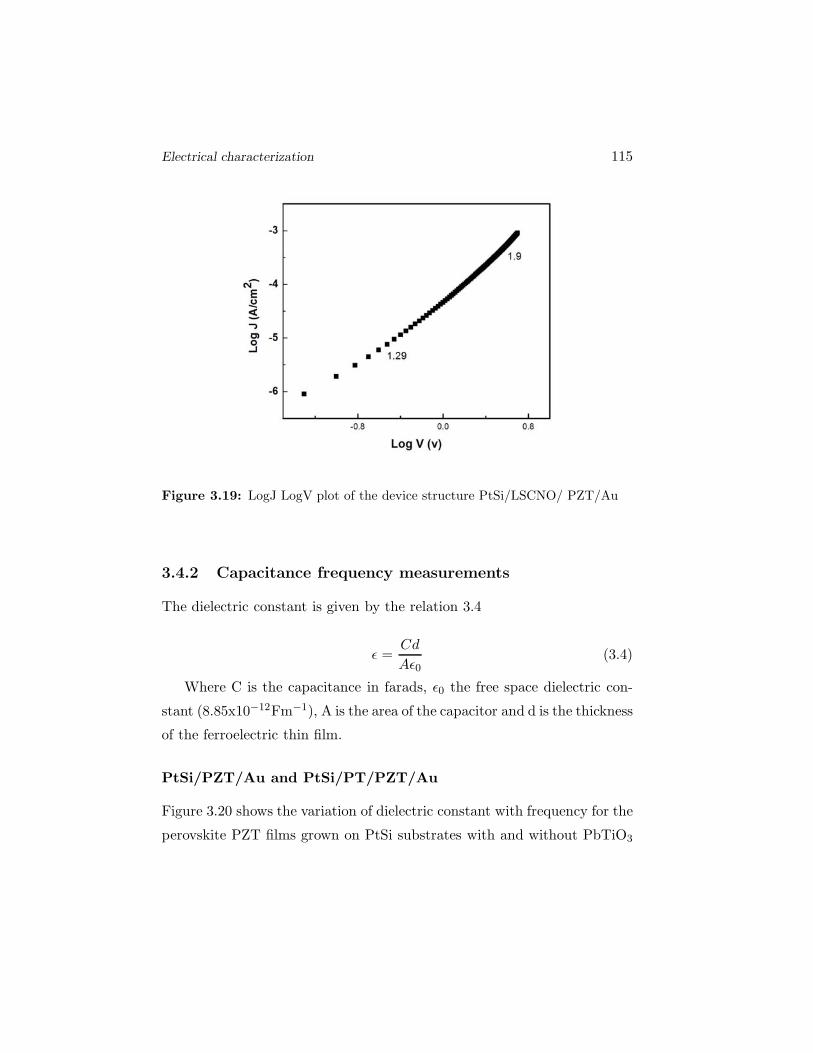
The data is reploted as log log plot to analyse the conduction mecha-
nism. The figure 3.19 shows the Log J log V plot of the structure. The
graph shows two regions a low voltage and high voltage region.
Figure 3.17: The room temperature current density-time plot of PtSi/LSCNO/
PZT/Au at an applied voltage of 1V
114 Pulsed laser deposition of PZT and PLZT
Figure 3.18: The room temperature leakage current of the structure
PtSi/LSCNO/ PZT/Au
In the low voltage the slope of the graph is 1.28 which shows the be-
havior is ohmic. In the high voltage region also the behavior doesnt show
much deviation. The slope in the region is 1.9.
The device show no effect of traps. The slope of the above plot is less
than 2 both at higher and lower fields. which suggests a trap free space
charge limited current (SCLC).
Electrical characterization 115
Figure 3.19: LogJ LogV plot of the device structure PtSi/LSCNO/ PZT/Au
3.4.2 Capacitance frequency measurements
The dielectric constant is given by the relation 3.4
ε =Cd
Aε0(3.4)
Where C is the capacitance in farads, ε0 the free space dielectric con-
stant (8.85x10⁻¹²Fm−1), A is the area of the capacitor and d is the thickness
of the ferroelectric thin film.
PtSi/PZT/Au and PtSi/PT/PZT/Au
Figure 3.20 shows the variation of dielectric constant with frequency for the
perovskite PZT films grown on PtSi substrates with and without PbTiO3
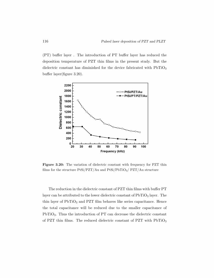
116 Pulsed laser deposition of PZT and PLZT
(PT) buffer layer . The introduction of PT buffer layer has reduced the
deposition temperature of PZT thin films in the present study. But the
dielectric constant has diminished for the device fabricated with PbTiO3
buffer layer(figure 3.20).
Figure 3.20: The variation of dielectric constant with frequency for PZT thin
films for the structure PtSi/PZT/Au and PtSi/PbTiO3/ PZT/Au structure
The reduction in the dielectric constant of PZT thin films with buffer PT
layer can be attributed to the lower dielectric constant of PbTiO3 layer. The
thin layer of PbTiO3 and PZT film behaves like series capacitance. Hence
the total capacitance will be reduced due to the smaller capacitance of
PbTiO3. Thus the introduction of PT can decrease the dielectric constant
of PZT thin films. The reduced dielectric constant of PZT with PbTiO3
Electrical characterization 117
finds application in pyroelectric detectors.
PtSi/ZnO/PZT/Au
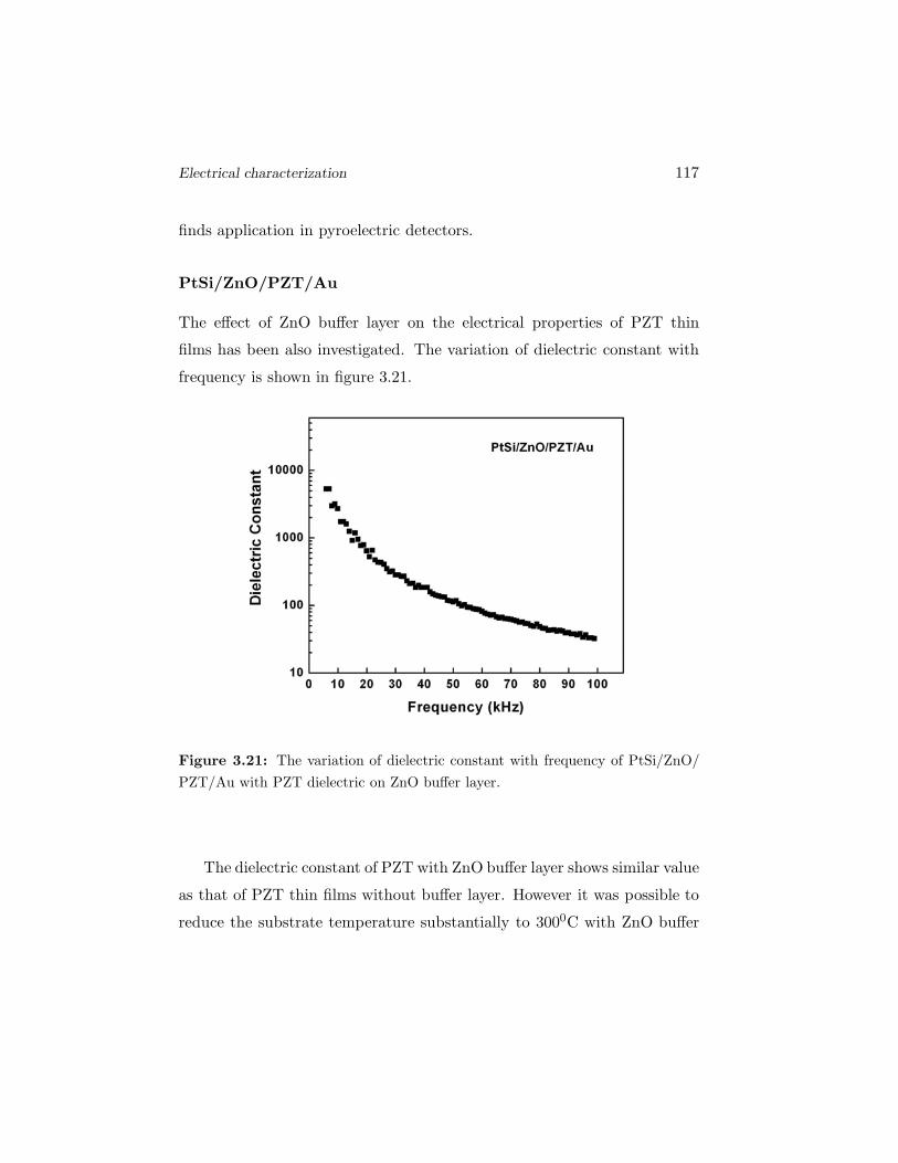
The effect of ZnO buffer layer on the electrical properties of PZT thin
films has been also investigated. The variation of dielectric constant with
frequency is shown in figure 3.21.
Figure 3.21: The variation of dielectric constant with frequency of PtSi/ZnO/
PZT/Au with PZT dielectric on ZnO buffer layer.
The dielectric constant of PZT with ZnO buffer layer shows similar value
as that of PZT thin films without buffer layer. However it was possible to
reduce the substrate temperature substantially to 3000C with ZnO buffer
118 Pulsed laser deposition of PZT and PLZT
layer.
ZnO buffer layer, a metal oxide, is known to contain oxygen vacancies
as a predominant point defects. It can alleviate the oxygen vacancy accu-
mulation at the PZT/ZnO interface via oxygen transport at the interface.
This should enhance the ferroelectric properties of PZT thin films. But in
the present work the orientation of PZT is along (101). The polarization
of the ferroelectric materials with the tetragonal structure is along (001)
direction [111].
PtSi/LSCNO/PZT/Au
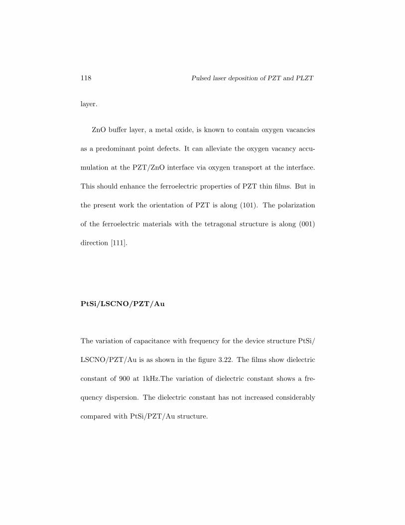
The variation of capacitance with frequency for the device structure PtSi/
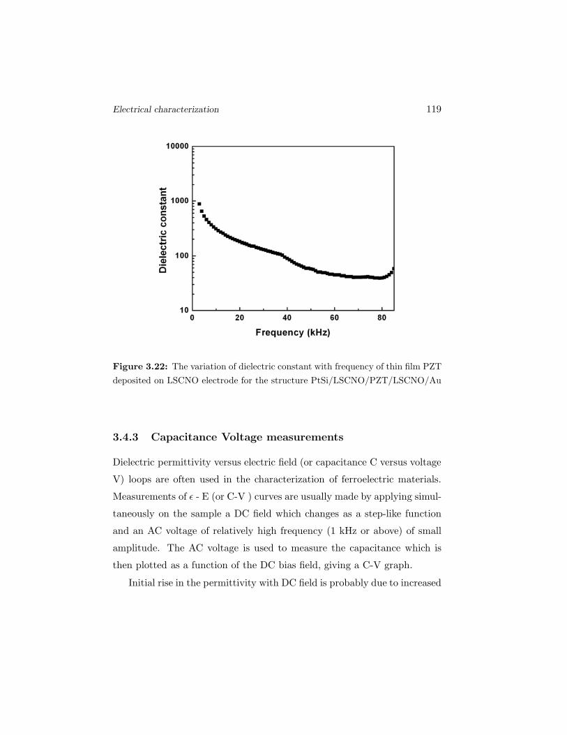
LSCNO/PZT/Au is as shown in the figure 3.22. The films show dielectric
constant of 900 at 1kHz.The variation of dielectric constant shows a fre-
quency dispersion. The dielectric constant has not increased considerably
compared with PtSi/PZT/Au structure.
Electrical characterization 119
Figure 3.22: The variation of dielectric constant with frequency of thin film PZT
deposited on LSCNO electrode for the structure PtSi/LSCNO/PZT/LSCNO/Au
3.4.3 Capacitance Voltage measurements
Dielectric permittivity versus electric field (or capacitance C versus voltage
V) loops are often used in the characterization of ferroelectric materials.
Measurements of ε - E (or C-V ) curves are usually made by applying simul-
taneously on the sample a DC field which changes as a step-like function
and an AC voltage of relatively high frequency (1 kHz or above) of small
amplitude. The AC voltage is used to measure the capacitance which is
then plotted as a function of the DC bias field, giving a C-V graph.
Initial rise in the permittivity with DC field is probably due to increased
120 Pulsed laser deposition of PZT and PLZT
movement of the domain walls which become ’free’ from defects and will
lock them at zero-DC field [112]. This is due to partial switching of some
domains whose coercive field happens to be small enough and which can
be switched by the DC and AC field combination. The maximum in the ε
- E curve appears in the vicinity of the coercive field for the P-E hysteresis
when most of the domains switch and the material appears to be dielectri-
cally very ’soft’. At high DC fields, the permittivity decrease reflects two
processes: (i) decrease in the number of domains as they become aligned
with the field (ideally the sample becomes a single domain and only lattice
contributions are present) and (ii) inhibition of the movement of residual
domain walls by the DC field [112].
In all the devices studied and presented in this chapter the top and
bottom electrode are of different material. The carrier concentration and
electronic work function of the top and bottom electrode are different.This
causes a shift in the C-V plot or hysteresis loop.
PtSi/PZT/Au
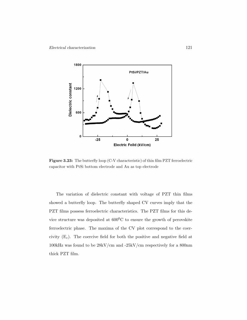
The variation of dielectric constant with voltage (ε - E) of PZT thin films
with PtSi as bottom and Au as top electrode is shown in figure below 3.23.
Electrical characterization 121
Figure 3.23: The butterfly loop (C-V characteristic) of thin film PZT ferroelectric
capacitor with PtSi bottom electrode and Au as top electrode
The variation of dielectric constant with voltage of PZT thin films
showed a butterfly loop. The butterfly shaped CV curves imply that the
PZT films possess ferroelectric characteristics. The PZT films for this de-
vice structure was deposited at 6000C to ensure the growth of perovskite
ferroelectric phase. The maxima of the CV plot correspond to the coer-
civity (Ec). The coercive field for both the positive and negative field at
100kHz was found to be 28kV/cm and -25kV/cm respectively for a 800nm
thick PZT film.
122 Pulsed laser deposition of PZT and PLZT
PtSi/PT/PZT/Au
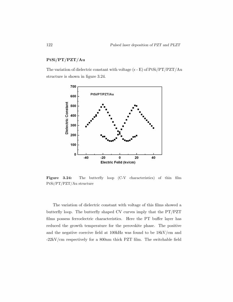
The variation of dielectric constant with voltage (ε - E) of PtSi/PT/PZT/Au
structure is shown in figure 3.24.
Figure 3.24: The butterfly loop (C-V characteristics) of thin film
PtSi/PT/PZT/Au structure
The variation of dielectric constant with voltage of this films showed a
butterfly loop. The butterfly shaped CV curves imply that the PT/PZT
films possess ferroelectric characteristics. Here the PT buffer layer has
reduced the growth temperature for the perovskite phase. The positive
and the negative coercive field at 100kHz was found to be 18kV/cm and
-22kV/cm respectively for a 800nm thick PZT film. The switchable field
Electrical characterization 123
of the device has also come down to 22kV/cm when PT buffer layer was
introduced.
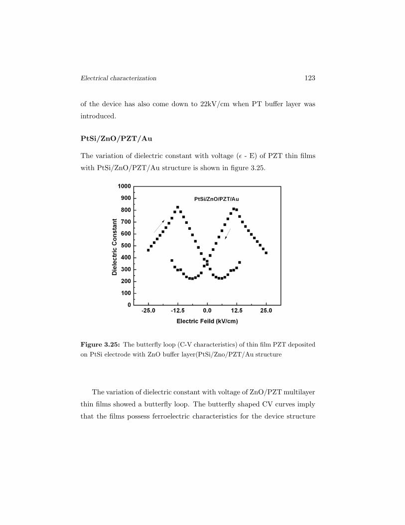
PtSi/ZnO/PZT/Au
The variation of dielectric constant with voltage (ε - E) of PZT thin films
with PtSi/ZnO/PZT/Au structure is shown in figure 3.25.
Figure 3.25: The butterfly loop (C-V characteristics) of thin film PZT deposited
on PtSi electrode with ZnO buffer layer(PtSi/Zno/PZT/Au structure
The variation of dielectric constant with voltage of ZnO/PZT multilayer
thin films showed a butterfly loop. The butterfly shaped CV curves imply
that the films possess ferroelectric characteristics for the device structure
124 Pulsed laser deposition of PZT and PLZT
PtSi/ZnO/PZT/Au. The ZnO layer has substantially reduced the growth
temperature of PZT thin films to 3000C. But the ferroelectric properties
were not deteriorated with the ZnO buffer layer. The maxima of the CV
plot correspond to the coercivity (Ec). The coercive field at 100kHz was
found to be 12kV/cm -15.6kV/cm for a 800nm thick PZT film. The switch-
able field of PtSi/ZnO/PZT/Au is smaller than that of PtSi/PT/PZT/Au
structure.
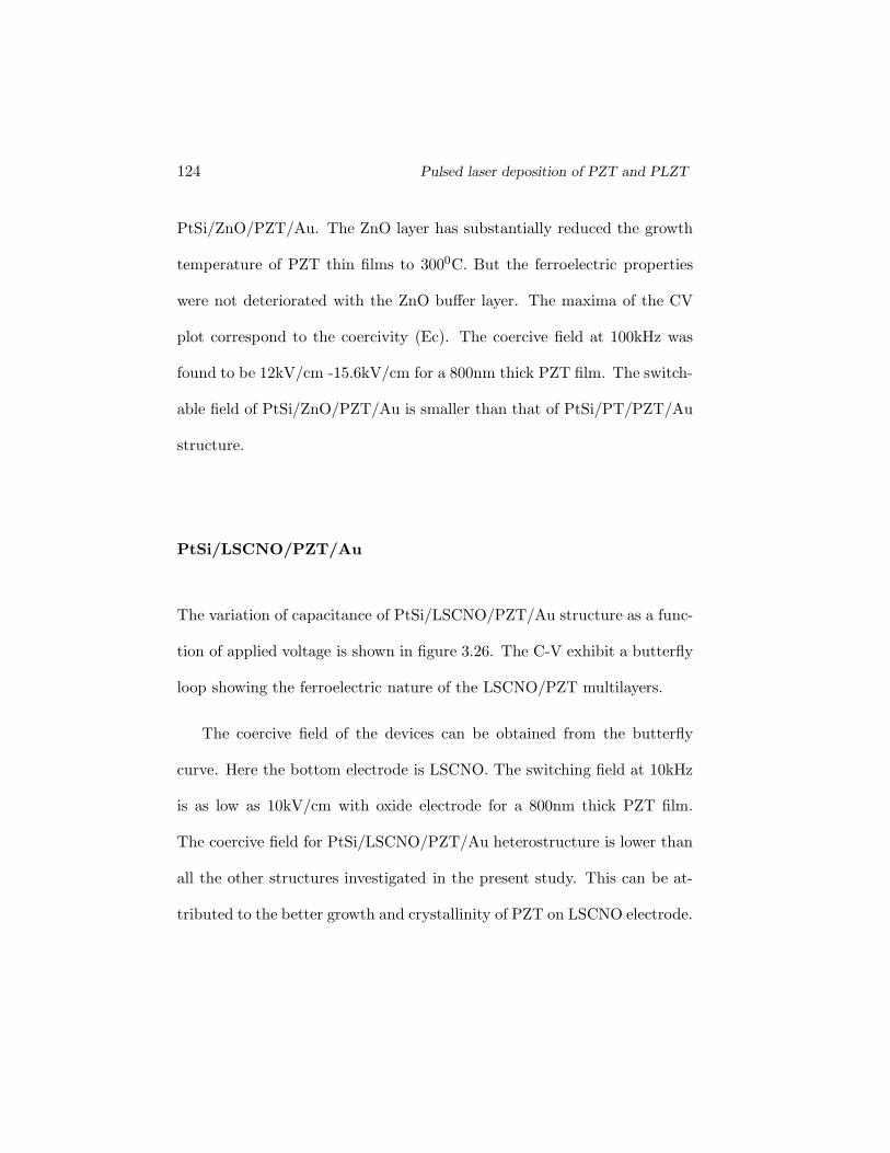
PtSi/LSCNO/PZT/Au
The variation of capacitance of PtSi/LSCNO/PZT/Au structure as a func-
tion of applied voltage is shown in figure 3.26. The C-V exhibit a butterfly
loop showing the ferroelectric nature of the LSCNO/PZT multilayers.
The coercive field of the devices can be obtained from the butterfly
curve. Here the bottom electrode is LSCNO. The switching field at 10kHz
is as low as 10kV/cm with oxide electrode for a 800nm thick PZT film.
The coercive field for PtSi/LSCNO/PZT/Au heterostructure is lower than
all the other structures investigated in the present study. This can be at-
tributed to the better growth and crystallinity of PZT on LSCNO electrode.
Electrical characterization 125
Figure 3.26: The butterfly loop (C-V characteristics) for PtSi/LSCNO/PZT/Au
device
The LSCNO being an oxide electrode compensate the oxygen vacancy
accumulation at the PZT/LSCNO interface. This may improve the ferro-
electric property since oxygen vacancy play a detrimental role in domain
wall pinning which was widely accepted as the main mechanism of ferro-
electric fatigue.
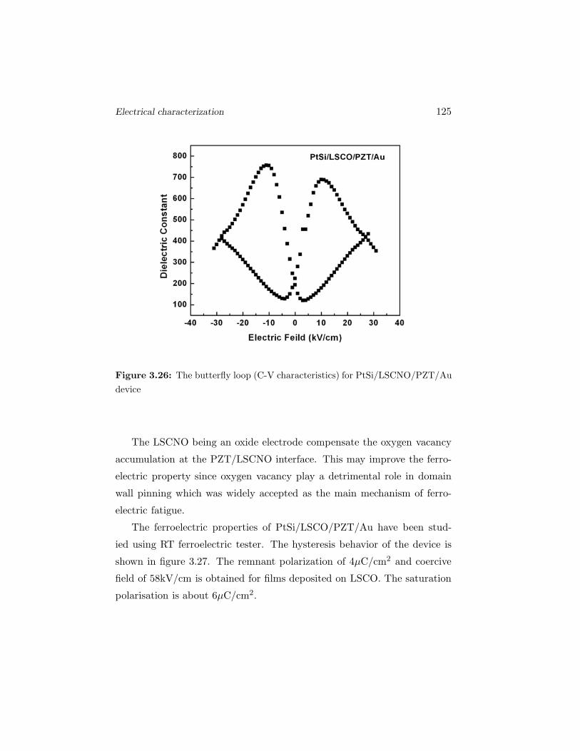
The ferroelectric properties of PtSi/LSCO/PZT/Au have been stud-
ied using RT ferroelectric tester. The hysteresis behavior of the device is
shown in figure 3.27. The remnant polarization of 4µC/cm2 and coercive
field of 58kV/cm is obtained for films deposited on LSCO. The saturation
polarisation is about 6µC/cm2.
126 Pulsed laser deposition of PZT and PLZT
Figure 3.27: P-E hysteresis loop of the PtSi/LSCO/PZT/Au structure
3.5 Conclusion
PZT and PLZT thin films were deposited by pulsed laser deposition on
PtSi substrates. Pure perovskite phase PZT thin films was obtained at a
substrate temperature 6000C for PZT thin films. The Pb excess targets
were used for compensating the Pb loss in the PZT thin films. PbTiO3 and
ZnO buffer layers were deposited to lower the deposition temperature. Per-
voskite phase was formed in all thin films at much lower temperature.The
PT buffer layer have decreased the dielectric constant of PZT thin films for
Conclusion 127
possible application in pyroelectric detectors. ZnO buffer layer has lowered
the deposition temperature to 3000C. Stoichiometry is confirmed by com-
position analysis of the samples. Electrical characterization of the samples
with and without buffer layer were studied. The leakage current through
the sample were studied. The variation of dielectric constant with fre-
quency shows a dispersion nature.The capacitance voltage measurements
show butterfly loop for all the ferroelectric samples. The coercive field of
the structure is the maxima of the C-V plot.This switchable field is lower
for films deposited with LSCNO oxide electrode.
128 Pulsed laser deposition of PZT and PLZT
Recommended


![Respiration (PZT) Sensor Data Sheet - BITalinobitalino.com/datasheets/PZT_Sensor_Datasheet.pdfRespiration (PZT) Sensor Data Sheet ! PAGE 2 OF 2 !!! TRANSFER FUNCTION [-50%, 50%] !"#%=!"#](https://img.pdfslide.us/doc/110x75/5abe1d507f8b9a7e418c7f97/respiration-pzt-sensor-data-sheet-pzt-sensor-data-sheet-page-2-of-2-.jpg)