Yu-Lin Wang
Department of Materials Science and Engineering , University of Florida
Oxide-based Electric Devices :Oxide-based Electric Devices :
Flexible Transparent Thin Film TransistorsFlexible Transparent Thin Film Transistors

Background
Soldiers can use flexible display computers on the battlefield for communication and information access.
Flexible displays are attractive for portable devices such as cell phone, PDA, laptop, e-book and wearable due to their lightweight, low power consumption, and being bendable.

Flexible display
Currently, these display either use a-Si TFTs or organic TFTs (OTFTs) in the active matrix arrays.
To get a high resolution display, high mobility TFTs are necessary. However, a-Si TFTs or OTFTs cannot fit this application.

Material Comparisons
Which material is a better choice for the transparent and flexible display?
IZO : Indium znic oxide

1. High transparency : available for transparent TFTs
2. Room temperature process : available for plastics substrate
3. Can be used as electrodes, or channel layers : by adjusting O2 ratio
4. High field effect mobility : 10 ~ 50 cm2V-1S-1
5. Large area deposition : By sputtering machine
6. Rapid Process
7. Low cost
Advantages of the IZO Thin Film Transistors
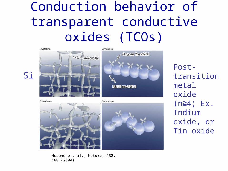
Conduction behavior of transparent conductive oxides (TCOs)
Hosono et. al., Nature, 432, 488 (2004)
SiPost-transition metal oxide (n 4) Ex. ≧Indium oxide, or Tin oxide
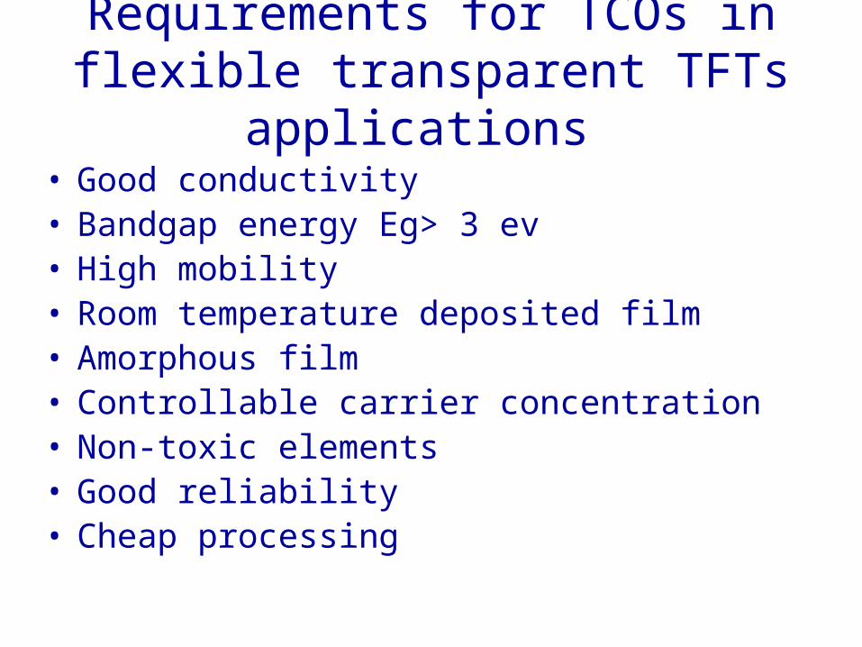
Requirements for TCOs in flexible transparent TFTs applications
• Good conductivity• Bandgap energy Eg> 3 ev• High mobility• Room temperature deposited film • Amorphous film• Controllable carrier concentration• Non-toxic elements• Good reliability • Cheap processing

Various conductive oxides

TFTs on flexible substrates
1. Directly deposit film on flexible substrates (plastics) and fabricate TFTs.
2. Fabricate TFTs on hard substrate (glass) and then transfer the TFTs to flexible substrates (plastics).
Currently, most TFTs use α-Si or organic TFTs (OTFTs). Two methods are used to fabricate these TFTs on flexible substrates.

InGaZnO TFTs on PETPET : polyethylene terephthalate
Threshold voltage 1.3V
On/Off ratio > 105
Sub-threshold voltage swing ~0.24 V/decade
Field effect mobility ~10 cm2V-1S-1
gm ~0.03 mS/mm Hosono et. al., Jpn, J. Appl. Phys., 45, 4303 (2006)

By choosing different oxygen ratio, we can choose what carrier concentration we need
0.0 0.5 1.0 1.5 2.0 2.5 3.0 3.51x10¹³
1x10¹⁵
1x10¹⁷
1x10¹⁹
1x10²¹
1x10²³
C
arri
er C
once
ntr
atio
n (
cm-3)
% O2 in O
2 + Ar [%]
Carrier concentration
0
10
20
30
40
50
60R
esistivity (ohm
-cm)
125W-ZnO 150W-In2O
3
5 mTorr chamber pressure
Carrier mobility
Carrier M
obility (cm
2/V-sec.)
Resistivity
IZO Film : Oxygen Ratio Dependence

Depletion mode TFTs
Fabricated
Channel : IZO
Gate dielectrics : SiO2, SiNx
Plan to do
Channel : IZO or IGZO or SIZO
Gate dielectrics : SiO2, SiNx, Sc2O3

Process sequences

Enhancement mode TFTs
Fabricated
Channel : IZO
Gate dielectrics : SiO2
Plan to do
Channel : IZO or IGZO or SIZO
Gate dielectrics : SiO2, SiNx, Sc2O3

Large Area Depletion Mode TFTs
IZO film : Carrier concentration ~1018 cm-3
Gate Width/Length =100um / 36umG
S
D
Source
Gate
Drain
SiO2 SiO2
Glass Substrate
SiO2 50nm
IZO 50 nm
Pt 20nm
Au 80nm
Au 80nmTi 20nm Ti 20nm
Au 80nm

0 1 2 3 4 50.00
0.05
0.10
0.15
0.20
0.25
Step= -1V
Vg= 0V
Gate W/L: 100 m / 36 m
Dra
in-S
ourc
e C
urr
ent
(mA
)
Drain-Source Voltage (V)
Large Area Depletion Mode TFT Performance
-9 -8 -7 -6 -5 -4 -3 -2 -1 00.000
0.002
0.004
0.006
0.008
0.010
0.012
0.014
dsI
Gate W/L: 100 m / 36 m
Dra
in-S
ourc
e C
urr
ent
(A1/
2 )
Gate Voltage (V)
0.0
0.1
0.2
0.3
0.4
0.5
0.6
0.7
0.8
mg
Ext
r. T
ran
scon
du
ctan
ce (
mS
/mm
)
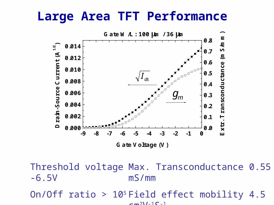
Max. Transconductance 0.55 mS/mm
Field effect mobility 4.5 cm2V-1S-1
Threshold voltage -6.5V
On/Off ratio > 105
Large Area TFT Performance

-3 -2 -1 0 1 2 30
1x10⁻¹⁰
2x10⁻¹⁰
3x10⁻¹⁰
4x10⁻¹⁰
5x10⁻¹⁰Gate W/L: 100 m X 36 m
Gat
e C
urr
ent
(A)
Gate Voltage (V)
Gate dielectric: SiO2 50 nm
Gate Dielectric Leakage
Gate leakage current ~ 10-10 A

Small Gate length Depletion Mode TFTs
IZO film : Carrier concentration ~1018 cm-3
Gate W/L =200um / 1um
Gate dielectric : SiNx 12.5 nm
Pt 20nmAu 80nm
IZO 50nm
Au 80nm
Ti 20nm Ti 20nm
Au 80nm
SiNx 12.5nm
Glass


0 1 2 3 4 50.00.20.40.60.81.01.21.41.61.8
Gate W/L=200 m/1 m
Vg= 0V
Step= -0.5V
Drain-Source Voltage (V)
Dra
in-S
ourc
e C
urr
ent
(mA
)
Small Gate length Depletion Mode TFT Performance

Max. Transconductance 7.5 mS/mm
Field effect mobility 14.5 cm2V-1S-1
Threshold voltage -2.5V
On/Off ratio > 105
-6 -5 -4 -3 -2 -1 0 10.00
0.01
0.02
0.03
0.04
0.05Gate W/L= 200m/1m
mgdsI
Dra
in-S
ourc
e C
urr
ent
(A1/
2 )
Gate Voltage (V)
0
2
4
6
8
10
Ext
r. T
ran
scon
du
ctan
ce (
mS
/mm
)
Small Gate length TFT Performance
10 1000
2
4
6
8
10
12
fT
fmax
Gai
n (
dB
)
Frequency (MHz)
U
h21
h21
U
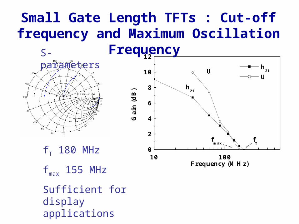
Small Gate Length TFTs : Cut-off frequency and Maximum Oscillation Frequency
fT 180 MHz
fmax 155 MHz
Sufficient for display applications
S-parameters

Small Gate length Enhancement Mode TFTs
IZO film : Carrier concentration ~1x1016 cm-3
Gate W/L =100um / 1um
Gate dielectric : SiO2 100 nm

Enhancement Mode TFT : Ids vs. Vds

Enhancement Mode TFT Performance
Threshold voltage 0.5V
On/Off ratio ~ 105Max. Transconductance ~10 mS/mm
Sub-threshold voltage swing ~0.135 V/decade
SummaryVery high performance depletion mode and enhancement mode TFTs were achieved on glass substrates.
Very good frequency response from a depletion mode TFT which is very sufficient for display applications.
IZO and IGZO will be used as channel layers to fabricate depletion mode and enhancement mode TFTs and ring oscillators on glass and flexible transparent substrate (PET).
The SiO2-In2O3-ZnO system and N2 plasma incorporated IZO film will be grown to get a better controllability of the carrier concentration.
Recommended