Optimum Luminescent Down-Shifting
Properties for High Efficiency and Stable
Perovskite Solar Cells
Miguel Alexandre*, Manuel Chapa, Sirazul Haque, Manuel J. Mendes*,
Hugo Águas, Elvira Fortunato, Rodrigo Martins
I3N/CENIMAT, Department of Materials Science, Faculty of Science and Technology,
Universidade NOVA de Lisboa and CEMOP/UNINOVA, Campus de Caparica, 2829-516
Caparica, Portugal
*Corresponding author: [email protected], [email protected]
Abstract
In recent years, the discovery of the excellent optical and electrical properties of
perovskite solar cells (PSCs) made them a main focus of research in photovoltaics,
with efficiency records increasing astonishingly fast since their inception. However,
problems associated with the stability of these devices are hindering their market
application. UV degradation is one of the most severe issues, chiefly caused by TiO2’s
photo-generated electrons that decompose the perovskite absorber material, coupled
with the additional intrinsic degradation of this material under UV exposure. The
solution presented here can minimize this effect while boosting the cells’ generated
photocurrent, by making use of combined light-trapping and luminescent down-
shifting effects capable of changing the harmful UV radiation to higher wavelengths
that do not affect the stability and can be effectively “trapped” in the cell. This work
focuses in the optimization of the photocurrent gains that can be attained by
emulating the changed spectrum resulting from applying down-shifting media as
encapsulant in photonic-enhanced PSCs, as well as the reduction in the harmful
effects of UV radiation on the devices. Such optimized photonic solution allows
current enhancement while reducing the harmful UV photo-carrier generation both in
the TiO2 (by one order of magnitude) and in the perovskite (by 80%) relative to a
standard PSC without light management.
Keywords: Photonics, Perovskite Solar Cells, Luminescent Down-shifting, UV
Stability, Photocurrent Enhancement
1
1. Introduction
The ever-growing cost-competitiveness of photovoltaic (PV) technology is the
main reason behind the recent growth in total global PV installed capacity (increasing
from under 50 GW to above 400 GW from 2010 to 2017).1–3 Crystalline silicon (c-Si)
solar cells have been the uncontested market leaders of this technology.2,4 However,
the need to keep fueling this growth has turned the researchers’ attention to other
materials and light management techniques, as the sub-optimal absorption of c-Si is
an obstacle in a scenario of ever-decreasing material thickness,5,6 which is a
fundamental factor for low cost and flexible photovoltaics.7,8 Therefore, novel
materials with excellent optical properties have been studied to achieve lower
thickness without imperiling the device’s performance. The class of materials that, in
recent years, has stood out from the rest are hybrid organic-inorganic perovskites
(HOIPs), as they exhibit direct bandgap,9–11 long carrier diffusion lengths,12,13 and
high optical absorption coefficient.11,12,14 The evidenced properties paved the way for
the fast adoption of these materials, thus leading to a steep increase in PV conversion
efficiency reaching values above 22% in just a few years.9,13,15–17 HOIPs are based
on an ABX3 atomic structure, where A and B are cations of different size and X is an
anion.9,18 The first is an organic or inorganic ion (methylammonium, CH3NH3+;
ethylammonium, CH3CH2NH3+; formamidinium, NH2CH=NH2
+, Cs and Rb), the
second a divalent metal cation (Ge2+, Sn2+ and Pb2+). The last element on the
structure, X, is a monovalent halogen anion (F-, Cl-, Br-, I-).9,12,18
Although perovskite solar cells (PSCs) display an impressive performance,
competing with the best silicon solar cells in terms of efficiency, they have several
stability problems mainly related with exposure to moisture, oxygen and UV
radiation, that are responsible for blocking its market implementation.18 These
degradation mechanisms are not yet fully understood, however several studies have
defined many possible mechanisms.19–21 Moisture and oxygen exposure can be
mostly prevented via proper encapsulation,21 leaving UV exposure as the most
important susceptibility to overcome. The UV degradation of PSCs has been attributed
to photocatalytic effects caused by TiO2, the material commonly used as electron
transport layer (ETL). This effect was first reported by Leijtens et. al. where it was
hypothesized that, upon electron excitation in TiO2, deep trap states are created that
capture photo-electrons generated in the absorber material, therefore hindering the
cell’s performance.22 Ito et. al. also suggested that the formation of I2, due to electron
transfer to deep trap states in the TiO2/perovskite interface, can then decompose the
perovskite crystal by evaporation of volatile compounds.20 Regarding perovskite
2
degradation, excluding the TiO2’s effects, Quistch et. al. calculated the threshold
energy between the perovskite’s photo-brightening and photo-degradation,
correlating it with the presence of residual PbI2. This study indicated that I2 can be
created by the photolysis of PbI2, leading to an equivalent degradation process to the
aforementioned one.23
Considering the above-mentioned problems, several techniques have been used
to mitigate these degradation mechanisms, such as replacing TiO2 by other non-
harmful materials,22 depositing blocking layers between the TiO2/perovskite interface
to avoid electron exchange,20 as well as the use of either a UV filter or a down-shifting
(DS) layer that prevents UV radiation from reaching the cell.22,24–26 This latter case is
the one that was unprecedentedly optimized in this study.
Down-shifting is the process where high energy photons are converted to lower
energy photons.27,28 The main materials used for this process are quantum dots
(QDs),29–32 dyes 33–35 and rare-earth elements.36–38 These materials have recently
been applied to perovskite,25,26 organic39 and dye sensitized solar cells40 to improve
their life-time without compromising their overall performance. When compared with
the use of UV filters, which is the current common way of enhancing the UV stability
of PSCs,22 using DS benefits from the exploitation of the energy of otherwise lost
photons, while still protecting the absorber material from the harmful UV radiation.
One example, by Anizelli et. al., compared the results against a UV filter obtaining a
similar development of the device’s parameters with prolonged UV exposure.25
As stated earlier, the need for ever-decreasing thickness without compromising
solar cell performance is a driver for research in the PV field. However, decreasing
thickness leads to lower red-NIR absorption, as this radiation has higher penetration
depth. Therefore, different light-trapping (LT) methods have been studied to improve
this low-energy absorption, such as the use of metallic or dielectric nanoparticles,41–
43 front or rear texturing of the cell6,44,45 and the use of high index dielectric structures
on the cell front.7,46,47 This latter LT method, operating in the regime of wave-optics,
is the one considered in this work. Front-located high index photonic structures allow
strong forward scattering of light, thus increasing its travel path within the PV
absorber, as well as the creation of resonant modes, related with the structure’s
properties, that can greatly boost the cell’s absorption. For periodic structures, this
increase can even surpass the theoretical limit – the Tiedje-Yablonovitch limit – for
specific wavelengths related with the LT structure’s pitch.6,47,48
3
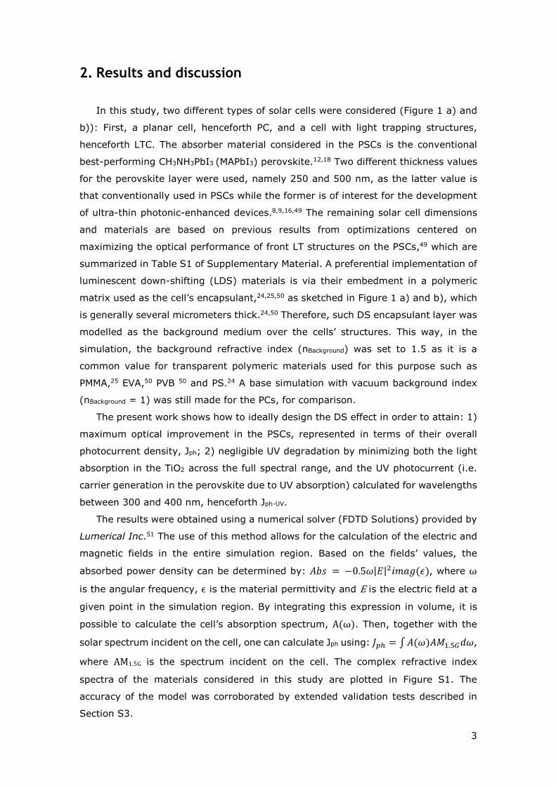
2. Results and discussion
In this study, two different types of solar cells were considered (Figure 1 a) and
b)): First, a planar cell, henceforth PC, and a cell with light trapping structures,
henceforth LTC. The absorber material considered in the PSCs is the conventional
best-performing CH3NH3PbI3 (MAPbI3) perovskite.12,18 Two different thickness values
for the perovskite layer were used, namely 250 and 500 nm, as the latter value is
that conventionally used in PSCs while the former is of interest for the development
of ultra-thin photonic-enhanced devices.8,9,16,49 The remaining solar cell dimensions
and materials are based on previous results from optimizations centered on
maximizing the optical performance of front LT structures on the PSCs,49 which are
summarized in Table S1 of Supplementary Material. A preferential implementation of
luminescent down-shifting (LDS) materials is via their embedment in a polymeric
matrix used as the cell’s encapsulant,24,25,50 as sketched in Figure 1 a) and b), which
is generally several micrometers thick.24,50 Therefore, such DS encapsulant layer was
modelled as the background medium over the cells’ structures. This way, in the
simulation, the background refractive index (nBackground) was set to 1.5 as it is a
common value for transparent polymeric materials used for this purpose such as
PMMA,25 EVA,50 PVB 50 and PS.24 A base simulation with vacuum background index
(nBackground = 1) was still made for the PCs, for comparison.
The present work shows how to ideally design the DS effect in order to attain: 1)
maximum optical improvement in the PSCs, represented in terms of their overall
photocurrent density, Jph; 2) negligible UV degradation by minimizing both the light
absorption in the TiO2 across the full spectral range, and the UV photocurrent (i.e.
carrier generation in the perovskite due to UV absorption) calculated for wavelengths
between 300 and 400 nm, henceforth Jph-UV.
The results were obtained using a numerical solver (FDTD Solutions) provided by
Lumerical Inc.51 The use of this method allows for the calculation of the electric and
magnetic fields in the entire simulation region. Based on the fields’ values, the
absorbed power density can be determined by: , where
is the angular frequency, is the material permittivity and is the electric field at a
given point in the simulation region. By integrating this expression in volume, it is
possible to calculate the cell’s absorption spectrum, . Then, together with the
solar spectrum incident on the cell, one can calculate Jph using: ,
where is the spectrum incident on the cell. The complex refractive index
spectra of the materials considered in this study are plotted in Figure S1. The
accuracy of the model was corroborated by extended validation tests described in
Section S3.
4
Figure 1 - Schematic of the solar cell structures considered in the simulations. a) Planar
cell structure used as reference, composed by the layers: Metal contact (Ag)/Hole Transport
Layer (HTL, made of Spiro-OMeTAD)/Absorber (Perovskite)/ Electron Transport Layer (ETL,
made of TiO2), Transparent conductive oxide (TCO, made of ITO). b) Light trapping cell
structures integrated in the n-contact (ETL) of the PSC. The corresponding cell dimensions are
shown in Supplementary Material - Table S1. c) Plot illustrating the method used to emulate
the process of down-shifting. In dashed green is the gaussian profile, in blue is the absorbed
flux and in red is the emitted flux; d) schematic depicting the process of down-shifting by an
LDS material.
Since this is an electromagnetic method based on Maxwell’s equations, it cannot
exactly simulate the effect of DS. Consequently, here DS was modelled by proper
adaptation of the incident spectrum, as described in Figure 1 c). Based on absorption
and emission profiles of typical LDS materials, taken from several reports,25,33,35,39,52–
54 a gaussian profile was chosen to emulate these properties - Figure 1 c) green
dashed profile. Gaussian profiles have three main variables: the gaussian RMS width,
parameter related with the FWHM which was fixed at 50 nm; the gaussian center, ,
that was left as a variable; and the amplitude, representing the peak absorption, that
was fixed at unity. This gaussian absorption was then multiplied with the solar photon
5
flux, based on the ASTM G-173 global irradiance spectra provided by NREL,55 to
calculate the hypothetical absorption flux in a thick DS layer - Figure 1 c) blue profile.
Subsequently, this absorbed flux is shifted to higher wavelengths, as shown in Figure
1 c), by a shifting parameter, , that was also left as a variable. Lastly, to create
the “shifted” spectrum incident on the PSC, the absorbed flux was subtracted, while
the emission flux was added to the pristine AM1.5G spectrum. As an example, Figure
S2 shows the resulting spectral irradiance plots for two different and . It should
be noted that the process used to emulate the DS process is an ideal one and, thus,
does not account for effects such as isotropic emission, non-unitary quantum
efficiency and reabsorption.
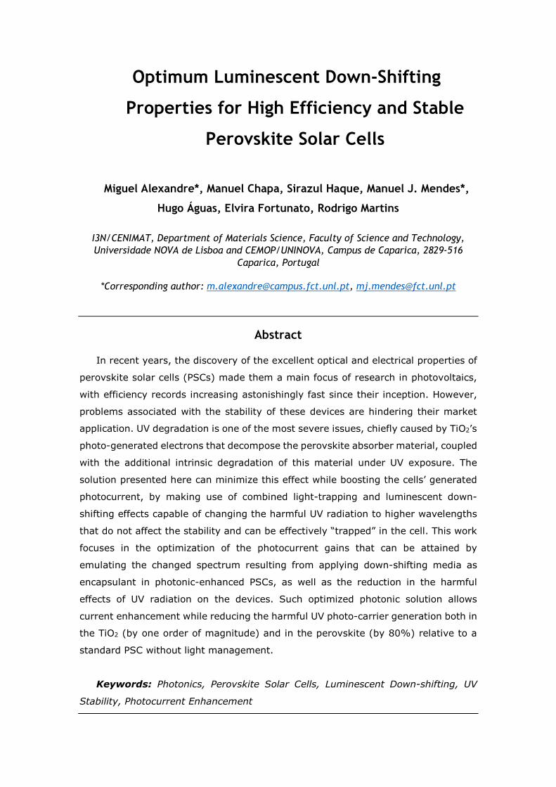
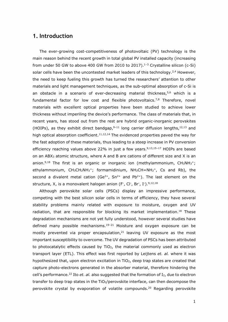
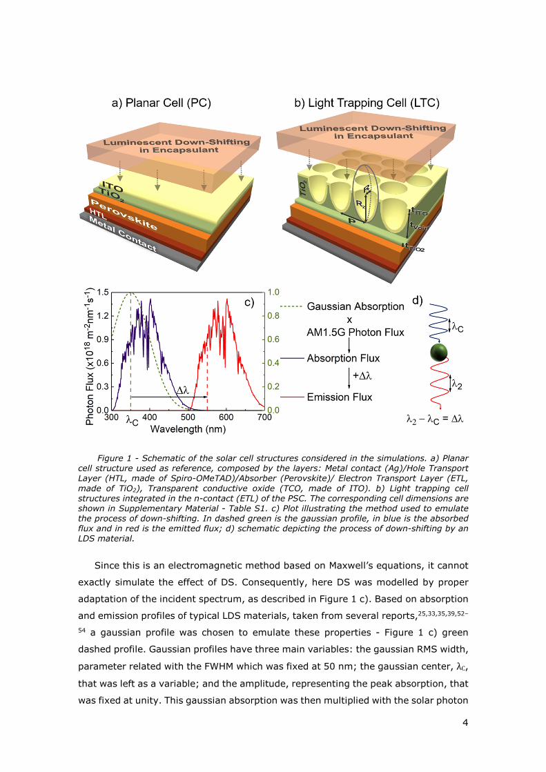
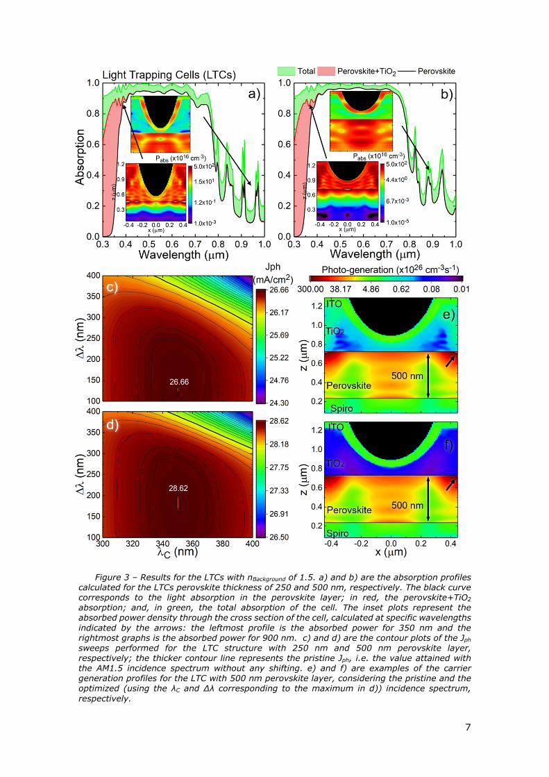
Firstly, the solar cells’ absorption profiles were determined by the aforementioned
method and are displayed in Figure 2 a) and b) for the PCs and in Figure 3 a) and b)
for the LTCs, considering the nBackground = 1.5. The profiles for nBackground = 1.0 are
shown in Section S4 of Supplementary Material. These absorption profiles only
depend on the solar cells’ structure and materials, being independent of the
illumination spectrum. Therefore, they are suited to evaluate the device’s optical
performance. For red-NIR wavelengths there is a decrease in the cell absorption as
sub-bandgap photons are harder to absorb. This is effectively shown by the absorbed
power density plots shown for 900 nm wavelength (rightmost inset profiles in Figure
2 and Figure 3), as the absorption is rather uniform throughout the cell. Note that,
for the LTCs, these losses are reduced by the use of the photonic structures
responsible for scattering light. For shorter wavelengths, the most notable aspect is
the parasitic absorption from TiO2 and ITO for both PCs and LTCs. The absorbed
power density plots (leftmost inset plots in Figure 2 and Figure 3 at 350 nm
wavelength) again serve to further verify this statement, as they show a pronounced
absorption in the TiO2 and ITO layers. Furthermore, the LTCs show an effective UV
shading of the perovskite, revealed by the red shaded area in the absorption spectra
of Figure 3 a) and b) as well as the substantial absorbed power density in the front
LT structures shown by the 350 nm inset profiles in Figure 3. This increase is due to
the thick TiO2 used in these structures, as it is the material responsible for the light
trapping effects (i.e. improved broadband anti-reflection and scattering).49 It should
be noted that such UV shading is also beneficial for the perovskite cells, due to the
UV instability problems.
Subsequently, sweeps were made for the different cells in study, where and
where varied between 100-400 nm and 300-400 nm, respectively. The resulting
photocurrent contour plots for the PCs are shown in Figure 2 c) and d), and for the
LTCs in Figure 3 c) and d). The equivalent results for the PCs with nBackground = 1 are
shown in Section S5.
6
Figure 2 – Results for the PCs structure with nBackground of 1.5. a) and b) are the absorption
profiles calculated for the PCs with perovskite thickness of 250 and 500 nm, respectively. The
black curve corresponds to the light absorption in the perovskite layer; in red, the
perovskite+TiO2 absorption; and, in green, the total absorption of the cell. The inset plots
represent the absorbed power density through the cross section of the cell, calculated at
specific wavelengths indicated by the arrows: the leftmost profile is the absorbed power for
350 nm and the rightmost graph is the absorbed power for 900 nm; c) and d) are the contour
plots of the photocurrent density (Jph) sweeps performed for the PC structure with 250 nm and
500 nm perovskite layer, respectively; the white contour line represents the pristine Jph, i.e.
the value attained with the AM1.5 incidence spectrum without any shifting. e) and f) are
examples of the carrier generation profiles for the PC with 500 nm perovskite layer, considering
the pristine and the optimized (using the λC and ∆λ corresponding to the maximum in d))
incidence spectrum, respectively.
7
Figure 3 – Results for the LTCs with nBackground of 1.5. a) and b) are the absorption profiles
calculated for the LTCs perovskite thickness of 250 and 500 nm, respectively. The black curve
corresponds to the light absorption in the perovskite layer; in red, the perovskite+TiO2
absorption; and, in green, the total absorption of the cell. The inset plots represent the
absorbed power density through the cross section of the cell, calculated at specific wavelengths
indicated by the arrows: the leftmost profile is the absorbed power for 350 nm and the
rightmost graphs is the absorbed power for 900 nm. c) and d) are the contour plots of the Jph
sweeps performed for the LTC structure with 250 nm and 500 nm perovskite layer,
respectively; the thicker contour line represents the pristine Jph, i.e. the value attained with
the AM1.5 incidence spectrum without any shifting. e) and f) are examples of the carrier
generation profiles for the LTC with 500 nm perovskite layer, considering the pristine and the
optimized (using the λC and ∆λ corresponding to the maximum in d)) incidence spectrum,
respectively.
8
Firstly, one should note that the photocurrent contour plots (in Figure 2 and
Figure 3) show a similar behavior, which is expected as these results are chiefly
influenced by the absorption in the Perovskite layer, which is mostly similar in the
400-700 nm wavelength range for the different solar cells (Figure 2 a) and b) and
Figure 3 a) and b)). At around 700 nm, value close to the perovskite’s bandgap,10,14
a significant drop in absorption occurs, as below-bandgap absorption is significantly
reduced. Thus, it is expected that the photocurrent sweeps should also see this effect
when the shifting occurs to higher wavelengths. Indeed this is the case, and, for the
LTCs, this drop can be up to 7% lower than that of the corresponding pristine (without
DS) structure (shown in Figure 3 c) and d) by the white line), while for the PC this
value can be up to 12% lower. Therefore, it should be noted that the use of
unoptimized LDS material properties can severely degrade the solar cell’s
performance.
Considering the photocurrent gains summarized in Table 1, when comparing the
pristine AM1.5G spectrum with the shifted spectra, one can see that there is only a
small increase in the cell’s performance, even when considering the optimized and
values indicated in Table 1. For the LTCs, this Jph increase was up to ~2% (~0.6
mA/cm2), while for the PCs it was up to ~1% (0.2-0.3 mA/cm2), with the main
difference being attributed to higher TiO2 thickness in the first, as this layer is mainly
responsible for UV parasitic absorption. It should be noted that, when integrating the
ASTM G-173 solar irradiance spectra in the UV wavelength range (i.e. from 300-400
nm), the maximum current density that can ideally be generated is only ~1.4
mA/cm2, which sets the limit for the increase in photocurrent that can be attained
using DS methods. Secondly, the outstanding perovskite’s absorption properties are
also a factor limiting further photocurrent increases. From the absorption profiles
shown in Figure 2 and Figure 3, it can be seen that under 400 nm there is still some
significant perovskite absorption. As such, and understandably, LDS materials cannot
directly provide major photocurrent improvements in PSCs.
Nevertheless, it should be emphasized that the main objective of this method is
to reduce the harmful effects of UV radiation on PSCs, and for that the optimized
DS+LT solution presented here is shown to be outstanding. On the other hand, it
should be noted that, even though electrical effects were not taken into account in
this work, the enhancement in the overall opto-electronic performance (i.e.
conversion efficiency) of the devices may surpass the photocurrent gains presented
here. This is due to the fact that the sum of the optimized and values (resulting
in the wavelength to where the shifting occurs) nears 500 nm, which is the spectral
position of the peak of the external quantum efficiency of this type of PSCs, as
determined in previous contributions.16,25,26,56

9
Table 1 - Summary of the main results from the photocurrent density sweeps performed
in this work. tPerovskite represents the perovskite thickness, nBackground is the refractive index used
for the background medium, pristine Jph is the value using the illumination spectrum without
any shifting, optimized Jph is the highest value obtained in the sweeps of Figure 2 and Figure
3, and is the gaussian center and shifting parameter, respectively, corresponding to the
maximum photocurrent value obtained in the sweeps.
Planar Cell (PC) LT Cell (LTC)
nBackground 1 1.5 1.5
tPerovskite (nm) 250 500 250 500 250 500
Pristine Jph (mA/cm2) 22.9 25.9 24.3 27.0 26.1 28.1
Optimized Jph (mA/cm2) 23.0 26.3 24.5 27.2 26.7 28.6
λC (nm) 387.5 400.0 337.5 350.0 350 350
∆λ (nm) 145 205 115 205 130 190
Afterwards, the generation profiles were calculated using the optimum shifting
parameters (λC, ∆λ) obtained from the photocurrent sweeps (Table 1). These profiles
are shown in Figure 2 e) and f) for the PC and Figure 3 e) and f) for the LTC,
considering 500 nm perovskite thickness. The remaining generation profiles for the
PCs and LTCs with 250 nm perovskite thickness are presented in Section S6. In all
these cases, a major reduction in the TiO2’s photo-generation is observed resulting
from the use of a shifted spectrum. Examining the LTC case (Figure 3 e) and f)), it
can be seen that these values vary from around 1.6-0.2x1026 cm-3s-1 for the pristine
spectrum to 0.1-0.02x1026 cm-3s-1 for the optimized spectrum, representing a
pronounced change of one order of magnitude. Therefore, optimally-shifting the
spectrum can almost eliminate the TiO2’s harmful photo-generation and, in practice,
lead to improved device stability. On the other hand, when comparing Figure 3 e)
and f) it can also be seen a reduction in the absorption in the perovskite in the reddish
“corner” region indicated by the arrow. This stems from the higher wavelength
radiation incident upon the cell, that has a higher penetration depth, resulting in a
higher solar cell bulk absorption instead of front surface absorption. A similar effect
is also seen in Figure 2 f), where the bulk generation is higher from this effect.
Electrically, this shift from surface to bulk absorption can also have a beneficial impact
in the solar cell performance, as in surface absorption there is more electron
recombination, particularly in PSCs.57
Thereupon, the photocurrent values for wavelengths ranging from 300-400 nm
(Jph-UV representing the UV absorption) were calculated using the pristine and
optimized spectra, in order to assess how the shifting can impact the perovskite’s UV
absorption. These values are summarized in Table 2. Taking the example of the LTC
with 250 nm perovskite thickness, for the pristine spectrum the calculated Jph-UV was
10
0.7 mA/cm2, while for the optimized spectrum this value was 0.1 mA/cm2,
representing a reduction of 86% in the harmful UV photo-generation in the
perovskite. The reductions for the other cases are all also around 80% (Figure 4 b)).
Therefore, a remarkable reduction in the perovskite’s UV absorption is determined as
a result of the optimized shifting. Consequently, both the reduction in the perovskite’s
UV absorption and the lower TiO2’s harmful photo-generation, are expected to yield
a pronounced improvement in the life-time of PSCs implementing such DS solution.
From the generation profiles for the LTC (Figure 3 e) and f)), it can be seen that the
photo-generation in the TiO2 close to the perovskite interface (a critical region for the
degradation mechanisms to occur)20,22 is lower than at the topmost part of the TiO2
structures. This reduction occurs due to the UV shading effect that comes from the
use of relatively-thick high index front structures, providing further protection against
UV radiation for the device.
Table 2 - Summary of the photocurrent density values, Jph-UV, calculated only in the UV
wavelength range (300-400 nm) for the perovskite layer with the pristine, i.e. the unaltered
AM1.5 spectrum, and the optimized spectrum, i.e. the spectrum using the optimized down-
shifting parameters obtained in the photocurrent sweeps of Figure 2 and Figure 3.
Planar Cell (PC) LT Cell (LTC)
nBackground 1 1.5 1.5
tPerovskite (nm) 250 500 250 500 250 500
Pristine Jph-UV (mA/cm2) 1.0 1.0 1.2 1.1 0.7 0.7
Optimized Jph-UV (mA/cm2) 0.2 0.2 0.3 0.2 0.1 0.1
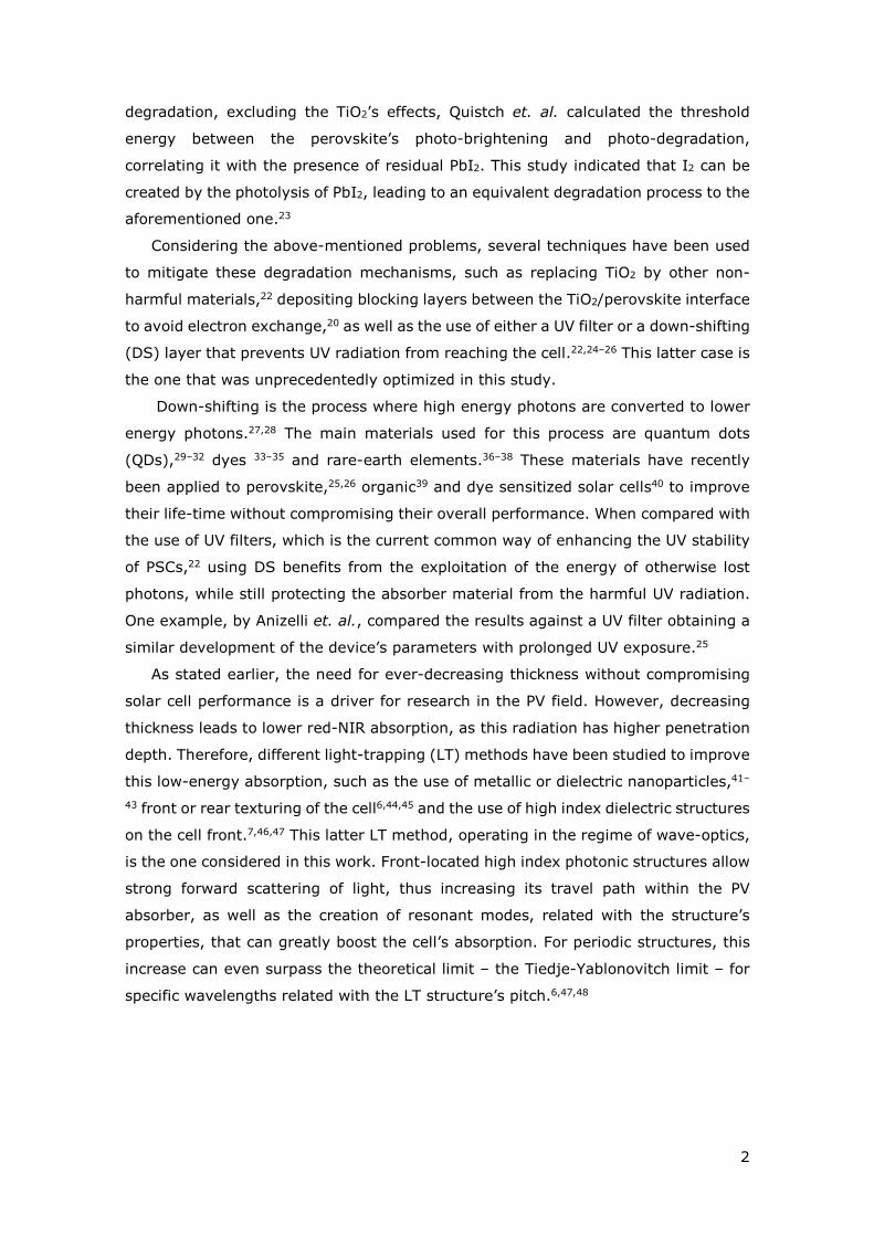
The bar chart of Figure 4 summarizes the key results from this work. Starting
with the photocurrent chart (Figure 4 a)), a first point to be made is the higher current
for the 500 nm PSCs, resulting from the thicker absorber. This difference is due to
higher red-NIR radiation absorption, as demonstrated in Figure 2 b) for the PC and
Figure 3 b) for the LTC. Secondly, the higher Jph for the PC with nBackground of 1.5,
when compared to the equivalent cell with index of 1, stems from better index
matching between the background and the front material in the cell (ITO), as seen
in Figure S3. On the other hand, it can also be seen that the LTCs have higher Jph
when compared with their planar counterpart. This increase clearly demonstrates the
benefits of using photonic structures for LT, allowing for optically thick but physically
thin devices.
The graph also indicates small current increases when using the optimized
spectrum. Considering that electrical losses are neglected in these studies, it can be
inferred from Figure 4 a) that these materials do not show a pronounced increase in
optical performance. However, these same effects, such as bulk instead of surface
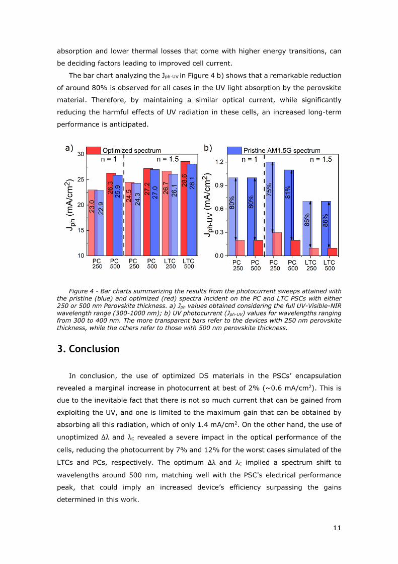
11
absorption and lower thermal losses that come with higher energy transitions, can
be deciding factors leading to improved cell current.
The bar chart analyzing the Jph-UV in Figure 4 b) shows that a remarkable reduction
of around 80% is observed for all cases in the UV light absorption by the perovskite
material. Therefore, by maintaining a similar optical current, while significantly
reducing the harmful effects of UV radiation in these cells, an increased long-term
performance is anticipated.
Figure 4 - Bar charts summarizing the results from the photocurrent sweeps attained with
the pristine (blue) and optimized (red) spectra incident on the PC and LTC PSCs with either
250 or 500 nm Perovskite thickness. a) Jph values obtained considering the full UV-Visible-NIR
wavelength range (300-1000 nm); b) UV photocurrent (Jph-UV) values for wavelengths ranging
from 300 to 400 nm. The more transparent bars refer to the devices with 250 nm perovskite
thickness, while the others refer to those with 500 nm perovskite thickness.
3. Conclusion
In conclusion, the use of optimized DS materials in the PSCs’ encapsulation
revealed a marginal increase in photocurrent at best of 2% (~0.6 mA/cm2). This is
due to the inevitable fact that there is not so much current that can be gained from
exploiting the UV, and one is limited to the maximum gain that can be obtained by
absorbing all this radiation, which of only 1.4 mA/cm2. On the other hand, the use of
unoptimized and revealed a severe impact in the optical performance of the
cells, reducing the photocurrent by 7% and 12% for the worst cases simulated of the
LTCs and PCs, respectively. The optimum and implied a spectrum shift to
wavelengths around 500 nm, matching well with the PSC's electrical performance
peak, that could imply an increased device’s efficiency surpassing the gains
determined in this work.

12
Importantly, from the analysis of the perovskite stability, one obtained a
significant reduction in the TiO2 harmful photo-generation of one order of magnitude,
coupled with an increase in the perovskite’s bulk generation. The LTCs revealed a
further decrease in the TiO2 photo-generation near the perovskite/TiO2 interface due
to the UV shading effect provided by the LT structures. By assessing the perovskite
UV photocurrent for the different simulated cells, reductions up to 86% were obtained
when comparing Jph values for the pristine and changed spectrum. Therefore, from
these analyses, one can infer that the use of LDS avoids the unwanted effects of UV
radiation on the perovskite, demonstrated by the hefty decrease in UV absorption
coupled with the diminished TiO2 photoactivity resulting from lower photo-
generation.
Acknowledgments
This work was funded by FEDER funds, through the COMPETE 2020 Program, and
national funds, through the Portuguese Foundation for Science and Technology (FCT-
MEC), under the projects POCI-01-0145-FEDER-007688 (Reference
UID/CTM/50025), ALTALUZ (Reference PTDC/CTM-ENE/5125/2014), SuperSolar
(PTDC/NAN-OPT/28430/2017) and TACIT (PTDC/NAN-OPT/28837/2017). The
authors also acknowledge funding from the European Project APOLO (H2020-LCE-
2017-RES-RIA, grant 763989). M. J. Mendes and S. Haque acknowledge funding by
FCT-MEC through the grants SFRH/BPD/115566/2016 and PD/BD/143031/2018 (via
AdvaMTech PhD program), respectively.
Supplementary Information
The details of the material’s properties used for the simulations, and additional
complementary figures are provided in supplementary information.
Author Contributions
M.A conceived and executed the simulation methodology, analyzed the results
and wrote the manuscript. M.C. assisted in developing the simulation methodology
and results analysis. S.H. assisted in the figures’ composition and provided the
parameters for the solar cells’ simulation. M.J.M. projected and supervised the
theoretical investigations presented here and assisted in the simulation methodology
and results analysis. H.A. assisted in supervising the work, discussed the results, and
revised the manuscript. E.F. and R.M. revised the manuscript and supervised the
work and financing projects.
13
References
(1) SolarPower Europe. Global Market Outlook for Solar Power 2017-2021.
Solarpower Europe 2017.
(2) Philipps, S.; Warmuth, W. ©Fraunhofer ISE: Photovoltaics Report. 2018, p 45.
(3) International Energy Agency. Snapshot of Global Photovoltaic Markets. 2017.
(4) Green, M. A. Commercial Progress and Challenges for Photovoltaics. Nat.
Energy 2016, 1 (1), 15015. https://doi.org/10.1038/nenergy.2015.15.
(5) Brongersma, M. L.; Cui, Y.; Fan, S. Light Management for Photovoltaics Using
High-Index Nanostructures. Nat. Mater. 2014, 13 (5), 451–460.
https://doi.org/10.1038/nmat3921.
(6) Isabella, O.; Vismara, R.; Linssen, D. N. P.; Wang, K. X.; Fan, S.; Zeman, M.
Advanced Light Trapping Scheme in Decoupled Front and Rear Textured Thin-
Film Silicon Solar Cells. Sol. Energy 2018, 162 (October 2017), 344–356.
https://doi.org/10.1016/j.solener.2018.01.040.
(7) Mendes, M. J.; Haque, S.; Sanchez-Sobrado, O.; Araújo, A.; Águas, H.;
Fortunato, E.; Martins, R. Optimal-Enhanced Solar Cell Ultra-Thinning with
Broadband Nanophotonic Light Capture. iScience 2018, 3, 238–254.
https://doi.org/10.1016/j.isci.2018.04.018.
(8) T. Vicente, A.; Araújo, A.; Mendes, M. J.; Nunes, D.; Oliveira, M. J.; Sanchez-
Sobrado, O.; Ferreira, M. P.; Águas, H.; Fortunato, E.; Martins, R.
Multifunctional Cellulose-Paper for Light Harvesting and Smart Sensing
Applications. J. Mater. Chem. C 2018, 6 (13), 3143–3181.
https://doi.org/10.1039/C7TC05271E.
(9) Correa-Baena, J.-P.; Saliba, M.; Buonassisi, T.; Grätzel, M.; Abate, A.; Tress,
W.; Hagfeldt, A. Promises and Challenges of Perovskite Solar Cells. Science
(80-. ). 2017, 358 (6364), 739–744.
https://doi.org/10.1126/science.aam6323.
(10) Filip, M. R.; Verdi, C.; Giustino, F. GW Band Structures and Carrier Effective
Masses of CH3NH3PbI3 and Hypothetical Perovskites of the Type APbI3 : A =
NH4, PH4, AsH4, and SbH4. J. Phys. Chem. C 2015, 119 (45), 25209–25219.
https://doi.org/10.1021/acs.jpcc.5b07891.
(11) Yin, W.-J.; Yang, J.-H.; Kang, J.; Yan, Y.; Wei, S.-H. Halide Perovskite
Materials for Solar Cells: A Theoretical Review. J. Mater. Chem. A 2015, 3
(17), 8926–8942. https://doi.org/10.1039/C4TA05033A.
(12) Brenner, T. M.; Egger, D. A.; Kronik, L.; Hodes, G.; Cahen, D. Hybrid Organic—
inorganic Perovskites: Low-Cost Semiconductors with Intriguing Charge-
Transport Properties. Nat. Rev. Mater. 2016, 1 (1), 15007.
https://doi.org/10.1038/natrevmats.2015.7.
14
(13) Jeon, N. J.; Noh, J. H.; Yang, W. S.; Kim, Y. C.; Ryu, S.; Seo, J.; Seok, S. Il.
Compositional Engineering of Perovskite Materials for High-Performance Solar
Cells. Nature 2015, 517 (7535), 476–480.
https://doi.org/10.1038/nature14133.
(14) Phillips, L. J.; Rashed, A. M.; Treharne, R. E.; Kay, J.; Yates, P.; Mitrovic, I.
Z.; Weerakkody, A.; Hall, S.; Durose, K. Dispersion Relation Data for
Methylammonium Lead Triiodide Perovskite Deposited on a (100) Silicon Wafer
Using a Two-Step Vapour-Phase Reaction Process. Data Br. 2015, 5, 926–928.
https://doi.org/10.1016/j.dib.2015.10.026.
(15) Kojima, A.; Teshima, K.; Shirai, Y.; Miyasaka, T. Organometal Halide
Perovskites as Visible-Light Sensitizers for Photovoltaic Cells. J. Am. Chem.
Soc. 2009, 131 (17), 6050–6051. https://doi.org/10.1021/ja809598r.
(16) Fu, F.; Feurer, T.; Weiss, T. P.; Pisoni, S.; Avancini, E.; Andres, C.; Buecheler,
S.; Tiwari, A. N. High-Efficiency Inverted Semi-Transparent Planar Perovskite
Solar Cells in Substrate Configuration. Nat. Energy 2017, 2 (1), 16190.
https://doi.org/10.1038/nenergy.2016.190.
(17) Yang, W. S.; Noh, J. H.; Jeon, N. J.; Kim, Y. C.; Ryu, S.; Seo, J.; Seok, S. I.
High-Performance Photovoltaic Perovskite Layers Fabricated through
Intramolecular Exchange. Science (80-. ). 2015, 348 (6240), 1234–1237.
https://doi.org/10.1126/science.aaa9272.
(18) Asghar, M. I.; Zhang, J.; Wang, H.; Lund, P. D. Device Stability of Perovskite
Solar Cells – A Review. Renew. Sustain. Energy Rev. 2017, 77 (July 2016),
131–146. https://doi.org/10.1016/j.rser.2017.04.003.
(19) Lee, S.-W.; Kim, S.; Bae, S.; Cho, K.; Chung, T.; Mundt, L. E.; Lee, S.; Park,
S.; Park, H.; Schubert, M. C.; et al. UV Degradation and Recovery of Perovskite
Solar Cells. Sci. Rep. 2016, 6 (1), 38150. https://doi.org/10.1038/srep38150.
(20) Ito, S.; Tanaka, S.; Manabe, K.; Nishino, H. Effects of Surface Blocking Layer
of Sb 2 S 3 on Nanocrystalline TiO2 for CH3NH3PbI3 Perovskite Solar Cells. J.
Phys. Chem. C 2014, 118 (30), 16995–17000.
https://doi.org/10.1021/jp500449z.
(21) Farooq, A.; Hossain, I. M.; Moghadamzadeh, S.; Schwenzer, J. A.; Abzieher,
T.; Richards, B. S.; Klampaftis, E.; Paetzold, U. W. Spectral Dependence of
Degradation under Ultraviolet Light in Perovskite Solar Cells. ACS Appl. Mater.
Interfaces 2018, 10 (26), 21985–21990.
https://doi.org/10.1021/acsami.8b03024.
(22) Leijtens, T.; Eperon, G. E.; Pathak, S.; Abate, A.; Lee, M. M.; Snaith, H. J.
Overcoming Ultraviolet Light Instability of Sensitized TiO2 with Meso-
Superstructured Organometal Tri-Halide Perovskite Solar Cells. Nat. Commun.
15
2013, 4, 1–8. https://doi.org/10.1038/ncomms3885.
(23) Quitsch, W.-A.; DeQuilettes, D. W.; Pfingsten, O.; Schmitz, A.; Ognjanovic,
S.; Jariwala, S.; Koch, S.; Winterer, M.; Ginger, D. S.; Bacher, G. The Role of
Excitation Energy in Photobrightening and Photodegradation of Halide
Perovskite Thin Films. J. Phys. Chem. Lett. 2018, 9 (8), 2062–2069.
https://doi.org/10.1021/acs.jpclett.8b00212.
(24) Gheno, A.; Trigaud, T.; Bouclé, J.; Audebert, P.; Ratier, B.; Vedraine, S.
Stability Assessments on Luminescent Down-Shifting Molecules for UV-
Protection of Perovskite Solar Cells. Opt. Mater. (Amst). 2018, 75, 781–786.
https://doi.org/10.1016/j.optmat.2017.11.027.
(25) Anizelli, H. S.; Stoichkov, V.; Fernandes, R. V.; Duarte, J. L.; Laureto, E.;
Kettle, J.; Visoly-Fisher, I.; Katz, E. A. Application of Luminescence
Downshifting Materials for Enhanced Stability of CH3NH3PbI3(1-x)Cl3x Perovskite
Photovoltaic Devices. Org. Electron. 2017, 49, 129–134.
https://doi.org/10.1016/j.orgel.2017.06.056.
(26) Chander, N.; Khan, A. F.; Chandrasekhar, P. S.; Thouti, E.; Swami, S. K.;
Dutta, V.; Komarala, V. K. Reduced Ultraviolet Light Induced Degradation and
Enhanced Light Harvesting Using YVO4:Eu3+ down-Shifting Nano-Phosphor
Layer in Organometal Halide Perovskite Solar Cells. Appl. Phys. Lett. 2014,
105 (3), 033904. https://doi.org/10.1063/1.4891181.
(27) Klampaftis, E.; Ross, D.; McIntosh, K. R.; Richards, B. S. Enhancing the
Performance of Solar Cells via Luminescent Down-Shifting of the Incident
Spectrum: A Review. Sol. Energy Mater. Sol. Cells 2009, 93 (8), 1182–1194.
https://doi.org/10.1016/j.solmat.2009.02.020.
(28) Liu, N.; Xue, H.; Ji, Y.; Wang, J. ZnSe/ZnS Core-Shell Quantum Dots
Incorporated with Ag Nanoparticles as Luminescent down-Shifting Layers to
Enhance the Efficiency of Si Solar Cells. J. Alloys Compd. 2018, 747, 696–702.
https://doi.org/10.1016/j.jallcom.2018.03.060.
(29) Lesyuk, R.; Lesnyak, V.; Herguth, A.; Popovych, D.; Bobitski, Y.; Klinke, C.;
Gaponik, N. Simulation Study of Environmentally Friendly Quantum-Dot-Based
Photovoltaic Windows. J. Mater. Chem. C 2017, 5 (45), 11790–11797.
https://doi.org/10.1039/C7TC02945D.
(30) Lesyuk, R.; Marinov, V.; Hobbie, E. K.; Elbaradei, A.; Tarnavchyk, I.; Bobitski,
Y. Toward Cadmium-Free Spectral down-Shifting Converters for Photovoltaic
Applications. Sol. Energy Mater. Sol. Cells 2016, 151, 52–59.
https://doi.org/10.1016/j.solmat.2016.02.021.
(31) Chatten, A. J.; Barnham, K. W. J.; Buxton, B. F.; Ekins-Daukes, N. J.; Malik,
M. A. A New Approach to Modelling Quantum Dot Concentrators. Sol. Energy
16
Mater. Sol. Cells 2003, 75 (3–4), 363–371. https://doi.org/10.1016/S0927-
0248(02)00182-4.
(32) Chatten, A. J.; Barnham, K. W. J.; Buxton, B. F.; Ekins-Daukes, N. J.; Malik,
M. A. Quantum Dot Solar Concentrators. Semiconductors 2004, 38 (8), 909–
917. https://doi.org/10.1134/1.1787111.
(33) Rondão, R.; Frias, A. R.; Correia, S. F. H.; Fu, L.; de Zea Bermudez, V.; André,
P. S.; Ferreira, R. A. S.; Carlos, L. D. High-Performance Near-Infrared
Luminescent Solar Concentrators. ACS Appl. Mater. Interfaces 2017, 9 (14),
12540–12546. https://doi.org/10.1021/acsami.7b02700.
(34) Lipovšek, B.; Solodovnyk, A.; Forberich, K.; Stern, E.; Krč, J.; Brabec, C. J.;
Topič, M. Optical Model for Simulation and Optimization of Luminescent Down-
Shifting Layers Filled with Phosphor Particles for Photovoltaics. Opt. Express
2015, 23 (15), A882. https://doi.org/10.1364/OE.23.00A882.
(35) McIntosh, K. R.; Lau, G.; Cotsell, J. N.; Hanton, K.; Bätzner, D. L.; Bettiol, F.;
Richards, B. S. Increase in External Quantum Efficiency of Encapsulated Silicon
Solar Cells from a Luminescent Down-Shifting Layer. Prog. Photovoltaics Res.
Appl. 2009, 17 (3), 191–197. https://doi.org/10.1002/pip.867.
(36) Correia, S. F. H.; Lima, P. P.; Pecorato, E.; Ribeiro, S. J. L.; André, P. S.;
Ferreira, R. A. S.; Carlos, L. D. Scale up the Collection Rea of Luminescent
Solar Concentrators towards Metre-Length Flexible Waveguiding Photovoltaics.
Prog. Photovoltaics Res. Appl. 2016, 24, 1178–1193.
https://doi.org/10.1002/pip.
(37) Correia, S. F. H.; Lima, P. P.; André, P. S.; Ferreira, M. R. S.; Carlos, L. A. D.
High-Efficiency Luminescent Solar Concentrators for Flexible Waveguiding
Photovoltaics. Sol. Energy Mater. Sol. Cells 2015, 138, 51–57.
https://doi.org/10.1016/j.solmat.2015.02.032.
(38) Wiegman, J. W. E.; van der Kolk, E. Building Integrated Thin Film Luminescent
Solar Concentrators: Detailed Efficiency Characterization and Light Transport
Modelling. Sol. Energy Mater. Sol. Cells 2012, 103, 41–47.
https://doi.org/10.1016/j.solmat.2012.04.016.
(39) Kettle, J.; Bristow, N.; Gethin, D. T.; Tehrani, Z.; Moudam, O.; Li, B.; Katz, E.
A.; dos Reis Benatto, G. A.; Krebs, F. C. Printable Luminescent down Shifter
for Enhancing Efficiency and Stability of Organic Photovoltaics. Sol. Energy
Mater. Sol. Cells 2016, 144, 481–487.
https://doi.org/10.1016/j.solmat.2015.09.037.
(40) Llanos, J.; Brito, I.; Espinoza, D.; Sekar, R.; Manidurai, P. A Down-Shifting
Eu3+-Doped Y2WO6/TiO2 Photoelectrode for Improved Light Harvesting in Dye-
Sensitized Solar Cells. R. Soc. Open Sci. 2018, 5 (2), 171054.
17
https://doi.org/10.1098/rsos.171054.
(41) Yin, G.; Manley, P.; Schmid, M. Light Trapping in Ultrathin CuIn1-xGaxSe2 Solar
Cells by Dielectric Nanoparticles. Sol. Energy 2018, 163 (January), 443–452.
https://doi.org/10.1016/j.solener.2018.01.096.
(42) Baranov, D. G.; Zuev, D. A.; Lepeshov, S. I.; Kotov, O. V.; Krasnok, A. E.;
Evlyukhin, A. B.; Chichkov, B. N. All-Dielectric Nanophotonics: The Quest for
Better Materials and Fabrication Techniques. 2017, 4 (7).
https://doi.org/10.1364/OPTICA.4.000814.
(43) Bhattacharya, J.; Chakravarty, N.; Pattnaik, S.; Dennis Slafer, W.; Biswas, R.;
Dalal, V. L. A Photonic-Plasmonic Structure for Enhancing Light Absorption in
Thin Film Solar Cells. Appl. Phys. Lett. 2011, 99 (13), 131114.
https://doi.org/10.1063/1.3641469.
(44) Xiao, J.; Fang, H.; Su, R.; Li, K.; Song, J.; Krauss, T. F.; Li, J.; Martins, E. R.
Paths to Light Trapping in Thin Film GaAs Solar Cells. Opt. Express 2018, 26
(6), A341. https://doi.org/10.1364/OE.26.00A341.
(45) Donie, Y. J.; Smeets, M.; Egel, A.; Lentz, F.; Preinfalk, J. B.; Mertens, A.;
Smirnov, V.; Lemmer, U.; Bittkau, K.; Gomard, G. Light Trapping in Thin Film
Silicon Solar Cells via Phase Separated Disordered Nanopillars. Nanoscale
2018, 10 (14), 6651–6659. https://doi.org/10.1039/C8NR00455B.
(46) Sanchez-Sobrado, O.; Mendes, M. J.; Haque, S.; Mateus, T.; Araujo, A.;
Aguas, H.; Fortunato, E.; Martins, R. Colloidal-Lithographed TiO2 Photonic
Nanostructures for Solar Cell Light Trapping. J. Mater. Chem. C 2017, 5 (27),
6852–6861. https://doi.org/10.1039/C7TC01756A.
(47) Grandidier, J.; Deceglie, M. G.; Callahan, D. M.; Atwater, H. A. Simulations of
Solar Cell Absorption Enhancement Using Resonant Modes of a Nanosphere
Array. In Physics, Simulation, and Photonic Engineering of Photovoltaic
Devides; Freundlich, A., Guillemoles, J.-F. F., Eds.; 2012; Vol. 8256, p 825603.
https://doi.org/10.1117/12.909677.
(48) Deceglie, M. G.; Ferry, V. E.; Alivisatos, A. P.; Atwater, H. A. Design of
Nanostructured Solar Cells Using Coupled Optical and Electrical Modeling. Nano
Lett. 2012, 12 (6), 2894–2900. https://doi.org/10.1021/nl300483y.
(49) Haque, S.; Mendes, M. J. de M. D.; Sanchez-Sobrado, O.; Águas, H.;
Fortunato, E.; Martins, R. Photonic-Structured TiO2 for High-Efficiency, Flexible
and Stable Perovskite Solar Cells. Nano Energy 2019, 59 (January), 91–101.
https://doi.org/10.1016/j.nanoen.2019.02.023.
(50) Uekert, T.; Solodovnyk, A.; Ponomarenko, S.; Osvet, A.; Levchuk, I.; Gast, J.;
Batentschuk, M.; Forberich, K.; Stern, E.; Egelhaaf, H.-J.; et al.
Nanostructured Organosilicon Luminophores in Highly Efficient Luminescent
18
Down-Shifting Layers for Thin Film Photovoltaics. Sol. Energy Mater. Sol. Cells
2016, 155, 1–8. https://doi.org/10.1016/j.solmat.2016.04.019.
(51) Lumerical Inc. https://www.lumerical.com/, Last accessed on: March 2019.
(52) Purcell-Milton, F.; Gun’ko, Y. K. Quantum Dots for Luminescent Solar
Concentrators. J. Mater. Chem. 2012, 22 (33), 16687.
https://doi.org/10.1039/c2jm32366d.
(53) Wang, B.; Li, B.; Shen, T.; Li, M.; Tian, J. ZnSe Quantum Dots Downshifting
Layer for Perovskite Solar Cells. J. Energy Chem. 2018, 27 (3), 736–741.
https://doi.org/10.1016/j.jechem.2017.11.021.
(54) Richards, B. S.; McIntosh, K. R. Overcoming the Poor Short Wavelength
Spectral Response of CdS/CdTe Photovoltaic Modules via Luminescence down-
Shifting: Ray-Tracing Simulations. Prog. Photovoltaics Res. Appl. 2007, 15
(1), 27–34. https://doi.org/10.1002/pip.723.
(55) National Energy Renewable Laboratory (NREL) https://www.nrel.gov/, Last
accessed on: March 2019.
(56) Hou, X.; Xuan, T.; Sun, H.; Chen, X.; Li, H.; Pan, L. High-Performance
Perovskite Solar Cells by Incorporating a ZnGa2O4:Eu3+ Nanophosphor in the
Mesoporous TiO2 Layer. Sol. Energy Mater. Sol. Cells 2016, 149, 121–127.
https://doi.org/10.1016/j.solmat.2016.01.021.
(57) Yang, Y.; Yang, M.; Moore, D. T.; Yan, Y.; Miller, E. M.; Zhu, K.; Beard, M. C.
Top and Bottom Surfaces Limit Carrier Lifetime in Lead Iodide Perovskite Films.
Nat. Energy 2017, 2 (2), 16207. https://doi.org/10.1038/nenergy.2016.207.
Recommended