Embed Size (px)
Citation preview

Miguel Diogo Furtado Alexandre
Licenciado em Engenharia de Micro e Nanotecnologias
Theoretical Study of Optimum LuminescentDown-Shifting Properties for High Efficiency
and Stable Perovskite Solar Cells
Dissertação para obtenção do Grau de Mestre em
Engenharia de Micro e Nanotecnologias
Orientador: Manuel J. Mendes, Post-Doc Fellow and Invited Assis-tant Professor,Faculty of Sciences and Technology, NOVA Universityof Lisbon
Co-orientador: Rodrigo Martins, Full Professor,Faculty of Sciences and Technology, NOVA Universityof Lisbon
Júri
Presidente: Dr. Hugo Manuel Brito ÁguasArguente: Dr. Maria Rute de Amorim e Sá Ferreira André
Vogal: Dr. Manuel João de Moura Dias Mendes
November, 2018


Theoretical Study of Optimum Luminescent Down-Shifting Properties for HighEfficiency and Stable Perovskite Solar Cells
Copyright © Miguel Diogo Furtado Alexandre, Faculdade de Ciências e Tecnologia, Uni-
versidade NOVA de Lisboa.
A Faculdade de Ciências e Tecnologia e a Universidade NOVA de Lisboa têm o direito,
perpétuo e sem limites geográficos, de arquivar e publicar esta dissertação através de
exemplares impressos reproduzidos em papel ou de forma digital, ou por qualquer outro
meio conhecido ou que venha a ser inventado, e de a divulgar através de repositórios
científicos e de admitir a sua cópia e distribuição com objetivos educacionais ou de inves-
tigação, não comerciais, desde que seja dado crédito ao autor e editor.
Este documento foi gerado utilizando o processador (pdf)LATEX, com base no template “novathesis” [1] desenvolvido no Dep. Informática da FCT-NOVA [2].[1] https://github.com/joaomlourenco/novathesis [2] http://www.di.fct.unl.pt


I would like to dedicate this work to my family.


Acknowledgements
Em primeiro lugar, gostaria de agradecer ao Professor Rodrigo Martins e à Professora
Elvira Fortunato, por terem sido os fundadores deste magnífico curso onde estive nos
últimos 5 anos, que me levou à descoberta de novas áreas, culminando no trabalho que
aqui apresento.
Gostaria também de agradecer ao meu orientador, Professor Manuel Mendes, e co-
orientador, Professor Rodrigo Martins, pela oportunidade de fazer uma tese na área dos
fotovoltaicos, que é um tema de significante interesse para mim. Aos nomes anteriores,
gostaria também de adicionar o Professor Hugo Águas e o Mestre Sirazul Zakir, pela ajuda
e orientação que me deram durante este processo.
Não posso também deixar de fora todos os professores que, ao longo de todos os meus
anos de ensino, me ajudaram a adquirir o conhecimento que hoje possuo, sendo que este
trabalho não teria sido possível sem as suas contribuições.
Um obrigado muito especial para a minha família que sempre me suportou em todos
os desafios que tive ao longo dos anos. Em especial, gostaria de mencionar o meu pai,
a minha mãe e a minha irmã, que sempre foram as primeiras pessoas a ajudar-me a
ultrapassar os problemas que tive, assim como, pelo seu esforço, também me permitiram
que tivesse tido estes últimos 5 anos que significaram muito para mim.
Gostaria também de agradecer aos meus colegas Fábio Vieira e Manuel Chapa, com
quem tive uma excelente semana para escrutinar teses, que ajudou a colmatar muitas das
lacunas e bengalas que temos na escrita.
Por fim, mas não menos importante, gostaria também de agradecer aos meus amigos,
com quem passei excelentes momentos ao longo destes últimos anos. Em especial, destaco
os nomes João Teles, Manuel Chapa, Fábio Vieira, Débora Magalhães, João Pina, Ricardo
Viana e Catarina Marques, Ana Pinheiro, Rita Fragoso e Maria Helena, sendo estas as
pessoas com quem me dei mais.
vii


Abstract
In recent years, the discovery of the excellent optical and electrical properties of per-
ovskite materials made them one of focus of research in the area of photovoltaics, with
its efficiency increasing significantly since its inception, in 2009. However, problems
associated with the stability of these materials have hindered their widescale market ap-
plication, with two examples being the UV degradation of the absorber material and the
photoactivity, under 400 nm wavelengths, of TiO2 which is one of the main materials
used as an electron transport layer in these cells. Consequently, different methods were
studied to minimize this degradation. One example consists in using down-shifting ma-
terials that change the harmful UV radiation to higher wavelengths that have no effect on
the cell stability. Thus, this work is focused in the theoretical study of the photocurrent
gains that can be attained by emulating the changed spectrum resulting from applying
these materials, as well as the reduction in the harmful effects of UV radiation on per-
ovskite solar cells. This first case analyzed resulted in gains of around 1% for planar cells
and around 2% for cells with photonic structures. For the second optimized case, one
was able to obtain a general reduction in generation in TiO2 of one order of magnitude,
coupled with a 80% reduction of perovskite’s UV absorption.
Keywords: Photovoltaics, Photonic-enhanced Perovskite Solar Cells, Ultraviolet Stability,
Down-shifting, Light Trapping
ix


Resumo
A recente descoberta das excelentes propriedades óticas e elétricas das perovskites, para
aplicações em células solares, fez com que se tornassem num dos principais alvos de
estudo na área dos fotovoltaicos, levando ao rápido aumento da sua eficiência desde que
foram introduzidas. Contudo, problemas associados com a estabilidade destes materiais
tem limitado a sua implementação à larga escala. Alguns exemplos são a degradação do
material fotoativo quando exposto a radiação UV, assim como a fotoatividade do TiO2,
para comprimentos de onda inferiores a 400 nm, uma vez que este se trata de um dos
materiais mais usados como camada de transporte de eletrões nestas células. Consequen-
temente, diferentes métodos estão a ser estudados, de forma a minimizar esta degradação.
Um exemplo, consiste em fazer down-shifting da radiação solar de forma a mudar a nefasta
radiação UV para comprimentos de onda que não impactem a perovskite negativamente.
Desta forma, este trabalho foca-se no estudo teórico dos ganhos de corrente gerada na
célula devido à aplicação de down-shifting, em conjunto com os efeitos na nefasta geração
no TiO2. No primeiro caso, ganhos de cerca de 1% foram obtidos para células planares e
cerca de 2% para células com estruturas fotónicas. Para o segundo caso otimizado obteve-
se uma redução de uma ordem de grandeza na geração no TiO2 e uma redução de 80%
para a radiação UV absorvida pela perovskite.
Palavras-chave: Fotovoltaicos, Células Solares de Perovskite com Estruturas Fotónicas,
Estabilidade à Radiação Ultravioleta, Down-shifting, Aprisionamento de Luz
xi


Contents
List of Figures xv
List of Tables xix
Symbols xxi
Acronyms xxiii
Motivation and Objectives xxv
Work Strategy xxvii
1 Introduction 1
1.1 Solar Cell Market . . . . . . . . . . . . . . . . . . . . . . . . . . . . . . . . 1
1.2 Perovskite Solar Cells . . . . . . . . . . . . . . . . . . . . . . . . . . . . . . 1
1.3 Luminescent Down-Shifting . . . . . . . . . . . . . . . . . . . . . . . . . . 3
1.4 Dielectric Photonic Structures . . . . . . . . . . . . . . . . . . . . . . . . . 4
1.5 Finite-Difference Time-Domain Simulation . . . . . . . . . . . . . . . . . 4
2 Simulation Setup 7
2.1 Solar Cell Structure . . . . . . . . . . . . . . . . . . . . . . . . . . . . . . . 7
3 Results and Discussion 9
3.1 Optical simulation . . . . . . . . . . . . . . . . . . . . . . . . . . . . . . . . 9
3.2 Down Shifted Spectrum . . . . . . . . . . . . . . . . . . . . . . . . . . . . 10
3.3 Planar Perovskite Solar Cells . . . . . . . . . . . . . . . . . . . . . . . . . . 10
3.3.1 Reflection Profiles . . . . . . . . . . . . . . . . . . . . . . . . . . . . 11
3.3.2 Absorption Profiles . . . . . . . . . . . . . . . . . . . . . . . . . . . 13
3.3.3 Photocurrent Shifts . . . . . . . . . . . . . . . . . . . . . . . . . . . 15
3.3.4 Generation Profiles and UV absorption . . . . . . . . . . . . . . . . 18
3.4 Solar Cells with Dielectric Photonic Structures . . . . . . . . . . . . . . . 20
3.4.1 Reflection Profiles . . . . . . . . . . . . . . . . . . . . . . . . . . . . 22
3.4.2 Absorption Profiles . . . . . . . . . . . . . . . . . . . . . . . . . . . 22
3.4.3 Photocurrent Shifts . . . . . . . . . . . . . . . . . . . . . . . . . . . 23
xiii

CONTENTS
3.4.4 Generation Profiles . . . . . . . . . . . . . . . . . . . . . . . . . . . 26
3.5 Final Thoughts . . . . . . . . . . . . . . . . . . . . . . . . . . . . . . . . . . 27
4 Conclusion and Future Perspectives 29
References 31
I Equations for the FDTD method 39
II Simulation Parameters 41
III Simulated Transmissions 43
xiv

List of Figures
1.1 Unit cell for the basic ABX3 perovskite structure. The circle sizes represent
the different ion radius, meaning the A ion is the largest and the X ion the
smallest. The colors refer to the different ions used. MA, EA and FA stand for
methylammonium, ethylammonium and formamidinium, respectively. . . . 2
1.2 Schematic of the main PSCs architectures. a) cell with n-i-p configuration
and mesoporous layer, b) cell with n-i-p configuration and c) cell with p-i-n
configuration. . . . . . . . . . . . . . . . . . . . . . . . . . . . . . . . . . . . . 3
1.3 Schematic representation of the Yee algorithm. On the left is shown the Yee
cell with the various corresponding fields. The direction of the fields in each
face is chosen to satisfy Faraday’s law. On the right, is shown the field with the
full notation, including the spatial coordinates for the top face of the cube. . 5
2.1 Schematic of the solar cells used in the simulations. a) Cell with planar struc-
ture, PC, used as reference and b) Cell with light trapping structures, LTC.
The dimensions of the cell on the right refer to their respective counterparts
in Table 2.1. The different layers properties are shown in Annex II. . . . . . . 8
3.1 a) In solid line are the absorbed and emitted fluxes for λC of 350 nm and ∆λ of
200 nm. In dash line is the gaussian profile used to calculate the absorbed and
emitted fluxes; b) Modelled spectra transmitted through a window prototype
with varying QD properties and quantum yield of 50%. Adapted from refer-
ence [40]; c) Schematic of the DS process, where higher wavelength radiation
is redshifted. . . . . . . . . . . . . . . . . . . . . . . . . . . . . . . . . . . . . . 11
3.2 Resulting irradiance plots of the DS process used to simulate the effect of a LDS
layer. a) AM1.5G spectrum, in black, and 2 examples of resulting spectrums
when the ∆λ remains constant as 310 nm and λC changes from 300 nm to
400 nm, in red and blue, respectively, b) AM1.5G spectrum, in black, and 2
examples of the resulting spectrums when λC remains constant at 300 nm and
∆λ varies from 205 nm to 400 nm, in red and blue, respectively. . . . . . . . 12
xv

List of Figures
3.3 Reflection profiles with the results from the numerical simulation, in black,
and the results from the theoretical simulation, in red. Inset is represented
the modulus of the difference between the two methods. a) PC with 250 nm
perovskite, b) PC with 500 nm perovskite, c) PC with background index of
1.5 and 250 nm perovskite, d) PC with background index of 1.5 and 500 nm
perovskite. . . . . . . . . . . . . . . . . . . . . . . . . . . . . . . . . . . . . . . 13
3.4 Absorption profiles with the absorption on the perovskite layer, in black; the
TiO2 layer, in red; and the total cell absorption, in green. The inset profiles
show the plots for the absorbed power density through the cell volume for spe-
cific wavelengths, indicated by the arrows. The leftmost graph is the absorbed
power for 350 nm and the rightmost graph is the absorbed power for 900 nm.
a) and b) PC with VBI for 250 nm and 500 nm perovskite, respectively; c) and
d) PC with PBI for 250 nm and 500 nm perovskite, respectively. . . . . . . . 15
3.5 Contour plots for the sweeps where λC and ∆λ were varied from 300 nm to
400 nm and 100 nm to 400 nm, respectively. a) PC with VBI for 500 nm per-
ovskite layer and b) PC with VBI for 250 nm perovskite layer. The thicker line
represents the contour corresponding to the photocurrent value obtained for
the pristine spectrum. The indicated values represent the respective contour
photocurrent value. The topmost value refers to the contour representing the
pristine value, while the bottommost refers to the highest value contour in the
plot. . . . . . . . . . . . . . . . . . . . . . . . . . . . . . . . . . . . . . . . . . . 16
3.6 Contour plots for the sweeps where λC and ∆λwere varied from 300 nm to 400
nm and 100 nm to 400 nm, respectively. a) PC with PBI for 500 nm perovskite
layer, b) PC with PBI for 250 nm perovskite. The thicker line represents the
contour corresponding to the photocurrent value obtained for the pristine
spectrum. The indicated values represent the respective contour photocurrent
value. The topmost value refers to the contour representing the pristine value,
while the bottommost refers to the highest value contour in the plot. . . . . . 17
3.7 Generation profiles for the PCs with VBI. a) cell with 250 nm perovskite; b)
cell with 250 nm perovskite and optimized spectrum; c) cell with 500 nm
perovskite; d) cell with 500 nm perovskite and optimized spectrum. The
arrows and ellipse mark the biggest changes in the plots. . . . . . . . . . . . . 20
3.8 Generation profiles for the PCs with PBI. a) cell with 250 nm perovskite; b)
cell with 250 nm perovskite and optimized spectrum; c) cell with 500 nm
perovskite; d) cell with 500 nm perovskite and optimized spectrum. The
arrows and ellipse mark the biggest changes in the plots. . . . . . . . . . . . . 21
3.9 a) Reflection profile for the LTC, in black; and for the PC, in red; where both
have a 250 nm layer of perovskite absorber material. b) Reflection profile for
the LTC, in black; and for the PC, in red; where both have a 500 nm perovskite
absorber material. . . . . . . . . . . . . . . . . . . . . . . . . . . . . . . . . . . 22
xvi

List of Figures
3.10 a) Absorption profile for the LTC with 250 nm perovskite layer, b) absorption
profiles for the LTC with 500 nm perovskite layer. The shaded areas represent
the absorption of the TiO2, in red; and the remaining materials absorption, in
green. The black curve is the perovskite absorption. The inset plots represent
the absorbed power density for each respective cell for a wavelength of 350
nm, bottom graph, and 900 nm, top graph. . . . . . . . . . . . . . . . . . . . . 24
3.11 Contour plots for the sweeps where λC and ∆λ were changed from 300 nm
to 400 nm and 100 nm to 400 nm, respectively. a) Plot for the cell with 250
nm perovskite layer and b) plot for the cell with 500 nm perovskite layer. The
thicker line represents the contour corresponding to the photocurrent value
obtained for the pristine spectrum. The indicated values represent the re-
spective contour photocurrent value. The topmost value refers to the contour
representing the pristine value, while the bottommost refers to the highest
value contour in the plot. . . . . . . . . . . . . . . . . . . . . . . . . . . . . . . 25
3.12 Generation profiles for the LTC. a) cell with 250 nm perovskite; b) cell with
250 nm perovskite and optimized spectrum; c) cell with 500 nm perovskite;
d) cell with 500 nm perovskite and optimized spectrum. The arrows point to
the biggest plot changes. . . . . . . . . . . . . . . . . . . . . . . . . . . . . . . 27
3.13 a) Bar chart summarizing the pristine (red) and optimized (blue) Jph values
obtained from the photocurrent sweeps; b) Bar chart summarizing the Jph for
wavelengths ranging from 300 nm to 400 nm for the for the pristine (red) and
optimized spectrum (blue). . . . . . . . . . . . . . . . . . . . . . . . . . . . . . 28
II.1 Refractive index, n, and extinction coeficient, k, for the different material used
in the simulations. These values are provided by reference [80]. . . . . . . . . 41
III.1 Simulated and theoretical transmission for the planar cells. a) 250 nm per-
ovskite and b) 500 nm perovskite. . . . . . . . . . . . . . . . . . . . . . . . . . 43
III.2 Simulated and theoretical transmission for the planar cells with a background
index of 1.5. a) 250 nm perovskite and b) 500 nm perovskite. . . . . . . . . . 44
III.3 Simulated transmission for the cells with photonic structures and a back-
ground index of 1.5. a) 500 nm perovskite and b) 250 nm perovskite. . . . . 44
xvii


List of Tables
2.1 PC and LTC parameters. Ag, Spiro and ITO represent the respective material
thicknesses. TiO2, for the PC, represents the TiO2 thickness and for the LTC
is the TiO2 thickness between perovskite and the structures beginning. tV oidsis the structures’ TiO2 thickness. R is the voids x and y radius, while Rz is
the z radius. tV oids is the distance between the center of 2 consecutive void
structures, being given in function of R. . . . . . . . . . . . . . . . . . . . . . 8
3.1 Summary of the optimized results obtained for the different PCs simulated.
AM1.5G Jph represents the values obtained in the pristine case and Shifted Jphrepresents the optimized values resulting from the sweeps for each individual
case. It is also shown the absolute and relative difference between the two. . 19
3.2 ∆λ and λC values corresponding to the optimized values of Jph obtained from
the sweeps. . . . . . . . . . . . . . . . . . . . . . . . . . . . . . . . . . . . . . . 19
3.3 Optimized Jph results of the λC and ∆λ sweep done. It’s shown the pristine
results, AM1.5G Jph; the results corresponding to the maximum value obtained
from the sweep, Jph; and the absolute and relative difference between both
values ∆Jph. . . . . . . . . . . . . . . . . . . . . . . . . . . . . . . . . . . . . . . 24
3.4 ∆λ and λC , values corresponding to the optimum Jph values. The values on
the left represent the thickness of the perovskite used in the cell simulation. 26
II.1 Most important simulation parameters used, namely the different boundary
conditions for the various cells, the PML layers and the background mesh
used. The PC with PBI and VBI had the same simulation parameters. . . . . 42
xix

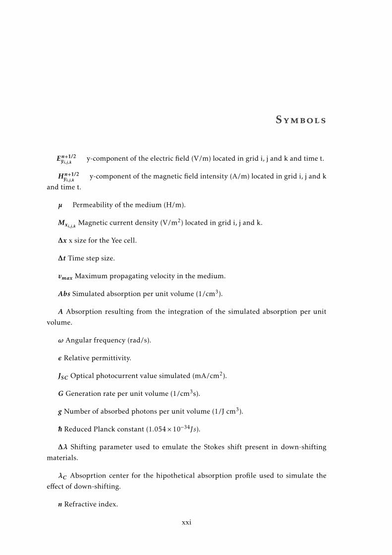
Symbols
En+1/2yi,j,k y-component of the electric field (V/m) located in grid i, j and k and time t.
Hn+1/2yi,j,k y-component of the magnetic field intensity (A/m) located in grid i, j and k
and time t.
µ Permeability of the medium (H/m).
Mxi,j,k Magnetic current density (V/m2) located in grid i, j and k.
∆x x size for the Yee cell.
∆t Time step size.
vmax Maximum propagating velocity in the medium.
Abs Simulated absorption per unit volume (1/cm3).
A Absorption resulting from the integration of the simulated absorption per unit
volume.
ω Angular frequency (rad/s).
ε Relative permittivity.
JSC Optical photocurrent value simulated (mA/cm2).
G Generation rate per unit volume (1/cm3s).
g Number of absorbed photons per unit volume (1/J cm3).
~ Reduced Planck constant (1.054× 10⁻³⁴Js).
∆λ Shifting parameter used to emulate the Stokes shift present in down-shifting
materials.
λC Absoprtion center for the hipothetical absorption profile used to simulate the
effect of down-shifting.
n Refractive index.
xxi

SYMBOLS
Rs Specular reflection.
Rd Difuse reflection.
xxii

Acronyms
a-Si Amorphous silicon.
CIGS CuInxGa1−xSe2.
c-Si Crystalline silicon.
DS Down-shifted.
EA CH3CH2NH+3 .
ETL Electron transport layer.
FA NH2CH=NH+2 .
FDTD Finite-difference time-domain.
HOIP Hybrid organic inorganic perovskite.
HTL Hole transport layer.
ITO Indium tin oxide.
LDS Luminescent down-shifting.
LSC Luminescent solar concentrators.
LTC Light trapping cell.
MA CH3NH+3 .
mp-TiO2 Mesoporous TiO2.
PBI Polymer background index.
PC Planar cell.
poly-Si Polycrystalline silicon.
PSC Perovskite solar cell.
PV Photovoltaic.
xxiii

ACRONYMS
QD Quantum dots.
RE Rare earths.
Spiro 2,2’,7,7’-tetrakis(N,N’-di-p-methoxyphenyl-amine)9,9’-spirobifluorene.
TCO Transparent conductive oxide.
UV Ultraviolet.
VBI Vacuum background index.
xxiv

Motivation and Objectives
The ever-growing demand for clean energy has been one of the main proponents of
research in the area of photovoltaics, with special focus on increasing the solar cells W/$
ratio to achieve a more competitive position in the market, when compared with other
energy sources, such as fossil fuels and hydro-energy. The first steps taken to increase
this ratio consisted in the optical and electrical optimization of the layers composing the
solar cell. The former case relates to the trade-off between the solar cell thickness and
the amount of material used in order to get best absorption using less materials, while
the latter case is associated with the improvements in the electrical contact between
the different solar cell layers as well as optimized material structure, leading to lower
recombination. This way is then possible to get better solar cell performance, leading to
an increase in the sunlight-to-electricity power conversion efficiency, coupled with lower
material usage, i.e. lower g/W ratio.
In recent years, new research has started to emerge in the area of materials science
centered in novel materials, such as perovskite and CIGS, with better electrical and optical
properties, such as diffusion length and absorption coefficient - allowing for thin-film
implementation of solar cells - when compared with the older, more conventional ones,
such as silicon used in wafer-based photovoltaics. Thin-film technologies benefits from
lower material usage, i.e. increased g/W ratio, when compared with wafer-based solar
cells. Although these new materials have proven many times to come close or even
surpass older materials conversion efficiencies, they still have many shortcomings that
must be solved before they can be implemented into the market.
The need of overcoming these obstacles has been a big research driver in the field and
has led to the work that will be presented in this thesis. By trying to emulate the effects of
down-shifting in the solar spectrum, one will create a process that relates this mechanism
with the solar cell absorption. Therefore, it will then be possible to optimize the relevant
down-shifting parameters to get maximum photocurrent in the device as well as to test
the effects of this process in the solar cell generation and UV absorption.
xxv


Work Strategy
The results obtained in this work were part of a three-step process:
1. The first step was the implementation of the code necessary to make the emula-
tion of a shifted illumination spectrum. Afterwards, spectrums were obtained and
compared with other similar results reported in the literature, to test the accuracy
of the implemented method. Then, simulations were made to test if the change in
spectrum would affect the simulation results in a predictable manner.
2. The next step consisted in designing the different perovskite solar cells in the sim-
ulation environment followed by extended validation to verify the accuracy of the
simulation setup. Here, the base results, i.e. results with an unaltered spectrum,
were also obtained
3. In the last step, the code implemented in the first point was used, together with the
cells from the second point, with the objective of optimizing the relevant physical
parameters of the DS mechanism in order to get maximum photocurrent density
provided by the solar cell. These optimized parameters were then used to analyze
the UV absorption of perovskite and the generation in TiO2, allowing for a study of
the effects of down-shifting in the device.
xxvii


Chapter
1Introduction
1.1 Solar Cell Market
Total global photovoltaic (PV) installed capacity increased over 600% from 2010 to 2016,
going from under 50 GW to above 300 GW [1–3]. In 2015, the annual PV installed
capacity was around 50 GW, matching the total global PV installed capacity until 2010 [1,
3, 4], illustrating the fast growth rate of this technology. One of the main reasons for this
accelerated growth is the ever-increasing cost-competitiveness of solar power [3, 5]. To
take an example, during the last 12 years, the material usage for crystalline and poly-
crystalline solar cells (c-Si and poly-Si, respectively) decreased from around 16 g/Wp to
6 g/Wp [2]. These major improvements in material usage of silicon solar cells are one
of the main reasons for its dominance in the market, leading to an increase in market
share in the past years, going from around 80% to 90% [2, 5], while the remaining part is
attributed to thin-film technologies. These emergent - thin-film - technologies aren’t only
based on silicon but use other materials like CdTe [5, 6], and CuInxGa1−xSe2 (CIGS) [5–
9], that can achieve c/poly-Si conversion efficiencies while still maintaining a reduced
thickness. Photovoltaics are still an area of active research, to keep increasing the cost-
competitiveness of solar cells either by incremental improvements of current technologies
or by investigating novel materials.
1.2 Perovskite Solar Cells
Materials based on the perovskite structure have received considerable attention from the
photovoltaic comunity due to their exceptional optical and electrical properties, leading
to a rapid increase in their conversion efficiency [10–15]. These reached a record efficiency
higher than 22% in just a few years [16].
1

CHAPTER 1. INTRODUCTION
Perovskite compounds are based on an ABX3 structure, where A and B represent
cations of different sizes and X represents an anion [15, 17]. Figure 1.1 shows the uni-
tary cell for perovskite, where the different circle colors and sizes represent the different
ions and relative ion sizes, respectively. The most studied perovskites for solar cell ap-
plications are the hybrid organic inorganic perovskite (HOIP), where A is an organic
or inorganic cation (methylammonium, CH3NH+3 ; ethylammonium, CH3CH2NH+
3 ; for-
mamidinium, NH2CH=NH+2 , Cs and Rb), B is a divalent metal cation (Ge2+, Sn2+, Pb2+)
and X is a monovalent halogen anion (F−, Cl−, Br−, I−) [15, 17, 18]. In particular, the
lead halide HOIPs have been one of the main perovskites studied due to their excellent
optoelectronic properties [10, 11, 19–21].
Figure 1.1: Unit cell for the basic ABX3 perovskite structure. The circle sizes representthe different ion radius, meaning the A ion is the largest and the X ion the smallest.The colors refer to the different ions used. MA, EA and FA stand for methylammonium,ethylammonium and formamidinium, respectively.
Perovskite compounds show bandgap tunability by making composites of the various
ions referred before [18, 22–24]. As an example, tuning the composition of the HOIP
MAPb(IxBr1−x) allows for a bandgap variation from around 1.5 to 2.3 eV (with x = 1 and
x = 0, respectively) [17, 21]. These bandgap variations can be combined with early theo-
retical studies for solar cell conversion efficiencies, to correlate the perovskite bandgap
with the maximum conversion efficiency attainable. These studies use detailed balance
arguments, where only radiative recombination is considered [25–27], to calculate the
maximum theoretical conversion efficiencies as a function of the material bandgap for
single junction pn cell [26], multiple junction cells [27, 28] and multiple junctions with
solar concentration higher than unity [27–29].
Three typical architectures exist for Perovskite solar cells (PSCs) [15, 30, 31], as shown
in Figure 1.2. The earliest configuration is based on mesoporous TiO2 (mp-TiO2) (Figure
1.2 a)). Here, the cell is made of transparent conductive oxide (TCO)/compact TiO2/mp-
TiO2/perovskite absorber/hole transport layer (HTL)/metal contact layers. In the other 2,
2
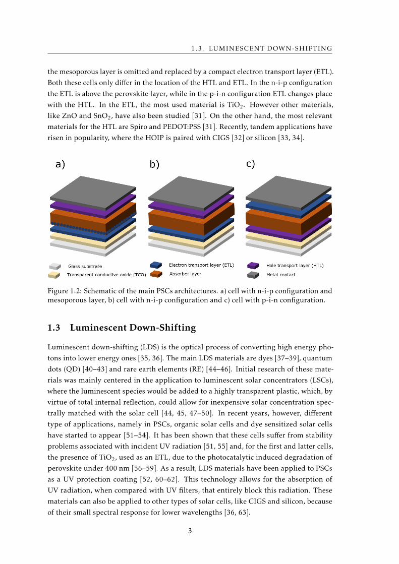
1.3. LUMINESCENT DOWN-SHIFTING
the mesoporous layer is omitted and replaced by a compact electron transport layer (ETL).
Both these cells only differ in the location of the HTL and ETL. In the n-i-p configuration
the ETL is above the perovskite layer, while in the p-i-n configuration ETL changes place
with the HTL. In the ETL, the most used material is TiO2. However other materials,
like ZnO and SnO2, have also been studied [31]. On the other hand, the most relevant
materials for the HTL are Spiro and PEDOT:PSS [31]. Recently, tandem applications have
risen in popularity, where the HOIP is paired with CIGS [32] or silicon [33, 34].
Figure 1.2: Schematic of the main PSCs architectures. a) cell with n-i-p configuration andmesoporous layer, b) cell with n-i-p configuration and c) cell with p-i-n configuration.
1.3 Luminescent Down-Shifting
Luminescent down-shifting (LDS) is the optical process of converting high energy pho-
tons into lower energy ones [35, 36]. The main LDS materials are dyes [37–39], quantum
dots (QD) [40–43] and rare earth elements (RE) [44–46]. Initial research of these mate-
rials was mainly centered in the application to luminescent solar concentrators (LSCs),
where the luminescent species would be added to a highly transparent plastic, which, by
virtue of total internal reflection, could allow for inexpensive solar concentration spec-
trally matched with the solar cell [44, 45, 47–50]. In recent years, however, different
type of applications, namely in PSCs, organic solar cells and dye sensitized solar cells
have started to appear [51–54]. It has been shown that these cells suffer from stability
problems associated with incident UV radiation [51, 55] and, for the first and latter cells,
the presence of TiO2, used as an ETL, due to the photocatalytic induced degradation of
perovskite under 400 nm [56–59]. As a result, LDS materials have been applied to PSCs
as a UV protection coating [52, 60–62]. This technology allows for the absorption of
UV radiation, when compared with UV filters, that entirely block this radiation. These
materials can also be applied to other types of solar cells, like CIGS and silicon, because
of their small spectral response for lower wavelengths [36, 63].
3

CHAPTER 1. INTRODUCTION
1.4 Dielectric Photonic Structures
As stated earlier, the search for highly efficient solar cell technology at low costs is one
of the main drivers for research, with many studies converging in technologies that al-
low smaller cell thickness - less material usage - without compromising optical perfor-
mance. Some examples are the use of light trapping methods, such as metallic or dielectric
nanoparticles on the rear side of the cell [64–66], texturing of the front or rear side of
the cell [67–69] and the use of dielectric structures on top of solar cells [70–73], with the
latter being the one used in this work. This method leads to the enhancement of the cell
absorption due to 2 main reasons. Firstly, by forward scattering light, one can increase
its travel path and, therefore, the likelihood of absorption. Secondly, one can also create
resonant modes, related with the properties of the structures, that can significantly boost
the absorption and, for periodic structures, even surpass the theoretical limit - the Tiedje-
Yablonowitch limit - for specific wavelengths related with the structures’ pitch [67, 74,
75].
1.5 Finite-Difference Time-Domain Simulation
The need for 3D simulation of solar cells with arbitrary geometries has led to the adoption
of the finite-difference time-domain (FDTD) method, that was used in this work. As such,
a brief description of the simulation methodology, based on references [76–78], will be
presented next.
The FDTD method is based on an algorithm derived by Yee in 1966 [78], where
the central difference approximation was applied to both space and time derivatives of
Maxwell’s curl equations to, with a discretization of space and time, create an iterative
process to solve electromagnetic problems, such as the interaction between light and the
solar cell, as used in this work.
The Yee algorithm is based on the Yee cell, shown in Figure 1.3, used to discretize the
simulation space. Each cell has dimensions ∆x, ∆y and ∆z and has its coordinates defined
by the position in the simulation region. Similarly, time is also uniformly discretized as
t = n∆t. As a result, one can express the field functions at any node within the discrete
space. Using the discretization shown in Figure 1.3, it is then possible to approximate
Faraday’s equation via central differences, resulting in Equation 1.1 for the face shown
in the right side of Figure 1.3, representing the approximation for the z component
projection.
µ
Hn+1zi− 1
2 ,j+12 ,k−Hn
zi− 12 ,j+
12 ,k
∆t
=
En+ 1
2xi− 1
2 ,j+1,k+1−En+ 1
2xi− 1
2 ,j,k+1
∆y
−En+ 1
2yi−1,j+ 1
2 ,k+1−En+ 1
2yi,j+ 1
2 ,k+1
∆x
−Mn+ 12
zi− 12 ,j+
12 ,k
(1.1)
4

1.5. FINITE-DIFFERENCE TIME-DOMAIN SIMULATION
Figure 1.3: Schematic representation of the Yee algorithm. On the left is shown the Yeecell with the various corresponding fields. The direction of the fields in each face ischosen to satisfy Faraday’s law. On the right, is shown the field with the full notation,including the spatial coordinates for the top face of the cube.
Using a similar procedure, it is also possible to obtain equivalent equations for the
y and x-projections of Faraday’s law (shown in Annex I). For the next step, one must
create a secondary cell, where the electric and magnetic fields change position, allowing
for a central difference approximation of Ampere’s law, leading to equivalent equations
to that of Equation 1.1. The equation for the x component of Ampere’s law is also shown
in Annex I, with the remaining components obtained in the similar manner to the ones
from Faraday’s law. Lastly, by combining the resulting equations from the last steps, one
ends up with six equations that can be used, together with information of the field at an
initial time, to create a recursive solution scheme to advance the fields through time. In
Annex I these equations, used for the iterative process, are shown, assuming that En+1/2y ,
En+1/2z and Hn
x are known. The Yee algorithm allows for the approximations used to be
second order accurate, meaning the error decreases quadratically with decreasing size of
the Yee cell, allowing for high accuracy results.
When applying this method, one always needs to satisfy the stability criterion, to
avoid divergence of the fields during the calculation. This criterion relates the sizes of
both time and space steps used as shown in Equation 1.2.
∆t <1
vmax
1√1
∆x2 + 1∆y2 + 1
∆z2
(1.2)
The FDTD method is especially suited for this work, since it is a fast and simple
method, that allows the simulation of arbitrarily shaped media, which is of particular
importance when considering photonic structures, as well as inhomogeneous and lossy
media. Lastly, it also allows for broadband frequency simulations, that reduce the simu-
lation time required [67, 70, 76, 77]. In this work, a commercial-grade simulator based
on this method was used [77].
5


Chapter
2Simulation Setup
2.1 Solar Cell Structure
As stated in the previous chapter, this work uses the FDTD method, implemented in the
commercial tool provided by Lumerical Solutions Inc. [77], to study the effects of LDS
on the photo-generated current and generation profiles of PSCs. The schematic for the
cells used in these simulations are shown in Figure 2.1 and the sizes summarized in Table
2.1. The various simulation parameters are described in Annex II. These cells are based
on PSCs optimized to reach maximum photo-generated current. From Chapter 1, one
can see that the materials used are some of the most common in the literature [31]. The
relevant material properties are shown in Annex II.
This work is centered in 2 different cells. First, one will study planar cells, from now
on referred to as PC, shown in Figure 2.1 a) and, secondly, a cell with TiO2 hexagonally
packed voids acting as light trapping structures, from now on called LTC, shown in Fig-
ure 2.1 b). The LTC uses TiO2 since its properties, such as high dielectric constant and low
absorption under 400 nm, make it a promising material for light trapping purposes [70].
For each architecture, 250 nm and 500 nm perovskite thicknesses were considered. The
latter value represents a common optimized thickness for improved trade-off between
opto-electrical performance and the solar cell degradation [15], while the second repre-
sents a common value when considering flexible applications [71, 79]. The LDS material
is generally added to the cell by incorporating it into an encapsulation matrix [52, 60,
63] or by mixing it with the mp-TiO2 used as ETL [54, 61]. For this purpose, only the
first case is considered as it is the easier to simulate. The materials used as encapsulation
are generally highly transparent polymers such as PMMA [52], EVA [63], PVB [63] and
PS [60] with thicknesses in the order of micrometers. As a result, because the FDTD
method is optimized for nanophotonic simulations, an approximation is used where the
7

CHAPTER 2. SIMULATION SETUP
air/encapsulation material reflection was neglected, since it wouldn’t affect the main re-
sults in any meaningful way, and the background index of the simulation was changed to
1.5, which is a common value for these materials [80], case referred from now on as PBI
- polymer background index. For the PC, a simulation with vacuum background index,
from now on referred to as VBI, was still made as a reference.
Table 2.1: PC and LTC parameters. Ag, Spiro and ITO represent the respective materialthicknesses. TiO2, for the PC, represents the TiO2 thickness and for the LTC is the TiO2thickness between perovskite and the structures beginning. tV oids is the structures’ TiO2thickness. R is the voids x and y radius, while Rz is the z radius. tV oids is the distancebetween the center of 2 consecutive void structures, being given in function of R.
Planar Cell (PC) Light Trapping Cell (LTC)
Perovskite thickness (nm) 250 500 250 500
R (nm) - - 401.2 388
Rz (nm) - - 1792 820.8
Pitch (×R) - - 2.2 2.3
ITO (nm) 50 76 63.6 62.3
TiO2 (nm) 20 20 20 93.2
tVoids (nm) - - 656.2 404.6
Spiro (nm) 150 150 150 150
Ag (nm) 80 80 80 80
Figure 2.1: Schematic of the solar cells used in the simulations. a) Cell with planarstructure, PC, used as reference and b) Cell with light trapping structures, LTC. Thedimensions of the cell on the right refer to their respective counterparts in Table 2.1. Thedifferent layers properties are shown in Annex II.
8

Chapter
3Results and Discussion
3.1 Optical simulation
The most important parameters for this work are the absorption, optical photocurrent,
Jph (mA/cm2), and generation rate per unit volume, G (cm−3s−1). The second represents
the maximum current obtainable by the cell, being also a figure of merit related with the
cell’s absorption. The latter represents the generated electrons per unit time through the
entire volume. Considering the electromagnetic theory, one can relate these parameters
with the fields resulting from the simulation and the respective material’s properties [77].
The material’s properties used in this work are provided by reference [80] and are also
ploted in Annex II. Consequently, the absorption per unit volume, Abs (cm−3), can be
calculated using [77]:
Abs = −0.5ω|E|2imag(ε) (3.1)
Where ω is the angular frequency, ε is the material permittivity and |E|2 is the square
modulus of the electric field at the given point in the simulation region. By integrating
the absorption per unit volume to calculate the cell absorption, A(ω), one can then use
the solar spectrum to calculate Jph by the following integral.
Jph =∫A(ω)AM1.5Gdω (3.2)
Where AM1.5G represents the solar spectrum based on the ASTM G-173 global irradi-
ance spectra [16]. This integral is of paramount importance, since the effect of the LDS
layer is considered by changing the spectrum used in the integration, i.e. change AM1.5G.
The generation rate, G, is obtained by the integration of the number of photons per unit
volume, g (J−1cm−3), over the simualtion spectrum. The latter is given by the following
equation: g = Abs~ω
9

CHAPTER 3. RESULTS AND DISCUSSION
3.2 Down Shifted Spectrum
The main objective of this work is to assess the optical effects of using LDS materials
on PSCs by calculating Jph and generation profiles when the cell is shined with a down-
shifted (DS) spectrum. Consequently, the first step is to create a spectrum that would
result from the interaction of the normal AM 1.5G spectrum with the LDS particles. Since
this work does not focus on a particular type of LDS material, but instead, tries to study
the general effect of DS, the setup used to create the shifted spectrum will be an ideal
case that incorporates the main aspects of this process.
Based on emission and absorption profiles measured experimentally from various
research groups for QDs [62, 81], dyes [38, 52, 82] and RE [44, 51], a gaussian profile
was chosen to emulate those spectra as it is the closest shape to the experimental mea-
surements. These gaussian profiles were considered to have unitary amplitude – this
parameter will represent the percentage of photons that are absorbed – a dispersion of 50
nm and the gaussian center, λC , was left as an adjustable parameter for sweeps that will
be shown in a later section. Following the choice of absorption and emission profiles, the
AM1.5G spectrum photon flux, based on ASTM G-173, was employed, together with the
gaussian profile, representing the absorption, to calculate the absorbed flux (blue plot in
Figure 3.1 a)).
The absorbed flux was then shifted to create the emission flux (red plot in Figure 3.1).
The value of this shift was left as a variable for future sweeps. Finally, to simulate the effect
of DS, the AM1.5G spectrum was modified by adding the emission flux and subtracting
the absorption flux. For simplicity, both absorption and emission plots were considered
to be equal and no losses due to effects like isotropic emission of radiation, reabsorption
and non-unitary photoluminescent quantum yield (PLQY) were considered.
Two examples of the resulting power profiles are shown in Figure 3.2. The plot on
the left shows the AM 1.5G spectrum and 2 cases where λC was changed. For lower
wavelengths a reduction of the overall power is observed, depending on the center of
the gaussian profile used. It is also evident that there is a power increase in the region
corresponding to λC plus the shift. On the right, the plot shows the effect of a change
in the shifting parameter, ∆λ, value. Where it can be seen that as ∆λ increases the
peak is redshifted. The irradiance spectra obtained attend to the most important aspects
resulting from the DS process, like lower power for lower wavelengths and analogously
for higher wavelengths as observed by modelled results from Lesyuk et. al. [40, 41], also
shown in Figure 3.1 b).
3.3 Planar Perovskite Solar Cells
Planar cells, introduced in Chapter 2, with different background indexes were first sim-
ulated. The index change represents the switch from the most common simulation en-
vironment – with vacuum background index, VBI – to a background with an index that
10

3.3. PLANAR PEROVSKITE SOLAR CELLS
Figure 3.1: a) In solid line are the absorbed and emitted fluxes for λC of 350 nm and ∆λof 200 nm. In dash line is the gaussian profile used to calculate the absorbed and emittedfluxes; b) Modelled spectra transmitted through a window prototype with varying QDproperties and quantum yield of 50%. Adapted from reference [40]; c) Schematic of theDS process, where higher wavelength radiation is redshifted.
represents the presence of a matrix layer where the LDS particles can be embedded -
polymer background index, PBI. In this second case, the reflection in the interface be-
tween the LDS material matrix and vacuum are not considered, given that these layers
are generally several micrometers thick and, therefore the simulation methodology is
not suited as it would require prohibitive amounts of computer memory. On the other
hand, this reflection effect is ∼4%, which is minimal and thus would not affect the main
results in any significant way. These structures will also allow, due to the lack of photonic
structures that lower the amount of UV absorbing materials, such as TiO2 and ITO, to
check the optical gains of the DS spectrum on a case where there is not a significant UV
parasitic absorption.
3.3.1 Reflection Profiles
Initially, the total reflection and transmission profiles were calculated using the FDTD
method, representing the numerical approximation to the theoretical results, and the
transfer matrix method, obtained from the Fresnel equations for a 1D multistack, repre-
senting the analytical solution. By comparing both these results it is possible to verify the
11

CHAPTER 3. RESULTS AND DISCUSSION
500 1000 1500 20000.0
0.5
1.0
1.5
2.0
500 1000 1500 20000.0
0.5
1.0
1.5
2.0b)Irr
adia
nce
(W/m
2 nm
)
Wavelength (nm)
AM1.5G C = 300, = 310 nm C = 400, = 310 nm
Change in absorption
Power increase
a)
Wavelength (nm)
AM1.5G C = 300, = 205 nm C = 300, = 400 nm
Absorption
Peak change from higher
Figure 3.2: Resulting irradiance plots of the DS process used to simulate the effect of aLDS layer. a) AM1.5G spectrum, in black, and 2 examples of resulting spectrums whenthe ∆λ remains constant as 310 nm and λC changes from 300 nm to 400 nm, in redand blue, respectively, b) AM1.5G spectrum, in black, and 2 examples of the resultingspectrums when λC remains constant at 300 nm and ∆λ varies from 205 nm to 400 nm,in red and blue, respectively.
accuracy of these numerical results.
Reflection profiles have 2 main components, specular reflection, Rs, and difuse reflec-
tion, Rd . The method used for these results calculates the total reflection meaning both
components are considered. However, because the results shown here are for PCs, there
is no Rp, and thus the profiles for the PCs only have a specular component.
The reflection profiles for the 4 simulated PCs are shown in Figure 3.3. The equivalent
transmission results are included in Annex III. From these plots, one can clearly see that
the numerical simulation results make an excellent fit to theoretical curves over the entire
simulation bandwidth. The inset profiles show the difference between the reflection
values of the numerical simulation and theoretical results, validating the simulation
method used as the difference is always inferior to 9× 10⁻³.
Considering the optical information shown in these graphs, one notices immediately
the high reflection for wavelengths above 700 nm. When the cell thickness is increased,
this effect is attenuated, as shown in Figure 3.3 b) and d) by the small dip around 900 nm.
This effect results from Fabry Perot-like interference patterns arising from constructive
interference of the propagating light [70]. However, the reflection, for the most part is
still significative, reaching values up to 80%. Consequently, there is a need to create
mechanisms to trap light and improve these losses, as will be further expanded later.
On the other side of the spectrum, under 700 nm, one can see the considerable low
reflection, mainly attributed to the use of ITO as an anti-reflection coating. From Fresnel’s
equations it is known that smaller differences in material’s refractive index, on an inter-
face, leads to lower reflection. Considering ITO’s index of 1.9, together with perovskite
12

3.3. PLANAR PEROVSKITE SOLAR CELLS
0.3 0.4 0.5 0.6 0.7 0.8 0.9 1.00.0
0.2
0.4
0.6
0.8
1.0
0.3 0.4 0.5 0.6 0.7 0.8 0.9 1.00.0
0.2
0.4
0.6
0.8
1.0
0.3 0.4 0.5 0.6 0.7 0.8 0.9 1.00.0
0.2
0.4
0.6
0.8
1.0
0.3 0.4 0.5 0.6 0.7 0.8 0.9 1.00.0
0.2
0.4
0.6
0.8
1.0
Ref
lection
FDTD Theoretical
0.4 0.6 0.8 1.00.000
0.003
0.006
0.009
R|
d)c)
b)a)
0.4 0.6 0.8 1.00.000
0.002
0.004
0.006
R|
Ref
lection
Wavelength ( m)
0.4 0.6 0.8 1.00.000
0.002
0.004
0.006
|R|
Wavelength ( m)
0.4 0.6 0.8 1.00.000
0.002
0.004
0.006
|R|
Figure 3.3: Reflection profiles with the results from the numerical simulation, in black,and the results from the theoretical simulation, in red. Inset is represented the modulusof the difference between the two methods. a) PC with 250 nm perovskite, b) PC with500 nm perovskite, c) PC with background index of 1.5 and 250 nm perovskite, d) PCwith background index of 1.5 and 500 nm perovskite.
or TiO2’s index of 2.5 (under 700 nm) [80], a lower reflection would indeed be expected,
when compared with the vacuum index. This optical matching effect also explains the
difference between the reflection under 700 nm for the VBI case (Figure 3.3 a) and b)) and
the PBI case (Figure 3.3 c) and d)), since the latter provides a smaller index difference,
when compared to ITO. In fact, due to the similar refractive index of the background and
ITO, there are some points where the observed reflection is nearing 0% (ideal matching
case).
3.3.2 Absorption Profiles
The absorption profiles were calculated as described in Section 3.1, by integrating the
absorbed power per unit volume, and are displayed in Figure 3.4. These plots have 4
main components: the absorption due to the perovskite layer, curve in black; the TiO2
layer, represented by the red shaded part; the remaining materials in the cell (ITO and
Spiro), illustrated by the green shaded part. The last components are the inset profiles
showing the absorbed power density throughout the cell for specific wavelengths, namely
350 and 900 nm. The first component is of paramount importance, as it represents the
13

CHAPTER 3. RESULTS AND DISCUSSION
absorption that will lead to the production of energy. The second component, due to
TiO2 being the main UV absorber in the cell, will also be very important to analyze the
optical gains from the shifted spectrum. The third simply represents the general parasitic
absorption. However, it should be noted that ITO also has parasitic absorption leading
to photocurrent gains. The last component, the inset profiles, exhibit the absorption
behavior for different wavelengths.
Because the transmition values, shown in Annex III, are negligeable, the absorption
can be calculated from the reflection using A = 1 − R, where R is the reflection from
the previous subsection, meaning that both these parameters are intimately related. For
most of the simulation bandwidth the 500 nm cells – Figure 3.4 b) and d) – show higher
absorption than its 250 nm counterpart – Figure 3.4 a) and c) – since in the former light
will have a higher travel path. In the last subsection it was discussed that the PBI cells’
reflection for wavelengths under 700 nm lowered around 10%, when compared with
the VBI cells. This effect is also enhanced in these plots where the cell has better index
matching. Also present in these graphs is the lower absorption for wavelengths above
800 nm, that will be further analyzed in a later section, when the LTCs are introduced.
A relevant aspect present is the TiO2’s parasitic UV absorption - reaching values
between 10-20% under 400 nm - where the TiO2 is optically active. Despite the TiO2
reduced thickness, these values are still significant and impact perovskite’s absorption
in these wavelengths. As will be shown in a later section, the increase in TiO2 thickness
will lead to a further decrease in perovskite absorption due to higher absorption of this
material, completely blocking the UV radiation from reaching the absorber.
For the remaining materials, in the most energetic section of the spectrum, the ab-
sorption is mainly attributed to the ITO layer, as it is the first one in the cell, reaching
values up to 20%. These absorption figures are corroborated by the inset profiles with the
absorbed power for 350 nm, where it can be seen that Spiro’s absorption is almost negli-
gible, being ITO and TiO2 the second higher absorbers, after perovskite. Consequently,
it is expected that, with the use of a LDS material to change the incident spectrum, one
will be able to mitigate the unwanted electron generation in these layers, shifting the
photo-generation to the absorber layer.
For higher wavelength photons, there is parasitic absorption from both Spiro and
ITO. From the inset profiles on the right, that show the absorbed power for 900 nm, one
can see that these materials can reach similar absorption values to those of perovskite.
Although this study is not the main focus of this work, it is also important to note that by
reducing these parasitic absorptions and, therefore, increasing perovskite’s absorption,
one can increase the cell’s Jph, as shown in recent works by Mendes et.al. [70, 71]. From
the standard AM 1.5G spectrum, shown in Section 3.2, it can be seen that there is still
some relevant radiation for wavelengths above 800 nm.
Considering the absorption values above 80% for wavelengths ranging from 400 to
750 nm, the excellent absorption properties of perovskite are seen. Several equivalent
studies, for amorphous silicon (a-Si) solar cells [70, 74], crystalline silicon cells [70], CIGS
14

3.3. PLANAR PEROVSKITE SOLAR CELLS
cells [64] and even GaAs cells [68], show lower absorption for an equivalent wavelength
range, when compared with perovskite’s. These outstanding absorption properties make
perovskite a very compelling material for solar cells and this is, to some extent, part of
the reason they are so widely studied.
Perovskite + TiO2 Perovskitea)
Abso
rptio
n
Wavelength ( m)
-0.2 -0.1 0.0 0.1 0.20.1
0.2
0.3
0.4
0.5
z (
m)
x ( m)1.0x10⁻²
1.4x100
1.9x10²
7.0x10³Pabs (x1016 cm-3)
ITOTiO2
Perovskite
Spiro-0.2 -0.1 0.0 0.1 0.2
0.2
0.4
0.6
0.8
z (
m)
x ( m)1.0x10⁻⁴
6.7x10⁻²
4.4x101
5.0x10³Pabs (x1016 cm-3)
ITOTiO2
Perovskite
Spiro
-0.2 -0.1 0.0 0.1 0.2
0.2
0.4
0.6
0.8
z (
m)
x ( m)1.0x10⁻⁴
8.6x10⁻²
7.4x101
1.0x10⁴Pabs (x1016 cm-3)
ITOTiO2
Perovskite
Spiro
Wavelength ( m)
Figure 3.4: Absorption profiles with the absorption on the perovskite layer, in black; theTiO2 layer, in red; and the total cell absorption, in green. The inset profiles show theplots for the absorbed power density through the cell volume for specific wavelengths,indicated by the arrows. The leftmost graph is the absorbed power for 350 nm and therightmost graph is the absorbed power for 900 nm. a) and b) PC with VBI for 250 nm and500 nm perovskite, respectively; c) and d) PC with PBI for 250 nm and 500 nm perovskite,respectively.
3.3.3 Photocurrent Shifts
Together with the solar spectrum, the calculated absorption profiles, can be employed to
obtain the maximum value of photocurrent in the cell, as described in Section 3.1. These
values act as a figure of merit of the optical performance of the cell and, therefore can be
used to compare different cell architectures.
By integrating different spectrums, using the process shown earlier in Figure 3.1, one
can emulate the effect on Jph of having an LDS material on top of the cell. Consequently,
a sweep was made, where λC was varied between 300 and 400 nm and ∆λ between 100
15

CHAPTER 3. RESULTS AND DISCUSSION
25.94
26.29
22.87
23.03
100
150
200
250
300
350
400
(nm
)
24.00
24.37
24.74
25.12
25.50
25.89
26.29Jph (mA/cm2)
300 320 340 360 380 400100
150
200
250
300
350
400b)
C (nm)
(nm
)
20.60
20.99
21.38
21.78
22.19
22.60
23.03Jph (mA/cm2)
a)Jph sweeps for PCs with VBI
Figure 3.5: Contour plots for the sweeps where λC and ∆λ were varied from 300 nmto 400 nm and 100 nm to 400 nm, respectively. a) PC with VBI for 500 nm perovskitelayer and b) PC with VBI for 250 nm perovskite layer. The thicker line represents thecontour corresponding to the photocurrent value obtained for the pristine spectrum. Theindicated values represent the respective contour photocurrent value. The topmost valuerefers to the contour representing the pristine value, while the bottommost refers to thehighest value contour in the plot.
16

3.3. PLANAR PEROVSKITE SOLAR CELLS
26.96
27.20
24.32
24.45
300 320 340 360 380 400100
150
200
250
300
350
400a)
(nm
)
24.70
25.10
25.51
25.92
26.34
26.77
27.20Jph (mA/cm2)
b)
300 320 340 360 380 400100
150
200
250
300
350
400
Jph sweeps for PCs with PBI
C (nm)
(nm
)
21.40
21.88
22.37
22.87
23.39
23.91
24.45Jph (mA/cm2)
Figure 3.6: Contour plots for the sweeps where λC and ∆λ were varied from 300 nmto 400 nm and 100 nm to 400 nm, respectively. a) PC with PBI for 500 nm perovskitelayer, b) PC with PBI for 250 nm perovskite. The thicker line represents the contour cor-responding to the photocurrent value obtained for the pristine spectrum. The indicatedvalues represent the respective contour photocurrent value. The topmost value refers tothe contour representing the pristine value, while the bottommost refers to the highestvalue contour in the plot.
17

CHAPTER 3. RESULTS AND DISCUSSION
and 400 nm. The resulting plots are shown in Figure 3.5 for the VBI cell and in Figure
3.6 for PBI cell.
In all cases, the trend when both parameters change is similar and give a general idea
of how the changing spectrum can influence the maximum current output. When con-
sidering ∆λ above 250 nm, Jph drops steadily to a minimum, reaching values 2 mA/cm2
lower than the pristine value, shown by the thicker line in the different plots. The absorp-
tion profiles from the last section show that, above 800 nm there is a significant reduction
in the cell absorption, associated with the perovskite bandgap, ∼1.55 eV, used for these
simulations. Consequently, when the ∆λ is significantly increased, the spectrum gets
redshifted, Figure 3.1, to where the cell has lower performance negatively impacting its
optical response.
In Table 3.1 the Jph for the pristine and optimized spectrums are summarized, to-
gether with their absolute and relative differences. Here it is seen that the differences are
small, with a maximum of 0.35 mA/cm2(1.3%) for the VBI cell with 500 nm perovskite.
The thin TiO2 layer used in these cells is the main factor inhibiting this increase as it
is the main UV absorber before perovskite. This lower parasitic absorption is optically
advantageous, as it allows for an increase in perovskite’s absorption. However, practi-
cally, it has some issues related with the UV degradation of MAPbI3. Several reports
have studied the degradation mechanisms, but the full picture hasn’t yet been totally
understood. Nonetheless, one of the points of focus has been the creation of I2 that leads
to the structural decomposition of perovskite’s crystal [55, 57]. This can appear at the
TiO2/perovskite interface from TiO2’s catalytic effects [57] and from the known photol-
ysis of PbI2 present in the perovskite’s structure [55]. Therefore, on one side, the UV
shading of the cell produced by a thicker layer of TiO2 could be seen as beneficial, reduc-
ing this degradation in detriment of the photocurrent that would be generated otherwise.
However, considering TiO2’s photocatalytic effects under 400 nm the use of either a UV
filter or LDS are preferred to avoid perovskite’s degradation, with the latter enabling the
reabsorption of the otherwise lost radiation [52].
The optimized ∆λ and λC values for the Jph from Table 3.1 are summarized in Table
3.2. Adding these values, the result varies between 400 to 500 nm, representing the
wavelengths to where the spectrum is shifted. Given that these values depend heavily
on the device absorption, which is more prevalent in the 400-700 nm range (Figure 3.4),
these results were expected.
3.3.4 Generation Profiles and UV absorption
The generation profiles were calculated, as explained in Section 3.1, for the pristine
spectrum and the one corresponding to the optimized ∆λ and λC values, shown in Section
3.3.3. The results for the PCs with VBI are shown in Figure 3.7 and, for the cells with PBI,
in Figure 3.8. For all cases in study, the main difference is the reduction of the harmful
photo-generation in the TiO2 layer. This value varied from around 2 × 1026cm−3s−1 to
18
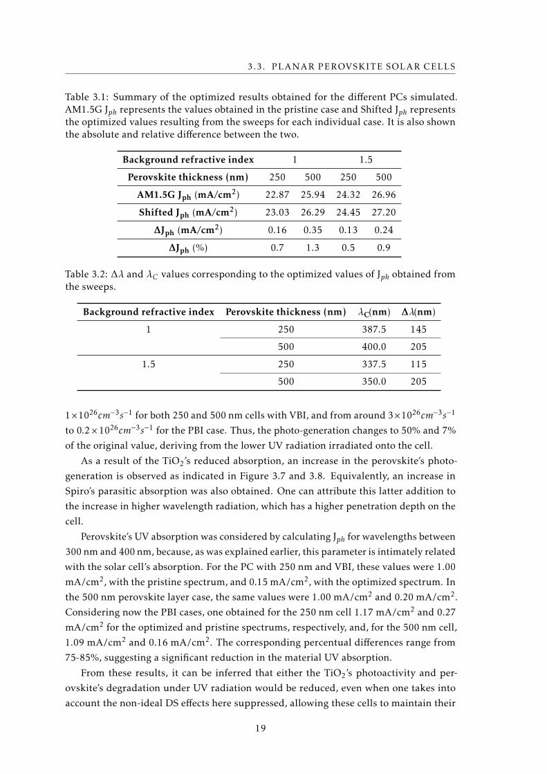
3.3. PLANAR PEROVSKITE SOLAR CELLS
Table 3.1: Summary of the optimized results obtained for the different PCs simulated.AM1.5G Jph represents the values obtained in the pristine case and Shifted Jph representsthe optimized values resulting from the sweeps for each individual case. It is also shownthe absolute and relative difference between the two.
Background refractive index 1 1.5
Perovskite thickness (nm) 250 500 250 500
AM1.5G Jph (mA/cm2) 22.87 25.94 24.32 26.96
Shifted Jph (mA/cm2) 23.03 26.29 24.45 27.20
∆Jph (mA/cm2) 0.16 0.35 0.13 0.24
∆Jph (%) 0.7 1.3 0.5 0.9
Table 3.2: ∆λ and λC values corresponding to the optimized values of Jph obtained fromthe sweeps.
Background refractive index Perovskite thickness (nm) λC(nm) ∆λ(nm)
1 250 387.5 145
500 400.0 205
1.5 250 337.5 115
500 350.0 205
1×1026cm−3s−1 for both 250 and 500 nm cells with VBI, and from around 3×1026cm−3s−1
to 0.2×1026cm−3s−1 for the PBI case. Thus, the photo-generation changes to 50% and 7%
of the original value, deriving from the lower UV radiation irradiated onto the cell.
As a result of the TiO2’s reduced absorption, an increase in the perovskite’s photo-
generation is observed as indicated in Figure 3.7 and 3.8. Equivalently, an increase in
Spiro’s parasitic absorption was also obtained. One can attribute this latter addition to
the increase in higher wavelength radiation, which has a higher penetration depth on the
cell.
Perovskite’s UV absorption was considered by calculating Jph for wavelengths between
300 nm and 400 nm, because, as was explained earlier, this parameter is intimately related
with the solar cell’s absorption. For the PC with 250 nm and VBI, these values were 1.00
mA/cm2, with the pristine spectrum, and 0.15 mA/cm2, with the optimized spectrum. In
the 500 nm perovskite layer case, the same values were 1.00 mA/cm2 and 0.20 mA/cm2.
Considering now the PBI cases, one obtained for the 250 nm cell 1.17 mA/cm2 and 0.27
mA/cm2 for the optimized and pristine spectrums, respectively, and, for the 500 nm cell,
1.09 mA/cm2 and 0.16 mA/cm2. The corresponding percentual differences range from
75-85%, suggesting a significant reduction in the material UV absorption.
From these results, it can be inferred that either the TiO2’s photoactivity and per-
ovskite’s degradation under UV radiation would be reduced, even when one takes into
account the non-ideal DS effects here suppressed, allowing these cells to maintain their
19

CHAPTER 3. RESULTS AND DISCUSSION
performance figures for a longer time period. Later, this point will be further expanded
for the LTC. It can also be added that a small reduction in the ITO layer photo-generation
was also achieved.
-0.2 -0.1 0.0 0.1 0.20.1
0.2
0.3
0.4
0.5
d)
z (
m)
ITOTiO2
Perovskite
Spiro
-0.2 -0.1 0.0 0.1 0.2c)
b)
0.8
1.9
4.6
11.0
26.2
62.7
150.0Generation (x1026 cm-3s-1)a)
-0.2 -0.1 0.0 0.1 0.2
0.15
0.30
0.45
0.60
0.75
Spiro
Perovskite
TiO2ITO
z (
m)
x ( m)-0.2 -0.1 0.0 0.1 0.2
x ( m)0.8
1.9
4.6
11.0
26.2
62.7
150.0
Figure 3.7: Generation profiles for the PCs with VBI. a) cell with 250 nm perovskite; b)cell with 250 nm perovskite and optimized spectrum; c) cell with 500 nm perovskite; d)cell with 500 nm perovskite and optimized spectrum. The arrows and ellipse mark thebiggest changes in the plots.
3.4 Solar Cells with Dielectric Photonic Structures
In this section, the focus is in the cells with photonic structures. As stated earlier, PC
performance suffers from significant losses associated with lower absorption for higher
wavelengths, paving the way for the development of different methods to mitigate these
losses.
In this work, high dielectric constant structures are considered for use on top of solar
cells to act as forward scatterers of light, causing an increase of its travel path, and,
consequently, their chance of being absorbed [72, 74]. The use of these structures can also
lead to the creation of localized modes in the absorber material that will then increase
20

3.4. SOLAR CELLS WITH DIELECTRIC PHOTONIC STRUCTURES
-0.2 -0.1 0.0 0.1 0.20.1
0.2
0.3
0.4
0.5
z (
m)
ITOTiO2
Perovskite
Spiro
-0.2 -0.1 0.0 0.1 0.20.1
0.3
1.1
3.9
13.1
44.3
150.0Generation (x1026 cm-3s-1)
-0.2 -0.1 0.0 0.1 0.2
0.15
0.30
0.45
0.60
0.75
z (
m)
x ( m)
ITO TiO2
Perovskite
Spiro-0.2 -0.1 0.0 0.1 0.2
c) d)
b)
x ( m)0.2
0.6
1.8
5.5
16.5
49.8
150.0
a)
Figure 3.8: Generation profiles for the PCs with PBI. a) cell with 250 nm perovskite; b)cell with 250 nm perovskite and optimized spectrum; c) cell with 500 nm perovskite; d)cell with 500 nm perovskite and optimized spectrum. The arrows and ellipse mark thebiggest changes in the plots.
the absorption due to the high intensity electric fields generated [72].
For this method, the format of the structures is rather important given that, according
to the Fresnel’s equations, the reflection increases for steeper refractive index changes.
As a result, various studies were conducted, where different structures were tested to
assess which one had the best optical performance [71]. The material used for these
structures was TiO2, because of its low parasitic absorption for wavelengths above 400
nm and its high dielectric constant (around 2.5) [70]. The use of this material in silicon
solar cells does not result in any significant photocurrent losses as, in TiO2 photoactive
zone, silicon has a low absorption so TiO2’s parasitic absorption does not impact the cell
performance. However, when considering perovskite, the degrading effects of TiO2’s
photoactivity should be taken into account. As such, part of this section is centered in
the effects of using an LDS material to minimize the absorption in the TiO2 layer, that, in
practice, should result in a lower degradation of the perovskite material.
21

CHAPTER 3. RESULTS AND DISCUSSION
3.4.1 Reflection Profiles
In Figure 3.9 are shown the plots for the simulated reflection of both PC with PBI, and
LTC for 250 nm and 500 nm perovskite layers. Contrary to the PCs, this reflection is
composed of a specular and a diffuse part due to the photonic structures envolved.
For the low wavelengths part of the spectrum, there is no significant change in the
reflection, due to the good index matching between the background and ITO layer. It
should be noted that, under 350 nm, a spike in reflection occurs, related with an increase
in ITO’s refractive index that reaches values up to 2.4 [80]. This spike is somewhat
mitigated by employing photonic structures as they provide a better matching between
the background and ITO.
The focal point to take into account here is the lower reflection for higher wavelengths,
stemming from the use of photonic structures. It should be noted that the dips occurring
above 800 nm, evidenced in the reflection profiles, arise from localized modes that are
created inside the absorber material leading to a significant increase in the cell absorption.
These modes are observed and discussed in the following section.
0.3 0.4 0.5 0.6 0.7 0.8 0.9 1.00.0
0.2
0.4
0.6
0.8
1.0
0.3 0.4 0.5 0.6 0.7 0.8 0.9 1.00.0
0.2
0.4
0.6
0.8
1.0b)
Reflection
Wavelength ( m)
Planar Dielectric Structures
Light trappingenhancements
a)
Wavelength ( m)
Light trappingenhancements
Figure 3.9: a) Reflection profile for the LTC, in black; and for the PC, in red; where bothhave a 250 nm layer of perovskite absorber material. b) Reflection profile for the LTC, inblack; and for the PC, in red; where both have a 500 nm perovskite absorber material.
3.4.2 Absorption Profiles
Similarly to the last section, the next step consists in the calculation of the absorption
profiles due to their important relation with the photocurrent parameter, used to char-
acterize the optical performance of the cell. Again, the A = 1 − R relation is seen. In
Figure 3.10 are shown the absorption profiles obtained for LTC with the absorption of
the perovskite absorber, TiO2 and remaining materials distinguished by color. Inset are
also shown 2 contour plots of the absorbed power density for 350 nm, bottom graph and
900 nm, top graph.
22

3.4. SOLAR CELLS WITH DIELECTRIC PHOTONIC STRUCTURES
At a first glance, comparing with the previous PC results (Figure 3.4), one immedi-
ately notices the significant increase in TiO2’s absorption. Previously, for wavelengths
ranging from 300 nm to 400 nm, results were around 10-20%, while, in this case, they
rose to values between 60-80%, representing a shading of the absorber material for this
wavelengths range. The main reason leading to this change is the thicker TiO2 layer used,
as predicted by the Beer-Lambert law. Considering the absorbed power density plots
for 350 nm, one can also see this effect, since TiO2 represents the majority of absorbed
power by the cell. Consequently, one will expect that the effect of changing the incident
spectrum will lead to an overall increase in the photocurrent generated by the cell.
An increased absorption of low energy photons is observed, reminiscent of the local-
ized modes created inside the absorber material, consequence of the photonic structures
employed. An example of these modes can be seen in the 900 nm wavelengths inset
plots (top plots) in Figure 3.10, deriving from the different interferences generated by the
interaction of light with the structures, consequently leading to the significant increase
of the cell absorption.
Comparing the absorption of the remaining materials, namely ITO and Spiro, shown
by the green shaded zone in the plots, with their equivalent absorption for the PCs. For
wavelengths between 400 and 700 nm the absorption increases minimally from 1-3% to
3-4%. Under 400 nm this absorption went from 10-20% to 20-30%. While, above 700
nm it increased from 4-5% to 8-10%. These overall trends are related with the structures
employed, as the increased surface area to improve the index matching between the
background and the cell, also leads to higher overall parasitic absorption.
3.4.3 Photocurrent Shifts
Analogous to the PCs, sweeps were performed, where the λC and ∆λ, for the LDS ma-
terials, were varied between 300 nm to 400 nm and 100 nm to 400 nm, respectively,
to emulate the shifted spectrum as described in Figure 3.1. The results are shown in
Figure 3.11 and the optimized values, along with their corresponding ∆λ and λC , are
summarized in Table 3.3 and 3.4, respectively.
The main aspect resulting from these plots, when compared to the PCs, is the higher
increase in Jph when the DS spectrum is applied. The PCs saw increases shy of 1% while,
in this case, the increase was ∼2%. This improvement is linked to the higher TiO2 ab-
sorption, associated with the increased thickness, as evidenced by the absorption plots
from Figure 3.4, for the PC, and Figure 3.10, for the LTC. While a 2% increase may seem
as small, it should be noted that, the maximum gain attainable, by absorbing the entire
AM1.5G spectrum for wavelengths between 300 nm and 400 nm, is 1.35 mA/cm2 (value
calculated from the integration of the solar flux for the indicated range). Considering
the different absorption plots shown throughout this work, the outstanding perovskite
absorption under 700 nm is one of its most eye-catching features. As such, and under-
standably, introducing LDS as a manner to significantly increase Jph, ends up falling short
23

CHAPTER 3. RESULTS AND DISCUSSION
Perovskite+TiO2 Perovskite
-0.4 -0.2 0.0 0.2 0.4
0.3
0.6
0.9
1.2
z (
m)
x ( m)1.0x10⁻³
1.2x10⁻¹
1.5x101
5.0x10²Pabs (x1016 cm-3)
-0.4 -0.2 0.0 0.2 0.4
0.3
0.6
0.9
1.2
z (
m)
x ( m)1.0x10⁻⁵
6.7x10⁻³
4.4x100
5.0x10²Pabs (x1016 cm-3)
Wavelength ( m)
a)
Figure 3.10: a) Absorption profile for the LTC with 250 nm perovskite layer, b) absorp-tion profiles for the LTC with 500 nm perovskite layer. The shaded areas represent theabsorption of the TiO2, in red; and the remaining materials absorption, in green. Theblack curve is the perovskite absorption. The inset plots represent the absorbed powerdensity for each respective cell for a wavelength of 350 nm, bottom graph, and 900 nm,top graph.
on major performance improvements, even when considering the ideal case here used for
the shifting process. It should be noted that, the main objective of this method is to avoid
the stability hindering TiO2 photo-generation and harmful perovskite UV absorption
without negatively impacting these cell’s optical performance. Furthermore, given the
optical nature of these studies, electrical phenomenon such as recombination are not con-
sidered which, in their own terms, can also benefit from lower UV radiation and higher
visible radiation [53].
Table 3.3: Optimized Jph results of the λC and ∆λ sweep done. It’s shown the pristineresults, AM1.5G Jph; the results corresponding to the maximum value obtained from thesweep, Jph; and the absolute and relative difference between both values ∆Jph.
Perovskite thickness (nm) 250 500
AM1.5G Jph (mA/cm2) 26.09 28.07
Shifted Jph (mA/cm2) 26.66 28.62
∆Jph (mA/cm2) 0.57 0.55
∆Jph (%) 2.2 2.0
Similarly, to the PC, for higher ∆λ and λC , the cell’s optical current suffers a steep
decrease. Taking the example of the 250 nm cell (Figure 3.11 b)), the pristine value, shown
in the plots by a thicker line, is 26.09 mA/cm2. For a ∆λ and λC of 400 nm a Jph value
under 24.3 mA/cm2 is observed, representing a decrease of almost 7%. Consequently,
24

3.4. SOLAR CELLS WITH DIELECTRIC PHOTONIC STRUCTURES
28.07
26.09
300 320 340 360 380 400100
150
200
250
300
350
400
Jph sweeps for LTC
26.66
b)
(nm
)
26.50
26.84
27.19
27.54
27.89
28.25
28.62Jph (mA/cm2)a)
28.62
300 320 340 360 380 400100
150
200
250
300
350
400
C (nm)
(nm
)
24.30
24.68
25.06
25.45
25.85
26.25
26.66Jph (mA/cm2)
Figure 3.11: Contour plots for the sweeps where λC and ∆λ were changed from 300 nmto 400 nm and 100 nm to 400 nm, respectively. a) Plot for the cell with 250 nm perovskitelayer and b) plot for the cell with 500 nm perovskite layer. The thicker line representsthe contour corresponding to the photocurrent value obtained for the pristine spectrum.The indicated values represent the respective contour photocurrent value. The topmostvalue refers to the contour representing the pristine value, while the bottommost refersto the highest value contour in the plot.
25

CHAPTER 3. RESULTS AND DISCUSSION
the use of suboptimal shifting and absorption properties of DS materials can significantly
hinder the cell performance, as evidenced by the redshifting (Figure 3.1 a)) to wavelengths
where the cell shows worse absorption (Figure 3.10).
Considering the optimal ∆λ and λC values. One can see that the λC leading to im-
proved optical performance is 350 nm for both cases, which resembles the behavior pre-
viously verified for the PCs with PBI. This result is expected, as these photonic structures
mainly affect the absorption for higher wavelength photons, that are not significantly
affected by LDS particles. On the other hand, ∆λ tends to fluctuate between each case.
For these cells, ∆λ changes from 130 nm for the 250 nm cell to 190 nm for the 500 nm
cell. However, when considering the photocurrent shift plots, the difference is mainly
irrelevant as it represents changes under 0.1%. One should also note that the maximum
photocurrent is obtained when the spectrum is shifted to around 500 nm, which is of
particular importance, as electrically, the external quantum efficiency measured for these
cells tends to have a maximum near this point [13, 52, 53, 61].
Table 3.4: ∆λ and λC , values corresponding to the optimum Jph values. The values on theleft represent the thickness of the perovskite used in the cell simulation.
Perovskite thickness (nm) λC (nm) ∆λ (nm)
250 350 130
500 350 190
3.4.4 Generation Profiles
This study was finalized by calculating the generation profile for the LTC, whose plots
are shown in Figure 3.12. The left plots represent the pristine generation profiles, while
the right plots represent the generation with the optimized spectrum discussed in the
last subsection. The most notable aspect is the significant reduction in the TiO2 photo-
generation with the spectral change. For the 250 nm cell, in the evidenced part of the
plot, the photo-generation decreased from 0.42× 1026 to 0.03× 1026 mA/cm2. The 500
nm cell, suffered a similar decrease from 0.16 × 1026 mA/cm2 to 0.03 × 1026 mA/cm2,
representing reductions of one order of magnitude in the harmful TiO2 photo-generation.
These results are equivalent to those of the PC, although in this case the higher TiO2
thickness helps understand the reduction better.
As pointed out in the generation profiles of Figure 3.12, a small decrease in the gen-
eration peak, located in the perovskite’s top corners, is observed. This reduction is a
consequence of the UV spectrum redshift, where light has a higher penetration depth
and, therefore, instead of highly concentrated absorption near the absorber material top
interface, there is a more delocalized absorption throughout the absorber volume. This
effect can be electrically favorable for the cell as there is less surface absorption and,
consequently, less recombination.
26

3.5. FINAL THOUGHTS
-0.4 -0.2 0.0 0.2 0.4
0.2
0.4
0.6
0.8
1.0
1.2
PerovskitePerovskite
Perovskite
z (
m)
Perovskite
-0.4 -0.2 0.0 0.2 0.4d)c)
b)
0.03
0.12
0.49
1.97
7.97
32.20
130.00Generation (x1026 cm-3s-1)a)
-0.4 -0.2 0.0 0.2 0.4
0.2
0.4
0.6
0.8
1.0
1.2
z (
m)
x ( m)-0.4 -0.2 0.0 0.2 0.4
x ( m)0.01
0.06
0.31
1.73
9.65
53.82
300.00
Figure 3.12: Generation profiles for the LTC. a) cell with 250 nm perovskite; b) cell with250 nm perovskite and optimized spectrum; c) cell with 500 nm perovskite; d) cell with500 nm perovskite and optimized spectrum. The arrows point to the biggest plot changes.
Similar to Subsection 3.3.4, an evaluation of the perovskite’s UV absorption was made
by calculating Jph for these different cases. The values obtained for the LTC with 250 nm
perovskite were 0.68 mA/cm2 and 0.13 mA/cm2 for the pristine and optimized spectra,
respectively, while the LTC with 500 nm perovskite saw a reduction from 0.73 mA/cm2
to 0.13 mA/cm2. The above-mentioned values represent reductions ∼80%, which is
very similar to those of the previously studied PCs. Therefore, an important decrease
in perovskite’s UV absorption was obtained. Granted, the simulation methodology here
employed does not attend to all intricacies of the DS process, however, these results
demonstrate some interesting general results coming from the adoption of these materials
on PSCs that could improve the device’s life-span. In fact, recent studies from different
research groups, have used LDS materials on PSC’s to achieve a better life-span [60–62].
One example, by Anizelli et. al., even compared the results against a UV filter obtaining
equivalent long-term values for the cell parameters [52].
3.5 Final ThoughtsTo summarize the fundamental results from this work, a bar chart was made, where the
Jph improvements and UV absorption reductions are shown (Figure 3.13).
27

CHAPTER 3. RESULTS AND DISCUSSION
Starting with the photocurrent chart (Figure 3.13 a)). A first point to be made is the
higher current for the 500 nm cells, resulting from the thicker absorber. This difference
is reminiscent of higher VIS-NIR radiation absorption, as demonstrated in Figure 3.4 for
the PC and Figure 3.10 for the LTC. Secondly, the higher for the PBI PC, when compared
with VBI PC, that stems from better index matching between the background and the
first material in the cell (ITO), as seen in Figure 3.4. The 500 nm cell, for the PBI case, can
even come close to the LTC with 250 nm. However, it should be noted that the dimensions
here used for the LTC were based on optimizations done for a VBI case. Consequently,
the VIS-NIR absorption improvements are not as high as they should be in its optimized
application.
A last analysis of this graph also indicates small current increases when using the
optimized spectrum. Considering these studies were made without any losses, Figure 3.1
a), it can be inferred that these materials do not show a pronounced increase in optical
performance. However, electrical effects, that were not considered in this work, like bulk
instead of surface absorption and lower thermal losses that come with higher energy
transitions, can be deciding factors leading to improved cell current.
Considering now the bar chart analyzing the UV Jph. As referred in earlier sections,
this parameter is indicative of the overall cell absorption for the selected range. Con-
sequently, by calculating this value between 300 nm and 400 nm, one can assess the
UV absorption of these cells. From the chart, a reduction around 80% is observed for
all cases. This constitutes a major reduction in the perovskite’s absorption, even when
one considers the idealized DS case here employed. Therefore, by maintaining a similar
optical current, while significantly reducing the harmful effects of UV radiation in these
cells, one would expect an increased long-term performance.
PC PC PC PC LTC LTC10
15
20
25
30 Optimized spectrum Pristine spectrum
28.0
728
.62
26.0
926
.66
27.2
026
.96
24.4
524
.3226
.29
25.9
4
23.0
3
J ph
(mA/
cm2 )
n = 1 n = 1.5
250 500 250 500 250 500
22.8
7
PC PC PC PC LTC LTC0.0
0.3
0.6
0.9
1.2
b)
82%
81%
85%
76%
80%
n = 1.5n = 1
UV
J ph
(mA/
cm2 )
250 500 250 500 250 500
85%
a)
Figure 3.13: a) Bar chart summarizing the pristine (red) and optimized (blue) Jph valuesobtained from the photocurrent sweeps; b) Bar chart summarizing the Jph for wavelengthsranging from 300 nm to 400 nm for the for the pristine (red) and optimized spectrum(blue).
28

Chapter
4Conclusion and Future Perspectives
A theoretical study on the viability of applying LDS particles to reduce PSC’s UV degrada-
tion was made. The findings here discussed are in accordance with those experimentally
accomplished in recent literature.
The use of these materials did not reveal a pronounced increase in photocurrent, as
was seen by the photocurrent sweeps done (subsections 3.3.3 and 3.4.3). Here, the max-
imum change is ∼2% for the cells with photonic structures and 1% for the planar cells,
with the main difference being attributed to the lower TiO2 thickness of the latter. On
the other hand, the use of unoptimized ∆λ and λC can severely impact the optical perfor-
mance of the cell, reducing the photocurrent by 7%, for the worst cases simulated. The
optimum ∆λ and λC implied a spectrum shift to wavelengths around 500 nm, blending
well with the PSC’s electrical performance peak.
Importantly, from the performed analysis related with perovskite stability, one ob-
tained a significant reduction in TiO2 harmful photo-generation of one order of magni-
tude, coupled with an increase in perovskite bulk generation (Figure 3.7, 3.8 and 3.12).
By assessing the perovskite UV photocurrent for the different simulated cells, reductions
∼80% were obtained when comparing Jph values for the pristine and changed spectrum
(subsection 3.3.4 and 3.4.4). Therefore, from these analyses, one can infer that the use
of LDS avoids the unwanted effects of UV radiation on the perovskite, demonstrated by
the hefty decrease in UV absorption coupled with the diminished TiO2 photoactivity
resulting from lower photo-generation.
This work establishes a generalized optical analysis of using luminescent down-shifting
materials to reduce TiO2 generation and perovskite’s UV absorption. Here, optimized
light trapping structures for a vacuum index background were used, while the employed
background was 1.5 to accommodate an encapsulation with luminescent down-shifting
materials. Therefore, an optimization, following this work, for a 1.5 background index
29

CHAPTER 4. CONCLUSION AND FUTURE PERSPECTIVES
case is expected. Furthermore, a study on the uncertanty propagation on the FDTD
method should also be done for improved analysis when comparing different photocur-
rent values.
Following this work, one also expects that further studies will be centered in the
different luminescent down-shifting materials to assess which are the most beneficial
for photocurrent gains and long-term performance of these cells, guided by the results
attained here. Although there’s already several studies where these materials are used
to achieve the previously mentioned gains, there is still no study, at least to the author’s
knowledge, where all LDS materials are compared to each other. Therefore, by knowing
the ones that offer best performance, one can optimize their benefits and, consequently,
they can then be used as a helping factor in overcoming the major problems that still
plague perovskite-based photovoltaic technology.
30

References
[1] International Energy Agency. Snapshot of global photovoltaic markets. 2017.
[2] S. Philipps and W. Warmuth. ©Fraunhofer ISE: Photovoltaics Report. 2018.
[3] SolarPower Europe. Global market outlook for Solar Power 2017-2021. 2017.
[4] SolarPower Europe. Global market outlook for Solar Power/2016-2020. 2016.
[5] M. A. Green. “Commercial progress and challenges for photovoltaics.” In: NatureEnergy 1.1 (2016), p. 15015. doi: 10.1038/nenergy.2015.15.
[6] D. Keszler and J. Wager. Novel Materials Development for Polycrystalline Thin-FilmSolar Cells. Tech. rep. 2008.
[7] R. Kotipalli, O. Poncelet, G. Li, Y. Zeng, L. Francis, B. Vermang, and D. Flan-
dre. “Addressing the impact of rear surface passivation mechanisms on ultra-thin
Cu(In,Ga)Se2 solar cell performances using SCAPS 1-D model.” In: Solar Energy157.August (2017), pp. 603–613. issn: 0038092X. doi: 10.1016/j.solener.2017.
08.055.
[8] P. M. P. Salomé, B. Vermang, R. Ribeiro-Andrade, J. P. Teixeira, J. M. V. Cunha, M. J.
Mendes, S. Haque, J. Borme, H. Águas, E. Fortunato, R. Martins, J. C. González,
J. P. Leitão, P. A. Fernandes, M. Edoff, and S. Sadewasser. “Passivation of Interfaces
in Thin Film Solar Cells: Understanding the Effects of a Nanostructured Rear Point
Contact Layer.” In: Advanced Materials Interfaces 5.2 (2018), p. 1701101. issn:
21967350. doi: 10.1002/admi.201701101.
[9] H.-W. Schock and R. Noufi. “CIGS-based solar cells for the next millennium.”
In: Progress in Photovoltaics: Research and Applications 8.1 (2000), pp. 151–160.
issn: 1062-7995. doi: 10.1002/(SICI)1099-159X(200001/02)8:1<151::AID-
PIP302>3.0.CO;2-Q.
[10] A. Kojima, K. Teshima, Y. Shirai, and T. Miyasaka. “Organometal Halide Per-
ovskites as Visible-Light Sensitizers for Photovoltaic Cells.” In: Journal of the Amer-ican Chemical Society 131.17 (2009), pp. 6050–6051. doi: 10.1021/ja809598r.
[11] N. J. Jeon, J. H. Noh, W. S. Yang, Y. C. Kim, S. Ryu, J. Seo, and S. I. Seok. “Compo-
sitional engineering of perovskite materials for high-performance solar cells.” In:
Nature 517.7535 (2015), pp. 476–480. doi: 10.1038/nature14133.
31

REFERENCES
[12] F. Giordano, A. Abate, J. P. Correa Baena, M. Saliba, T. Matsui, S. H. Im, S. M.
Zakeeruddin, M. K. Nazeeruddin, A. Hagfeldt, and M. Graetzel. “Enhanced elec-
tronic properties in mesoporous TiO2 via lithium doping for high-efficiency per-
ovskite solar cells.” In: Nature Communications 7 (2016), p. 10379. doi: 10.1038/
ncomms10379.
[13] F. Fu, T. Feurer, T. P. Weiss, S. Pisoni, E. Avancini, C. Andres, S. Buecheler, and
A. N. Tiwari. “High-efficiency inverted semi-transparent planar perovskite solar
cells in substrate configuration.” In: Nature Energy 2.1 (2016), p. 16190. doi: 10.
1038/nenergy.2016.190.
[14] W. S. Yang, J. H. Noh, N. J. Jeon, Y. C. Kim, S. Ryu, J. Seo, and S. I. Seok. “High-
performance photovoltaic perovskite layers fabricated through intramolecular ex-
change.” In: Science 348.6240 (2015), pp. 1234–1237. doi: 10.1126/science.
aaa9272.
[15] J.-P. Correa-Baena, M. Saliba, T. Buonassisi, M. Grätzel, A. Abate, W. Tress, and A.
Hagfeldt. “Promises and challenges of perovskite solar cells.” In: Science 358.6364
(2017), pp. 739–744. doi: 10.1126/science.aam6323.
[16] National Energy Renewable Laboratory (NREL). url: https://www.nrel.gov/.
[17] M. Asghar, J. Zhang, H. Wang, and P. Lund. “Device stability of perovskite solar
cells – A review.” In: Renewable and Sustainable Energy Reviews 77.May (2017),
pp. 131–146. doi: 10.1016/j.rser.2017.04.003.
[18] T. M. Brenner, D. A. Egger, L. Kronik, G. Hodes, and D. Cahen. “Hybrid or-
ganic—inorganic perovskites: low-cost semiconductors with intriguing charge-
transport properties.” In: Nature Reviews Materials 1.1 (2016), p. 15007. doi: 10.
1038/natrevmats.2015.7.
[19] N. J. Jeon, H. G. Lee, Y. C. Kim, J. Seo, J. H. Noh, J. Lee, and S. I. Seok. “o -Methoxy
Substituents in Spiro-OMeTAD for Efficient Inorganic–Organic Hybrid Perovskite
Solar Cells.” In: Journal of the American Chemical Society 136.22 (2014), pp. 7837–
7840. doi: 10.1021/ja502824c.
[20] C. L. Davies, M. R. Filip, J. B. Patel, T. W. Crothers, C. Verdi, A. D. Wright, R. L.
Milot, F. Giustino, M. B. Johnston, and L. M. Herz. “Bimolecular recombination in
methylammonium lead triiodide perovskite is an inverse absorption process.” In:
Nature Communications 9.1 (2018), p. 293. doi: 10.1038/s41467-017-02670-2.
[21] J. H. Noh, S. H. Im, J. H. Heo, T. N. Mandal, and S. I. Seok. “Chemical Management
for Colorful, Efficient, and Stable Inorganic–Organic Hybrid Nanostructured Solar
Cells.” In: Nano Letters 13.4 (2013), pp. 1764–1769. doi: 10.1021/nl400349b.
32
REFERENCES
[22] M. R. Filip, C. Verdi, and F. Giustino. “GW Band Structures and Carrier Effective
Masses of CH 3 NH 3 PbI 3 and Hypothetical Perovskites of the Type APbI3:A =
NH4, PH4, AsH4 ,and SbH4.” In: The Journal of Physical Chemistry C 119.45 (2015),
pp. 25209–25219. doi: 10.1021/acs.jpcc.5b07891.
[23] E. Mosconi, P. Umari, and F. De Angelis. “Electronic and optical properties of
mixed Sn–Pb organohalide perovskites: a first principles investigation.” In: Journalof Materials Chemistry A 3.17 (2015), pp. 9208–9215. doi: 10.1039/C4TA06230B.
[24] W.-J. Yin, J.-H. Yang, J. Kang, Y. Yan, and S.-H. Wei. “Halide perovskite materials
for solar cells: a theoretical review.” In: Journal of Materials Chemistry A 3.17 (2015),
pp. 8926–8942. doi: 10.1039/C4TA05033A.
[25] A. Martí and G. L. Araújo. “Limiting efficiencies for photovoltaic energy conversion
in multigap systems.” In: Solar Energy Materials and Solar Cells 43.2 (1996), pp. 203–
222. doi: 10.1016/0927-0248(96)00015-3.
[26] W. Shockley and H. J. Queisser. “Detailed Balance Limit of Efficiency of p-n Junc-
tion Solar Cells.” In: Journal of Applied Physics 32.3 (1961), pp. 510–519. doi:
10.1063/1.1736034.
[27] A. De Vos. “Detailed balance limit of the efficiency of p-n junction solar cells.” In:
Journal of Physics D: Applied Physics 13.83946 (1980), pp. 839–846.
[28] J. E. Parrott. “The limiting efficiency of an edge-illuminated multigap solar cell.” In:
Journal of Physics D: Applied Physics 12.3 (1979), pp. 441–450. doi: 10.1088/0022-
3727/12/3/014.
[29] H Pauwels and A De Vos. “Determination of the maximum efficiency solar cell
structure.” In: Solid-State Electronics 24.9 (1981), pp. 835–843. doi: 10.1016/0038-
1101(81)90099-X.
[30] U. Mehmood, A. Al-Ahmed, M. Afzaal, F. A. Al-Sulaiman, and M. Daud. “Recent
progress and remaining challenges in organometallic halides based perovskite solar
cells.” In: Renewable and Sustainable Energy Reviews 78.May (2017), pp. 1–14. doi:
10.1016/j.rser.2017.04.105.
[31] A. Djurisic, F. Liu, H. Tam, M. Wong, A. Ng, C. Surya, W. Chen, and Z. He. “Per-
ovskite solar cells - An overview of critical issues.” In: Progress in Quantum Elec-tronics 53.June (2017), pp. 1–37. doi: 10.1016/j.pquantelec.2017.05.002.
[32] H. Shen, T. Duong, J. Peng, D. Jacobs, N. Wu, J. Gong, Y. Wu, S. K. Karuturi,
X. Fu, K. Weber, X. Xiao, T. P. White, and K. Catchpole. “Mechanically-stacked
perovskite/CIGS tandem solar cells with efficiency of 23.9% and reduced oxygen
sensitivity.” In: Energy & Environmental Science 11.2 (2018), pp. 394–406. doi:
10.1039/C7EE02627G.
33

REFERENCES
[33] M. Jaysankar, M. Filipic, B. Zielinski, R. Schmager, W. Song, W. Qiu, U. W. Paetzold,
T. Aernouts, M. Debucquoy, R. Gehlhaar, and J. Poortmans. “Perovskite–silicon
tandem solar modules with optimised light harvesting.” In: Energy & EnvironmentalScience 11.6 (2018), pp. 1489–1498. doi: 10.1039/C8EE00237A.
[34] K. A. Bush, A. F. Palmstrom, Z. J. Yu, M. Boccard, R. Cheacharoen, J. P. Mailoa, D. P.
McMeekin, R. L. Z. Hoye, C. D. Bailie, T. Leijtens, I. M. Peters, M. C. Minichetti,
N. Rolston, R. Prasanna, S. Sofia, D. Harwood, W. Ma, F. Moghadam, H. J. Snaith,
T. Buonassisi, Z. C. Holman, S. F. Bent, and M. D. McGehee. “23.6%-efficient mono-
lithic perovskite/silicon tandem solar cells with improved stability.” In: NatureEnergy 2.4 (2017), p. 17009. doi: 10.1038/nenergy.2017.9.
[35] E. Klampaftis, D. Ross, K. R. McIntosh, and B. S. Richards. “Enhancing the per-
formance of solar cells via luminescent down-shifting of the incident spectrum: A
review.” In: Solar Energy Materials and Solar Cells 93.8 (2009), pp. 1182–1194. doi:
10.1016/j.solmat.2009.02.020.
[36] N. Liu, H. Xue, Y. Ji, and J. Wang. “ZnSe/ZnS core-shell quantum dots incorporated
with Ag nanoparticles as luminescent down-shifting layers to enhance the efficiency
of Si solar cells.” In: Journal of Alloys and Compounds 747 (2018), pp. 696–702. doi:
10.1016/j.jallcom.2018.03.060.
[37] R. Rondão, A. R. Frias, S. F. H. Correia, L. Fu, V. de Zea Bermudez, P. S. André,
R. A. S. Ferreira, and L. D. Carlos. “High-Performance Near-Infrared Luminescent
Solar Concentrators.” In: ACS Applied Materials & Interfaces 9.14 (2017), pp. 12540–
12546. doi: 10.1021/acsami.7b02700.
[38] K. R. McIntosh, G. Lau, J. N. Cotsell, K. Hanton, D. L. Bätzner, F. Bettiol, and
B. S. Richards. “Increase in external quantum efficiency of encapsulated silicon
solar cells from a luminescent down-shifting layer.” In: Progress in Photovoltaics:Research and Applications 17.3 (2009), pp. 191–197. doi: 10.1002/pip.867.
[39] B. Lipovšek, A. Solodovnyk, K. Forberich, E. Stern, J. Krč, C. J. Brabec, and M. Topič.
“Optical model for simulation and optimization of luminescent down-shifting lay-
ers filled with phosphor particles for photovoltaics.” In: Optics Express 23.15 (2015),
A882. doi: 10.1364/OE.23.00A882.
[40] R. Lesyuk, V. Lesnyak, A. Herguth, D. Popovych, Y. Bobitski, C. Klinke, and N.
Gaponik. “Simulation study of environmentally friendly quantum-dot-based pho-
tovoltaic windows.” In: Journal of Materials Chemistry C 5.45 (2017), pp. 11790–
11797. doi: 10.1039/C7TC02945D.
[41] R. Lesyuk, V. Marinov, E. K. Hobbie, A. Elbaradei, I. Tarnavchyk, and Y. Bobit-
ski. “Toward cadmium-free spectral down-shifting converters for photovoltaic
applications.” In: Solar Energy Materials and Solar Cells 151 (2016), pp. 52–59. doi:
10.1016/j.solmat.2016.02.021.
34

REFERENCES
[42] A. J. Chatten, K. W. J. Barnham, B. F. Buxton, and M. A. Malik. “Quantum Dot
Solar Concentrators.” In: Semiconductors 38.8 (2004), pp. 949–957.
[43] A. Chatten, K. Barnham, B. Buxton, N. Ekins-Daukes, and M. Malik. “A new
approach to modelling quantum dot concentrators.” In: Solar Energy Materials andSolar Cells 75.3-4 (2003), pp. 363–371. doi: 10.1016/S0927-0248(02)00182-4.
[44] S. F. Correia, P. P. Lima, P. S. André, M. R. S. Ferreira, and L. A. D. Carlos. “High-
efficiency luminescent solar concentrators for flexible waveguiding photovoltaics.”
In: Solar Energy Materials and Solar Cells 138 (2015), pp. 51–57. doi: 10.1016/j.
solmat.2015.02.032.
[45] S. F. Correia, P. P. Lima, E. Pecorato, S. J. Ribeiro, P. S. André, R. A. Ferreira, and
L. D. Carlos. “Scale up the collection rea of luminescent solar concentrators towards
metre-length flexible waveguiding photovoltaics.” In: Progress in Photovoltaics: Re-search and Applications 24 (2016), pp. 1178–1193. doi: 10.1002/pip.
[46] J. Wiegman and E. van der Kolk. “Building integrated thin film luminescent solar
concentrators: Detailed efficiency characterization and light transport modelling.”
In: Solar Energy Materials and Solar Cells 103 (2012), pp. 41–47. doi: 10.1016/j.
solmat.2012.04.016.
[47] W. G. van Sark, K. W. Barnham, L. H. Slooff, A. J. Chatten, A. Büchtemann, A.
Meyer, S. J. McCormack, R. Koole, D. J. Farrell, R. Bose, E. E. Bende, A. R. Burgers,
T. Budel, J. Quilitz, M. Kennedy, T. Meyer, C. D. M. Donegá, A. Meijerink, and D.
Vanmaekelbergh. “Luminescent Solar Concentrators - A review of recent results.”
In: Optics Express 16.26 (2008), p. 21773. doi: 10.1364/OE.16.021773.
[48] J. S. Batchelder, A. H. Zewai, and T. Cole. “Luminescent solar concentrators 1:
Theory of operation and techniques for performance evaluation.” In: Applied Optics18.18 (1979), p. 3090. doi: 10.1364/AO.18.003090.
[49] A. Hermann. “Luminescent solar concentrators - A review.” In: Solar Energy 29.4
(1982), pp. 323–329.
[50] B. Rowan, L. Wilson, and B. Richards. “Advanced Material Concepts for Lumines-
cent Solar Concentrators.” In: IEEE Journal of Selected Topics in Quantum Electronics14.5 (2008), pp. 1312–1322. doi: 10.1109/JSTQE.2008.920282.
[51] J. Kettle, N. Bristow, D. Gethin, Z. Tehrani, O. Moudam, B. Li, E. Katz, G. dos Reis
Benatto, and F. Krebs. “Printable luminescent down shifter for enhancing efficiency
and stability of organic photovoltaics.” In: Solar Energy Materials and Solar Cells144 (2016), pp. 481–487. doi: 10.1016/j.solmat.2015.09.037.
[52] H. S. Anizelli, V. Stoichkov, R. V. Fernandes, J. L. Duarte, E. Laureto, J. Kettle, I.
Visoly-Fisher, and E. A. Katz. “Application of luminescence downshifting materials
for enhanced stability of CH3NH3PbI3(1−x)Cl3x perovskite photovoltaic devices.” In:
Organic Electronics 49 (2017), pp. 129–134. doi: 10.1016/j.orgel.2017.06.056.
35

REFERENCES
[53] N. Chander, A. F. Khan, P. S. Chandrasekhar, E. Thouti, S. K. Swami, V. Dutta, and
V. K. Komarala. “Reduced ultraviolet light induced degradation and enhanced light
harvesting using YVO4:Eu3+ down-shifting nano-phosphor layer in organometal
halide perovskite solar cells.” In: Applied Physics Letters 105.3 (2014), p. 033904.
doi: 10.1063/1.4891181.
[54] J Llanos, I Brito, D Espinoza, R. Sekar, and P. Manidurai. “A down-shifting Eu3+-
doped Y2WO6/TiO2 photoelectrode for improved light harvesting in dye-sensitized
solar cells.” In: Royal Society Open Science 5.2 (2018), p. 171054. doi: 10.1098/
rsos.171054.
[55] W.-A. Quitsch, D. W. DeQuilettes, O. Pfingsten, A. Schmitz, S. Ognjanovic, S. Jari-
wala, S. Koch, M. Winterer, D. S. Ginger, and G. Bacher. “The Role of Excita-
tion Energy in Photobrightening and Photodegradation of Halide Perovskite Thin
Films.” In: The Journal of Physical Chemistry Letters 9.8 (2018), pp. 2062–2069. doi:
10.1021/acs.jpclett.8b00212.
[56] T. Leijtens, G. E. Eperon, S. Pathak, A. Abate, M. M. Lee, and H. J. Snaith. “Over-
coming ultraviolet light instability of sensitized TiO2 with meso-superstructured
organometal tri-halide perovskite solar cells.” In: Nature Communications 4.1 (2013),
p. 2885. issn: 2041-1723. doi: 10.1038/ncomms3885.
[57] S. Ito, S. Tanaka, K. Manabe, and H. Nishino. “Effects of Surface Blocking Layer
of Sb2S3 on Nanocrystalline TiO2 for CH3NH3PbI3 Perovskite Solar Cells.” In: TheJournal of Physical Chemistry C 118.30 (2014), pp. 16995–17000. doi: 10.1021/
jp500449z.
[58] S.-W. Lee, S. Kim, S. Bae, K. Cho, T. Chung, L. E. Mundt, S. Lee, S. Park, H.
Park, M. C. Schubert, S. W. Glunz, Y. Ko, Y. Jun, Y. Kang, H.-S. Lee, and D. Kim.
“UV Degradation and Recovery of Perovskite Solar Cells.” In: Scientific Reports 6.1
(2016), p. 38150. doi: 10.1038/srep38150.
[59] A. Farooq, I. M. Hossain, S. Moghadamzadeh, J. A. Schwenzer, T. Abzieher, B. S.
Richards, E. Klampaftis, and U. W. Paetzold. “Spectral Dependence of Degradation
under Ultraviolet Light in Perovskite Solar Cells.” In: ACS Applied Materials &Interfaces 10.26 (2018), pp. 21985–21990. doi: 10.1021/acsami.8b03024.
[60] A. Gheno, T. Trigaud, J. Bouclé, P. Audebert, B. Ratier, and S. Vedraine. “Stability as-
sessments on luminescent down-shifting molecules for UV-protection of perovskite
solar cells.” In: Optical Materials 75 (2018), pp. 781–786. doi: 10.1016/j.optmat.
2017.11.027.
[61] X. Hou, T. Xuan, H. Sun, X. Chen, H. Li, and L. Pan. “High-performance perovskite
solar cells by incorporating a ZnGa2O4:Eu3+ nanophosphor in the mesoporous
TiO2 layer.” In: Solar Energy Materials and Solar Cells 149 (2016), pp. 121–127. doi:
10.1016/j.solmat.2016.01.021.
36

REFERENCES
[62] B. Wang, B. Li, T. Shen, M. Li, and J. Tian. “ZnSe quantum dots downshifting layer
for perovskite solar cells.” In: Journal of Energy Chemistry 27.3 (2018), pp. 736–741.
doi: 10.1016/j.jechem.2017.11.021.
[63] T. Uekert, A. Solodovnyk, S. Ponomarenko, A. Osvet, I. Levchuk, J. Gast, M. Ba-
tentschuk, K. Forberich, E. Stern, H.-J. Egelhaaf, and C. J. Brabec. “Nanostructured
organosilicon luminophores in highly efficient luminescent down-shifting layers
for thin film photovoltaics.” In: Solar Energy Materials and Solar Cells 155 (2016),
pp. 1–8. doi: 10.1016/j.solmat.2016.04.019.
[64] G. Yin, P. Manley, and M. Schmid. “Light trapping in ultrathin CuIn1−xGaxSe2 solar
cells by dielectric nanoparticles.” In: Solar Energy 163.January (2018), pp. 443–452.
doi: 10.1016/j.solener.2018.01.096.
[65] J. Bhattacharya, N. Chakravarty, S. Pattnaik, W. Dennis Slafer, R. Biswas, and V. L.
Dalal. “A photonic-plasmonic structure for enhancing light absorption in thin film
solar cells.” In: Applied Physics Letters 99.13 (2011), p. 131114. doi: 10.1063/1.
3641469.
[66] D. G. Baranov, D. A. Zuev, S. I. Lepeshov, O. V. Kotov, A. E. Krasnok, A. B. Ev-
lyukhin, and B. N. Chichkov. “All-dielectric nanophotonics: the quest for better
materials and fabrication techniques.” In: Optica 4.7 (2017), p. 814. doi: 10.1364/
OPTICA.4.000814.
[67] O. Isabella, R. Vismara, D. Linssen, K. Wang, S. Fan, and M. Zeman. “Advanced
light trapping scheme in decoupled front and rear textured thin-film silicon solar
cells.” In: Solar Energy 162.October 2017 (2018), pp. 344–356. doi: 10.1016/j.
solener.2018.01.040.
[68] J. Xiao, H. Fang, R. Su, K. Li, J. Song, T. F. Krauss, J. Li, and E. R. Martins. “Paths to
light trapping in thin film GaAs solar cells.” In: Optics Express 26.6 (2018), A341.
doi: 10.1364/OE.26.00A341.
[69] Y. J. Donie, M. Smeets, A. Egel, F. Lentz, J. B. Preinfalk, A. Mertens, V. Smirnov, U.
Lemmer, K. Bittkau, and G. Gomard. “Light trapping in thin film silicon solar cells
via phase separated disordered nanopillars.” In: Nanoscale 10.14 (2018), pp. 6651–
6659. doi: 10.1039/C8NR00455B.
[70] M. J. Mendes, A. Araújo, A. Vicente, H. Águas, I. Ferreira, E. Fortunato, and R. Mar-
tins. “Design of optimized wave-optical spheroidal nanostructures for photonic-
enhanced solar cells.” In: Nano Energy 26 (2016), pp. 286–296. doi: 10.1016/j.
nanoen.2016.05.038.
[71] M. J. Mendes, S. Haque, O. Sanchez-Sobrado, A. Araújo, H. Águas, E. Fortunato,
and R. Martins. “Optimal-Enhanced Solar Cell Ultra-thinning with Broadband
Nanophotonic Light Capture.” In: iScience 3 (2018), pp. 238–254. doi: 10.1016/j.
isci.2018.04.018.
37

REFERENCES
[72] M. L. Brongersma, Y. Cui, and S. Fan. “Light management for photovoltaics using
high-index nanostructures.” In: Nature Materials 13.5 (2014), pp. 451–460. doi:
10.1038/nmat3921.
[73] O. Sanchez-Sobrado, M. J. Mendes, S. Haque, T. Mateus, A. Araujo, H. Aguas, E. For-
tunato, and R. Martins. “Colloidal-lithographed TiO2 photonic nanostructures for
solar cell light trapping.” In: Journal of Materials Chemistry C 5.27 (2017), pp. 6852–
6861. doi: 10.1039/C7TC01756A.
[74] J. Grandidier, M. G. Deceglie, D. M. Callahan, and H. A. Atwater. “Simulations of
solar cell absorption enhancement using resonant modes of a nanosphere array.”
In: Physics, Simulation, and Photonic Engineering of Photovoltaic Devides. Ed. by A.
Freundlich and J.-F. F. Guillemoles. Vol. 8256. 2012, p. 825603. doi: 10.1117/12.
909677.
[75] M. G. Deceglie, V. E. Ferry, A. P. Alivisatos, and H. A. Atwater. “Design of Nanos-
tructured Solar Cells Using Coupled Optical and Electrical Modeling.” In: NanoLetters 12.6 (2012), pp. 2894–2900. doi: 10.1021/nl300483y.
[76] S. D. Gedney. Introduction to the Finite-Difference Time-Domain(FDTD) Method forElectromagnetics. 2011, p. 236. isbn: 9781608455225.
[77] Lumerical Inc. url: http://www.lumerical.com/tcad-products/fdtd/.
[78] Kane Yee. “Numerical solution of initial boundary value problems involving maxwell’s
equations in isotropic media.” In: IEEE Trans. Antennas Propag. 14.3 (1966), pp. 302–
307. doi: 10.1109/TAP.1966.1138693.
[79] A. T. Vicente, A. Araújo, M. J. Mendes, D. Nunes, M. J. Oliveira, O. Sanchez-
Sobrado, M. P. Ferreira, H. Águas, E. Fortunato, and R. Martins. “Multifunctional
cellulose-paper for light harvesting and smart sensing applications.” In: Journal ofMaterials Chemistry C 6.13 (2018), pp. 3143–3181. doi: 10.1039/C7TC05271E.
[80] M. N. Polyanskiy. Refractive index database. url: https://refractiveindex.
info.
[81] F. Purcell-Milton and Y. K. Gun’ko. “Quantum dots for Luminescent Solar Concen-
trators.” In: Journal of Materials Chemistry 22.33 (2012), p. 16687. doi: 10.1039/
c2jm32366d.
[82] B. Richards and K. McIntosh. “Overcoming the poor short wavelength spectral
response of CdS/CdTe photovoltaic modules via luminescence down-shifting: ray-
tracing simulations.” In: Progress in Photovoltaics: Research and Applications 15.1
(2007), pp. 27–34. doi: 10.1002/pip.723.
38

Annex
IEquations for the FDTD method
In Chapter 1, one example equation was used to show the effect of applying the central
differences to the Maxwell’s equations, namely, for the z component projection of Fara-
day’s law. Consequently, here are shown the remaining equations resulting from the
application of the central difference to the other components of Faradays’s law, Equation
I.1 and I.2 for the x and y component, respectively.
µ
Hn+1xi,j+ 1
2 ,k+ 12−Hn
xi,j+ 12 ,k+ 1
2
∆t
=
En+ 1
2yi,j+1,k+1 −E
n+ 12
yi,j+ 12 ,k
∆z
−En+ 1
2zi,j+1,k+ 1
2−En+ 1
2zi,j,k+ 1
2
∆y
−Mn+ 12
xi,j+ 12 ,k+ 1
2(I.1)
µ
Hn+1yi+ 1
2 ,j,k+ 12−Hn
yi+ 12 ,j,k+ 1
2
∆t
=
En+ 1
2zi+1,j,k+ 1
2−En+ 1
2zi,j,k+ 1
2
∆x
−En+ 1
2xi+ 1
2 ,j,k+1−En+ 1
2xi+ 1
2 ,j,k
∆z
−Mn+ 12
yi+ 12 ,j,k+ 1
2(I.2)
The next step consists in calculating equivalent equations for the Ampere’s law. Equa-
tion I.3 shows the x-projection of Ampere’s law, when central difference is applied.
ε
En+ 1
2xi+ 1
2 ,j,k−Enxi+ 1
2 ,j,k
∆t
=
Hnzi+ 1
2 ,j+12 ,k−Hn
zi+ 12 ,j−
12 ,k
∆y
−H
nyi+ 1
2 ,j,k+ 12−Hn
yi+ 12 ,j,k−
12
∆z
− Jnxi+ 12 ,j,k
(I.3)
As a result, the discrete forms of both Ampere and Faraday’s law, when combined, lead
to six different equations (Equation I.4 to Equation I.9) that can be used, together with
some initial parameters, to create an iterative process to solve electromagnetic problems
by calculating the evolution of the electric and magnetic fields through time. These
equations establish the foundation for the application of the FDTD method.
39

ANNEX I. EQUATIONS FOR THE FDTD METHOD
Hn+1xi,j+ 1
2 ,k+ 12
=
Hnxi,j+ 1
2 ,k+ 12
+∆tµ
En+ 1
2yi,j+ 1
2 ,k+1−En+ 1
2yi,j+ 1
2 ,k
∆z
−En+ 1
2zi,j+1,k+ 1
2−En+ 1
2zi,j+1,k+ 1
2
∆y
−Mn+ 12
xi,j+ 12 ,k+ 1
2
(I.4)
Hn+1yi+ 1
2 ,j,k+ 12
=
Hnyi+ 1
2 ,j,k+ 12
+∆tµ
En+ 1
2zi+1,j,k+ 1
2−En+ 1
2zi,j,k+ 1
2
∆x
−En+ 1
2xi+ 1
2 ,j,k+1−En+ 1
2xi+ 1
2 ,j,k
∆z
−Mn+ 12
yi+ 12 ,j,k
(I.5)
Hn+1zi+ 1
2 ,j+12 ,k
=
Hnzi+ 1
2 ,j+12 ,k
+∆tµ
En+ 1
2xi+ 1
2 ,j+1,k−En+ 1
2xi+ 1
2 ,j,k
∆y
−En+ 1
2yi+1,j+ 1
2 ,k−En+ 1
2yi,j+ 1
2 ,k
∆x
−Mn+ 12
zi+ 12 ,j+
12 ,k
(I.6)
En+ 1
2xi+ 1
2 ,j,k=
En− 1
2xi+ 1
2 ,j,k+∆tε
H
nxi+ 1
2 ,j+12 ,k−Hn
zi+ 12 ,j−
12 ,k
∆y
−H
nyi+ 1
2 ,j,k+ 12−Hn
yi+ 12 ,j,k−
12
∆z
− Jnxi+ 12 ,j,k
(I.7)
En+ 1
2yi,j+ 1
2 ,k=
En− 1
2yi,j+ 1
2 ,k+∆tε
H
nxi,j+ 1
2 ,k+ 12−Hn
xi,j+ 12 ,k−
12
∆z
−H
nzi+ 1
2 ,j+12 ,k−Hn
zi− 12 ,j+
12 ,k
∆x
− Jnyi,j+ 12 ,k
(I.8)
En+ 1
2zi,j,k+ 1
2=
En− 1
2zi,j,k+ 1
2+∆tε
H
nyi+ 1
2 ,j,k+ 12−Hn
yi− 12 ,j,k+ 1
2
∆x
−H
nxi,j+ 1
2 ,k+ 12−Hn
xi,j− 12 ,k+ 1
2
∆x
− Jnzi,j,k+ 12
(I.9)
40

Annex
IISimulation Parameters
In this annex is provided the material data, in specific the refractive index, n, and the
extinction coefficient, k, used for the simulations shown in this work, Figure II.1. The
most important simulation parameters used for these simulations are also summarized
in Table II.1.
0.3 0.4 0.5 0.6 0.7 0.8 0.9 1.00.0
0.8
1.6
2.4
3.2
4.0
0.3 0.4 0.5 0.6 0.7 0.8 0.9 1.00.0
0.2
0.4
0.6
0.8
1.0b)
Ref
ract
ive
Inde
x (n
)
Wavelength ( m)
a)
Extin
ctio
n C
oefic
ient
(k)
Wavelength ( m)
ITO Perovskite (MAPbI3) TiO2 Spiro
Figure II.1: Refractive index, n, and extinction coeficient, k, for the different materialused in the simulations. These values are provided by reference [80].
41

ANNEX II. SIMULATION PARAMETERS
TableII.1:M
ostim
portant
simu
lationp
arameters
used
,namely
thed
ifferent
bound
arycond
itionsfor
thevariou
scells,the
PML
layersand
thebackgrou
ndm
eshu
sed.T
heP
Cw
ithP
BI
andV
BI
hadthe
same
simu
lationp
arameters.
Bou
ndary
Cond
itionsPM
LM
esh**
zmax
zmin
x*y*
layers
Planar
250nm
PML
PML
Anti-Sym
metric
Anti-Sym
metric
325
500nm
PML
PML
Anti-Sym
metric
Anti-Sym
metric
325
Photonic
structu
res250
nmPM
LPM
LA
nti-Symm
etricA
nti-Symm
etric36
3
500nm
PML
PML
Anti-Sym
metric
Anti-Sym
metric
363
*These
conditions
areequ
ivalentto
havingp
eriodic
bound
arycond
itions.**T
hism
eshrefers
tothe
backgroun
dof
simu
lation,how
everm
eshoverrid
esw
erealso
emp
loyedto
helpredu
cethe
comp
utationalcosts
ofthese
simu
lations.
42

Annex
IIISimulated Transmissions
Figure III.1 shows both the theoretical and simulated transmission for the planar cells
with vacuum background, Figure III.2 shows the same results for the planar cells with a
background index of 1.5 and Figure III.3 shows the simulated transmission for the cells
with photonics structures. Firstly, it should be highlighted that the obtained transmissions
∼0 were expected, due to the metallic back contact used in the simulated solar cells. For
the first two graphs, the variation between the theoretical and simulated results derives
from the iterative process used for the simulations. Because these transmission values
are so low, they are more prone to be affected by simulation errors that come from using
a numerical simulation method. However, one can still see that the FDTD simulation
results perform an admirable fit to the theoretical results.
0.3 0.4 0.5 0.6 0.7 0.8 0.9 1.00
1x10⁻⁵
2x10⁻⁵
3x10⁻⁵
4x10⁻⁵
5x10⁻⁵
6x10⁻⁵
7x10⁻⁵
0.3 0.4 0.5 0.6 0.7 0.8 0.9 1.00
1x10⁻⁵
2x10⁻⁵
3x10⁻⁵
4x10⁻⁵
5x10⁻⁵
6x10⁻⁵
7x10⁻⁵
Tran
smission
Wavelength ( m)
FDTD Theoretical
b)
Wavelength ( m)
a)
Figure III.1: Simulated and theoretical transmission for the planar cells. a) 250 nmperovskite and b) 500 nm perovskite.
43

ANNEX III . SIMULATED TRANSMISSIONS
0.3 0.4 0.5 0.6 0.7 0.8 0.9 1.00
1x10⁻⁵
2x10⁻⁵
3x10⁻⁵
4x10⁻⁵
5x10⁻⁵
0.3 0.4 0.5 0.6 0.7 0.8 0.9 1.00
1x10⁻⁵
2x10⁻⁵
3x10⁻⁵
4x10⁻⁵
5x10⁻⁵b)
Tran
smission
Wavelength ( m)
FDTD Theoretical
a)
Wavelength ( m)
Figure III.2: Simulated and theoretical transmission for the planar cells with a back-ground index of 1.5. a) 250 nm perovskite and b) 500 nm perovskite.
0.3 0.4 0.5 0.6 0.7 0.8 0.9 1.00
1x10⁻⁵
2x10⁻⁵
3x10⁻⁵
4x10⁻⁵
0.3 0.4 0.5 0.6 0.7 0.8 0.9 1.00
1x10⁻⁵
2x10⁻⁵
3x10⁻⁵
4x10⁻⁵
5x10⁻⁵
6x10⁻⁵b)
Tran
smission
Wavelength ( m)
a)
Wavelength ( m)
Figure III.3: Simulated transmission for the cells with photonic structures and a back-ground index of 1.5. a) 500 nm perovskite and b) 250 nm perovskite.
44

2018
Th
eore
tica
lStu
dy
ofO
pti
mu
mLu
min
esce
nt
Dow
n-S
hif
tin
gP
rop
erti
esfo
rH
igh
Effi
cien
cyan
dSt
able
Pero
vsk
ite
Sola
rC
ells
Mig
uel
Ale
xan
dre