Chapter 3
Microelectronics and
Semiconductor Materials
MOS Devices
and Circuits

Prepared by
Dr. Lim Soo King
02 Jan 2011
- i -
Chapter 3 MOS Devices and Circuits ........................................... 97
3.0 Introduction .............................................................................................. 97
3.1 MOS Capacitor ......................................................................................... 97
3.1.1 Effects of Bias Voltage ....................................................................................... 99
3.1.2 Capacitance of MOS Capacitor ...................................................................... 102
3.1.3 Threshold Voltage of MOS Capacitor ............................................................ 108
3.2 MOSFET ................................................................................................. 112
3.2.1 Current-Voltage Characteristics ..................................................................... 116
3.2.2 Linear Region ................................................................................................... 118
3.2.3 Saturation Region ............................................................................................. 119
3.2.4 Drain Conductance and Transconductance ................................................... 120
3.2.5 Cut-off Frequency ............................................................................................ 121
3.2.6 MOSFET Device Scale Dowm ......................................................................... 122
3.3 MOS Circuits .......................................................................................... 124
3.3.1 p-MOSFET and n-MOSFET Logic Gates ...................................................... 125
3.3.2 MOSFET Flip-Flop Circuits ........................................................................... 131
3.3.3 Random Access Memory Devices ................................................................... 134
3.4 Power Dissipation of MOS Circuit ....................................................... 136
Exercises ........................................................................................................ 137
Bibliography ................................................................................................. 140
- ii -
Figure 3.1: A 2-D schematic structure of a MOS device Energy band diagram of the MOS
structure at thermal equilibrium with zero bias voltage condition .................. 98
Figure 3.2: The energy band diagrams of three biased voltage conditions of an ideal p-
type MOS capacitor ....................................................................................... 101
Figure 3.3: The energy band diagram of p-type MOS device at inversion condition ...... 102
Figure 3.4: The equivalent circuit of an ideal MOS capacitance ..................................... 103
Figure 3.5: (a) Integrated MOS capacitor and (b) pn junction capacitor ......................... 103
Figure 3.6: Capacitance-voltage curve of p-type MOS .................................................... 104
Figure 3.7: The equivalent circuit of the MOS capacitor ................................................. 106
Figure 3.8: CV plot for the presence of fixed charge ....................................................... 107
Figure 3.9: The effect of interface state on CV plot of a MOS ........................................ 108
Figure 3.10: Charge density, electric field, and electrostatic potential of MOS in inversion
mode ............................................................................................................... 109
Figure 3.11: The structure of depletion-enhancement n-channel and p-channel MOSFET
........................................................................................................................ 113
Figure 3.12: The structure of enhancement n-channel and p-channel MOSFET ............... 113
Figure 3.13: Symbol of depletion-enhancement MOSFET ................................................ 114
Figure 3.14: Symbol of enhancement MOSFET ................................................................ 114
Figure 3.15: A 2-D structure of an n-MOSFET ................................................................. 114
Figure 3.16: Channel geometry showing the flow of current IDS analysis ......................... 117
Figure 3.17: Characteristic curve of MOSFET .................................................................. 120
Figure 3.18: Evolution of lithography ................................................................................ 122
Figure 3.19: Generalized scaling theory for MOS transistor ............................................. 124
Figure 3.20: The connection of n-MOSFET and p-MOSFETand their output states with
respect to input states ..................................................................................... 125
Figure 3.21: n-MOSFET NOT gate (a) using enhancement n-MOSFET as load resistor (b)
using depletion-enhancement n-MOSFET as load resistor ........................... 126
Figure 3.22: (a) p-MOSFET NOT gate (b) p-MOSFET NOR gate, and (c) NAND gate
designed using depletion-enhancement n-MOSFET as load resistor ............ 127
Figure 3.23: Block diagram of a CMOS circuit ................................................................. 127
Figure 3.24: CMOS circuit of a NOT gate ......................................................................... 128
Figure 3.25: CMOS circuit of a NOR gate ......................................................................... 128
Figure 3.26: CMOS circuit of an OR gate .......................................................................... 129
Figure 3.27: CMOS circuit of a NAND gate ...................................................................... 129
Figure 3.28: CMOS circuit of an AND gate....................................................................... 130
Figure 3.29: CMOS circuit of Boolean function f(A, B, C) = )CB(A ........................ 131
Figure 3.30: A basic bi-stable element ............................................................................... 131
Figure 3.31: CMOS circuit of a bi-stable element ............................................................. 132
Figure 3.32: SR flip-flop .................................................................................................... 133
Figure 3.33: A D flip-flop .................................................................................................. 133
Figure 3.34: Logic circuit of a JK flip-flop ........................................................................ 133
Figure 3.35: T flip-flop ....................................................................................................... 134
Figure 3.36: The six-transistor static RAM cell ................................................................. 135
Figure 3.37: A 1-bit dynamic RAM cell ............................................................................ 136
Figure 3.38: Charging and discharging circuits of a NOT gate ......................................... 137
- 97 -
Chapter 3
MOS Devices and Circuits
3.0 Introduction
In this chapter, we will discuss the fundamental theory that needed for the
integrated circuit design. We will begin with the effects of bias voltage on the
MOS capacitor. It is then followed by deriving the characteristic equations of
the the MOS transistor, which also including the threshold voltage equation.
The non-ideal effects of the MOS transistor due to scaled down issues are
particularly discussed at the last section.
3.1 MOS Capacitor
Before studying MOSFET device, let's examine metal oxide semiconductor
MOS capacitor. MOS capacitor is the basic building block of today‟s silicon
integrated circuit technology. Complimentary metal oxide semiconductor
CMOS, n-channel metal oxide semiconductor nMOS, p-channel metal oxide
semiconductor pMOS, power MOSFET, and many other devices consist of
basic MOS structure. In the modern device, the metal is replaced by n+ or p
+
polysilicon that has low flat band potential, which enhances the switching speed
especially in the CMOS memory device.
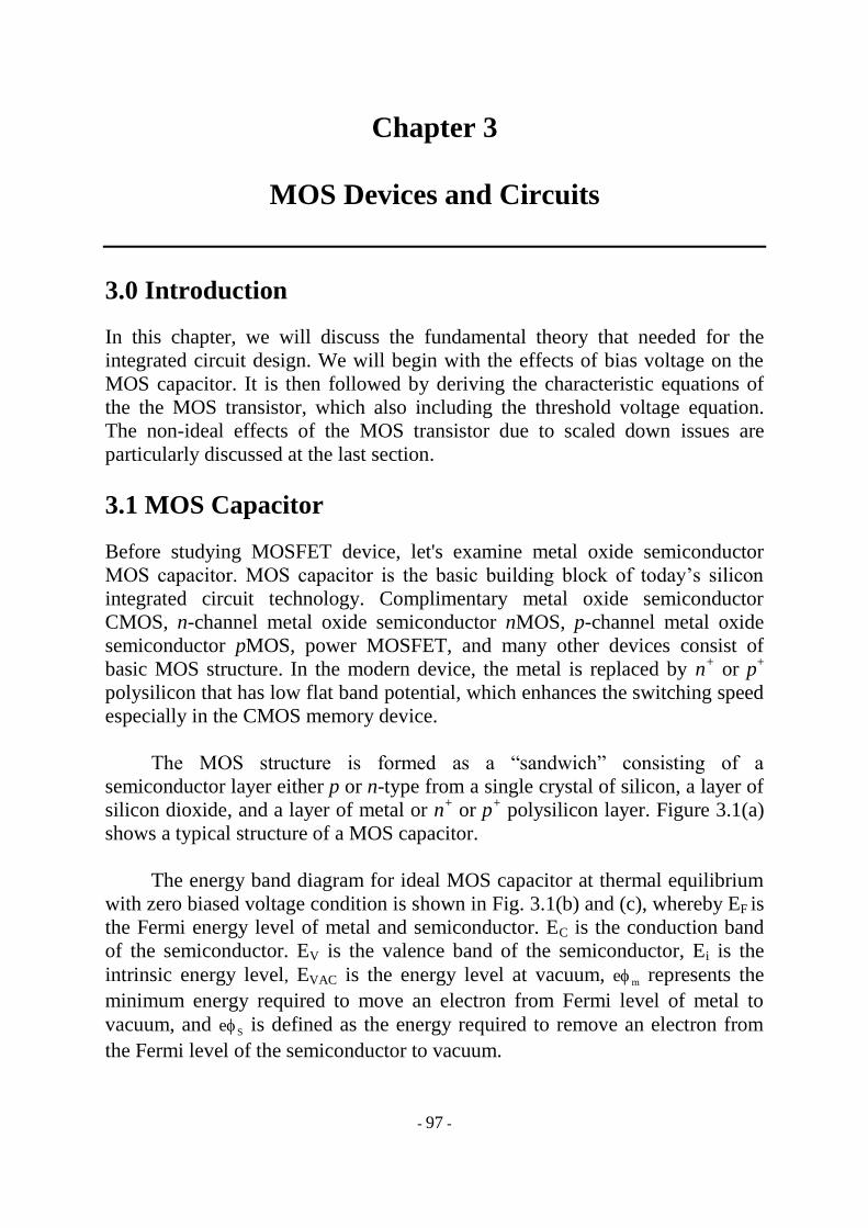
The MOS structure is formed as a “sandwich” consisting of a
semiconductor layer either p or n-type from a single crystal of silicon, a layer of
silicon dioxide, and a layer of metal or n+ or p
+ polysilicon layer. Figure 3.1(a)
shows a typical structure of a MOS capacitor.
The energy band diagram for ideal MOS capacitor at thermal equilibrium
with zero biased voltage condition is shown in Fig. 3.1(b) and (c), whereby EF is
the Fermi energy level of metal and semiconductor. EC is the conduction band
of the semiconductor. EV is the valence band of the semiconductor, Ei is the
intrinsic energy level, EVAC is the energy level at vacuum, e m represents the
minimum energy required to move an electron from Fermi level of metal to
vacuum, and e S is defined as the energy required to remove an electron from
the Fermi level of the semiconductor to vacuum.
3 MOS Devices and Circuits
- 98 -
(a)
`
(b)
(c)
Figure 3.1: A 2-D schematic structure of a MOS device Energy band diagram of the MOS
structure at thermal equilibrium with zero bias voltage condition
3 MOS Devices and Circuits
- 99 -
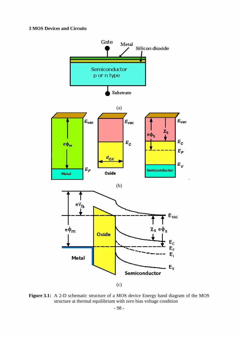
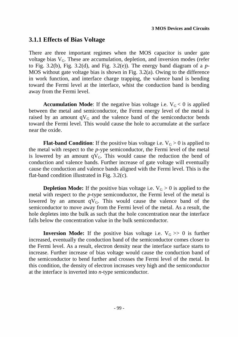
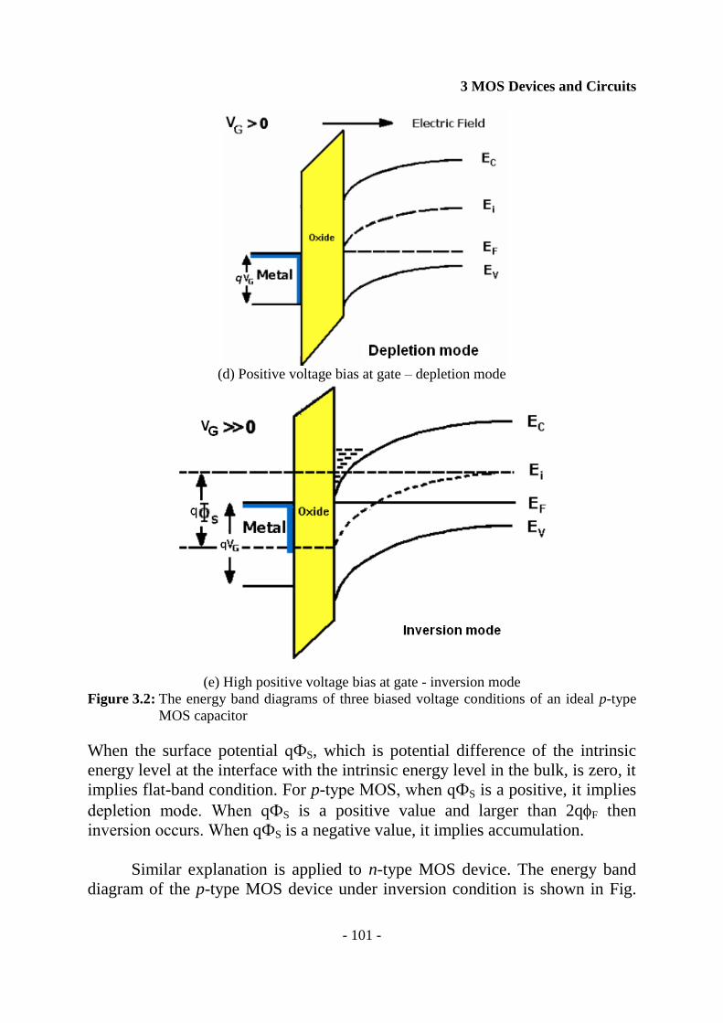
3.1.1 Effects of Bias Voltage
There are three important regimes when the MOS capacitor is under gate
voltage bias VG. These are accumulation, depletion, and inversion modes (refer
to Fig. 3.2(b), Fig. 3.2(d), and Fig. 3.2(e)). The energy band diagram of a p-
MOS without gate voltage bias is shown in Fig. 3.2(a). Owing to the difference
in work function, and interface charge trapping, the valence band is bending
toward the Fermi level at the interface, whist the conduction band is bending
away from the Fermi level.
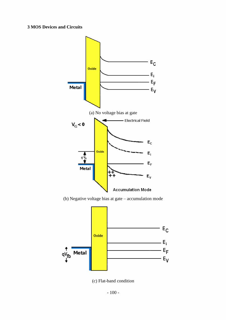
Accumulation Mode: If the negative bias voltage i.e. VG < 0 is applied
between the metal and semiconductor, the Fermi energy level of the metal is
raised by an amount qVG and the valence band of the semiconductor bends
toward the Fermi level. This would cause the hole to accumulate at the surface
near the oxide.
Flat-band Condition: If the positive bias voltage i.e. VG > 0 is applied to
the metal with respect to the p-ype semiconductor, the Fermi level of the metal
is lowered by an amount qVG. This would cause the reduction the bend of
conduction and valence bands. Further increase of gate voltage will eventually
cause the conduction and valence bands aligned with the Fermi level. This is the
flat-band condition illustrated in Fig. 3.2(c).
Depletion Mode: If the positive bias voltage i.e. VG > 0 is applied to the
metal with respect to the p-type semiconductor, the Fermi level of the metal is
lowered by an amount qVG. This would cause the valence band of the
semiconductor to move away from the Fermi level of the metal. As a result, the
hole depletes into the bulk as such that the hole concentration near the interface
falls below the concentration value in the bulk semiconductor.
Inversion Mode: If the positive bias voltage i.e. VG >> 0 is further
increased, eventually the conduction band of the semiconductor comes closer to
the Fermi level. As a result, electron density near the interface surface starts to
increase. Further increase of bias voltage would cause the conduction band of
the semiconductor to bend further and crosses the Fermi level of the metal. In
this condition, the density of electron increases very high and the semiconductor
at the interface is inverted into n-type semiconductor.
3 MOS Devices and Circuits
- 100 -
(a) No voltage bias at gate
(b) Negative voltage bias at gate – accumulation mode
(c) Flat-band condition
3 MOS Devices and Circuits
- 101 -
(d) Positive voltage bias at gate – depletion mode
(e) High positive voltage bias at gate - inversion mode
Figure 3.2: The energy band diagrams of three biased voltage conditions of an ideal p-type
MOS capacitor
When the surface potential qФS, which is potential difference of the intrinsic
energy level at the interface with the intrinsic energy level in the bulk, is zero, it
implies flat-band condition. For p-type MOS, when qФS is a positive, it implies
depletion mode. When qФS is a positive value and larger than 2qF then
inversion occurs. When qФS is a negative value, it implies accumulation.
Similar explanation is applied to n-type MOS device. The energy band
diagram of the p-type MOS device under inversion condition is shown in Fig.
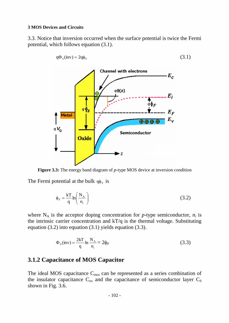
3 MOS Devices and Circuits
- 102 -
3.3. Notice that inversion occurred when the surface potential is twice the Fermi
potential, which follows equation (3.1).
FS q2)inv(q (3.1)
Figure 3.3: The energy band diagram of p-type MOS device at inversion condition
The Fermi potential at the bulk Fq is
i
AF
Nln
q
kT
n (3.2)
where NA is the acceptor doping concentration for p-type semiconductor, ni is
the intrinsic carrier concentration and kT/q is the thermal voltage. Substituting
equation (3.2) into equation (3.1) yields equation (3.3).
i
AS
Nln
q
kT2)inv(
n = 2F (3.3)
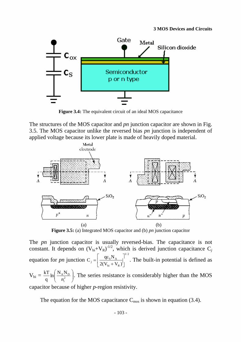
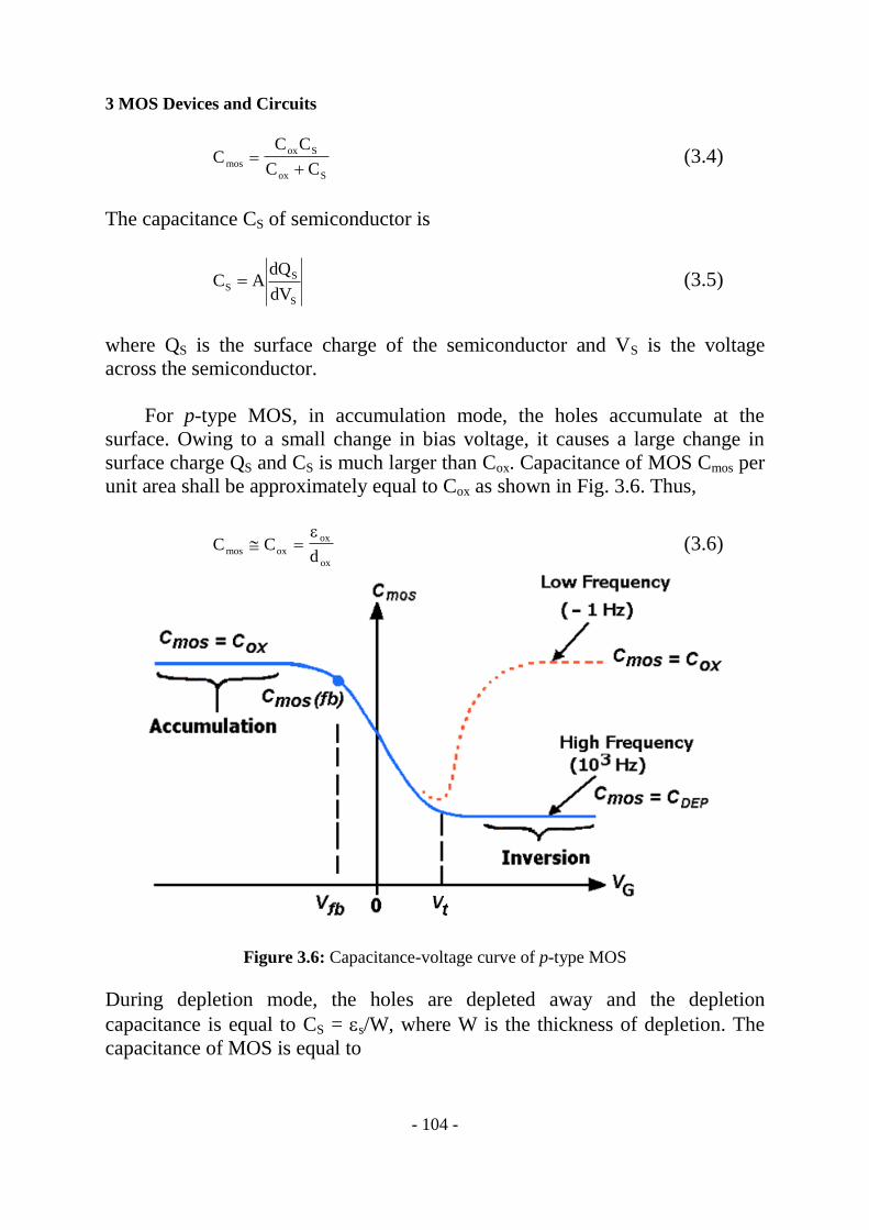
3.1.2 Capacitance of MOS Capacitor
The ideal MOS capacitance Cmos can be represented as a series combination of
the insulator capacitance Cox and the capacitance of semiconductor layer CS
shown in Fig. 3.6.
3 MOS Devices and Circuits
- 103 -
Figure 3.4: The equivalent circuit of an ideal MOS capacitance
The structures of the MOS capacitor and pn junction capacitor are shown in Fig.
3.5. The MOS capacitor unlike the reversed bias pn junction is independent of
applied voltage because its lower plate is made of heavily doped material.
(a) (b)
Figure 3.5: (a) Integrated MOS capacitor and (b) pn junction capacitor
The pn junction capacitor is usually reversed-bias. The capacitance is not
constant. It depends on (Vbi+VR)-1/2
, which is derived junction capacitance Cj
equation for pn junction
2/1
Rbi
AS
)VV(2
NqC
j . The built-in potential is defined as
Vbi =
2
i
DANNln
q
kT
n. The series resistance is considerably higher than the MOS
capacitor because of higher p-region resistivity.
The equation for the MOS capacitance Cmos is shown in equation (3.4).
3 MOS Devices and Circuits
- 104 -
CC C
C Cmos
ox S
ox S
(3.4)
The capacitance CS of semiconductor is
C AdQ
dVS
S
S
(3.5)
where QS is the surface charge of the semiconductor and VS is the voltage
across the semiconductor.
For p-type MOS, in accumulation mode, the holes accumulate at the
surface. Owing to a small change in bias voltage, it causes a large change in
surface charge QS and CS is much larger than Cox. Capacitance of MOS Cmos per
unit area shall be approximately equal to Cox as shown in Fig. 3.6. Thus,
C Cdmos ox
ox
ox
(3.6)
Figure 3.6: Capacitance-voltage curve of p-type MOS
During depletion mode, the holes are depleted away and the depletion
capacitance is equal to CS = s/W, where W is the thickness of depletion. The
capacitance of MOS is equal to
3 MOS Devices and Circuits
- 105 -
CC
C
Cd
Wmos
ox
ox
S
ox
ox
ox
S
1
(3.7)
At inversion, the depletion width reaches its maximum value Wmax. At this point
essential there is no free density. Thus, the capacitance Cmos reaches its
minimum value.
CC
C
Cd
Wmos
ox
ox
S
ox
ox
ox
S
(min)max
1
(3.8)
Thus, Cs << Cox and as the consequence, the capacitor of MOS is approaching
the value of Cs.
At flat-band position, the capacitance of semiconductor CSfb per unit area at
flat-band is
A
S
SS
qNq
kTC
fb (3.9)
Substituting equation (3.9) into equation (3.7) and using Cox = ox oxd/ , the
capacitance of MOS at flat-band Cmos(fb) is
A
s
s
oxox
oxmos
qN
q/kTd
)(C
fb (3.10)
So far what has been discussed is applicable to the ideal MOS capacitor. For the
non-ideal MOS capacitor, when the MOS capacitor is in inversion and depletion
modes, the capacitance of semiconductor CS has two major components. One is
the capacitance due to depletion CDEP and the other is due to inversion caused
by accumulation of minority carrier CMC. Therefore, the capacitance of
semiconductor CS shall have the relationship as specified in equation (3.11).
CS = CDEP + CMC (3.11)
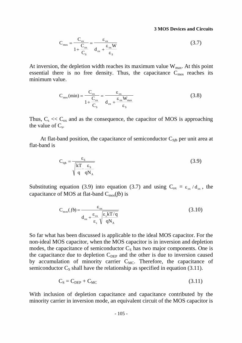
With inclusion of depletion capacitance and capacitance contributed by the
minority carrier in inversion mode, an equivalent circuit of the MOS capacitor is
3 MOS Devices and Circuits
- 106 -
shown in Fig. 3.7, whereby RS is the resistance of semiconductor bulk layer and
RGEN is the differential resistance which can be estimated as
Rd
dIGEN
S
GEN
(3.12)
where the s is the surface potential and generation current IGEN is
approximately proportional to the volume of depletion region, which follows
equation (3.13).
GEN
DEPiGEN
AdqnI
(3.13)
where GEN is an effective generation time constant.
Figure 3.7: The equivalent circuit of the MOS capacitor
Substituting equation (3.11) into equation (3.4), the MOS capacitance Cmos
becomes
CC C C
C C Cmos
ox DEP MC
ox DEP MC
( ) (3.14)
In the high frequency ( 2 f) mode whereby , the capacitance due to
minority carrier will approach zero. Hence, the MOS capacitance Cmos will
become
CC C
C Cmos
ox DEP
ox DEP
(3.15)
3 MOS Devices and Circuits
- 107 -
Likewise for low frequency mode whereby 0 , the capacitance due to
depletion is at minimum and the minority capacitance will approach the static
capacitance of bulk semiconductor CS. Thus, the MOS capacitance Cmos will
follow equation (3.6).
In strong inversion CMC >> Cox, the MOS capacitance will approach the
capacitance of insulator Cox. One also can say that the magnitude of the
capacitances are such that CMC > Cox > CDEP at strong inversion.
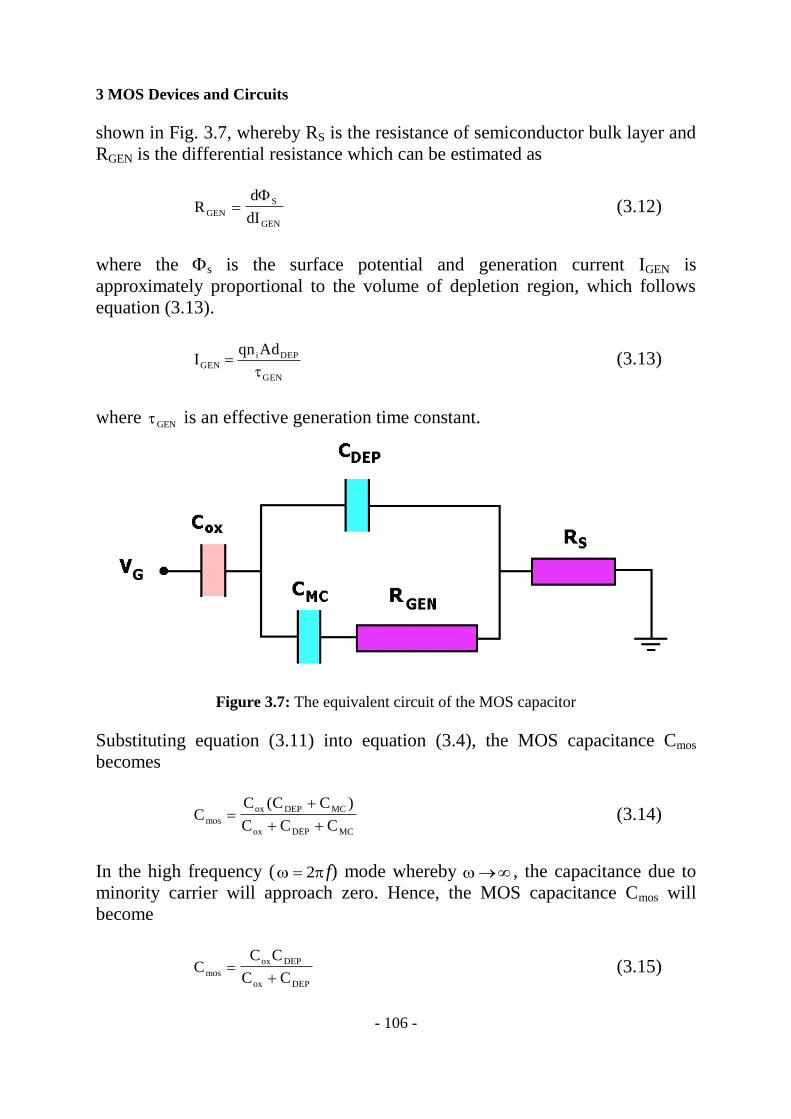
The change of threshold voltage as the result of fixed charge density NT is
equal to ox
oxTt
dqNV
. This shall mean that presence of positive fixed charge
would shift the capacitance-voltage curve toward more negative region as
shown in Fig. 3.8.
Figure 3.8: CV plot for the presence of fixed charge
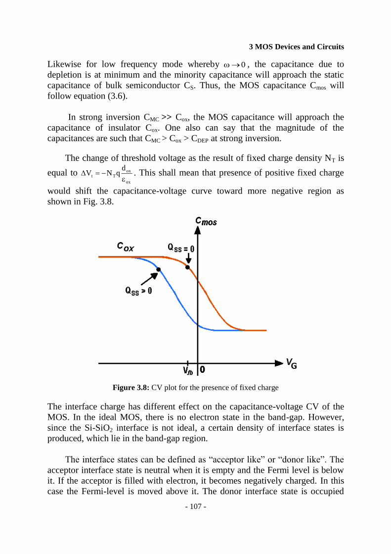
The interface charge has different effect on the capacitance-voltage CV of the
MOS. In the ideal MOS, there is no electron state in the band-gap. However,
since the Si-SiO2 interface is not ideal, a certain density of interface states is
produced, which lie in the band-gap region.
The interface states can be defined as “acceptor like” or “donor like”. The
acceptor interface state is neutral when it is empty and the Fermi level is below
it. If the acceptor is filled with electron, it becomes negatively charged. In this
case the Fermi-level is moved above it. The donor interface state is occupied
3 MOS Devices and Circuits
- 108 -
with electron and it is below Fermi level. It becomes positively charge if it is
empty and the Fermi level will move below it. Thus, Fermi level is altered by
the presence of charge in the interface state.
When the interface charge is positive, the CV curve shifts toward negative
voltage region. When it is negative, the curve shifts toward positive voltage
region. The result is shown in Fig. 3.9. If the interface density is maintained
below 1010
cm-2
, the effect of interface state on CV curve is negligible.
Figure 3.9: The effect of interface state on CV plot of a MOS
3.1.3 Threshold Voltage of MOS Capacitor
Threshold voltage Vt is defined as the gate voltage VG needed to induce
sufficient number of charge carrier in the channel for conduction. It is the
minimum applied gate voltage to induce inversion of the channel for
conduction. To find the threshold voltage Vt, one needs to understand how the
voltage is dropped across the MOS capacitor.
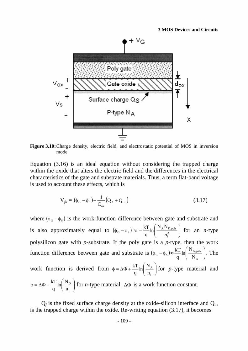
Fig. 3.10 shows the MOS structure with a voltage VG applied to its gate.
Applying Kirchhoff‟s voltage law, the gate voltage VG is
VG = Vox + Vs (3.16)
3 MOS Devices and Circuits
- 109 -
Figure 3.10: Charge density, electric field, and electrostatic potential of MOS in inversion
mode
Equation (3.16) is an ideal equation without considering the trapped charge
within the oxide that alters the electric field and the differences in the electrical
characteristics of the gate and substrate materials. Thus, a term flat-band voltage
is used to account these effects, which is
Vfb = ox
ox
SG QQC
1 f (3.17)
where SG is the work function difference between gate and substrate and
is also approximately equal to SG
2
i
poly,DA NNln
q
kT
n for an n-type
polysilicon gate with p-substrate. If the poly gate is a p-type, then the work
function difference between gate and substrate is SG
A
poly,A
N
Nln
q
kT. The
work function is derived from
i
A
n
Nln
q
kTfor p-type material and
i
D
n
Nln
q
kT for n-type material. is a work function constant.
Qf is the fixed surface charge density at the oxide-silicon interface and Qox
is the trapped charge within the oxide. Re-writing equation (3.17), it becomes
3 MOS Devices and Circuits
- 110 -
Vfb = ox
ox
2
i
poly,DA
C
n
NNln
q
kT
f (3.18)
Equation (3.16) shall then be modified to
VG = Vfb + Vox + VS (3.19)
The voltage drops across oxide Vox is Vox = Eox.dox. At semiconductor-oxide
interface, the surface charge QS is also equal to charge on oxide Qox, which is
εsEs = εoxEox. Qox is also equal to Qox = CoxVox = ox
oxox
d
V . Thus, Vox is equal to
Vox = ox
oxSS dE
. Re-writing equation (3.19), it becomes
VG = Vfb + VS + S S
ox
E
C (3.20)
For charge balancing, QS = Qox = Qdep, where depletion charge Qdep is equal to
Qdep = qNAddep. The depletion thickness ddep is equal to ddep =
2/1
A
SS
qN
V2
. At
inversion, VG = Vtn and VS = 2F, ddep becomes maximum value. Thus, the
maximum depletion charge Qdepmax is equal to 2/1
FASqN4 and surface electric
field ES is ES = S
FAS
S
maxdep Nq4Q
. Substituting expression 2/1
FASqN4 to
replace εSES in equation (3.21), the threshold voltage equation becomes
oxFASFtn C/qN42VV fb (3.21)
or
oxSFtn C/Q2VV fb (3.22)
If the substrate of the MOS transistor is biased with a voltage VSUB then the
threshold voltage Vtn is redefined as
oxSUBFASFtn C/)V2(qN22VV fb (3.23)
3 MOS Devices and Circuits
- 111 -
The equation shows that the threshold voltage increases with positive VSUB bias
since the surface potential is increased by a value VSUB.
Under normal processing conditions, the flat-band voltage is negative and
usually yields a negative threshold voltage. For CMOS switching circuits that
use a positive power rail, a positive threshold voltage is needed. This is
accomplished by performing a threshold adjustment ion implant with a dose
giving the number of implanted ion. This modifies the equation for the value of
the threshold voltage. Implanting acceptor ions into the substrate is equivalent
to introducing additional bulk charge at the surface; the implant thus induces a
positive shift. The equation to follow for the ion implant adjustment is
ox
IoxSUBFASFtn
C
qDC/V2qN22VV fb (3.24)
where DI is the dosage, the number implanted ion per unit area.
If there is no substrate voltage VSUB, in which sometime is called zero
body bias then equation (3.23) becomes oxFASFtno C/)2(qN22VV fb ,
where Vtno is the threshold voltage without the substrate voltage or body bias
voltage. The equation (3.23) can be re-written in terms of Vtno and substrate
voltage as
FSUBF
OX
AS
tnotn 2)V2(C
qN2VV
(3.25)
The term OX
AS
C
qN2 is denoted as gamma , which is called bulk threshold
parameter. Equation (3.25) clearly shows that as the VSUB voltage increases the
threshold voltage of the device increases. Rewriting equation (3.25), it becomes
FSUBFtot 2)V2(VV (3.26)
The positive sign is used to denote n-MOS transistor and negative sign for p-
MOS transistor.
In order to eliminate the effect of parasitic npn or pnp transistor of the n-
MOS transistor and p-MOS transistor, the substrate of the p-MOS transistor,
which is an n-type semiconductor, is usually biased with VDD voltage, whilst the
substrate of n-MOS transistor, which is p-type semiconductor, is biased with
VSS voltage i.e. zero volt.
3 MOS Devices and Circuits
- 112 -
By Kirchhoff‟s voltage law, the source voltage VS and substrate voltage
VSUB relationship is –VS+VS-SUB+VSUB = 0. Equation (3.26) therefore can be
written as one equation for p-MOS transistor and one for n-MOS transistor.
They are
FSUBSSFtpotp 2)VV2(VV (3.27)
FSUBSSFtnotn 2)VV2(VV (3.28)
With substrate of p-MOS transistor biased with VDD, and source and substrate
are tied together, the VSUB-S is equal to zero. Therefore, the threshold voltage of
p-MOS transistor is
FDDFtpotp 2)V2(VV (3.29)
With the substrate of n-MOS transistor biased with VSS and source and substrate
are tied together, VS-SUB is equal to zero. Therefore, the threshold voltage of the
n-MOS transistor is
tnoFFtnotn V2)2(VV (3.30)
One can see that Vtp of p-MOS transistor is lower than Vtpo, whilst the Vtn of n-
MOSFET is same as Vtno for the substrate biased condition mentioned above.
3.2 MOSFET
A MOSFET is a voltage control current device and is essentially consist of a
MOS capacitor and two diffused or implanted regions that serve as ohmic
contacts to an inversion layer of free charge carriers with the semiconductor-
silicon dioxide interface. The metal gate is essentially either p+ or n
+ polysilicon
type.
There are two types of MOSFET namely depletion-enhancement DE and
enhancement E types. Figure 3.11 and 3.12 show the difference between the
types.
The DE type has a narrow channel adjacent to the gate connecting the drain
and source of the transistor. It can operate in either depletion mode or
enhancement mode. The mode of operation is like the JFET.
3 MOS Devices and Circuits
- 113 -
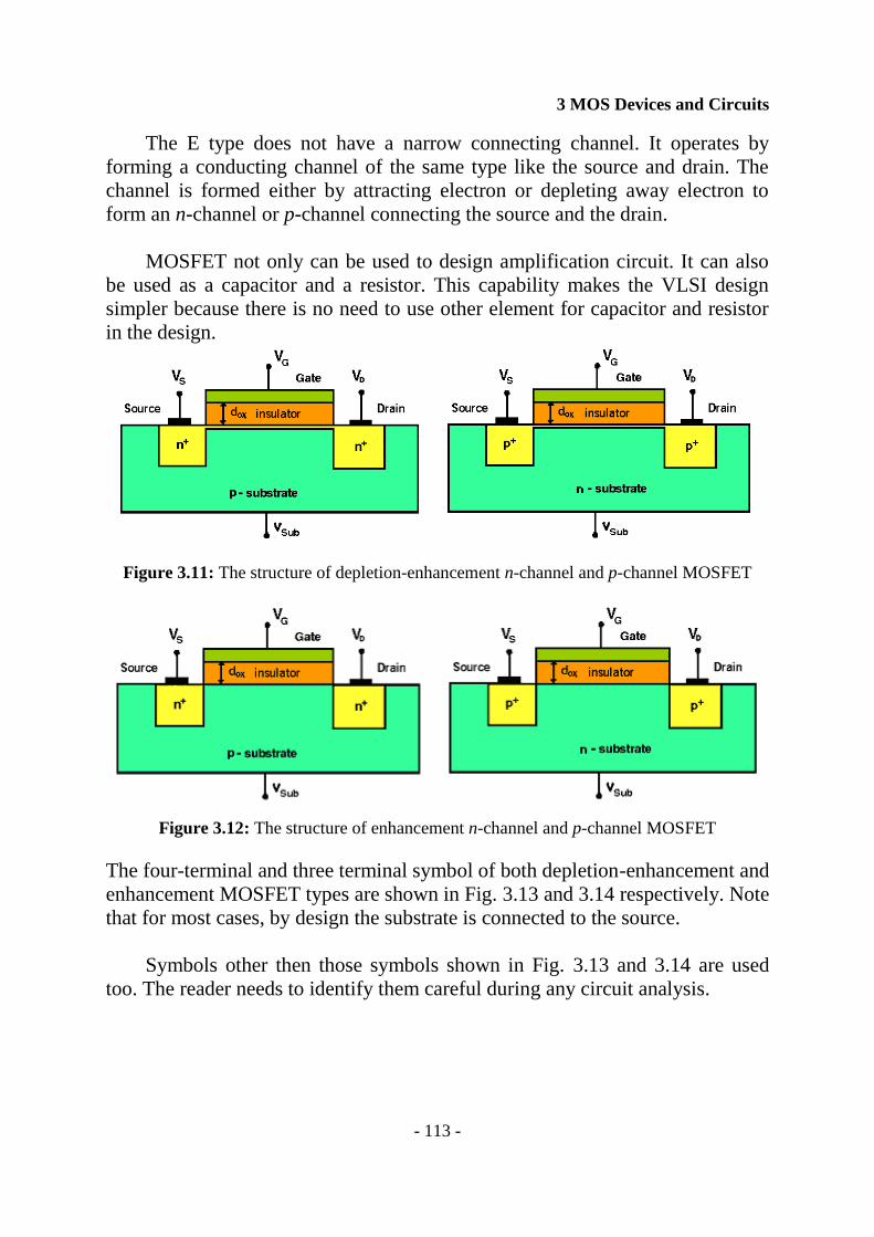
The E type does not have a narrow connecting channel. It operates by
forming a conducting channel of the same type like the source and drain. The
channel is formed either by attracting electron or depleting away electron to
form an n-channel or p-channel connecting the source and the drain.
MOSFET not only can be used to design amplification circuit. It can also
be used as a capacitor and a resistor. This capability makes the VLSI design
simpler because there is no need to use other element for capacitor and resistor
in the design.
Figure 3.11: The structure of depletion-enhancement n-channel and p-channel MOSFET
Figure 3.12: The structure of enhancement n-channel and p-channel MOSFET
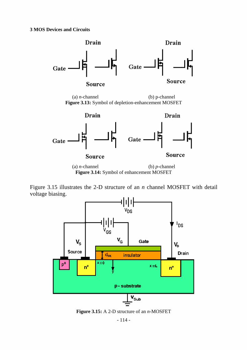
The four-terminal and three terminal symbol of both depletion-enhancement and
enhancement MOSFET types are shown in Fig. 3.13 and 3.14 respectively. Note
that for most cases, by design the substrate is connected to the source.
Symbols other then those symbols shown in Fig. 3.13 and 3.14 are used
too. The reader needs to identify them careful during any circuit analysis.
3 MOS Devices and Circuits
- 114 -
(a) n-channel (b) p-channel
Figure 3.13: Symbol of depletion-enhancement MOSFET
(a) n-channel (b) p-channel
Figure 3.14: Symbol of enhancement MOSFET
Figure 3.15 illustrates the 2-D structure of an n channel MOSFET with detail
voltage biasing.
Figure 3.15: A 2-D structure of an n-MOSFET
3 MOS Devices and Circuits
- 115 -
Gradual Channel Approximation Model and Constant Mobility Approximation
Model can be used to study the characteristics of MOSFET. The model is used
to study how the conduction channel of the MOSFET is changed by the
horizontal electric field generated by the drain to source voltage VDS and how
the conducting channel is modulated by the vertical electric field generated by
the gate to source voltage VGS. This is done by studying the drain to source
current IDS versus drain to source voltage VDS characteristic for different applied
gate to source voltage VGS and the transconductance of the device, which is the
study of IDS current changes with the change of VGS voltage. These two studies
are connected with the physical studies of the linear and saturation regions of
the drain to source characteristics with various gate-to-source voltage VGS.
Based on this understanding, one has to look at the two dimensional Poisson‟s
equation in order to understand the actual conduction mechanism of current
from drain to source via the inverted channel.
There are two electric field components present in MOSFET when it is in
operation. These fields can be represented by the two dimensional Poisson‟s
equation that has one horizontal field EX and one vertical field EY.
E
X
E
Y
X Y
S
(3.31)
Gradual Channel Approximation Model is true only if
E
X
X is very small and
constant so that the Poisson‟s equation can be approximated as
E
Y
Y
S
(3.32)
The vertical electric potential of the conduction channel with thickness d is
given as
E
Y
E
d
Y Y .
q/kTd
VV
Y
E2
ox
2
tGS
2
s
oxY
(3.33)
On the other hand, the variation of horizontal electric field can be approximated
as
3 MOS Devices and Circuits
- 116 -
E
X
V
L
X DS 2 (3.34)
where L is the channel length and VDS is the voltage between drain and source
of the MOS transistor. Here, it is assumed that the field strength changes
gradually from a small value near the source to a value of the order VDS/L near
the drain.
The mobilities of the electron and hole n, p of the MOS transistor are not
the same as the mobility in the semiconductor bulk moving into the crystal
lattice. Knowing the electrons or holes are moving on the surface between the
semiconductor and oxide interface, their mobilities are very much depending on
the surface impeding collision and ionized impurity scattering. However
electrons and holes moving not closed to the interface would have a higher
mobility. One also has to consider the influence of horizontal electric field
resulted from drain to source voltage. Thus, there is an effective mobility for
both hole and electron.
If the drain-to-source voltage is small, the effective channel length and
carrier charge will be more or less uniform from the source to drain and
effective mobility will be essentially the same for all x values. However, one
cannot ignore the effect of gate voltage on the mobility. As the gate-to-source
voltage increases, the electron is moving closed to the interface. The effect of
scattering will be more. Thus mobility decreases which can be observed from
equation (3.35).
)VV(1 tGS
0
n
(3.35)
where 0 is constant and is the mobility degradation parameter. It can be
shown that the effective mobility n of electron is about 0.6 of the bulk mobility
at (VGS – Vt) = 4V to about 0.5 for (VGS – Vt) = 13V.
3.2.1 Current-Voltage Characteristics
The surface potential above threshold regime is equal to Vs(x) = ( ( ))2F V x ,
where V(x) is the channel potential at position x along the channel in the
direction from source to drain. However, from Gradual Channel Approximation
Model, one can say that V(x) is equal to zero at the source side because the
source and the substrate are normally shorted together and biased at VSS for an
3 MOS Devices and Circuits
- 117 -
n-MOS transistor and biased at VDD for p-MOS transistor. Thus, V(x) is equal to
the drain-to-source voltage VDS at the drain side. This shall mean that the gate
voltage with respect to source VGS is equal to
)x(V2C
)x(QVV F
ox
s
GS fb (3.36)
Qs(x) is the surface charge, which is consisting of free electron charge Qn(x) and
fixed charge acceptors in the depletion region QDEP(x). Therefore, the surface
charge of is given by equation (3.38).
Qs(x) = Qn(x) + QDEP(x) (3.37)
From Constant Mobility Approximation Model, the electron mobility µn is
constant and there is only drift and negligible diffusion, the drain-to-source
current IDS can be calculated from current density Jn = qnnE after ignoring the
diffusion portion qDndx
dn. Indeed drift current is only required to be considered
since the drain is reversed biased with respect to source.
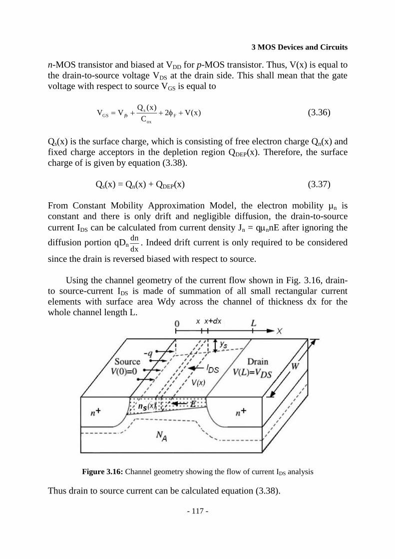
Using the channel geometry of the current flow shown in Fig. 3.16, drain-
to source-current IDS is made of summation of all small rectangular current
elements with surface area Wdy across the channel of thickness dx for the
whole channel length L.
Figure 3.16: Channel geometry showing the flow of current IDS analysis
Thus drain to source current can be calculated equation (3.38).
3 MOS Devices and Circuits
- 118 -
)x(y
0
nynyDS dyJWdydwJI
dy)y,x(n)y,x(q
dx
)x(dVW
)x(y
0
sn
(3.38)
where the second expression of equation (3.38) is equal to effective mobility of
the electron n , which is equation (3.35). Knowing that the threshold voltage is
Vt = 2F +Vfb +ox
DEP
C
Q and nsOXFGS V)x(V)x(VV2V fb after inversion with
mobile ion density ns, the surface free charge density per unit area ns(x) in x-
direction is
q
2)x(VN2)x(VV2V
q
C)x(n FAS
FGSox
S
fb (3.39)
Substituting equation (3.39) into IDSdx = qnnsWdV(x) and integrating the
equation with the boundary conditions for V x x( ) 0= 0 and V x x L( )
= VDS and x
= 0 to x = L, IDS, it yields the drain to source equation (3.34).
DS
DS
FGS
oxn
DS V2
V2VV
L
CWI
fb
2/3
F
2/3
FDS
ox
AS22V
C3
qN22 (3.40)
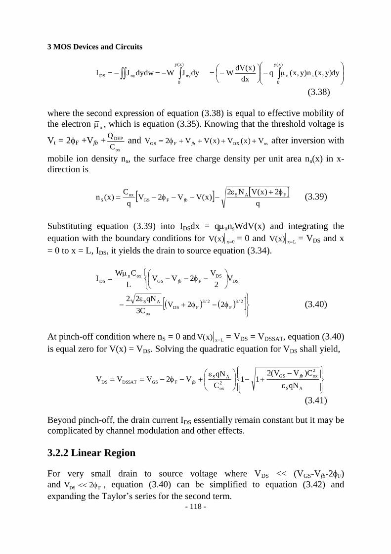
At pinch-off condition where nS = 0 and V x x L( ) = VDS = VDSSAT, equation (3.40)
is equal zero for V(x) = VDS. Solving the quadratic equation for VDS shall yield,
2
ox
AS
FGSDSSATDSC
qNV2VVV fb
AS
2
oxGS
qN
C)VV(211
fb
(3.41)
Beyond pinch-off, the drain current IDS essentially remain constant but it may be
complicated by channel modulation and other effects.
3.2.2 Linear Region
For very small drain to source voltage where VDS << (VGS-Vfb-2F)
and VDS F 2 , equation (3.40) can be simplified to equation (3.42) and
expanding the Taylor‟s series for the second term.
3 MOS Devices and Circuits
- 119 -
2
VV)VV(
L
CWI
2
DS
DStGS
oxn
DS (3.42)
This is the equation for the linear region of the MOSFET‟s characteristics.
3.2.3 Saturation Region
After pinch-off, IDS is assumed to be constant. It is true only if the doping
concentration is low and the oxide thickness is thin. The term in equation (3.41)
involving N CA ox/ 2 can be ignored and terms involving N CA ox/ can be
retained. This gives the shall mean that
VDSSAT = 2/1
GS
ox
AS
FGS VVC
qN22VV fbfb
(3.43)
If the voltage drops across the oxide is negligible, then at strong inversion the
quantity (VGS – Vfb) is equal to VGS – Vfb 2F. Based on the above assumption,
equation (3.43) can be simplified as
VDSSAT = tGS VV (3.44)
After substituting equation (3.43) into equation (3.43),
2
)VV()VV(2VV
L
CWI
2
tGS
tGFGS
oxn
DSSAT
fb
2/3
F
2/3
FtGS
ox
AS22VV
C3
qN22 (3.45)
Since the current does not change with VDS in this equation, further
simplification can be done once pinch-off occurred. i.e. N CA ox/ is small such
that Vt Vfb + 2F. The equation (3.45) shall be simplified to
2
)VV(VV
L
CWI
2
tGS2
tGS
oxn
DSSAT (3.46)
= 2
tGS
oxn )VV(L2
CW
This is the equation for the saturation region of the MOS transistor
characteristics.
3 MOS Devices and Circuits
- 120 -
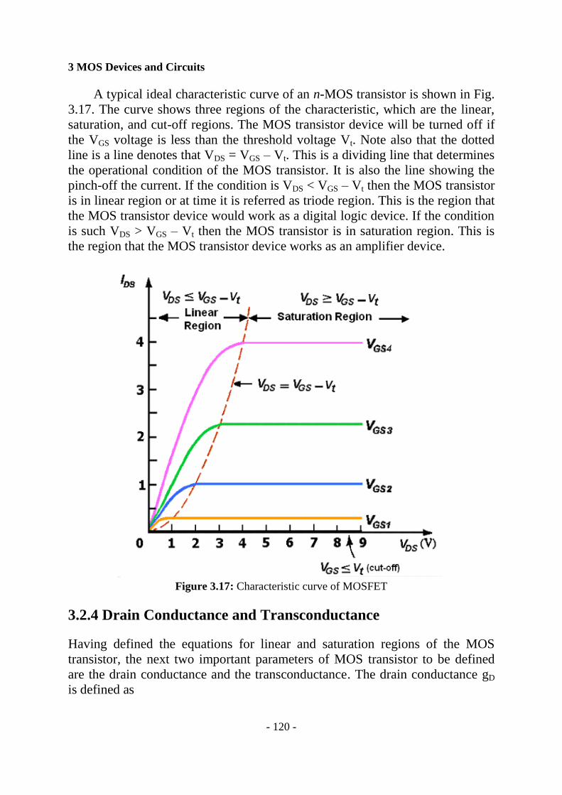
A typical ideal characteristic curve of an n-MOS transistor is shown in Fig.
3.17. The curve shows three regions of the characteristic, which are the linear,
saturation, and cut-off regions. The MOS transistor device will be turned off if
the VGS voltage is less than the threshold voltage Vt. Note also that the dotted
line is a line denotes that VDS = VGS – Vt. This is a dividing line that determines
the operational condition of the MOS transistor. It is also the line showing the
pinch-off the current. If the condition is VDS < VGS – Vt then the MOS transistor
is in linear region or at time it is referred as triode region. This is the region that
the MOS transistor device would work as a digital logic device. If the condition
is such VDS > VGS – Vt then the MOS transistor is in saturation region. This is
the region that the MOS transistor device works as an amplifier device.
Figure 3.17: Characteristic curve of MOSFET
3.2.4 Drain Conductance and Transconductance
Having defined the equations for linear and saturation regions of the MOS
transistor, the next two important parameters of MOS transistor to be defined
are the drain conductance and the transconductance. The drain conductance gD
is defined as
3 MOS Devices and Circuits
- 121 -
gI
VD
DS
DS V Cons tGS
tan
)VV(L
CWtGS
oxn
(3.47)
Drain conductance is also equal to equation (3.42) if the term VDS is moved to
the left-hand side of the equation as denominator.
The transconductance gm at saturation region is defined as
)VV(L
CW
V
Ig tGS
oxn
ttanconsVGS
DSATT
m
DS
(3.48)
3.2.5 Cut-off Frequency
The cut-off frequency fmax of the MOS transistor is defined as the maximum
operating frequency of the MOS transistor when it is in saturation mode with
the assumption that the mobility of the carrier is constant. Thus, the cut-off
frequency for p-MOS transistor is defined as
fmax g
C
m
GS2 (3.49)
where CGS is the gate to source capacitance, which estimated to be oxide
capacitance per unit area multiplies by area WL. Thus, the gate to source
capacitance is WLCC oxGS .
fmax 2
tGSp
GS
m
L2
)VV(
C2
g
(3.50)
For the short channel device, the cut-off frequency is assumed to depend on the
transit time ttr of the carrier in the channel. Thus,
fmax 1
2t tr
(3.51)
where by ttr is also approximately equal to the channel length L divided by
carrier saturation velocity s . i.e. trr = L/Vs.
3 MOS Devices and Circuits
- 122 -
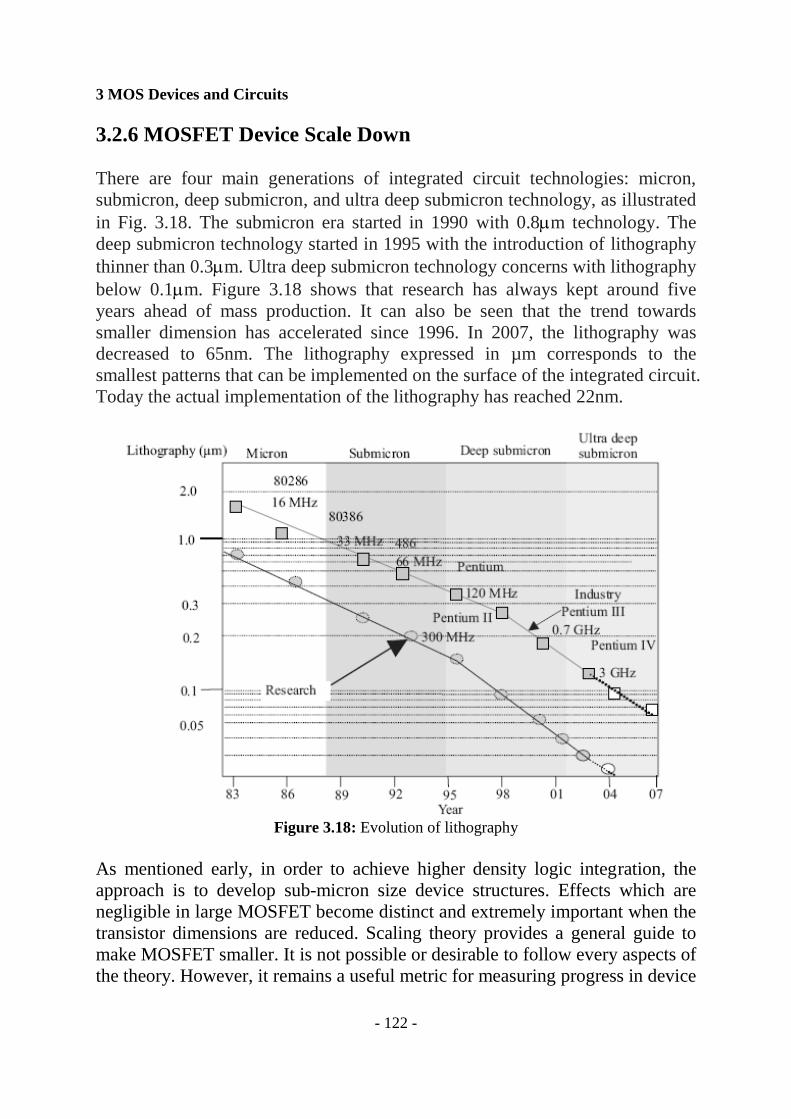
3.2.6 MOSFET Device Scale Down
There are four main generations of integrated circuit technologies: micron,
submicron, deep submicron, and ultra deep submicron technology, as illustrated
in Fig. 3.18. The submicron era started in 1990 with 0.8m technology. The
deep submicron technology started in 1995 with the introduction of lithography
thinner than 0.3m. Ultra deep submicron technology concerns with lithography
below 0.1m. Figure 3.18 shows that research has always kept around five
years ahead of mass production. It can also be seen that the trend towards
smaller dimension has accelerated since 1996. In 2007, the lithography was
decreased to 65nm. The lithography expressed in µm corresponds to the
smallest patterns that can be implemented on the surface of the integrated circuit.
Today the actual implementation of the lithography has reached 22nm.
Figure 3.18: Evolution of lithography
As mentioned early, in order to achieve higher density logic integration, the
approach is to develop sub-micron size device structures. Effects which are
negligible in large MOSFET become distinct and extremely important when the
transistor dimensions are reduced. Scaling theory provides a general guide to
make MOSFET smaller. It is not possible or desirable to follow every aspects of
the theory. However, it remains a useful metric for measuring progress in device
3 MOS Devices and Circuits
- 123 -
physics especially the simulation or prediction of the behavior of the device
with smaller dimension.
Scaling theory deals with the question of how the device characteristics are
changed as the dimensions of the device are reduced in an idealized well-
defined manner. Scaling theory is ideal ignoring many small-device effects that
govern the performance of MOSFET. It is often desirable to adhere to the large
device models for simplicity but modify the parameters to account for the more
important changes in the transistor parameters. Scaling of the device to smaller
dimension affects parameters such as threshold voltage and mobility. Smaller
channel length decreases the threshold voltage. Narrower device increases
threshold voltage. Small channel length increases horizontal electric field that
causes the MOSFET to operate with saturation velocity. This reduces the drain
current of the device. High electric field means high energetic carrier that can
enter the oxide to become trapped charge and affects the threshold voltage of
the MOS transistor.
The drain and source of the MOSFET are usually much heavily doped than
the bulk. Couple with high electric field, hot ion tunneling is unavoidable. This
issue causes leakage. In order to resolve this problem, lightly doped drain LDD
approach is adopted for the design of small dimension MOS transistor.
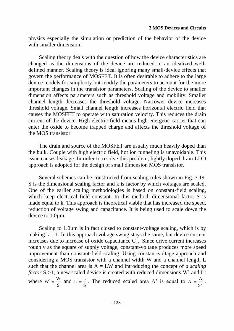
Several schemes can be constructed from scaling rules shown in Fig. 3.19.
S is the dimensional scaling factor and k is factor by which voltages are scaled.
One of the earlier scaling methodologies is based on constant-field scaling,
which keep electrical field constant. In this method, dimensional factor S is
made equal to k. This approach is theoretical viable that has increased the speed,
reduction of voltage swing and capacitance. It is being used to scale down the
device to 1.0µm.
Scaling to 1.0µm is in fact closed to constant-voltage scaling, which is by
making k = 1. In this approach voltage swing stays the same, but device current
increases due to increase of oxide capacitance Cox. Since drive current increases
roughly as the square of supply voltage, constant-voltage produces more speed
improvement than constant-field scaling. Using constant-voltage approach and
considering a MOS transistor with a channel width W and a channel length L
such that the channel area is A = LW and introducing the concept of a scaling
factor S >1, a new scaled device is created with reduced dimensions W‟ and L‟
where S
WW ' and
S
LL' . The reduced scaled area A‟ is equal to
2
'
S
AA .
3 MOS Devices and Circuits
- 124 -
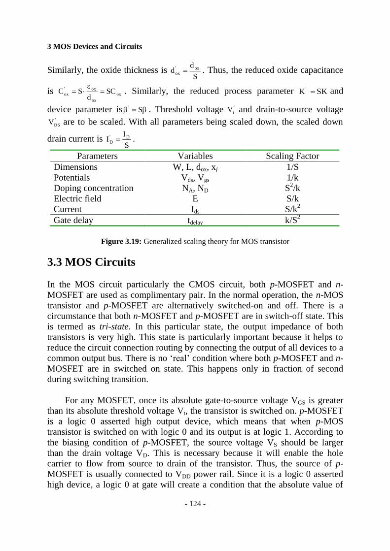
Similarly, the oxide thickness is S
dd ox'
ox . Thus, the reduced oxide capacitance
is ox
ox
ox'
ox SCd
SC . Similarly, the reduced process parameter SKK ' and
device parameter is S' . Threshold voltage '
tV and drain-to-source voltage '
DSV are to be scaled. With all parameters being scaled down, the scaled down
drain current is S
II D'
D .
Parameters Variables Scaling Factor
Dimensions W, L, dox, xj 1/S
Potentials Vds, Vgs 1/k
Doping concentration NA, ND S2/k
Electric field E S/k
Current Ids S/k2
Gate delay tdelay k/S2
Figure 3.19: Generalized scaling theory for MOS transistor
3.3 MOS Circuits
In the MOS circuit particularly the CMOS circuit, both p-MOSFET and n-
MOSFET are used as complimentary pair. In the normal operation, the n-MOS
transistor and p-MOSFET are alternatively switched-on and off. There is a
circumstance that both n-MOSFET and p-MOSFET are in switch-off state. This
is termed as tri-state. In this particular state, the output impedance of both
transistors is very high. This state is particularly important because it helps to
reduce the circuit connection routing by connecting the output of all devices to a
common output bus. There is no „real‟ condition where both p-MOSFET and n-
MOSFET are in switched on state. This happens only in fraction of second
during switching transition.
For any MOSFET, once its absolute gate-to-source voltage VGS is greater
than its absolute threshold voltage Vt, the transistor is switched on. p-MOSFET
is a logic 0 asserted high output device, which means that when p-MOS
transistor is switched on with logic 0 and its output is at logic 1. According to
the biasing condition of p-MOSFET, the source voltage VS should be larger
than the drain voltage VD. This is necessary because it will enable the hole
carrier to flow from source to drain of the transistor. Thus, the source of p-
MOSFET is usually connected to VDD power rail. Since it is a logic 0 asserted
high device, a logic 0 at gate will create a condition that the absolute value of
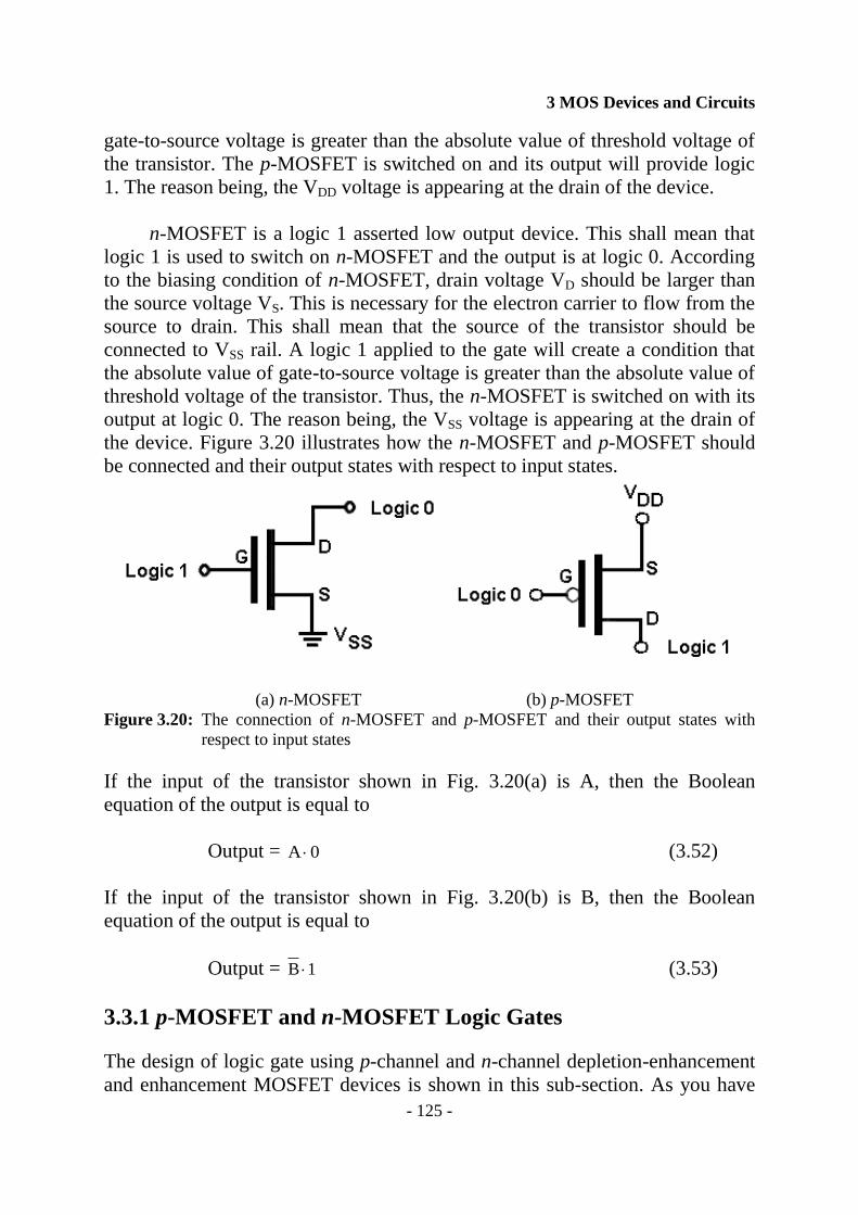
3 MOS Devices and Circuits
- 125 -
gate-to-source voltage is greater than the absolute value of threshold voltage of
the transistor. The p-MOSFET is switched on and its output will provide logic
1. The reason being, the VDD voltage is appearing at the drain of the device.
n-MOSFET is a logic 1 asserted low output device. This shall mean that
logic 1 is used to switch on n-MOSFET and the output is at logic 0. According
to the biasing condition of n-MOSFET, drain voltage VD should be larger than
the source voltage VS. This is necessary for the electron carrier to flow from the
source to drain. This shall mean that the source of the transistor should be
connected to VSS rail. A logic 1 applied to the gate will create a condition that
the absolute value of gate-to-source voltage is greater than the absolute value of
threshold voltage of the transistor. Thus, the n-MOSFET is switched on with its
output at logic 0. The reason being, the VSS voltage is appearing at the drain of
the device. Figure 3.20 illustrates how the n-MOSFET and p-MOSFET should
be connected and their output states with respect to input states.
(a) n-MOSFET (b) p-MOSFET
Figure 3.20: The connection of n-MOSFET and p-MOSFET and their output states with
respect to input states
If the input of the transistor shown in Fig. 3.20(a) is A, then the Boolean
equation of the output is equal to
Output = 0A (3.52)
If the input of the transistor shown in Fig. 3.20(b) is B, then the Boolean
equation of the output is equal to
Output = 1B (3.53)
3.3.1 p-MOSFET and n-MOSFET Logic Gates
The design of logic gate using p-channel and n-channel depletion-enhancement
and enhancement MOSFET devices is shown in this sub-section. As you have
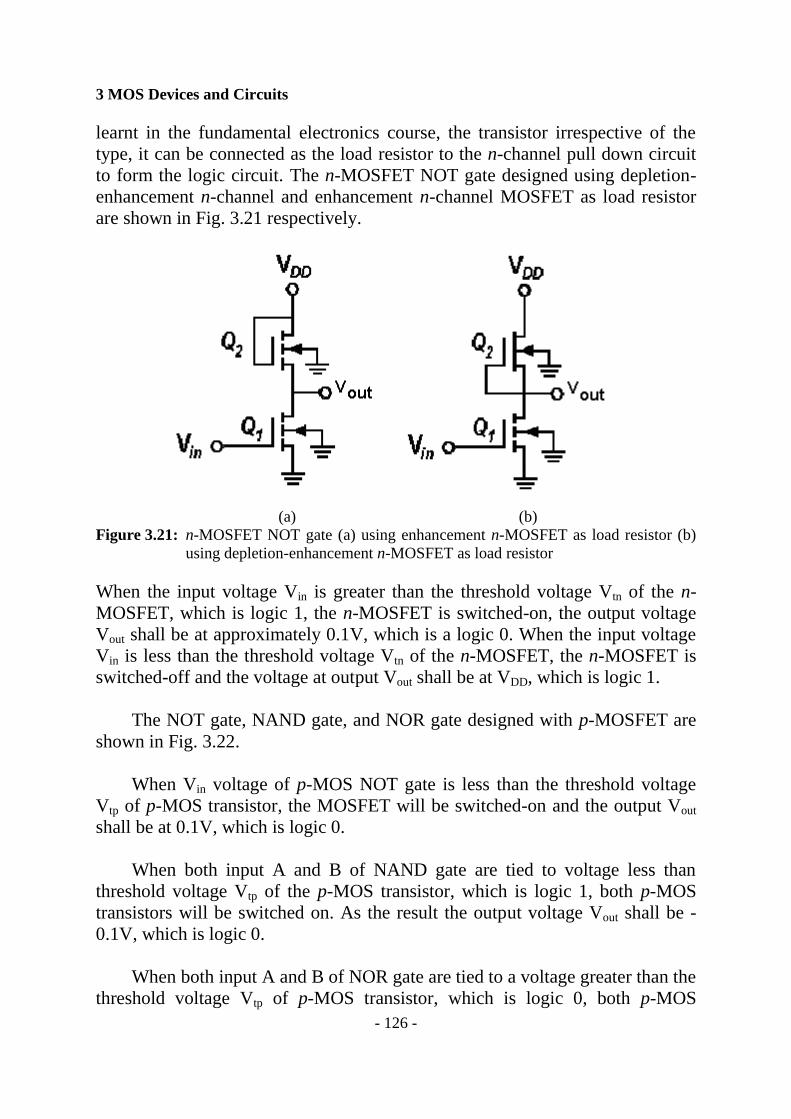
3 MOS Devices and Circuits
- 126 -
learnt in the fundamental electronics course, the transistor irrespective of the
type, it can be connected as the load resistor to the n-channel pull down circuit
to form the logic circuit. The n-MOSFET NOT gate designed using depletion-
enhancement n-channel and enhancement n-channel MOSFET as load resistor
are shown in Fig. 3.21 respectively.
(a) (b)
Figure 3.21: n-MOSFET NOT gate (a) using enhancement n-MOSFET as load resistor (b)
using depletion-enhancement n-MOSFET as load resistor
When the input voltage Vin is greater than the threshold voltage Vtn of the n-
MOSFET, which is logic 1, the n-MOSFET is switched-on, the output voltage
Vout shall be at approximately 0.1V, which is a logic 0. When the input voltage
Vin is less than the threshold voltage Vtn of the n-MOSFET, the n-MOSFET is
switched-off and the voltage at output Vout shall be at VDD, which is logic 1.
The NOT gate, NAND gate, and NOR gate designed with p-MOSFET are
shown in Fig. 3.22.
When Vin voltage of p-MOS NOT gate is less than the threshold voltage
Vtp of p-MOS transistor, the MOSFET will be switched-on and the output Vout
shall be at 0.1V, which is logic 0.
When both input A and B of NAND gate are tied to voltage less than
threshold voltage Vtp of the p-MOS transistor, which is logic 1, both p-MOS
transistors will be switched on. As the result the output voltage Vout shall be -
0.1V, which is logic 0.
When both input A and B of NOR gate are tied to a voltage greater than the
threshold voltage Vtp of p-MOS transistor, which is logic 0, both p-MOS
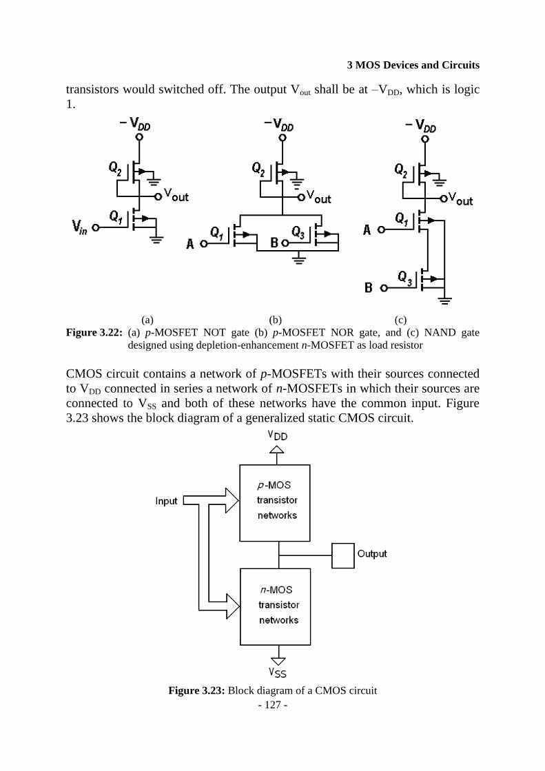
3 MOS Devices and Circuits
- 127 -
transistors would switched off. The output Vout shall be at –VDD, which is logic
1.
(a) (b) (c)
Figure 3.22: (a) p-MOSFET NOT gate (b) p-MOSFET NOR gate, and (c) NAND gate
designed using depletion-enhancement n-MOSFET as load resistor
CMOS circuit contains a network of p-MOSFETs with their sources connected
to VDD connected in series a network of n-MOSFETs in which their sources are
connected to VSS and both of these networks have the common input. Figure
3.23 shows the block diagram of a generalized static CMOS circuit.
Figure 3.23: Block diagram of a CMOS circuit
3 MOS Devices and Circuits
- 128 -
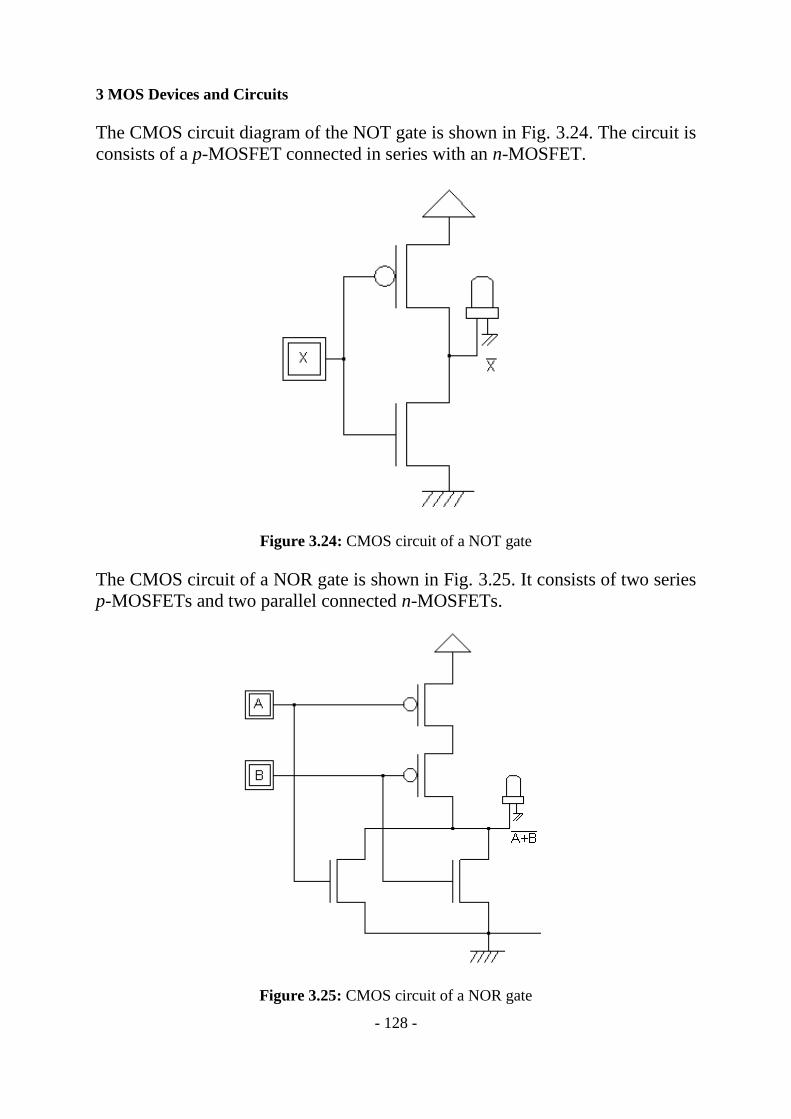
The CMOS circuit diagram of the NOT gate is shown in Fig. 3.24. The circuit is
consists of a p-MOSFET connected in series with an n-MOSFET.
Figure 3.24: CMOS circuit of a NOT gate
The CMOS circuit of a NOR gate is shown in Fig. 3.25. It consists of two series
p-MOSFETs and two parallel connected n-MOSFETs.
Figure 3.25: CMOS circuit of a NOR gate
3 MOS Devices and Circuits
- 129 -
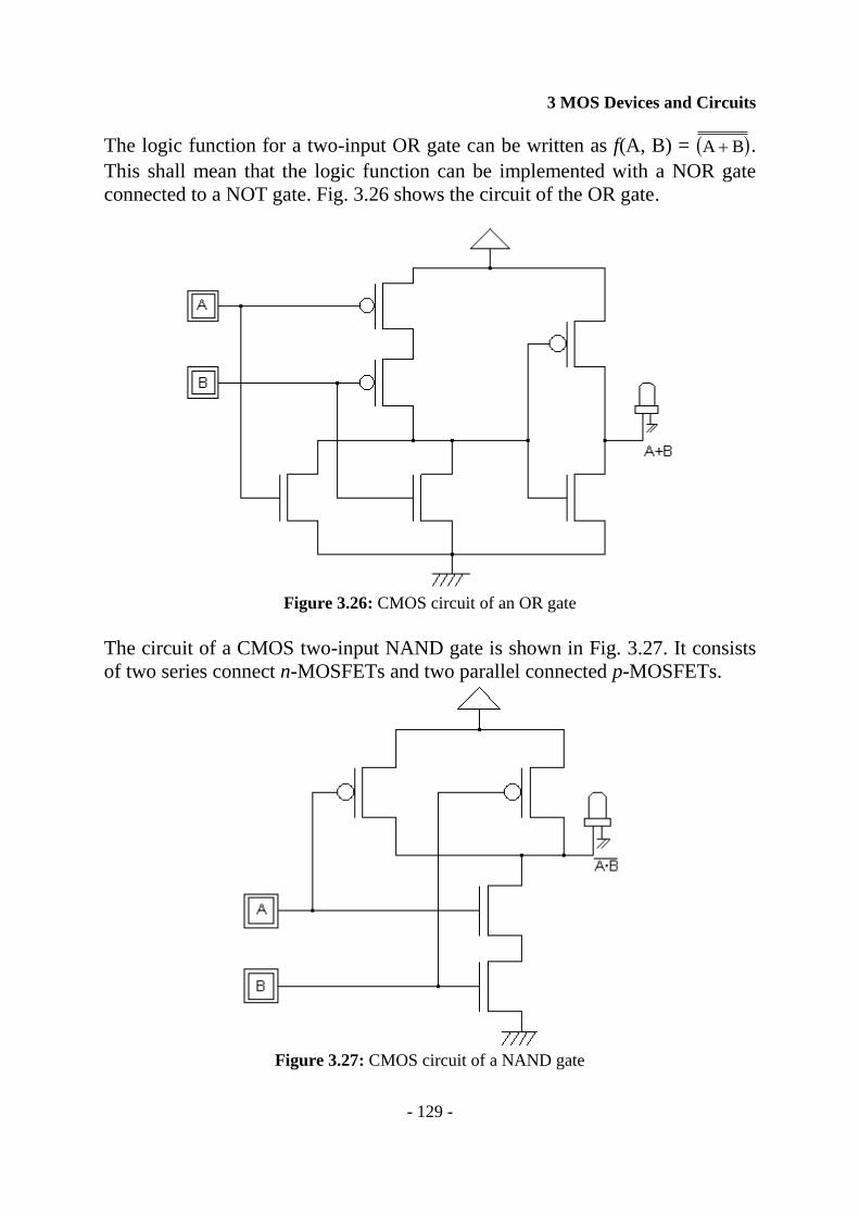
The logic function for a two-input OR gate can be written as f(A, B) = BA .
This shall mean that the logic function can be implemented with a NOR gate
connected to a NOT gate. Fig. 3.26 shows the circuit of the OR gate.
Figure 3.26: CMOS circuit of an OR gate
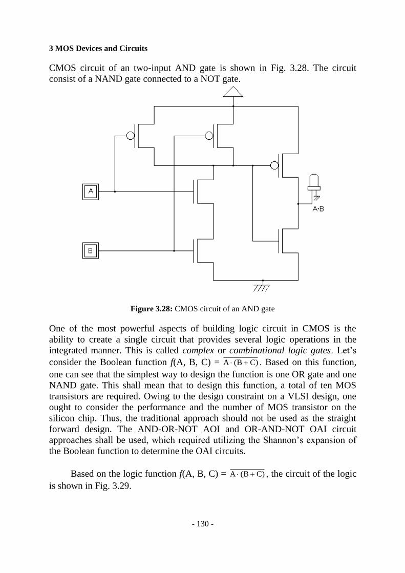
The circuit of a CMOS two-input NAND gate is shown in Fig. 3.27. It consists
of two series connect n-MOSFETs and two parallel connected p-MOSFETs.
Figure 3.27: CMOS circuit of a NAND gate
3 MOS Devices and Circuits
- 130 -
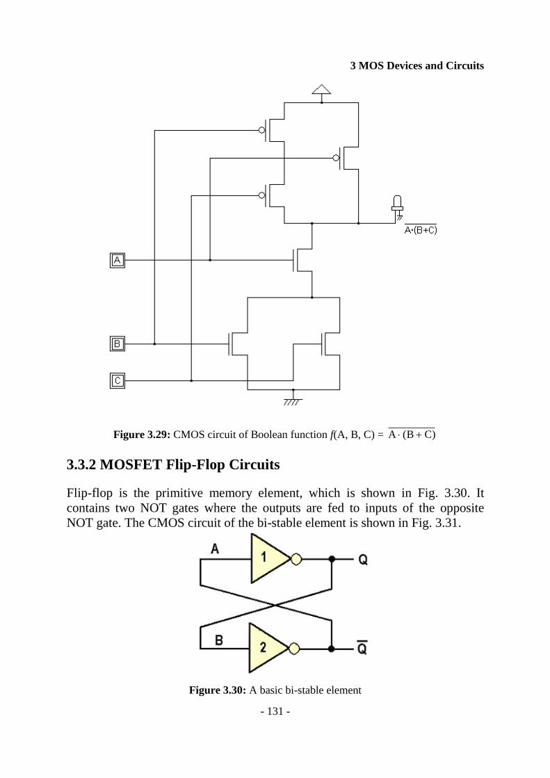
CMOS circuit of an two-input AND gate is shown in Fig. 3.28. The circuit
consist of a NAND gate connected to a NOT gate.
Figure 3.28: CMOS circuit of an AND gate
One of the most powerful aspects of building logic circuit in CMOS is the
ability to create a single circuit that provides several logic operations in the
integrated manner. This is called complex or combinational logic gates. Let‟s
consider the Boolean function f(A, B, C) = )CB(A . Based on this function,
one can see that the simplest way to design the function is one OR gate and one
NAND gate. This shall mean that to design this function, a total of ten MOS
transistors are required. Owing to the design constraint on a VLSI design, one
ought to consider the performance and the number of MOS transistor on the
silicon chip. Thus, the traditional approach should not be used as the straight
forward design. The AND-OR-NOT AOI and OR-AND-NOT OAI circuit
approaches shall be used, which required utilizing the Shannon‟s expansion of
the Boolean function to determine the OAI circuits.
Based on the logic function f(A, B, C) = )CB(A , the circuit of the logic
is shown in Fig. 3.29.
3 MOS Devices and Circuits
- 131 -
Figure 3.29: CMOS circuit of Boolean function f(A, B, C) = )CB(A
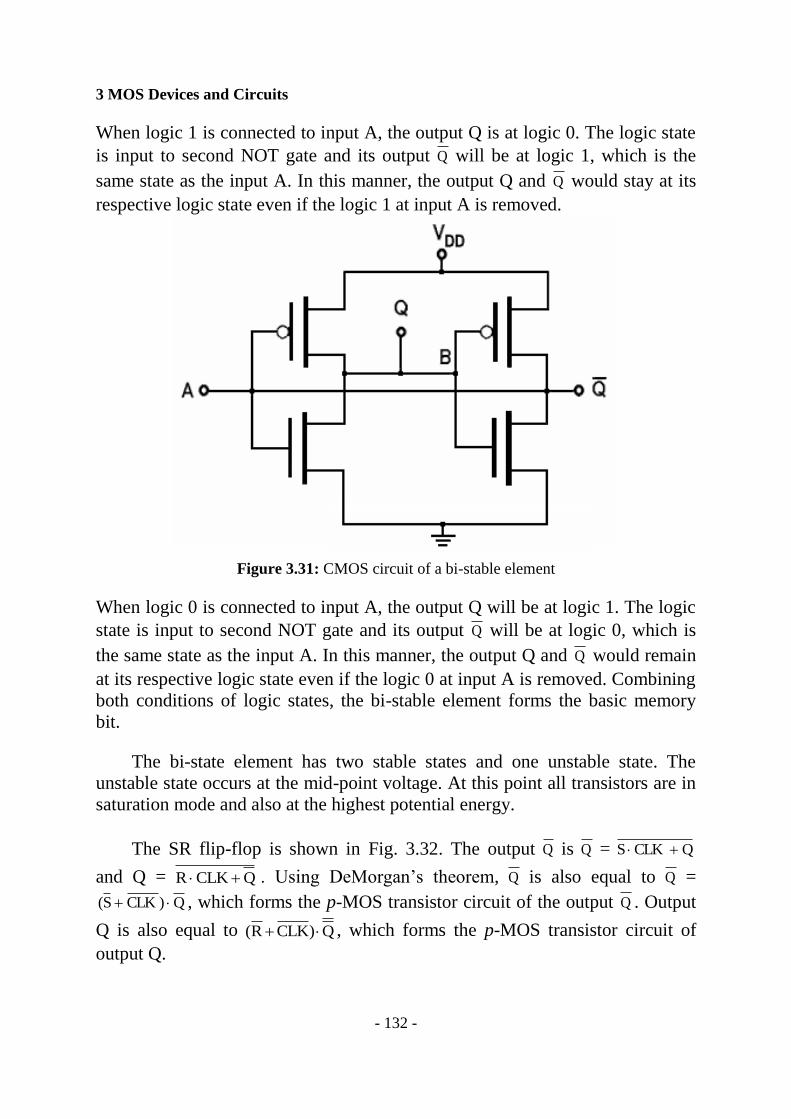
3.3.2 MOSFET Flip-Flop Circuits
Flip-flop is the primitive memory element, which is shown in Fig. 3.30. It
contains two NOT gates where the outputs are fed to inputs of the opposite
NOT gate. The CMOS circuit of the bi-stable element is shown in Fig. 3.31.
Figure 3.30: A basic bi-stable element
3 MOS Devices and Circuits
- 132 -
When logic 1 is connected to input A, the output Q is at logic 0. The logic state
is input to second NOT gate and its output Q will be at logic 1, which is the
same state as the input A. In this manner, the output Q and Q would stay at its
respective logic state even if the logic 1 at input A is removed.
Figure 3.31: CMOS circuit of a bi-stable element
When logic 0 is connected to input A, the output Q will be at logic 1. The logic
state is input to second NOT gate and its output Q will be at logic 0, which is
the same state as the input A. In this manner, the output Q and Q would remain
at its respective logic state even if the logic 0 at input A is removed. Combining
both conditions of logic states, the bi-stable element forms the basic memory
bit.
The bi-state element has two stable states and one unstable state. The
unstable state occurs at the mid-point voltage. At this point all transistors are in
saturation mode and also at the highest potential energy.
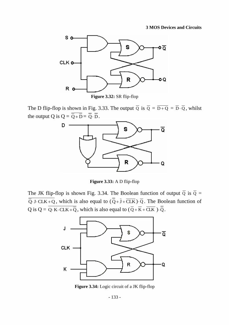
The SR flip-flop is shown in Fig. 3.32. The output Q is Q = QCLKS
and Q = QCLKR . Using DeMorgan‟s theorem, Q is also equal to Q =
Q)CLKS( , which forms the p-MOS transistor circuit of the output Q . Output
Q is also equal to Q)CLKR( , which forms the p-MOS transistor circuit of
output Q.
3 MOS Devices and Circuits
- 133 -
Figure 3.32: SR flip-flop
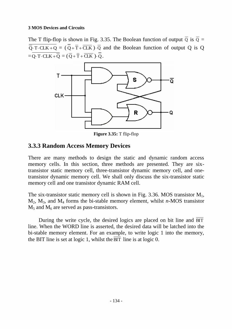
The D flip-flop is shown in Fig. 3.33. The output Q is Q = QD = QD , whilst
the output Q is Q = DQ = DQ .
Figure 3.33: A D flip-flop
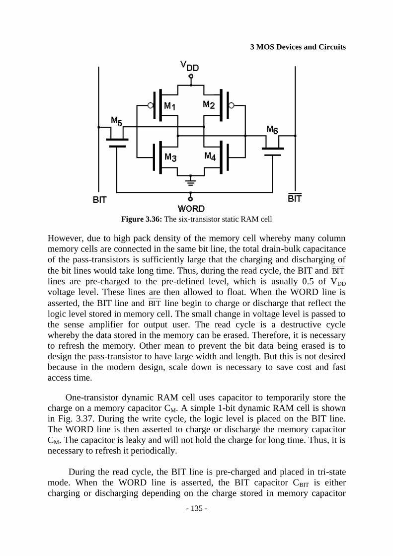
The JK flip-flop is shown Fig. 3.34. The Boolean function of output Q is Q =
QCLKJQ , which is also equal to ( CLKJQ ) Q . The Boolean function of
Q is Q = QCLKKQ , which is also equal to ( CLKKQ ) Q .
Figure 3.34: Logic circuit of a JK flip-flop
3 MOS Devices and Circuits
- 134 -
The T flip-flop is shown in Fig. 3.35. The Boolean function of output Q is Q =
QCLKTQ = ( CLKTQ ) Q and the Boolean function of output Q is Q
= QCLKTQ = ( CLKTQ ) Q .
Figure 3.35: T flip-flop
3.3.3 Random Access Memory Devices
There are many methods to design the static and dynamic random access
memory cells. In this section, three methods are presented. They are six-
transistor static memory cell, three-transistor dynamic memory cell, and one-
transistor dynamic memory cell. We shall only discuss the six-transistor static
memory cell and one transistor dynamic RAM cell.
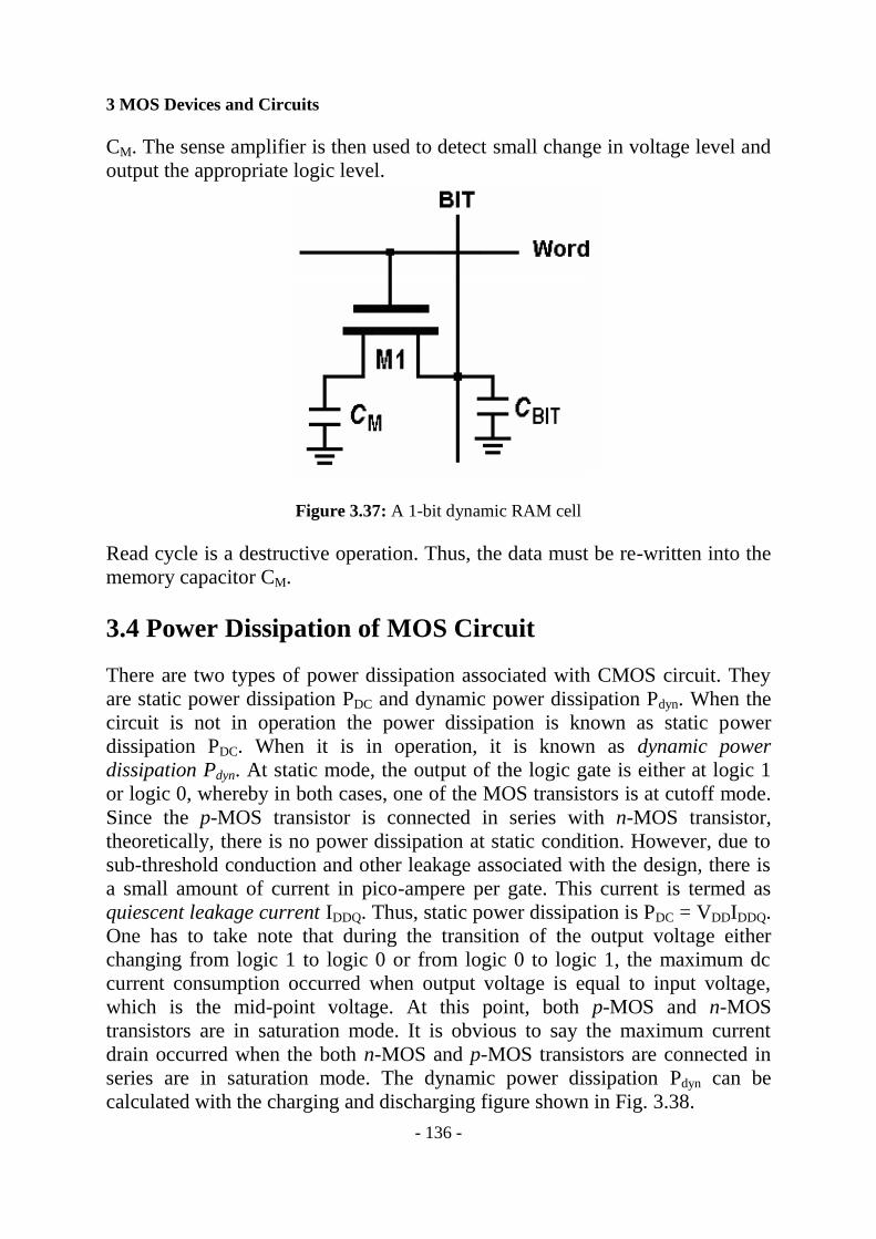
The six-transistor static memory cell is shown in Fig. 3.36. MOS transistor M1,
M2, M3, and M4 forms the bi-stable memory element, whilst n-MOS transistor
M5 and M6 are served as pass-transistors.
During the write cycle, the desired logics are placed on bit line and BIT
line. When the WORD line is asserted, the desired data will be latched into the
bi-stable memory element. For an example, to write logic 1 into the memory,
the BIT line is set at logic 1, whilst the BIT line is at logic 0.
3 MOS Devices and Circuits
- 135 -
Figure 3.36: The six-transistor static RAM cell
However, due to high pack density of the memory cell whereby many column
memory cells are connected in the same bit line, the total drain-bulk capacitance
of the pass-transistors is sufficiently large that the charging and discharging of
the bit lines would take long time. Thus, during the read cycle, the BIT and BIT
lines are pre-charged to the pre-defined level, which is usually 0.5 of VDD
voltage level. These lines are then allowed to float. When the WORD line is
asserted, the BIT line and BIT line begin to charge or discharge that reflect the
logic level stored in memory cell. The small change in voltage level is passed to
the sense amplifier for output user. The read cycle is a destructive cycle
whereby the data stored in the memory can be erased. Therefore, it is necessary
to refresh the memory. Other mean to prevent the bit data being erased is to
design the pass-transistor to have large width and length. But this is not desired
because in the modern design, scale down is necessary to save cost and fast
access time.
One-transistor dynamic RAM cell uses capacitor to temporarily store the
charge on a memory capacitor CM. A simple 1-bit dynamic RAM cell is shown
in Fig. 3.37. During the write cycle, the logic level is placed on the BIT line.
The WORD line is then asserted to charge or discharge the memory capacitor
CM. The capacitor is leaky and will not hold the charge for long time. Thus, it is
necessary to refresh it periodically.
During the read cycle, the BIT line is pre-charged and placed in tri-state
mode. When the WORD line is asserted, the BIT capacitor CBIT is either
charging or discharging depending on the charge stored in memory capacitor
3 MOS Devices and Circuits
- 136 -
CM. The sense amplifier is then used to detect small change in voltage level and
output the appropriate logic level.
Figure 3.37: A 1-bit dynamic RAM cell
Read cycle is a destructive operation. Thus, the data must be re-written into the
memory capacitor CM.
3.4 Power Dissipation of MOS Circuit
There are two types of power dissipation associated with CMOS circuit. They
are static power dissipation PDC and dynamic power dissipation Pdyn. When the
circuit is not in operation the power dissipation is known as static power
dissipation PDC. When it is in operation, it is known as dynamic power
dissipation Pdyn. At static mode, the output of the logic gate is either at logic 1
or logic 0, whereby in both cases, one of the MOS transistors is at cutoff mode.
Since the p-MOS transistor is connected in series with n-MOS transistor,
theoretically, there is no power dissipation at static condition. However, due to
sub-threshold conduction and other leakage associated with the design, there is
a small amount of current in pico-ampere per gate. This current is termed as
quiescent leakage current IDDQ. Thus, static power dissipation is PDC = VDDIDDQ.
One has to take note that during the transition of the output voltage either
changing from logic 1 to logic 0 or from logic 0 to logic 1, the maximum dc
current consumption occurred when output voltage is equal to input voltage,
which is the mid-point voltage. At this point, both p-MOS and n-MOS
transistors are in saturation mode. It is obvious to say the maximum current
drain occurred when the both n-MOS and p-MOS transistors are connected in
series are in saturation mode. The dynamic power dissipation Pdyn can be
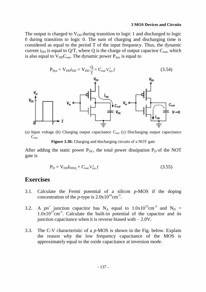
calculated with the charging and discharging figure shown in Fig. 3.38.
3 MOS Devices and Circuits
- 137 -
The output is charged to VDD during transition to logic 1 and discharged to logic
0 during transition to logic 0. The sum of charging and discharging time is
considered as equal to the period T of the input frequency. Thus, the dynamic
current iDD is equal to Q/T, where Q is the charge of output capacitor Cout, which
is also equal to VDDCout. The dynamic power Pdyn is equal to
Pdyn = VDDiDD = VDDT
Q= Cout f2
DDV (3.54)
(a) Input voltage (b) Charging output capacitance Cout (c) Discharging output capacitance
Cout Figure 3.38: Charging and discharging circuits of a NOT gate
After adding the static power PDC, the total power dissipation PD of the NOT
gate is
PD = VDDIDDQ + Cout f2
DDV (3.55)
Exercises
3.1. Calculate the Fermi potential of a silicon p-MOS if the doping
concentration of the p-type is 2.0x10¹⁶
cm-3
.
3.2. A pn+ junction capacitor has NA equal to 1.0x10
15cm
-3 and ND =
1.0x10¹⁷
cm-3
. Calculate the built-in potential of the capacitor and its
junction capacitance when it is reverse biased with – 2.0V.
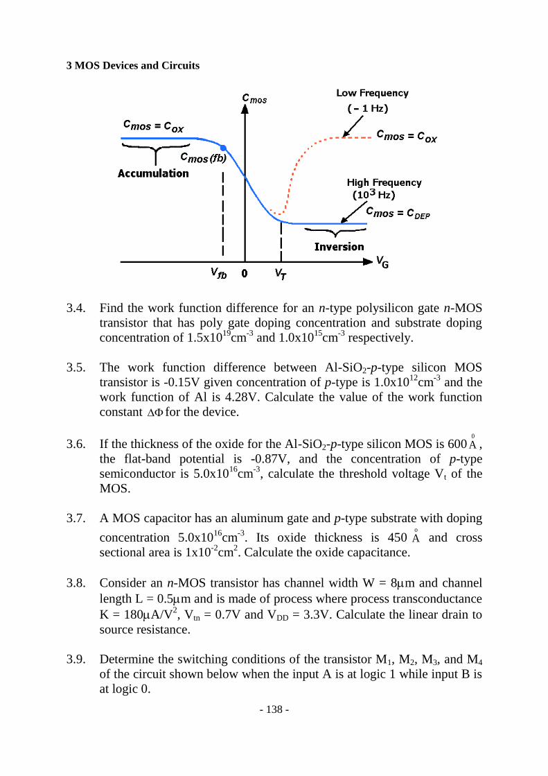
3.3. The C-V characteristic of a p-MOS is shown in the Fig. below. Explain
the reason why the low frequency capacitance of the MOS is
approximately equal to the oxide capacitance at inversion mode.
3 MOS Devices and Circuits
- 138 -
3.4. Find the work function difference for an n-type polysilicon gate n-MOS
transistor that has poly gate doping concentration and substrate doping
concentration of 1.5x10¹⁹
cm-3
and 1.0x10¹⁵
cm-3
respectively.
3.5. The work function difference between Al-SiO2-p-type silicon MOS
transistor is -0.15V given concentration of p-type is 1.0x10¹²
cm-3
and the
work function of Al is 4.28V. Calculate the value of the work function
constant for the device.
3.6. If the thickness of the oxide for the Al-SiO2-p-type silicon MOS is 600 A0
,
the flat-band potential is -0.87V, and the concentration of p-type
semiconductor is 5.0x10¹⁶
cm-3
, calculate the threshold voltage Vt of the
MOS.
3.7. A MOS capacitor has an aluminum gate and p-type substrate with doping
concentration 5.0x10¹⁶
cm-3
. Its oxide thickness is 450 Ao
and cross
sectional area is 1x10⁻²
cm2. Calculate the oxide capacitance.
3.8. Consider an n-MOS transistor has channel width W = 8m and channel
length L = 0.5m and is made of process where process transconductance
K = 180A/V2, Vtn = 0.7V and VDD = 3.3V. Calculate the linear drain to
source resistance.
3.9. Determine the switching conditions of the transistor M1, M2, M3, and M4
of the circuit shown below when the input A is at logic 1 while input B is
at logic 0.
3 MOS Devices and Circuits
- 139 -
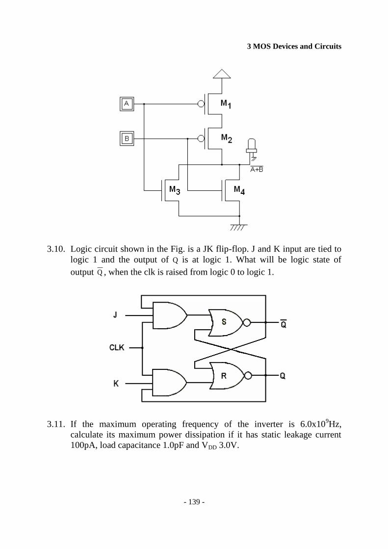
3.10. Logic circuit shown in the Fig. is a JK flip-flop. J and K input are tied to
logic 1 and the output of Q is at logic 1. What will be logic state of
output Q , when the clk is raised from logic 0 to logic 1.
3.11. If the maximum operating frequency of the inverter is 6.0x10⁹Hz,
calculate its maximum power dissipation if it has static leakage current
100pA, load capacitance 1.0pF and VDD 3.0V.
3 MOS Devices and Circuits
- 140 -
Bibliography
1. John P. Uyemura, “Chip Design for Submicron VLSI: CMOS Layout and
Simulation”, Thomson, 2006.
2. Etienne Sicard and Sonia Delmas Bendhia, “Basics of CMOS Cell
Design”, TATA McGraw Hill, 2006.
3. Jasprit Singh, “Semiconductor Device”, McGraw Hill Inc. 1994.
Index
- 97 -
0
0.8µm technology ................................. 122
A
Accumulation mode ................................ 99
AND-OR-NOT circuit .......................... 130
B
Bi-stable element .................................. 131
Bulk threshold parameter ...................... 111
C
Channel length ...................................... 121
Combinational logic gate ...................... 130
Constant Mobility Approximation Model
................................................... 115, 117
Constant-field scaling ........................... 123
Constant-voltage scaling ....................... 123
Cut-off frequency .................................. 121
D
DeMorgan‟s theorem ............................ 132
Depletion charge ................................... 110
Depletion mode ....................................... 99
Diffusion ............................................... 117
Drain conductance ................................ 120
Dynamic power dissipation................... 136
E
Electric field .......................................... 110
F
Flat-band voltage .................................. 111
Flip-flop ................................................ 131
G
Gradual Channel Approximation Model
................................................... 115, 116
I
intrinsic energy level ............................... 97
Inversion mode........................................ 99
J
JK flip-flop ............................................ 133
K
Kirchhoff‟s voltage law ................ 108, 112
L
Lightly doped drain............................... 123
Lithography........................................... 122
M
Memory
Dynamic RAM .................................. 135
Mobility ........................................ 116, 121
Mobility degradation parameter ........... 116
MOSFET ................................ 97, 112, 126
depletion-enhancement ...................... 112
enhancement ...................................... 112
N
NAND gate ........................................... 130
nMOS ...................................................... 97
NOR gate .............................................. 129
NOT gate .............................................. 129
npn transistor ........................................ 111
O
OAI circuit ............................................ 130
OR gate ................................................. 129
OR-AND-NOT circuit .......................... 130
P
pMOS ...................................................... 97
pnp transistor ........................................ 111
Poisson‟s equation ................................ 115
polysilicon .............................................. 97
Q
Quiescent leakage current ..................... 136
S
Scale factor ........................................... 123
silicon dioxide ......................................... 97
Silicon dioxide ...................................... 112
Si-SiO2 .................................................. 107
Six-transistor static memory cell .......... 134
SR flip-flop ........................................... 132
Static power dissipation ........................ 136
Surface charge density .......................... 109
Surface potential ................................... 101
T
T flip-flop.............................................. 134
Index
- 98 -
Taylor‟s series ....................................... 118
Threshold voltage.......... 108, 110, 120, 124
Transconductance ......................... 115, 120
Tri-state ................................................. 124
U
Ultra deep submicron technology ......... 122
W
Work function ....................................... 109
Z
Zero body bias ...................................... 111
Recommended