CMSC Lecture 03
• Moore’s “Law”
• Evolution of the Pentium Chip• IA-32 Basic Execution Environment
• IA-32 General Purpose Registers
• “Hello World” in Linux Assembly Language• Addressing Modes
UMBC, CMSC313, Richard Chang <[email protected]>

Moore’s “Law”
• In the mid-1960’s, Intel Chairman of the Board Gordon Moore observed that “the number of transistors that would be incorporated on a silicon die would double every 18 months for the next several years.”
• His prediction has continued to hold true.• Perhaps a self-fulfilling prophecy?
UMBC, CMSC313, Richard Chang <[email protected]>

2-7
INTRODUCTION TO THE IA-32 INTEL ARCHITECTURE
2.3. MOORE’S LAW AND IA-32 PROCESSOR GENERATIONS
In the mid-1960s, Intel Chairman of the Board Gordon Moore made an observation: “the
number of transistors that would be incorporated on a silicon die would double every 18 months
for the next several years”. Over the past three and half decades, this prediction has continued
to hold true that it is often referred to as “Moore's Law.”
The computing power and the complexity (or roughly, the number of transistors per processor)
of Intel architecture processors has grown, over the years, in close relation to Moore's law. By
taking advantage of new process technology and new micro-architecture designs, each new
generations of IA-32 processors have demonstrated frequency-scaling headroom and new
performance levels over the previous generation processors. The key features of the Intel
Pentium 4 processor and Pentium III processor with advanced transfer cache are shown in Table
2-1. Older generation of IA-32 processors, which do not employ on-die second-level cache, are
shown in Table 2-2.
Table 2-1. Key Features of contemporary IA-32 processors
NOTES:
1. The register size and external data bus size are given in bits.2. First level cache is denoted using the abbreviation L1, 2nd level cache is denoted as L2.
3. Intel Pentium III and Pentium III Xeon processors, with advanced transfer cache and built on 0.18 micronprocess technology, were introduced in October 1999.
Intel Processor
Date Intro-duced
Micro-architecture
Clock Frequency
at Intro-duction
Transis-tors per
Die
Register Sizes1
System Bus
Bandwidth
Max. Extern. Addr. Space
On-die Caches2
Pentium III processor3
1999 P6 700 MHz 28 M GP: 32 FPU: 80 MMX: 64
XMM: 128
Up to 1.06 GB/s
64 GB 32KB L1;256KB L2
Pentium 4 processor
2000 Intel NetBurst micro-
architecture
1.50 GHz 42 M GP: 32 FPU: 80 MMX: 64
XMM: 128
3.2 GB/s
64 GB 12K µop Execution
Trace Cache;8KB L1;
256KB L2

2-8
INTRODUCTION TO THE IA-32 INTEL ARCHITECTURE
NOTES:
1. The register size and external data bus size are given in bits. Note also that each 32-bit general-purpose
(GP) registers can be addressed as an 8- or a 16-bit data registers in all of the processors
2. Internal data paths that are 2 to 4 times wider than the external data bus for each processor.
2.4. THE P6 FAMILY MICRO-ARCHITECTURE
The Pentium Pro processor introduced a new micro-architecture for the Intel IA-32 processors,commonly referred to as P6 processor microarchitecture. The P6 processor micro-architecturewas later enhanced with an on-die, 2nd level cache, called Advanced Transfer Cache. Thismicro-architecture is a three-way superscalar, pipelined architecture. The term “three-waysuperscalar” means that using parallel processing techniques, the processor is able on averageto decode, dispatch, and complete execution of (retire) three instructions per clock cycle. Tohandle this level of instruction throughput, the P6 processor family use a decoupled, 12-stagesuperpipeline that supports out-of-order instruction execution. Figure 2-1 shows a conceptualview of the P6 processor micro-architecture pipeline with the Advanced Transfer Cacheenhancement. The micro-architecture pipeline is divided into four sections (the 1st level and 2ndlevel caches, the front end, the out-of-order execution core, and the retire section). Instructionsand data are supplied to these units through the bus interface unit.
Table 2-2. Key Features of previous generations of IA-32 Processor
Intel Processor Date Intro-duced
Max. Clock Frequency
at Intro-duction
Transis-tors
per Die
Register Sizes1
Ext. Data Bus Size2
Max. Extern. Addr. Space
Caches
8086 1978 8 MHz 29 K 16 GP 16 1 MB None
Intel 286 1982 12.5 MHz 134 K 16 GP 16 16 MB Note 3
Intel386 DX Processor 1985 20 MHz 275 K 32 GP 32 4 GB Note 3
Intel486 DX Processor 1989 25 MHz 1.2 M 32 GP
80 FPU
32 4 GB L1: 8KB
Pentium Processor 1993 60 MHz 3.1 M 32 GP
80 FPU
64 4 GB L1:16KB
Pentium Pro Processor 1995 200 MHz 5.5 M 32 GP
80 FPU
64 64 GB L1: 16KB
L2: 256KB
or 512KB
Pentium II Processor 1997 266 MHz 7 M 32 GP
80 FPU
64 MMX
64 64 GB L1: 32KB
L2: 256KB
or 512KB
Pentium III Processor 1999 500 MHz 8.2 M 32 GP
80 FPU
64 MMX
128
XMM
64 64 GB L1: 32KB
L2: 512KB

3-3
BASIC EXECUTION ENVIRONMENT
Figure 3-1. IA-32 Basic Execution Environment
0
232
-1
Eight 32-bit
32-bits
32-bits
General-Purpose Registers
Segment Registers
EFLAGS Register
EIP (Instruction Pointer Register)
Address Space*
*The address space can be
Six 16-bit
Registers
Registers
Eight 80-bit
Registers
Floating-Point
Data Registers
Eight 64-bit
RegistersMMX Registers
flat or segmented. Using
XMM RegistersEight 128-bit
Registers
16-bits Control Register
16-bits Status Register
48-bits FPU Instruction Pointer Register
48-bits FPU Data (Operand) Pointer Register
FPU Registers
MMX Registers
SSE and SSE2 Registers
32-bits MXCSR Register
Opcode Register (11-bits)
Basic Program Execution Registers
16-bits Tag Register
the physical address
extension mechanism, a
physical address space of
236
-1 can be addressed.

3-10
BASIC EXECUTION ENVIRONMENT
3.4.2. Segment Registers
The segment registers (CS, DS, SS, ES, FS, and GS) hold 16-bit segment selectors. A segment
selector is a special pointer that identifies a segment in memory. To access a particular segment
in memory, the segment selector for that segment must be present in the appropriate segment
register.
When writing application code, programmers generally create segment selectors with assembler
directives and symbols. The assembler and other tools then create the actual segment selector
values associated with these directives and symbols. If writing system code, programmers may
need to create segment selectors directly. (A detailed description of the segment-selector data
structure is given in Chapter 3, Protected-Mode Memory Management, of the Intel ArchitectureSoftware Developer’s Manual, Volume 3.)
How segment registers are used depends on the type of memory management model that the
operating system or executive is using. When using the flat (unsegmented) memory model, the
segment registers are loaded with segment selectors that point to overlapping segments, each of
which begins at address 0 of the linear address space (as shown in Figure 3-5). These overlap-
ping segments then comprise the linear address space for the program. (Typically, two overlap-
ping segments are defined: one for code and another for data and stacks. The CS segment
register points to the code segment and all the other segment registers point to the data and stack
segment.)
When using the segmented memory model, each segment register is ordinarily loaded with a
different segment selector so that each segment register points to a different segment within the
linear address space (as shown in Figure 3-6). At any time, a program can thus access up to six
segments in the linear address space. To access a segment not pointed to by one of the segment
registers, a program must first load the segment selector for the segment to be accessed into a
segment register.
Figure 3-4. Alternate General-Purpose Register Names
071531 16 8
AH AL
BH BL
CH CL
DH DL
BP
SI
DI
SP
16-bit
AX
DX
CX
BX
32-bit
EAX
EBX
ECX
EDX
EBP
ESI
ESP
General-Purpose Registers
EDI

3-9
BASIC EXECUTION ENVIRONMENT
• EIP (instruction pointer) register. The EIP register contains a 32-bit pointer to the nextinstruction to be executed.
3.4.1. General-Purpose Registers
The 32-bit general-purpose registers EAX, EBX, ECX, EDX, ESI, EDI, EBP, and ESP areprovided for holding the following items:
• Operands for logical and arithmetic operations
• Operands for address calculations
• Memory pointers.
Although all of these registers are available for general storage of operands, results, andpointers, caution should be used when referencing the ESP register. The ESP register holds thestack pointer and as a general rule should not be used for any other purpose.
Many instructions assign specific registers to hold operands. For example, string instructionsuse the contents of the ECX, ESI, and EDI registers as operands. When using a segmentedmemory model, some instructions assume that pointers in certain registers are relative tospecific segments. For instance, some instructions assume that a pointer in the EBX registerpoints to a memory location in the DS segment.
The special uses of general-purpose registers by instructions are described in Chapter 5, Instruc-tion Set Summary, in this volume and Chapter 3, Instruction Set Reference, in the Intel Architec-ture Software Developer’s Manual, Volume 2. The following is a summary of these special uses:
• EAX—Accumulator for operands and results data.
• EBX—Pointer to data in the DS segment.
• ECX—Counter for string and loop operations.
• EDX—I/O pointer.
• ESI—Pointer to data in the segment pointed to by the DS register; source pointer for stringoperations.9
• EDI—Pointer to data (or destination) in the segment pointed to by the ES register;destination pointer for string operations.
• ESP—Stack pointer (in the SS segment).
• EBP—Pointer to data on the stack (in the SS segment).
As shown in Figure 3-4, the lower 16 bits of the general-purpose registers map directly to theregister set found in the 8086 and Intel 286 processors and can be referenced with the namesAX, BX, CX, DX, BP, SP, SI, and DI. Each of the lower two bytes of the EAX, EBX, ECX, andEDX registers can be referenced by the names AH, BH, CH, and DH (high bytes) and AL, BL,CL, and DL (low bytes).

“Hello World” in Linux Assembly
• Use your favorite UNIX editor (vi, emacs, pico, ...)
• Assemble using NASM on gl.umbc.edunasm -f elf hello.asm
• NASM documentation is on-line.
• Need to “load” the object fileld hello.o
• Executea.out
• CMSC 121 Introduction to UNIXUMBC, CMSC313, Richard Chang <[email protected]>

80x86 Addressing Modes
• We want to store the value 1734h.
• The value 1734h may be located in a register
or in memory.
• The location in memory might be specified
by the code, by a register, …
• Assembly language syntax for MOV
MOV DEST, SOURCE

EAXEBXECXEDXEBPESIEDIESP
EIP
Register from Register
MOV EAX, ECX
Data
Code
.
.
.
MOV…
1734
Addressing Modes

EAXEBXECXEDXEBPESIEDIESP
EIP
Register from Register Indirect
MOV EAX, [ECX]
Data
Code
.
.
.
MOV…
08A94068
1734
Addressing Modes

EAXEBXECXEDXEBPESIEDIESP
EIP
Register from Memory
MOV EAX, [08A94068]
MOV EAX, [x]
Data
Code
.
.
.
08A94068
MOV…
1734
Addressing Modes
x

EAXEBXECXEDXEBPESIEDIESP
EIP
Register from Immediate
MOV EAX, 1734
Data
Code
.
.
.
1734
MOV…
Addressing Modes
EAXEBXECXEDXEBPESIEDIESP
EIP
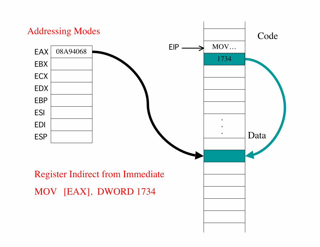
Register Indirect from Immediate
MOV [EAX], DWORD 1734
Data
Code
.
.
.
1734
MOV…08A94068
Addressing Modes
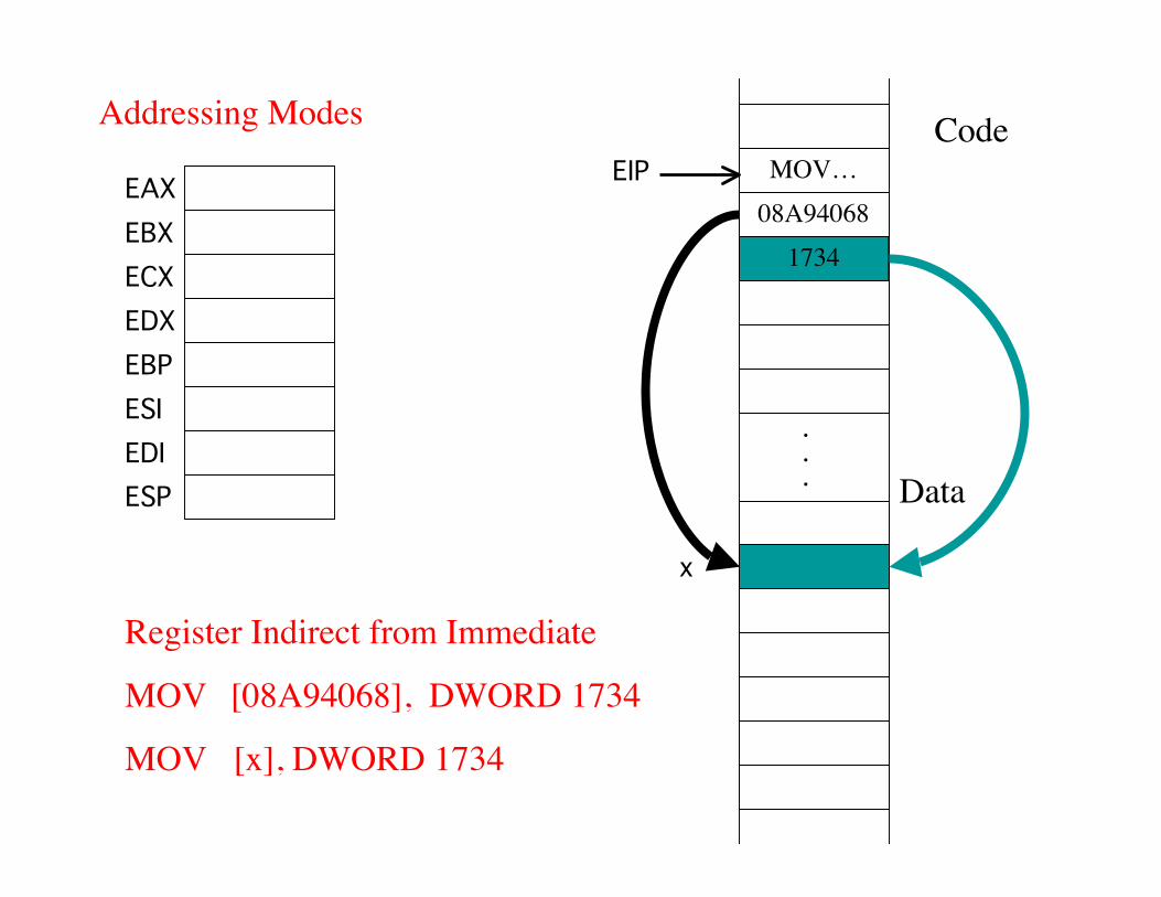
EAXEBXECXEDXEBPESIEDIESP
EIP
Register Indirect from Immediate
MOV [08A94068], DWORD 1734
MOV [x], DWORD 1734
Data
Code
.
.
.
1734
MOV…
08A94068
Addressing Modes
x

Notes on Addressing Modes
• More complicated addressing modes later:
MOV EAX, [ESI+4*ECX+12]
• Figures not drawn to scale. Constants 1734h
and 08A94068h take 4 bytes (little endian).
• Some addressing modes are not supported
by some operations.
• Labels represent addresses not contents of
memory.

toupper.asm
• Prompt for user input.
• Use Linux system call to get user input.
• Scan each character of user input and convert all lower case characters to upper case.
• How to:work with 8-bit data
specify ASCII constant
compare values
loop control
UMBC, CMSC313, Richard Chang <[email protected]>

Debugging Assembly Language Programs
• Cannot just put print statements everywhere.
• Use gdb to:examine contents of registers
exmaine contents of memory
set breakpoints
single-step through program
• READ THE GDB SUMMARY ONLINE!
UMBC, CMSC313, Richard Chang <[email protected]>

gdb ommand Summary
Command Example Description
run start program
quit quit out of gdb
cont continue execution after a break
break [addr] break *_start+5 sets a breakpoint
delete [n] delete 4 removes nth breakpoint
delete removes all breakpoints
info break lists all breakpoints
stepi execute next instruction
stepi [n] stepi 4 execute next n instructions
nexti execute next instruction, stepping over function calls
nexti [n] nexti 4 execute next n instructions, stepping over function calls
where show where execution halted
disas [addr] disas _start disassemble instructions at given address
info registers dump contents of all registers
print/d [expr] print/d $ecx print expression in decimal
print/x [expr] print/x $ecx print expression in hex
print/t [expr] print/t $ecx print expression in binary
x/NFU [addr] x/12xw &msg Examine contents of memory in given format
display [expr] display $eax automatically print the expression each time the program is halted
display/i $eip print machine instruction each time the program is halted
info display show list of automatically displays
undisplay [n] undisplay 1 remove an automatic display

Next Time
• Overview of i386 instruction set.
• Arithmetic instructions, logical instructions.
• EFLAGS register
UMBC, CMSC313, Richard Chang <[email protected]>
Recommended