Embed Size (px)
Citation preview
CMSC 313 Lecture 25
• Registers
• Memory Organization• DRAM
UMBC, CMSC313, Richard Chang <[email protected]>

Appendix A: Digital LogicA-75
Principles of Computer Architecture by M. Murdocca and V. Heuring © 1999 M. Murdocca and V. Heuring
Four-Bit Register• Makes use of tri-state buffers so that multiple registers can gang
their outputs to common output lines.
D3
Q3
D2
Q2
D1
Q1
D0
Q0
WR
EN
QD
D3
Write (WR)
Enable (EN)
Q3
QD
D2
Q2
QD
D1
Q1
QD
D0
Q0
CLK

Appendix A: Digital LogicA-76
Principles of Computer Architecture by M. Murdocca and V. Heuring © 1999 M. Murdocca and V. Heuring
Left-RightShift
Registerwith
ParallelRead and
Write
D3
Q3
D2
Q2
D1
Q1
D0
Q0
Shift right inputShift right output
Shift right inputShift left output
c0c1
Control Functionc0c1
0011
0101
No changeShift leftShift rightParallel load
QD
D3
Enable (EN)
Q3
QD
D2
Q2
QD
D1
Q1
QD
D0
Q0
CLK
c0
c1
Shift right input
c0
c1
Shift right output
Shift right input
Shift left output
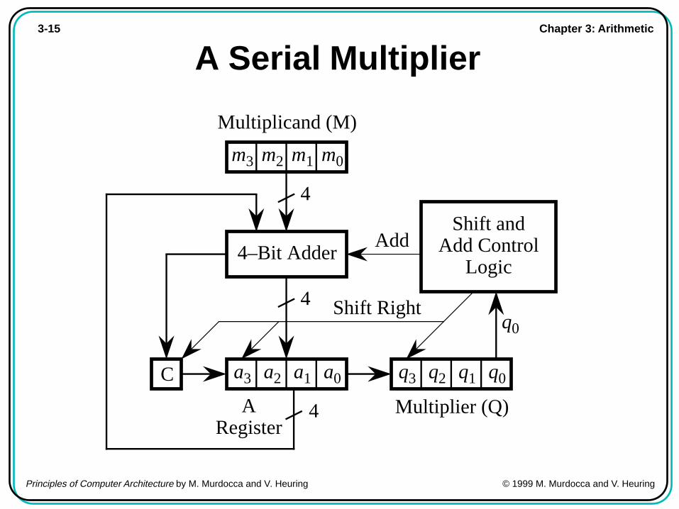
Chapter 3: Arithmetic3-15
Principles of Computer Architecture by M. Murdocca and V. Heuring © 1999 M. Murdocca and V. Heuring
A Serial Multiplier
Multiplicand (M)
m0m1m2m3
a0a1a2a3 q0q1q2q3
Multiplier (Q)
C
4–Bit Adder
Shift and Add Control
LogicAdd
4
4
4
Shift Rightq0
A Register

Chapter 3: Arithmetic3-16
Principles of Computer Architecture by M. Murdocca and V. Heuring © 1999 M. Murdocca and V. Heuring
Example of Multiplication UsingSerial Multiplier
C
0
00
10
0
10
0
A
0 0 0
1 1 0 10 1 1 0
0 0 1 11 0 0 1
0 1 0 0
0 0 0 11 0 0 0
1
Q
0 1 1
1 0 1 11 1 0 1
1 1 0 11 1 1 0
1 1 1 1
1 1 1 11 1 1 1
Multiplicand (M):
1 1 0 1Initial values
Add M to AShift
Add M to AShift
Shift (no add)
Add M to AShift
Product

Chapter 7: Memory7-4
Principles of Computer Architecture by M. Murdocca and V. Heuring © 1999 M. Murdocca and V. Heuring
Functional Behavior of a RAM Cell
QD
CLK
Read
Select
Data In/Out

Chapter 7: Memory7-5
Principles of Computer Architecture by M. Murdocca and V. Heuring © 1999 M. Murdocca and V. Heuring
Simplified RAM Chip Pinout
A0-Am-1 D0-Dw-1
WR
CS
Memory Chip

Chapter 7: Memory7-6
Principles of Computer Architecture by M. Murdocca and V. Heuring © 1999 M. Murdocca and V. Heuring
A Four-WordMemory withFour Bits perWord in a 2DOrganization
D3D2
D1D0
Q3Q2
Q1Q0
WR
CSWord 0
00
01
10
11
A0
A1
WR
WR
CSWord 1
WR
CSWord 2
WR
CSWord 3
2-to-4decoder
Chip Select(CS)

Chapter 7: Memory7-7
Principles of Computer Architecture by M. Murdocca and V. Heuring © 1999 M. Murdocca and V. Heuring
A Simplified Representation of theFour-Word by Four-Bit RAM
Q3 Q2 Q1 Q0
A0
A1
WR
CS
D3 D2 D1 D0
4× 4 RAM

Chapter 7: Memory7-8
Principles of Computer Architecture by M. Murdocca and V. Heuring © 1999 M. Murdocca and V. Heuring
2-1/2D Organization of a 64-Word byOne-Bit RAM
RowDec-oder
Column Decoder (MUX/DEMUX)
A0
A1
A2
A3A4
A5
Data
One Stored Bit
QD
CLK
Read
Row Select
Column Select
Data In/Out
Read/WriteControl
Two bits wide:One bit for data andone bit for select.

Appendix A: Digital LogicA-33
Principles of Computer Architecture by M. Murdocca and V. Heuring © 1999 M. Murdocca and V. Heuring
Decoder
D0
A D1
D2
D3
B
0001
1011
0011
0101
A B
1000
D0
0100
D1
0010
D2
0001
D3
D3 = A BD1 = A B D2 = A BD0 = A B
Enable
Enable = 1
0011
0101
A B
0000
D0
0000
D1
0000
D2
0000
D3
Enable = 0

Chapter 7: Memory7-9
Principles of Computer Architecture by M. Murdocca and V. Heuring © 1999 M. Murdocca and V. Heuring
Two Four-Word by Four-Bit RAMs areUsed in Creating a Four-Word by
Eight-Bit RAM
A0
A1
WRCS
D7 D6 D5 D4 D3 D2 D1 D0
4× 4 RAM
Q7 Q6 Q5 Q4 Q3 Q2 Q1 Q0
4× 4 RAM

Chapter 7: Memory7-10
Principles of Computer Architecture by M. Murdocca and V. Heuring © 1999 M. Murdocca and V. Heuring
Two Four-Word by Four-Bit RAMs Makeup an Eight-Word by Four-Bit RAM
A0
A1
WR
D3 D2 D1 D0
4× 4 RAM
Q3 Q2 Q1 Q0
4× 4 RAM
1-to-2decoder
0
1A2
CS
CS
CS

Chapter 7: Memory7-11
Principles of Computer Architecture by M. Murdocca and V. Heuring © 1999 M. Murdocca and V. Heuring
Single-In-Line Memory Module
1
2
3
4
5
6
7
8
9
10
11
12
13
14
15
16
17
18
19
20
21
22
23
24
25
26
27
28
29
30
Vcc
CAS
DQ1
A0
A1
DQ2
A2
A3
Vss
DQ3
A4
A5
DQ4
A6
A7
DQ5
A8
A9
NC
DQ6
W
Vss
DQ7
NC
DQ8
NC
RAS
NC
NC
Vcc
PIN NOMENCLATURE
Address InputsColumn-Address Strobe
Data In/Data OutNo Connection
Row-Address Strobe5-V Supply
GroundWrite Enable
DQ1-DQ8
CASA0-A9
NC
RASVccVssW
• Adaptedfrom(Texas Instru-ments, MOSMemory: Commer-cial and MilitarySpecifications DataBook , Texas Instru-ments, LiteratureResponse Center,P.O. Box 172228,Denver, Colorado,1991.)
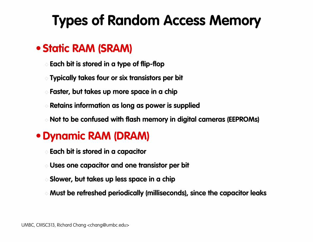
Types of Random Access Memory
• Static RAM (SRAM)Each bit is stored in a type of flip-flop
Typically takes four or six transistors per bit
Faster, but takes up more space in a chip
Retains information as long as power is supplied
Not to be confused with flash memory in digital cameras (EEPROMs)
• Dynamic RAM (DRAM)Each bit is stored in a capacitor
Uses one capacitor and one transistor per bit
Slower, but takes up less space in a chip
Must be refreshed periodically (milliseconds), since the capacitor leaks
UMBC, CMSC313, Richard Chang <[email protected]>

DRAM
• A DRAM memory cell
GND
Word Line
Bit Line
Capacitor
• Word line selects cell for reading or writing
• To write, the bit line is charged with logic 1 or 0
• To read, sensitive amplifier circuits detect small changes in bit line.
• Reading discharges the capacitor.
UMBC, CMSC313, Richard Chang <[email protected]>


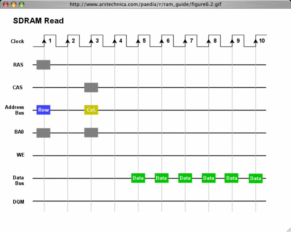
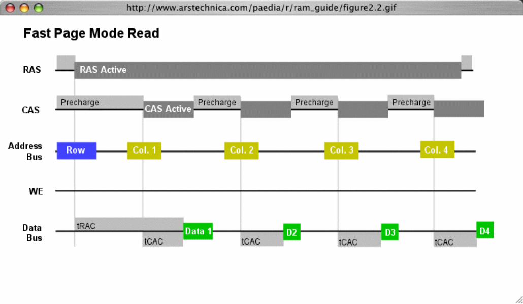
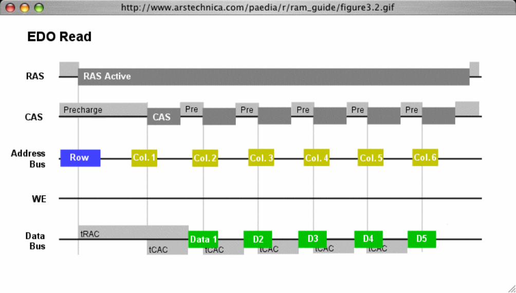
DRAM Read Cycle
1. Row address placed on the address bus.
2. Row Address Strobe (RAS) is asserted, allowing the row address to latch.
3. Row address decoder selects proper row.
4. Write Enable (WE) disabled.
5. Column address placed on the address bus.
6. Column Address Strobe (CAS) is activated, allowing the column address to latch.
7. Once the CAS signal has stabilized, sensing amplifiers places data from the selected row & column on data bus.
8. RAS and CAS deactivated. Cycle begins again.
UMBC, CMSC313, Richard Chang <[email protected]>


DRAM
• DRAM is asynchronous, ignores system bus clock.tRAC = Row Access Time = delay from RAS assertion until data is ready
tCAC = Column Access Time = delay from CAS assertion until data is ready
• DRAM access is sloooooow
• Each memory access must wait for time it takes to activate and deactivate RAS.
• Fast Page Mode (FPM) DRAM allows successive reads from the same row without deactivating RAS.
• Extended Data Out (EDO) DRAM overlaps CAS assertion and data reads.
UMBC, CMSC313, Richard Chang <[email protected]>

Synchronous DRAM (SDRAM)
• Uses system bus clock.
• Current models run at 433MHz (still much slower than CPU).
• Burst mode allows fast successive reads from the same row. (Good way to read in a cache line!)
• Double Data Rate (DDR) SDRAM provides data on the positive and negative edges of the clock.
UMBC, CMSC313, Richard Chang <[email protected]>