1
Schematic Layout
Microwave Office Training
2 Schematic Layout
Schematic Layout
Schematic
View
Schematic Layout
View
Circuit
Artwork Cells
Two views of the same circuit!
- including connectivity (ratslines)
External World
•GDSII
•DXF
Need Cell
Faces or
Cell Pins
External World
Need
Export
MappingWe are Here!
2
3 Schematic Layout
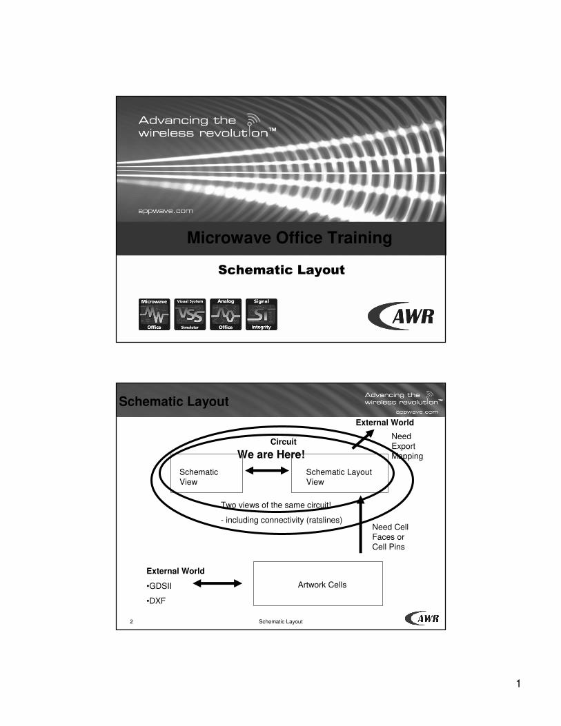
Summary - Schematic and Layout
• The Circuit has two different views
– Schematic View: The traditional Schematic
– Layout View: The traditional Layout
• The two views are related
– Connectivity of Elements
– Physical Parameters of PCells - length, width,...
• PCells have two properties menus
– Element Properties control the parameters, symbol,...
– Shape Properties control what layers, how snaps together...
• Connectivity
– Schematic View: Nodes connected by wires
– Layout View: Elements connected at faces
4 Schematic Layout
Schematic and Layout Views
Schematic View Schematic Layout View
Electrical Model of Element Layout and Connectivity
Note: Not all elements have layout Parameterized Cells
(PCells)
Can also draw shapes -
ground fills, etc.
Remember - These are Drawing Layers!
3
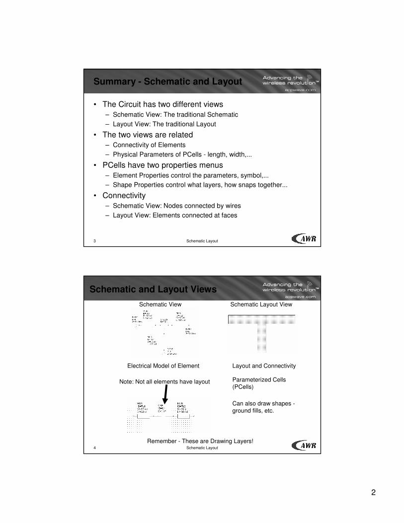
5 Schematic Layout
Example Board Stackup
•FR4 - Er = 3.38, tand = .003 @ 1 GHz
•Conductors - Copper, Thickness = 1.4 mil
•Dielectric Layers - 25 mil thick
Microstrip
Ground and
Coplanar Lines
Stripline
Ground AWR_Bottom_Ground
AWR_Mid_Copper
AWR_Mid_Ground
AWR_Top_Copper
AWR_PCB3
AWR_PCB2
AWR_PCB1
AWR_Via34
AWR_Via23
AWR_Via12
Metal LayersDielectric LayersVia Layers
Tip: Use easy to identify names! (These all have AWR_ in
front of them.) Helps when layers are added.
This is configured as a Library: AWR_4Layer_PCB
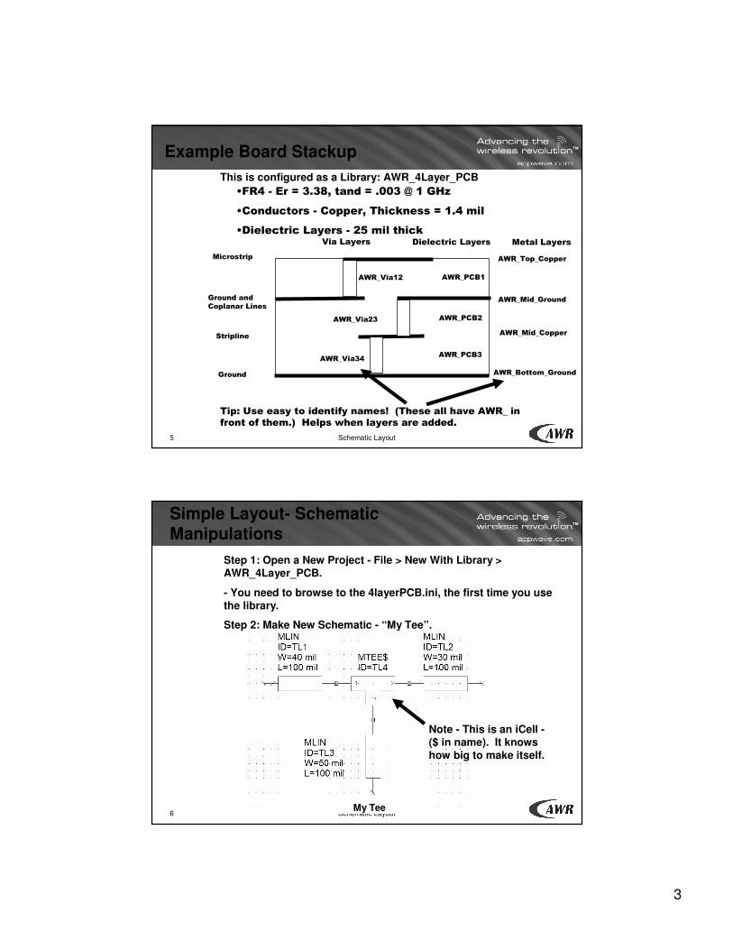
6 Schematic Layout
Simple Layout- Schematic Manipulations
Step 1: Open a New Project - File > New With Library > AWR_4Layer_PCB.
- You need to browse to the 4layerPCB.ini, the first time you usethe library.
Step 2: Make New Schematic - “My Tee”.
Note - This is an iCell -($ in name). It knows how big to make itself.
My Tee
4
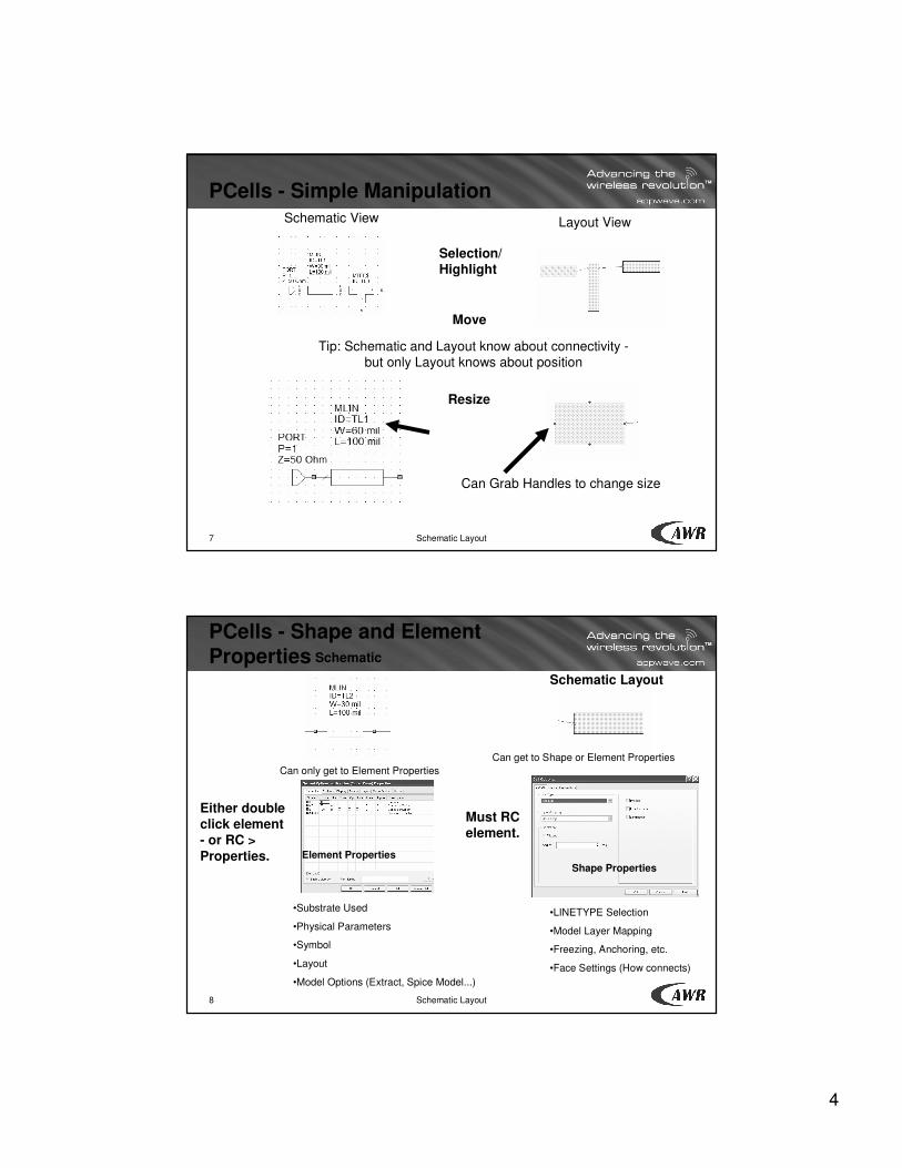
7 Schematic Layout
PCells - Simple ManipulationSchematic View Layout View
Move
Tip: Schematic and Layout know about connectivity -
but only Layout knows about position
Resize
Selection/Highlight
Can Grab Handles to change size
8 Schematic Layout
PCells - Shape and Element Properties Schematic
Schematic Layout
Can only get to Element Properties
Can get to Shape or Element Properties
•Substrate Used
•Physical Parameters
•Symbol
•Layout
•Model Options (Extract, Spice Model...)
•LINETYPE Selection
•Model Layer Mapping
•Freezing, Anchoring, etc.
•Face Settings (How connects)
Element Properties
Shape Properties
Either double click element - or RC > Properties.
Must RC element.
5
9 Schematic Layout
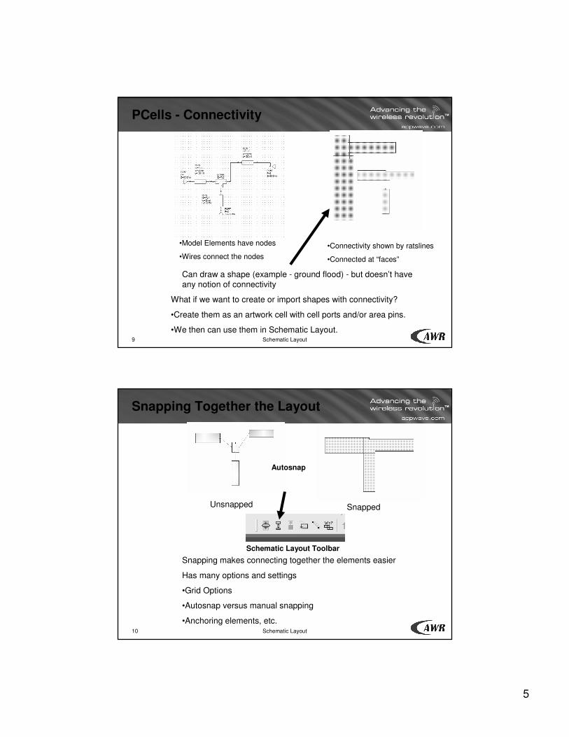
PCells - Connectivity
•Model Elements have nodes
•Wires connect the nodes
•Connectivity shown by ratslines
•Connected at “faces”
What if we want to create or import shapes with connectivity?
•Create them as an artwork cell with cell ports and/or area pins.
•We then can use them in Schematic Layout.
Can draw a shape (example - ground flood) - but doesn’t have
any notion of connectivity
10 Schematic Layout
Snapping Together the Layout
Unsnapped Snapped
Snapping makes connecting together the elements easier
Has many options and settings
•Grid Options
•Autosnap versus manual snapping
•Anchoring elements, etc.
Autosnap
Schematic Layout Toolbar
6
11 Schematic Layout
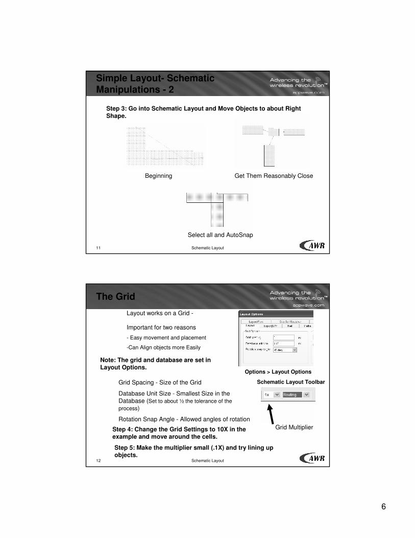
Simple Layout- Schematic Manipulations - 2
Step 3: Go into Schematic Layout and Move Objects to about RightShape.
Beginning Get Them Reasonably Close
Select all and AutoSnap
12 Schematic Layout
The Grid
Layout works on a Grid -
Important for two reasons
- Easy movement and placement
-Can Align objects more Easily
Grid Spacing - Size of the Grid
Database Unit Size - Smallest Size in the
Database (Set to about ½ the tolerance of the
process)
Rotation Snap Angle - Allowed angles of rotation
Grid Multiplier
Options > Layout Options
Step 4: Change the Grid Settings to 10X in the example and move around the cells.
Step 5: Make the multiplier small (.1X) and try lining up objects.
Schematic Layout Toolbar
Note: The grid and database are set in Layout Options.
7
13 Schematic Layout
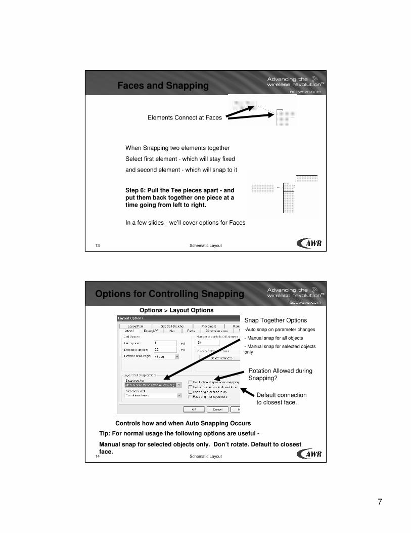
Faces and Snapping
Elements Connect at Faces
When Snapping two elements together
Select first element - which will stay fixed
and second element - which will snap to it
Step 6: Pull the Tee pieces apart - and put them back together one piece at a time going from left to right.
In a few slides - we’ll cover options for Faces
14 Schematic Layout
Options for Controlling Snapping
Controls how and when Auto Snapping Occurs
Options > Layout Options
Snap Together Options
-Auto snap on parameter changes
- Manual snap for all objects
- Manual snap for selected objects
only
Rotation Allowed during
Snapping?
Default connection
to closest face.
Tip: For normal usage the following options are useful -
Manual snap for selected objects only. Don’t rotate. Default to closest face.
8
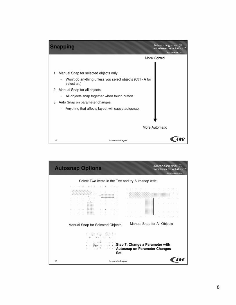
15 Schematic Layout
Snapping
1. Manual Snap for selected objects only
- Won’t do anything unless you select objects (Ctrl - A for
select all.)
2. Manual Snap for all objects.
- All objects snap together when touch button.
3. Auto Snap on parameter changes
- Anything that affects layout will cause autosnap.
More Control
More Automatic
16 Schematic Layout
Autosnap Options
Select Two items in the Tee and try Autosnap with:
Manual Snap for Selected Objects Manual Snap for All Objects
Step 7: Change a Parameter with Autosnap on Parameter Changes Set.
9
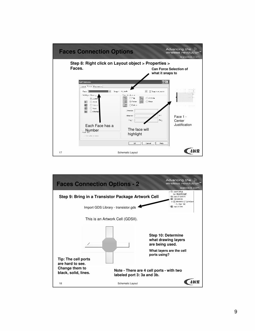
17 Schematic Layout
Faces Connection Options
Step 8: Right click on Layout object > Properties > Faces.
Face 1 -
Center JustificationEach Face has a
Number The face will
highlight
Can Force Selection of what it snaps to
18 Schematic Layout
Faces Connection Options - 2
Step 9: Bring in a Transistor Package Artwork Cell
Import GDS Library - transistor.gds
This is an Artwork Cell (GDSII).
Step 10: Determine what drawing layers are being used.
What layers are the cell ports using?
Note - There are 4 cell ports - with two labeled port 3: 3a and 3b.
Tip: The cell ports are hard to see. Change them to black, solid, lines.
10
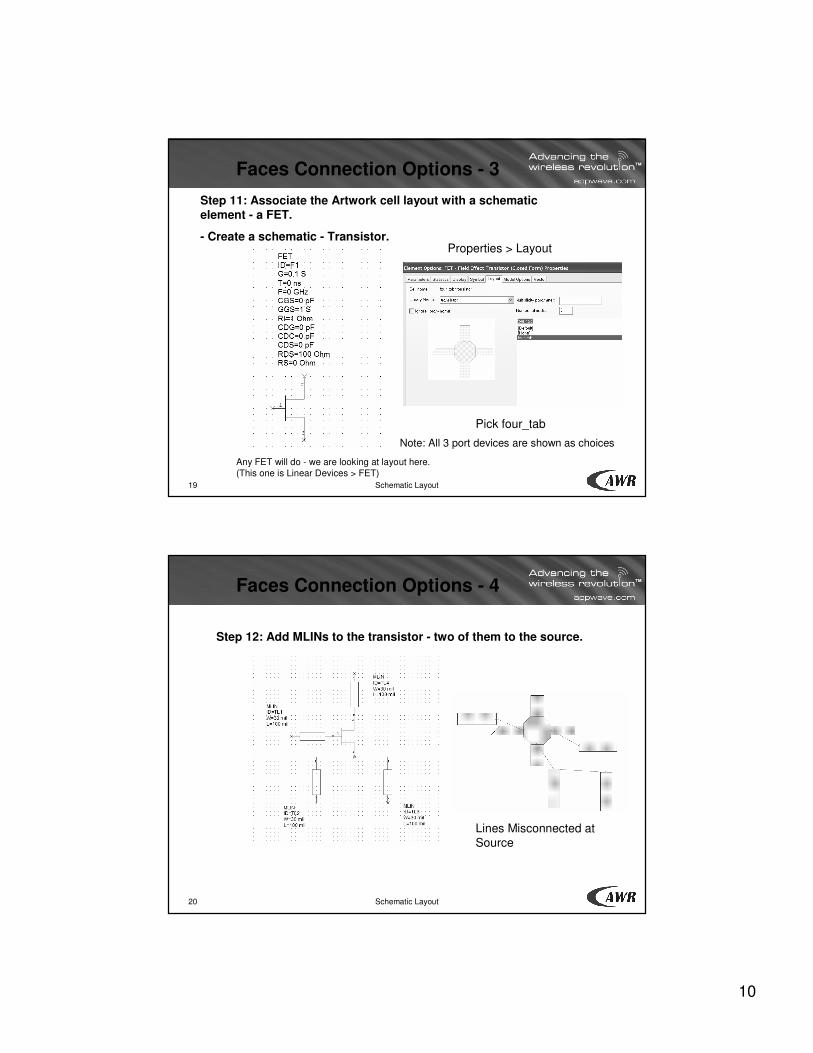
19 Schematic Layout
Faces Connection Options - 3
Step 11: Associate the Artwork cell layout with a schematic element - a FET.
- Create a schematic - Transistor.
Any FET will do - we are looking at layout here.
(This one is Linear Devices > FET)
Properties > Layout
Pick four_tab
Note: All 3 port devices are shown as choices
20 Schematic Layout
Faces Connection Options - 4
Step 12: Add MLINs to the transistor - two of them to the source.
Lines Misconnected at
Source
11
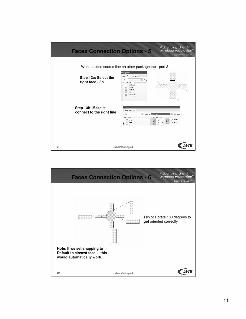
21 Schematic Layout
Faces Connection Options - 5
Want second source line on other package tab - port 3
Step 13a: Select the right face - 3b.
Step 13b: Make it connect to the right line
22 Schematic Layout
Faces Connection Options - 6
Flip or Rotate 180 degrees to
get oriented correctly
Note: If we set snapping to Default to closest face ... this would automatically work.
12
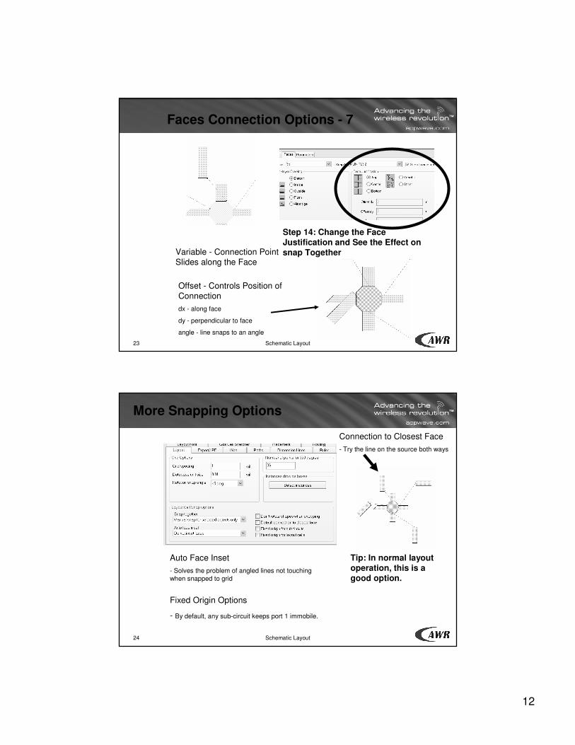
23 Schematic Layout
Faces Connection Options - 7
Step 14: Change the Face Justification and See the Effect on snap Together
Offset - Controls Position of
Connection
dx - along face
dy - perpendicular to face
angle - line snaps to an angle
Variable - Connection Point
Slides along the Face
24 Schematic Layout
More Snapping Options
Connection to Closest Face
- Try the line on the source both ways
Auto Face Inset
- Solves the problem of angled lines not touching
when snapped to grid
Fixed Origin Options
- By default, any sub-circuit keeps port 1 immobile.
Tip: In normal layout operation, this is a good option.
13
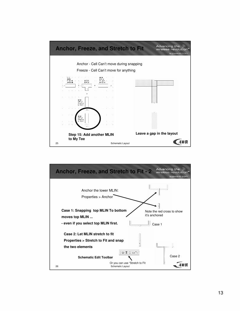
25 Schematic Layout
Anchor, Freeze, and Stretch to Fit
Anchor - Cell Can’t move during snapping
Freeze - Cell Can’t move for anything
Step 15: Add another MLIN to My Tee
Leave a gap in the layout
26 Schematic Layout
Anchor, Freeze, and Stretch to Fit - 2
Anchor the lower MLIN:
Properties > Anchor
Note the red cross to show
it’s anchored
Case 2: Let MLIN stretch to fit
Properties > Stretch to Fit and snap
the two elements
Case 1: Snapping top MLIN To bottom
moves top MLIN ...
- even if you select top MLIN first.
Or you can use “Stretch to Fit
Case 1
Case 2Schematic Edit Toolbar
14
27 Schematic Layout
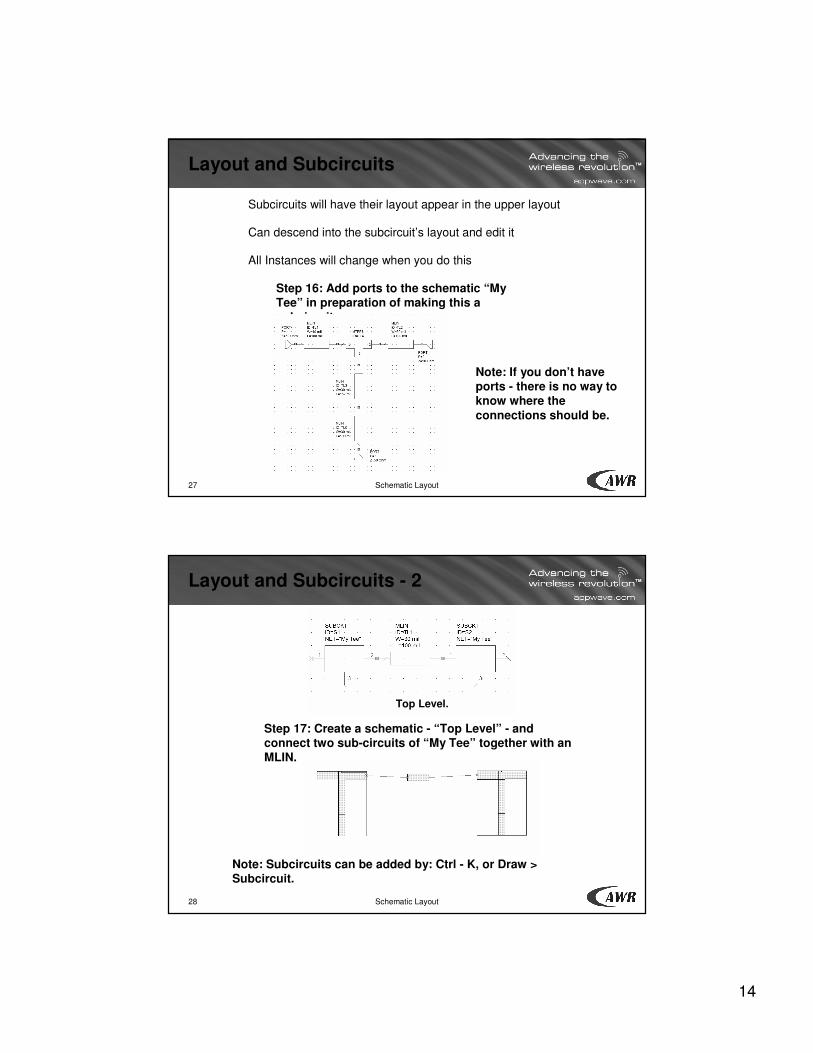
Layout and Subcircuits
Subcircuits will have their layout appear in the upper layout
Can descend into the subcircuit’s layout and edit it
All Instances will change when you do this
Step 16: Add ports to the schematic “My Tee” in preparation of making this a subcircuit
Note: If you don’t have ports - there is no way to know where the connections should be.
28 Schematic Layout
Layout and Subcircuits - 2
Step 17: Create a schematic - “Top Level” - and connect two sub-circuits of “My Tee” together with an MLIN.
Top Level.
Note: Subcircuits can be added by: Ctrl - K, or Draw > Subcircuit.
15
29 Schematic Layout
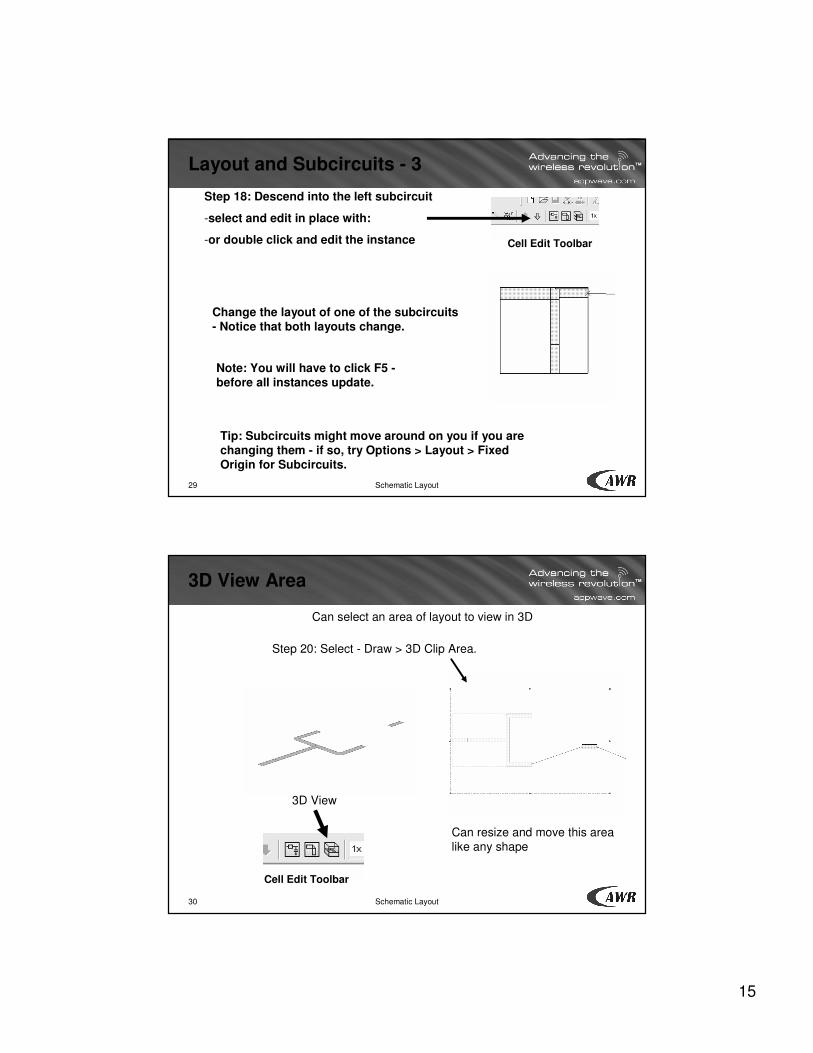
Layout and Subcircuits - 3
Step 18: Descend into the left subcircuit
-select and edit in place with:
-or double click and edit the instance
Change the layout of one of the subcircuits- Notice that both layouts change.
Note: You will have to click F5 -before all instances update.
Cell Edit Toolbar
Tip: Subcircuits might move around on you if you are changing them - if so, try Options > Layout > Fixed Origin for Subcircuits.
30 Schematic Layout
3D View Area
Can select an area of layout to view in 3D
Step 20: Select - Draw > 3D Clip Area.
3D View
Can resize and move this area
like any shape
Cell Edit Toolbar
Recommended